US4710803A - Color filter and color image sensor using the same - Google Patents
Color filter and color image sensor using the same Download PDFInfo
- Publication number
- US4710803A US4710803A US07/011,421 US1142187A US4710803A US 4710803 A US4710803 A US 4710803A US 1142187 A US1142187 A US 1142187A US 4710803 A US4710803 A US 4710803A
- Authority
- US
- United States
- Prior art keywords
- color
- photoelectric conversion
- image sensor
- signal
- pixel group
- Prior art date
- Legal status (The legal status is an assumption and is not a legal conclusion. Google has not performed a legal analysis and makes no representation as to the accuracy of the status listed.)
- Expired - Lifetime
Links
- 238000006243 chemical reaction Methods 0.000 claims abstract description 31
- 239000003086 colorant Substances 0.000 claims abstract description 20
- 239000011159 matrix material Substances 0.000 claims abstract description 9
- 238000003860 storage Methods 0.000 description 9
- 238000000034 method Methods 0.000 description 5
- 238000012937 correction Methods 0.000 description 3
- 238000012545 processing Methods 0.000 description 3
- 238000000151 deposition Methods 0.000 description 2
- 238000001259 photo etching Methods 0.000 description 2
- 230000035945 sensitivity Effects 0.000 description 2
- 239000000126 substance Substances 0.000 description 2
- XAGFODPZIPBFFR-UHFFFAOYSA-N aluminium Chemical compound [Al] XAGFODPZIPBFFR-UHFFFAOYSA-N 0.000 description 1
- 229910052782 aluminium Inorganic materials 0.000 description 1
- 239000003990 capacitor Substances 0.000 description 1
- 238000010276 construction Methods 0.000 description 1
- 230000008021 deposition Effects 0.000 description 1
- 238000010586 diagram Methods 0.000 description 1
- 238000001914 filtration Methods 0.000 description 1
- 238000003780 insertion Methods 0.000 description 1
- 230000037431 insertion Effects 0.000 description 1
- 238000004519 manufacturing process Methods 0.000 description 1
- 238000005259 measurement Methods 0.000 description 1
- 238000012986 modification Methods 0.000 description 1
- 230000004048 modification Effects 0.000 description 1
- 230000003287 optical effect Effects 0.000 description 1
- 230000001105 regulatory effect Effects 0.000 description 1
Images


Classifications
-
- H—ELECTRICITY
- H01—ELECTRIC ELEMENTS
- H01L—SEMICONDUCTOR DEVICES NOT COVERED BY CLASS H10
- H01L27/00—Devices consisting of a plurality of semiconductor or other solid-state components formed in or on a common substrate
- H01L27/14—Devices consisting of a plurality of semiconductor or other solid-state components formed in or on a common substrate including semiconductor components sensitive to infrared radiation, light, electromagnetic radiation of shorter wavelength or corpuscular radiation and specially adapted either for the conversion of the energy of such radiation into electrical energy or for the control of electrical energy by such radiation
- H01L27/144—Devices controlled by radiation
- H01L27/146—Imager structures
- H01L27/14643—Photodiode arrays; MOS imagers
- H01L27/14645—Colour imagers
-
- H—ELECTRICITY
- H04—ELECTRIC COMMUNICATION TECHNIQUE
- H04N—PICTORIAL COMMUNICATION, e.g. TELEVISION
- H04N25/00—Circuitry of solid-state image sensors [SSIS]; Control thereof
- H04N25/10—Circuitry of solid-state image sensors [SSIS]; Control thereof for transforming different wavelengths into image signals
- H04N25/11—Arrangement of colour filter arrays [CFA]; Filter mosaics
- H04N25/13—Arrangement of colour filter arrays [CFA]; Filter mosaics characterised by the spectral characteristics of the filter elements
- H04N25/134—Arrangement of colour filter arrays [CFA]; Filter mosaics characterised by the spectral characteristics of the filter elements based on three different wavelength filter elements
-
- H—ELECTRICITY
- H04—ELECTRIC COMMUNICATION TECHNIQUE
- H04N—PICTORIAL COMMUNICATION, e.g. TELEVISION
- H04N9/00—Details of colour television systems
- H04N9/11—Scanning of colour motion picture films, e.g. for telecine
Definitions
- the present invention relates to a color filter and a color image sensor using the same.
- a recently developed color printer reproduces a well-balanced color print by classifying a color original (such as a color negative film) into a plurality of scenes and regulating the degree of insertion of a color correction filter into an optical path of each scene.
- a color image sensor has been used to measure three color densities of the color original at each point of measurement thereon.
- a three-image type scanner or a single-image type sensor is used.
- three colors are separately measured by disposing three color filters, e.g. blue, green and red, at the light-receiving surface of each image sensor.
- a color filter with a mosaic pattern of blue color area, green color area and red color area is disposed at the receiving surface of the image sensor, which is cost effective.
- a color filter according to the present invention has (N-1) colors disposed in each row and in each column in an L shape, wherein N is an integer more than 3.
- (N-1) signal lines for each row and column are required so that the amount of wiring is reduced and hence the area for photoelectric conversion cells can be made large.
- red, green and blue colors are used for N colors and each color area is of L shape (including inverted L shape) disposed in a regular pattern.
- a color image sensor uses a color filter having (N-1) colors in the shape of an L disposed in each row and in each column, and a pixel group is made up of X ⁇ Y photoelectric conversion cells, wherein N, X and Y are each an integer more than 3.
- the combination of colors of the color filter may be red, green and blue, but specific colors such as flesh color may be added thereto.
- Another example of a color combination may be cyan, magenta and yellow.
- each color area has a uniform L shape so that the manufacture thereof is simple and there is little fear of peeling-off of the filter from the sensor.
- the photoelectric conversion cells of the same color can be uniformly distributed in the sensor.
- a single pixel group is made up of X ⁇ Y pixels, and signal charges of the same color are added within the pixel group and picked up so that it is possible to eliminate color registration. Furthermore, since pixels of the same color are positioned side by side, the wiring for adding signal charges is simplified.
- FIG. 1 is a perspective view of a color image sensor with its color filter removed, according to the present invention
- FIG. 2 is an enlarged plan view of a part of the color filter
- FIG. 3 illustrates the arrangement of a color image sensor according to the present invention, wherein a single pixel group is made up of X ⁇ Y pixels;
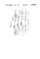
- FIG. 4 is a circuit diagram showing an example of an MOS-type color image sensor according to the present invention, wherein signal charges of the same color within a pixel group are added and picked up;
- FIG. 5 is a timing chart showing the timing of charge storage and signal readout.
- FIG. 1 shows a color image sensor. Disposed on a light-receiving surface of an IC chip 2 is a plurality of photoelectric conversion cells 4 in a matrix format. A color filter 6 having a plurality of different color areas of L shape is attached on the light-receiving surface 3. Instead of attaching the filter 6, a filtering substance may be directly deposited on the light-receiving surface 3 using a known photo-etching technique.
- FIG. 2 is an enlarged diagrammatic view of the color filter, wherein R denotes an area for selectively passing red color, G denotes an area for selectively passing green color, and B denotes an area for selectively passing blue color.
- R denotes an area for selectively passing red color
- G denotes an area for selectively passing green color
- B denotes an area for selectively passing blue color.
- These color areas may be formed by depositing colored substances on a transparent filter base using a known photo-etching technique.
- the color filter lacks one color for each row and column. For instance, red is missing from the first row and blue from the second row.
- the color area may be of continuous L shape, overlying three photoelectric conversion cells, or it may be made up of separate pieces positioned one over each of the three photoelectric conversion cells.
- FIG. 3 shows the arrangement of a color image sensor wherein signal charges of the same color within one pixel group are added together and picked up.
- the color image sensor 10 is constructed of, in a matrix arrangement, blue pixels 11 for photoelectrically converting blue light into a signal charge and storing it, green pixels 12 for photoelectrically converting green light into a signal charge and storing it, and red pixels 13 for photoelectrically converting red light into a signal charge and storing it. These pixels are constructed, as described previously, of photoelectric cells and color areas arranged thereupon.
- pixels of the same color are disposed in an L shape.
- the pixels are divided into pixel groups 10a.
- a pixel is surrounded by dotted lines
- pixel group is surrounded by solid lines.
- FIG. 4 shows an example of a MOS color image sensor using the pixel arrangement shown in FIG. 3.
- Photoelectric conversion cells are each shown by an equivalent photodiode.
- photodiodes 21 to 47 are exemplarily shown. These photodiodes convert incident light into signal charges and store them in floating capacitors.
- Photodiodes 21, 22, 24, 25, 33, 36, 39, 40 are 45 are used for blue color
- photodiodes 23, 26, 27, 29, 30, 32, 41, 42 and 44 are for green color
- photodiodes 28, 31, 34, 35 37, 38, 43, 46 and 47 are for red color.
- the photodiodes 21 to 23, 27 to 29 and 33 to 35 constitute a pixel group in the first row and the first column.
- three vertical MOS switches 51 to 53 are provided.
- Blue color photodiodes 21, 22 and 33 are connected to the blue color vertical MOS switch 51.
- When the blue color vertical MOS switch 51 turns ON three signal charges are picked up at the same time from a blue color vertical line 61 connected to the drain thereby to add signal charges within the pixel group.
- Green color photodiodes 23, 27 and 29 are connected to the source of the green color vertical MOS switch 52.
- the green color vertical MOS switch turns ON, three signal charges are picked up at the same time from a green color vertical line 62 to add signal charges.
- red color MOS switch 53 turns ON, three signal charges are added and picked up from a red color vertical line 63.
- a pixel group in the first row and the second column is constructed of photodiodes 24 to 26, 30 to 32, and 36 to 38.
- three vertical MOS switches 54 to 56 are provided.
- Vertical lines 64 to 66 are respectively connected to the drains of the vertical MOS switches 54 to 56.
- a pixel group at the second row and the first column is constructed of photodiodes 39 to 41, 42 to 44, and 45 to 47.
- three vertical MOS switches 57 to 59 are provided.
- Vertical lines 61 to 63 are connected to the vertical MOS switches 57 to 59.
- one vertical line and one horizontal line are provided for each row and column.
- a blue color horizontal line 71 is disposed on the first row
- a green color horizontal line 72 is disposed on the second row
- a red color horizontal line 73 is disposed on the third row.
- a blue color horizontal line 74 is disposed on the fourth row
- a green color horizontal line 75 is disposed on the fifth row
- a red color horizontal line 76 is disposed on the sixth row.
- These signal lines are formed by means of aluminum deposition. Since only a single signal line suffices for each row and each column, the wiring is simplified, and further the light-receiving surface of a photodiode is enlarged to a degree corresponding to the reduction in the amount of wiring.
- Vertical scan means 80 is constructed of a blue color vertical scan shift register 81, a green color vertical scan shift register 82, and a red color vertical scan shift register 83.
- the blue color horizontal line 71 is connected to the first output terminal D1 of the blue color vertical scan shift register 81, and the blue color horizontal line 74 is connected to the second output terminal D2.
- the green color horizontal line 72 is connected to the first output terminal D1 of the green color vertical scan shift register 82, and the green color horizontal lie 75 is connected to the second output terminal D2.
- the red color horizontal line 73 is connected to the first output terminal D1 of the red color vertical scan shift register 83, and the red color horizontal line 76 is connected to the second output terminal D2.
- the vertical lines 61 to 66 are respectively connected to the sources of horizontal MOS switches 85 to 90.
- the horizontal MOS switches 85 to 87 are used for picking up three color signals from the pixel groups in the first column, the gates of which are connected to the first output terminal F1 of a horizontal scan shift register 91.
- the horizontal MOS switches 88 to 90 are used for picking up three color signals from the pixel groups in the second column, the gates of which are connected to the second output terminal F2 of the horizontal scan shift register 91.
- a blue color output line 93 is connected to the drains of the blue color horizontal MOS switches 85 and 88, and a red color output line 94 is connected to the drains of the red color horizontal MOS switches 86 and 89.
- a green color output line 95 is connected to the green color horizontal MOS switches 87 and 90.
- Connected to the blue color output line 93 are: a MOS switch 97 for picking up effective signals, and a MOS switch 98 for draining signals read while periodically driving the color image sensor 10.
- two MOS switches 99 and 100 are connected to a red output line 94, and two MOS switched 101 and 102 are connected to a green ouput line 95.
- the drains of the MOS switches 97, 99 and 101 are picking up effective signals are connected to a single ouput line 103, while the drains of the MOS switches 98, 100 and 102 for draining unnecessary signals are connected to a single reset line 104.
- the operation of the vertical scan means 80 and the horizontal scan shift register 91 is controlled by a controller 106 to scan each pixel group and pick up each signal.
- the color image sensor 10 is actuated at a predetermined period, and it is necessary to drain unnecessary signals and pick up only effective signals.
- the controller 106 outputs EB, ER and EG signals for use in draining unnecessary signals to turn ON the MOS switches 98, 100 and 102, and outputs TSB, TSR and TSG signals for use in picking up effective signals to turn ON the MOS switches 97, 99 and 101.
- the controller 106 is further inputted with a start signal for a main scan and with a signal for setting charge storage time for each color.
- Reference numeral 107 denotes a pulse generator.
- Superposition of color signals is not permitted in the embodiment of FIG. 4. However, superposition may be performed by independently providing a horizontal scan shift register for each color and independently providing an output line 103 for each color.
- the charge storage time for each color is determined so as to have the maximum output value of the photoelectric conversion means near its saturation value. This value is set in the controller 106.
- the controller 106 drives the color image sensor 10 at a predetermined period in an ordinary scan to sequentially pick up three color signals. The readout signals during the ordinary scan are not needed, so they are drained from the reset line 104.
- the controller 106 actuates the vertical scan means 80 and the horizontal scan shift register 91 and outputs an EB, EG or ER signal for a color signal being read, thereby to turn ON the MOS switch 98, 100 or 102 to drain a read-out signal to the reset line 104.
- the controller 106 When a color original is placed in the reading position, the controller 106 is supplied with a readout start signal. Upon reception of this readout start signal, a main scan starts in synchronism with a vertical synchro signal for a color signal to be first read. In this embodiment, a blue color signal is first read, so the main scan starts at time t1.
- the controller 106 At time t1 when the main scan starts, the controller 106 outputs an EB signal to turn ON the MOS switch 98. Simultaneously therewith, the controller 106 supplies a shift pulse 108 to the blue color vertical shift register 81 and a shift pulse 109 to the horizontal scan shift register 81. The controller 106 supplies a clock pulse to the horizontal scan shift register 91 to perform a horizontal scan once. Every time a horizontal scan is completed, a clock pulse 110 is supplied to the vertical scan means 80 to perform vertical scan.
- the horizontal scan shift register 91 is shifted by a clock pulse 111 so that the second output terminal F2 becomes "H" to read a blue color signal from the pixel group in the first row and in the second column.
- the vertical and horizontal MOS horizontal switches 54 and 88 turn ON thereby to add signal charges stored in the blue color photodiodes 24, 25 and 36 and to pick them up from the blue color output line 93, which are in turn drained via the MOS switch 98 to the reset line 104.
- the controller supplies a clock pulse 110 to the vertical scan means 80, so that only the second output terminal D2 of the blue color vertical scan shift register 81 becomes "H".
- the horizontal scan shift register 91 is scanned once similarly to the above case, to add signal charges stored in the blue color pixels within the same pixel group in the second row and to pick them up and to drain them to the reset line 104.
- blue color signals in the third and following columns are sequentially read by scanning corresponding pixels. Reading blue color signals is carried out during time t1 to t2.
- the blue color pixels 11 of the image sensor 10 are sequentially reset in the unit of a pixel group to immediately thereafter start the charge storage for blue color pixels 11.
- green color pixels 12 After resetting the blue color pixels 11 at time t2, green color pixels 12 start to be reset.
- the controller 106 supplies a shift pulse 112 to the green color vertical scan shift register 82 and a shift pulse 109 to the horizontal scan shift register 91 to add green color signals and read them from each pixel group in a similar manner as previously described. Reading green color signals is carried out during time t2 to t3 wherein green color pixels 12 for each pixel group are sequentially reset to start charge storage.
- the MOS switch 100 After resetting green color pixels 12, the MOS switch 100 is turned ON to reset red color pixels 13 during time t3 to t4.
- Blue color charge storage terminates at time t5.
- Signal charges stored in the blue color pixels 11 are added and sequentially read in the unit of a pixel group using the blue color vertical scan shift register 81 and the horizontal scan shift register 91.
- the controller 106 outputs a TSB signal to turn ON the MOS signal 97 so that blue color time sequential signals added for each pixel group are picked up from the output line 103 and sent to a signal processing circuit (not shown).
- the signal processing circuit performs, as is well known, digital conversion, logarithmic conversion, color correction and the like to send obtained density signals to a microcomputer (not shown). Reading of the blue color signal is carried out during time t5 to t6.
- the signal charges stored in the green color pixels 12 are added and sequentially read in the unit of a pixel group, using the green color vertical scan shift register 82 and the horizontal scan shift register 91.
- the read-out charges are sent to the output line 103 via the MOS switch 101 in an ON state. Reading the green color signal is carried out during time t7 to t8.
- a main scan is performed during time t1 to t10 during which effective blue, green and red color signals are sequentially read.
- the controller 106 drives the image sensor for a predetermined period and drains the read-out signal to the reset line 104.
- resetting during the mains can is performed independently for each color.
- a reset signal is outputted from the controller and supplied at the same time to the gates of the MOS switches 98, 100 and 102, it is possible to reset the respective color pixels at the same time.
- a single signal line is provided for each row and for each column.
- two signal lines may be provided independently for two color photodiodes in each row and in each column, such that vertical MOS switches provided independently for each photodiode are each connected to two signal lines (horizontal and vertical signal lines).
- blue and green color horizontal lines are provided for the first row
- red and green color horizontal lines are provided for the second row
- red and blue color horizontal lines are provided for the third row.
- Two horizontal lines for the same color are connected together to couple them to the first output terminal D1 of each of the vertical scan shift registers 81 to 83.
- two vertical liens are provided for each column, and two vertical lines of the same color within the same pixel group are connected together to couple them to each of the horizontal MOS switches provided for the respective colors.
- the color filter according to this invention is applicable not only when the signal charges stored in the photoelectric conversion cells are added within the same pixel group for each color and picked up, but also when signal charges are not added but a signal charge in each photoelectric conversion cell is separately picked up. Furthermore, the invention is also applicable to image sensors of a CCD type.
Landscapes
- Physics & Mathematics (AREA)
- Engineering & Computer Science (AREA)
- Power Engineering (AREA)
- Signal Processing (AREA)
- Multimedia (AREA)
- Electromagnetism (AREA)
- Condensed Matter Physics & Semiconductors (AREA)
- General Physics & Mathematics (AREA)
- Spectroscopy & Molecular Physics (AREA)
- Computer Hardware Design (AREA)
- Microelectronics & Electronic Packaging (AREA)
- Color Television Image Signal Generators (AREA)
- Solid State Image Pick-Up Elements (AREA)
- Facsimile Heads (AREA)
- Facsimile Scanning Arrangements (AREA)
- Color Image Communication Systems (AREA)
Applications Claiming Priority (2)
| Application Number | Priority Date | Filing Date | Title |
|---|---|---|---|
| JP61-22155 | 1986-02-05 | ||
| JP61022155A JPH0638662B2 (ja) | 1986-02-05 | 1986-02-05 | カラ−イメ−ジセンサ− |
Publications (1)
| Publication Number | Publication Date |
|---|---|
| US4710803A true US4710803A (en) | 1987-12-01 |
Family
ID=12074949
Family Applications (1)
| Application Number | Title | Priority Date | Filing Date |
|---|---|---|---|
| US07/011,421 Expired - Lifetime US4710803A (en) | 1986-02-05 | 1987-02-03 | Color filter and color image sensor using the same |
Country Status (4)
| Country | Link |
|---|---|
| US (1) | US4710803A (de) |
| EP (1) | EP0233065B1 (de) |
| JP (1) | JPH0638662B2 (de) |
| DE (1) | DE3785773T2 (de) |
Cited By (17)
| Publication number | Priority date | Publication date | Assignee | Title |
|---|---|---|---|---|
| US4768084A (en) * | 1985-09-28 | 1988-08-30 | Hitachi, Ltd. | Solid-state imaging device with two-row mixing gates |
| US4989075A (en) * | 1987-08-26 | 1991-01-29 | Kabushiki Kaisha Toshiba | Solid-state image sensor device |
| US5031032A (en) * | 1990-03-30 | 1991-07-09 | Xerox Corporation | Color array for use in fabricating full width arrays |
| US5043817A (en) * | 1988-12-23 | 1991-08-27 | Hitachi, Ltd. | Image pick-up apparatus with electronic zooming-in |
| US5087809A (en) * | 1990-11-26 | 1992-02-11 | Eastman Kodak Company | Spectrally selective dithering and color filter mask for increased image sensor blue sensitivity |
| US5105264A (en) * | 1990-09-28 | 1992-04-14 | Eastman Kodak Company | Color image sensor having an optimum exposure time for each color |
| US5119181A (en) * | 1990-03-30 | 1992-06-02 | Xerox Corporation | Color array for use in fabricating full width arrays |
| US5841554A (en) * | 1994-01-31 | 1998-11-24 | Canon Kabushiki Kaisha | Image pickup apparatus |
| US6642964B1 (en) * | 1998-12-15 | 2003-11-04 | Xerox Corporation | Geometric configurations for photosites for reducing moire patterns |
| US20040141087A1 (en) * | 2003-01-17 | 2004-07-22 | Kazuya Oda | Solid-state image pickup apparatus with influence of shading reduced and a method of controlling the same |
| US20060139469A1 (en) * | 2004-12-27 | 2006-06-29 | Sony Corporation | Drive method for solid-state imaging device, solid-state imaging device, and imaging apparatus |
| US20070103572A1 (en) * | 2005-11-10 | 2007-05-10 | Matsushita Electric Industrial Co., Ltd. | Solid-state imaging device and method of manufacturing the same |
| US20070153104A1 (en) * | 2005-12-30 | 2007-07-05 | Ellis-Monaghan John J | Pixel array, imaging sensor including the pixel array and digital camera including the imaging sensor |
| US20080165263A1 (en) * | 2007-01-08 | 2008-07-10 | Chung-Jung Hsu | Pattern of color filter array |
| US20090010541A1 (en) * | 2002-07-12 | 2009-01-08 | Minolta Co., Ltd. | Image processing method |
| CN101231358B (zh) * | 2007-01-24 | 2011-01-19 | 联华电子股份有限公司 | 彩色滤光片的布局图案 |
| US20150146054A1 (en) * | 2013-11-27 | 2015-05-28 | Aptina Imaging Corporation | Image sensors with color filter elements of different sizes |
Families Citing this family (1)
| Publication number | Priority date | Publication date | Assignee | Title |
|---|---|---|---|---|
| DE102016216985A1 (de) * | 2016-07-13 | 2018-01-18 | Robert Bosch Gmbh | Verfahren und Vorrichtung zum Abtasten eines Bildsensors |
Citations (2)
| Publication number | Priority date | Publication date | Assignee | Title |
|---|---|---|---|---|
| US2674649A (en) * | 1950-01-13 | 1954-04-06 | Theodore A Wetzel | Apparatus for color television |
| US4500915A (en) * | 1981-10-09 | 1985-02-19 | Hitachi, Ltd. | Color solid-state imager |
Family Cites Families (5)
| Publication number | Priority date | Publication date | Assignee | Title |
|---|---|---|---|---|
| JPS5853830B2 (ja) * | 1977-07-13 | 1983-12-01 | 株式会社日立製作所 | カラ−固体撮像装置 |
| JPS5535536A (en) * | 1978-09-06 | 1980-03-12 | Hitachi Ltd | Solid color image pickup device |
| JPS57133785A (en) * | 1981-02-10 | 1982-08-18 | Matsushita Electric Ind Co Ltd | Color solid state image pickup device |
| US4441123A (en) * | 1981-09-30 | 1984-04-03 | Fuji Photo Film Co., Ltd. | Photosensor pattern of solid-state imaging sensors |
| US4870495A (en) * | 1985-02-22 | 1989-09-26 | Canon Kabushiki Kaisha | Image sensing element and image sensing apparatus for recording a still image |
-
1986
- 1986-02-05 JP JP61022155A patent/JPH0638662B2/ja not_active Expired - Lifetime
-
1987
- 1987-02-03 US US07/011,421 patent/US4710803A/en not_active Expired - Lifetime
- 1987-02-05 EP EP87301035A patent/EP0233065B1/de not_active Expired - Lifetime
- 1987-02-05 DE DE8787301035T patent/DE3785773T2/de not_active Expired - Lifetime
Patent Citations (2)
| Publication number | Priority date | Publication date | Assignee | Title |
|---|---|---|---|---|
| US2674649A (en) * | 1950-01-13 | 1954-04-06 | Theodore A Wetzel | Apparatus for color television |
| US4500915A (en) * | 1981-10-09 | 1985-02-19 | Hitachi, Ltd. | Color solid-state imager |
Cited By (23)
| Publication number | Priority date | Publication date | Assignee | Title |
|---|---|---|---|---|
| US4768084A (en) * | 1985-09-28 | 1988-08-30 | Hitachi, Ltd. | Solid-state imaging device with two-row mixing gates |
| US4989075A (en) * | 1987-08-26 | 1991-01-29 | Kabushiki Kaisha Toshiba | Solid-state image sensor device |
| US5043817A (en) * | 1988-12-23 | 1991-08-27 | Hitachi, Ltd. | Image pick-up apparatus with electronic zooming-in |
| US5031032A (en) * | 1990-03-30 | 1991-07-09 | Xerox Corporation | Color array for use in fabricating full width arrays |
| US5119181A (en) * | 1990-03-30 | 1992-06-02 | Xerox Corporation | Color array for use in fabricating full width arrays |
| US5105264A (en) * | 1990-09-28 | 1992-04-14 | Eastman Kodak Company | Color image sensor having an optimum exposure time for each color |
| US5087809A (en) * | 1990-11-26 | 1992-02-11 | Eastman Kodak Company | Spectrally selective dithering and color filter mask for increased image sensor blue sensitivity |
| US5841554A (en) * | 1994-01-31 | 1998-11-24 | Canon Kabushiki Kaisha | Image pickup apparatus |
| US6642964B1 (en) * | 1998-12-15 | 2003-11-04 | Xerox Corporation | Geometric configurations for photosites for reducing moire patterns |
| US20090010541A1 (en) * | 2002-07-12 | 2009-01-08 | Minolta Co., Ltd. | Image processing method |
| US7738734B2 (en) * | 2002-07-12 | 2010-06-15 | Minolta Co., Ltd. | Image processing method |
| US20040141087A1 (en) * | 2003-01-17 | 2004-07-22 | Kazuya Oda | Solid-state image pickup apparatus with influence of shading reduced and a method of controlling the same |
| US20060139469A1 (en) * | 2004-12-27 | 2006-06-29 | Sony Corporation | Drive method for solid-state imaging device, solid-state imaging device, and imaging apparatus |
| US7570290B2 (en) * | 2004-12-27 | 2009-08-04 | Sony Corporation | Drive method for solid-state imaging device, solid-state imaging device, and imaging apparatus |
| US20070103572A1 (en) * | 2005-11-10 | 2007-05-10 | Matsushita Electric Industrial Co., Ltd. | Solid-state imaging device and method of manufacturing the same |
| US7777794B2 (en) * | 2005-11-10 | 2010-08-17 | Panasonic Corporation | Solid-state imaging device and method of manufacturing the same |
| US20070153104A1 (en) * | 2005-12-30 | 2007-07-05 | Ellis-Monaghan John J | Pixel array, imaging sensor including the pixel array and digital camera including the imaging sensor |
| US7821553B2 (en) * | 2005-12-30 | 2010-10-26 | International Business Machines Corporation | Pixel array, imaging sensor including the pixel array and digital camera including the imaging sensor |
| US20080165263A1 (en) * | 2007-01-08 | 2008-07-10 | Chung-Jung Hsu | Pattern of color filter array |
| US8023017B2 (en) * | 2007-01-08 | 2011-09-20 | United Microelectronics Corp. | Pattern of color filter array |
| US8704920B2 (en) | 2007-01-08 | 2014-04-22 | United Microelectronics Corp. | Color filter array |
| CN101231358B (zh) * | 2007-01-24 | 2011-01-19 | 联华电子股份有限公司 | 彩色滤光片的布局图案 |
| US20150146054A1 (en) * | 2013-11-27 | 2015-05-28 | Aptina Imaging Corporation | Image sensors with color filter elements of different sizes |
Also Published As
| Publication number | Publication date |
|---|---|
| JPS62180660A (ja) | 1987-08-07 |
| EP0233065A3 (en) | 1989-04-26 |
| JPH0638662B2 (ja) | 1994-05-18 |
| DE3785773T2 (de) | 1993-08-12 |
| EP0233065A2 (de) | 1987-08-19 |
| EP0233065B1 (de) | 1993-05-12 |
| DE3785773D1 (de) | 1993-06-17 |
Similar Documents
| Publication | Publication Date | Title |
|---|---|---|
| US4710803A (en) | Color filter and color image sensor using the same | |
| US4709259A (en) | Color image sensor | |
| CN1843027B (zh) | 具有扩展的动态范围的图像传感器 | |
| US7440019B2 (en) | Solid-state image pick-up device | |
| US6894812B1 (en) | Photosensor assembly with shared structures | |
| US7724292B2 (en) | Color filter array for a CMOS sensor for generating a color signal in an image pickup apparatus | |
| US5901257A (en) | Single chip color MOS image sensor with two line reading structure and improved color filter pattern | |
| JP2001169050A (ja) | 多数の異なるセンサ領域を有するフォトセンサアレイ | |
| US6885400B1 (en) | CCD imaging device and method for high speed profiling | |
| JPH09162381A (ja) | リニアセンサ | |
| US4652911A (en) | Solid-state color image sensor with matrix-type color filter formed of filter elements each transmitting red, green and blue light | |
| US6035077A (en) | Single-chip color CMOS image sensor with two or more line reading structure and high-sensitivity interlace color structure | |
| JPH09238286A (ja) | デジタル光学センサ | |
| US4329709A (en) | Solid-state color imaging device | |
| US6034724A (en) | Imaging device utilizing a line-crawling correction coefficient | |
| JPH06153089A (ja) | 固体撮像装置 | |
| US6707496B1 (en) | CMOS sensor having analog delay line for image processing | |
| US5497195A (en) | Electronic color snapshot technique and structure using very high resolution monochrome full frame CCD imagers | |
| US6289139B1 (en) | Single chip color CMOS image sensor with two or more line reading structure | |
| US4710804A (en) | Color filter arrays for use in a single chip color television pickup system using the field integration mode | |
| JPS61265534A (ja) | 蓄積型イメ−ジセンサ− | |
| JP2815497B2 (ja) | カラービデオカメラ | |
| JPH10189930A (ja) | 固体撮像素子 | |
| JPH0581114B2 (de) | ||
| JPH0626410B2 (ja) | カラ−イメ−ジセンサ− |
Legal Events
| Date | Code | Title | Description |
|---|---|---|---|
| AS | Assignment |
Owner name: FUJI PHOTO FILM CO., LTD., NO. 210 NAKANUMA, MINAM Free format text: ASSIGNMENT OF ASSIGNORS INTEREST.;ASSIGNORS:SUZUKI, KENJI;TERASHITA, TAKAAKI;MURAYAMA, JIN;REEL/FRAME:004702/0328 Effective date: 19870303 Owner name: FUJI PHOTO FILM CO., LTD.,,JAPAN Free format text: ASSIGNMENT OF ASSIGNORS INTEREST;ASSIGNORS:SUZUKI, KENJI;TERASHITA, TAKAAKI;MURAYAMA, JIN;REEL/FRAME:004702/0328 Effective date: 19870303 |
|
| STCF | Information on status: patent grant |
Free format text: PATENTED CASE |
|
| FEPP | Fee payment procedure |
Free format text: PAYOR NUMBER ASSIGNED (ORIGINAL EVENT CODE: ASPN); ENTITY STATUS OF PATENT OWNER: LARGE ENTITY |
|
| FPAY | Fee payment |
Year of fee payment: 4 |
|
| FPAY | Fee payment |
Year of fee payment: 8 |
|
| FPAY | Fee payment |
Year of fee payment: 12 |