US4683580A - CCD output signal processing circuit for use in an image pick-up device - Google Patents
CCD output signal processing circuit for use in an image pick-up device Download PDFInfo
- Publication number
- US4683580A US4683580A US06/763,225 US76322585A US4683580A US 4683580 A US4683580 A US 4683580A US 76322585 A US76322585 A US 76322585A US 4683580 A US4683580 A US 4683580A
- Authority
- US
- United States
- Prior art keywords
- circuit
- output
- output signal
- pass filter
- signal
- Prior art date
- Legal status (The legal status is an assumption and is not a legal conclusion. Google has not performed a legal analysis and makes no representation as to the accuracy of the status listed.)
- Expired - Lifetime
Links
- 238000005070 sampling Methods 0.000 claims abstract description 37
- 230000002596 correlated effect Effects 0.000 claims abstract description 32
- 230000000875 corresponding effect Effects 0.000 claims abstract description 17
- 238000009792 diffusion process Methods 0.000 claims description 22
- 239000003990 capacitor Substances 0.000 claims description 11
- 230000008878 coupling Effects 0.000 claims description 3
- 238000010168 coupling process Methods 0.000 claims description 3
- 238000005859 coupling reaction Methods 0.000 claims description 3
- 230000001360 synchronised effect Effects 0.000 description 11
- 238000010586 diagram Methods 0.000 description 2
- 238000001228 spectrum Methods 0.000 description 2
- 230000007423 decrease Effects 0.000 description 1
- 238000000034 method Methods 0.000 description 1
- 239000007787 solid Substances 0.000 description 1
Images


Classifications
-
- H—ELECTRICITY
- H01—ELECTRIC ELEMENTS
- H01L—SEMICONDUCTOR DEVICES NOT COVERED BY CLASS H10
- H01L29/00—Semiconductor devices specially adapted for rectifying, amplifying, oscillating or switching and having potential barriers; Capacitors or resistors having potential barriers, e.g. a PN-junction depletion layer or carrier concentration layer; Details of semiconductor bodies or of electrodes thereof ; Multistep manufacturing processes therefor
- H01L29/66—Types of semiconductor device ; Multistep manufacturing processes therefor
- H01L29/68—Types of semiconductor device ; Multistep manufacturing processes therefor controllable by only the electric current supplied, or only the electric potential applied, to an electrode which does not carry the current to be rectified, amplified or switched
- H01L29/76—Unipolar devices, e.g. field effect transistors
- H01L29/762—Charge transfer devices
- H01L29/765—Charge-coupled devices
- H01L29/768—Charge-coupled devices with field effect produced by an insulated gate
- H01L29/76816—Output structures
-
- H—ELECTRICITY
- H04—ELECTRIC COMMUNICATION TECHNIQUE
- H04N—PICTORIAL COMMUNICATION, e.g. TELEVISION
- H04N25/00—Circuitry of solid-state image sensors [SSIS]; Control thereof
- H04N25/60—Noise processing, e.g. detecting, correcting, reducing or removing noise
-
- H—ELECTRICITY
- H04—ELECTRIC COMMUNICATION TECHNIQUE
- H04N—PICTORIAL COMMUNICATION, e.g. TELEVISION
- H04N25/00—Circuitry of solid-state image sensors [SSIS]; Control thereof
- H04N25/60—Noise processing, e.g. detecting, correcting, reducing or removing noise
- H04N25/616—Noise processing, e.g. detecting, correcting, reducing or removing noise involving a correlated sampling function, e.g. correlated double sampling [CDS] or triple sampling
-
- H—ELECTRICITY
- H04—ELECTRIC COMMUNICATION TECHNIQUE
- H04N—PICTORIAL COMMUNICATION, e.g. TELEVISION
- H04N25/00—Circuitry of solid-state image sensors [SSIS]; Control thereof
- H04N25/60—Noise processing, e.g. detecting, correcting, reducing or removing noise
- H04N25/65—Noise processing, e.g. detecting, correcting, reducing or removing noise applied to reset noise, e.g. KTC noise related to CMOS structures by techniques other than CDS
Definitions
- the present invention relates to a CCD output signal generating circuit for generating a CCD output signal used in a solid state image pickup device or the like.
- FIG. 1 shows a conventional CCD output signal generating circuit comprising a charge coupled device (CCD) type charge transfer device 10 used to transfer signal charges responsive to an input signal from an input signal source VIN in response to three-phase drive pulses ⁇ 1 to ⁇ 3 of a frequency f c of, for example, 7 to 14 MHz, and a signal processing circuit 20 to process an output signal from the charge transfer device 10.
- CCD charge coupled device
- the charge transfer device 10 comprises a CCD register 11 to transfer the signal charges in response to the three-phase drive pulses ⁇ 1 to ⁇ 3 , and, simultaneously, to transfer the signal charges to a floating diffusion region 13 through the region under an output gate 12 to which a predetermined DC voltage VD is applied, a reset gate 14 to which a reset pulse ⁇ R , synchronized with the drive pulses ⁇ 1 to ⁇ 3 , is applied, and a drain region 15 to which a predetermined reset voltage VR is applied.
- the reset pulse ⁇ R When the reset pulse ⁇ R is applied to the reset gate 14 in the charge transfer device 10, all signal charges in the floating diffusion region 13 flow into the drain region 15 through the region under the reset gate 14. In this instance, the potential of the floating diffusion region 13 is set to a reset level VR. Next, when the reset pulse ⁇ R is interrupted, the floating diffusion region 13 is disconnected from the drain region 15 so that the potential of the floating diffusion region 13 is set to a feed-through level. Thereafter, when the signal charges are led into the floating diffusion region 13 in response to the drive pulses ⁇ 1 to ⁇ 3 , the floating diffusion region 13 is set to a potential corresponding to the amount of the signal charges. In this way, whenever the signal charges are time-sequentially transferred from the CCD register 11 into the floating diffusion region 13, the potential in the region 13 is sequentially set to the reset level VR, the feed-through level, and the signal level.
- the signal processing circuit 20 comprises a source follower circuit or output circuit 21 which is constituted by a MOS transistor TR1, and which receives, at its gate, the voltage corresponding to the signal charges accumulated in the floating diffusion region 13, a load MOS transistor TR2 in which one end is connected to a power source terminal VB through the MOS transistor TR1 and the other end is grounded, and a correlated double sampling circuit 22 to eliminate the reset noise from the output signal of the output circuit 21.
- the MOS transistor TR2 can be used as a resistive element.
- the output circuit 21 generates an output signal, shown in FIG. 2, in response to the voltage corresponding to the signal charges accumulated in the floating diffusion region 13. Specifically, when the potential of the region 13 is set to the reset level, feed-through level and signal level, respectively, the output signal is, similarly, set to accord with the reset level, feed-through level and signal level, respectively, for a reset period RSP, a feed-through level set period RVP and a signal level set period SVP.
- a differential voltage A between the reset voltage for the reset period RSP and the feed-through voltage for the feed-through level set period RVP is a synchronous noise synchronized with the resetting operation.
- a differential voltage B between the feed-through voltage and the signal voltage for the signal level set period SVP is an output signal voltage corresponding to the signal charges in the floating diffusion region 13. Since the frequency of the synchronous noise is equal to the frequency f c of the drive pulses ⁇ 1 to ⁇ 3 of the CCD register 11, by coupling a low-pass filter, having a cut-off frequency of 1/2 f c , with an output terminal of the output circuit 21, this synchronous noise can be eliminated.
- the correlated double sampling circuit 22 is ordinarily connected to the output terminal of the output circuit 21.
- the correlated double sampling circuit 22 detects the difference B between the reference voltage level and the signal voltage level in each operation cycle and generates an output signal corresponding to the difference B.
- the correlated double sampling circuit 22 since the correlated double sampling circuit 22 generates the output signal corresponding to the difference B, it is possible to generate an output signal that is not influenced by the synchronous noise A shown in FIG. 2.
- the correlated double sampling circuit 22 comprises a clamping circuit 220 to clamp the reference voltage in the output signal from the output circuit 21, at a predetermined level, a buffer amplifier BA1 to amplify an output voltage of the clamping circuit 220, a sample-hold circuit 230 to sample and hold an output voltage from the buffer amplifier BA1 during the foregoing signal voltage set period, and a buffer amplifier BA2 to amplify an output voltage from the sample-hold circuit 230.
- the clamping circuit 220 has a DC-cut capacitor C1 connected between the output circuit 21 and the amplifier BA1, and a switch SW1, turned on during the reference voltage set period, which is connected between an input terminal of the amplifier BA1 and the ground.
- the sample-hold circuit 230 includes a switch SW2 which is connected between the amplifiers BA1 and BA2 and turned on during the signal voltage set period, and a capacitor C2 connected between an input terminal of the amplifier BA2 and the ground.
- the noises generated in the output circuit 21 can hardly be eliminated because of the alias of the high frequency noise, that is the reflection of the high frequency noise into the low frequency range.
- FIG. 4A shows, schematically, an example of the spectrum of the noises included in the output signal of the output circuit 21.
- the CCD output signal component from the output circuit 21 exists within a frequency range lower than 0.5 f c .
- this CCD output signal component is only affected by the noise component NA of a frequency lower than 0.5 f c . It is possible to ignore the influence of the noise components NB, NC, ND . . . , with frequencies between (2n-1)f c /2 and (2n+1)f c /2 (n is a positive integer).
- the noise component NA below 0.5 f c which is included in the output signal from the output circuit 22, is largely suppressed, as shown by the noise component NA 1 in FIG. 4B.
- the other noise components NB, NC, ND . . . are also suppressed in the respective corresponding frequency ranges, as indicated by the noise components NB 2 , NC 2 , ND 2 . . . .
- a CCD output signal generating circuit comprising a CCD type charge transfer device for transferring and outputting signal charges in response to the drive signal of a frequency f c , an output circuit for generating an output signal corresponding to output signal charges from the CCD type charge transfer device, a low-pass filter circuit which is connected to the output circuit and has a cut-off frequency within a range of 2f c to 6f c , and a correlated double sampling circuit connected to the low-pass filter circuit for sampling and holding an output signal from the low-pass filter circuit.
- the low-pass filter circuit whose cut-off frequency is set to a frequency within a range of 2f c to 6f c , the influence on the operation of the correlated double sampling circuit by the high frequency noises included in the output signal from the output circuit, is suppressed.
- the CCD output signal which does not include various kinds of noise components and corresponds to the signal charges from the charge transfer device, is derived.
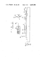
- FIG. 1 shows a conventional CCD output signal generating circuit
- FIG. 2 is a signal waveform diagram for explaining the operation of the CCD output signal generating circuit shown in FIG. 1;
- FIG. 3 is a circuit diagram of a correlated double sampling circuit used in the CCD output signal generating circuit shown in FIG. 1;
- FIGS. 4A and 4B show an example of the spectra of the noise components included in output signals of the output circuit and the correlated double sampling circuit used in the CCD output signal generating circuit shown in FIG. 1;
- FIG. 5 shows a CCD output signal generating circuit according to one embodiment of the present invention.
- FIG. 6 is a graph showing a level change of the noise components included in the output signal of the correlated double sampling circuit where the cut-off frequency of the low-pass filter used in the CCD output signal generating circuit shown in FIG. 5 is changed.
- FIG. 5 shows a CCD output signal generating circuit according to one embodiment of the present invention. Similar to the CCD output signal generating circuit shown in FIG. 1, the CCD output signal generating circuit of the invention comprises a CCD type charge transfer device 10 for transferring the signal charges in response to a drive signal of the frequency f c , an output circuit 21, and a correlated double sampling circuit 22.
- the CCD output signal generating circuit of FIG. 5 also has a low-pass filter circuit 31 connected between the output circuit 21 and the correlated double sampling circuit 22.
- the output circuit 21, correlated double sampling circuit 22, and low-pass filter circuit 31 cooperatively constitute a CCD output signal processing circuit 30.
- the inventor of the invention claimed herein has empirically examined the change in level of the noise component included in the output signal and generated from the correlated double sampling circuit 22 when the cut-off frequency of the low-pass filter circuit 31 is changed, from which examination the experimental result data shown in FIG. 6 was derived.
- the influence of the alias of the high frequency noise included in the output signal of the output circuit 21 increases when the cut-off frequency of the low-pass filter circuit 31 is set on high, so that there is a tendency for the noise component included in the output signal of the correlated double sampling circuit 22 to increase.
- the cut-off frequency of the low-pass filter circuit 31 when the cut-off frequency of the low-pass filter circuit 31 is set on low, for example, 0.5f c , it becomes difficult to separate the feed-through level set period RVP in the output signal of the output circuit 21 from the signal level set period SVP and, consequently, the noise component included in the output signal of the sampling circuit 22 increases.
- the cut-off frequency of the low-pass filter circuit 31 is gradually increased from, for instance, 0.5f c , the noise component from the correlated double sampling circuit 22 gradually decreases such that when the cut-off frequency is set to about 3f c , the noise component is minimized.
- the cut-off frequency is enlarged further, the noise component again increases.
- the cut-off frequency of the low-pass filter circuit 31 is set to a value which is two to six times, and, preferably, two and a half to four times as large as the frequency f c of the drive pulses ⁇ 1 to ⁇ 3 , the noise component included in the output signal from the correlated double sampling circuit 22 can be effectively suppressed.
- the synchronous noise and reset noise included in the output signal from the output circuit 21 are, apparently, similarily suppressed in the correlated double sampling circuit 22.
- the use of the CCD output signal generating circuit shown in FIG. 5 makes it possible to effectively suppress the noise that is caused due to the alias of the high frequency noise from the output circuit 21 as well as the synchronous noise and reset noise.
- the CCD output signal that accurately corresponds to the signal charges from the charge transfer device 10 can, therefore, be derived.
- the present invention has been described in the above with respect to one embodiment, the invention is not limited to only this embodiment.
- the correlated double sampling circuit 22 is constituted as shown in FIG. 3, in place of this it is also possible to use a correlated double sampling circuit which is constituted by, for example, two sample-hold circuits that are similar to the sample-hold circuit 230 shown in FIG. 3.
- a differential amplifier both for allowing the output signals corresponding to the reference and signal voltages from the output circuit 21 to be generated from these sample-hold circuits and for generating an output signal responsive to a difference between those output signals.
- the low-pass filter circuit 31 may be constituted by a resistor and a capacitor in a well known manner or by using both the resistance of a connection line connected between the circuits 21 and 22 and a capacitance connected to the connection line.
Landscapes
- Engineering & Computer Science (AREA)
- Microelectronics & Electronic Packaging (AREA)
- Power Engineering (AREA)
- Multimedia (AREA)
- Signal Processing (AREA)
- Physics & Mathematics (AREA)
- Ceramic Engineering (AREA)
- Condensed Matter Physics & Semiconductors (AREA)
- General Physics & Mathematics (AREA)
- Computer Hardware Design (AREA)
- Transforming Light Signals Into Electric Signals (AREA)
- Solid State Image Pick-Up Elements (AREA)
Applications Claiming Priority (2)
| Application Number | Priority Date | Filing Date | Title |
|---|---|---|---|
| JP59172746A JPH0669049B2 (ja) | 1984-08-20 | 1984-08-20 | Ccd出力信号処理回路 |
| JP59-172746 | 1984-08-20 |
Publications (1)
| Publication Number | Publication Date |
|---|---|
| US4683580A true US4683580A (en) | 1987-07-28 |
Family
ID=15947551
Family Applications (1)
| Application Number | Title | Priority Date | Filing Date |
|---|---|---|---|
| US06/763,225 Expired - Lifetime US4683580A (en) | 1984-08-20 | 1985-08-07 | CCD output signal processing circuit for use in an image pick-up device |
Country Status (4)
| Country | Link |
|---|---|
| US (1) | US4683580A (de) |
| EP (1) | EP0172474B1 (de) |
| JP (1) | JPH0669049B2 (de) |
| DE (1) | DE3576061D1 (de) |
Cited By (19)
| Publication number | Priority date | Publication date | Assignee | Title |
|---|---|---|---|---|
| US4803709A (en) * | 1986-08-29 | 1989-02-07 | Mitsubishi Denki Kabushiki Kaisha | Elimination of KTC noise in a charge coupled device |
| US5247554A (en) * | 1987-01-16 | 1993-09-21 | Kabushiki Kaisha Toshiba | Charge detection circuit |
| US5299032A (en) * | 1991-01-31 | 1994-03-29 | Sony Corporation | Image pick up apparatus |
| US5471515A (en) * | 1994-01-28 | 1995-11-28 | California Institute Of Technology | Active pixel sensor with intra-pixel charge transfer |
| US5473660A (en) * | 1994-06-01 | 1995-12-05 | U.S. Philips Corporation | Image sensing device |
| WO1996041464A1 (en) * | 1995-06-07 | 1996-12-19 | Ivp Integrated Vision Products Ab | Apparatus for reading and processing image information |
| US5600696A (en) * | 1995-10-11 | 1997-02-04 | David Sarnoff Research Center, Inc. | Dual-gain floating diffusion output amplifier |
| WO1997028558A2 (en) * | 1996-01-22 | 1997-08-07 | California Institute Of Technology | Active pixel sensor array with electronic shuttering |
| US5838176A (en) * | 1996-07-11 | 1998-11-17 | Foveonics, Inc. | Correlated double sampling circuit |
| US5844238A (en) * | 1996-03-27 | 1998-12-01 | David Sarnoff Research Center, Inc. | Infrared imager using room temperature capacitance sensor |
| US5946033A (en) * | 1996-05-28 | 1999-08-31 | Gatan, Inc. | Method and apparatus for multiple read-out speeds for a CTD |
| US5965871A (en) * | 1997-11-05 | 1999-10-12 | Pixart Technology, Inc. | Column readout multiplexer for CMOS image sensors with multiple readout and fixed pattern noise cancellation |
| US6021172A (en) * | 1994-01-28 | 2000-02-01 | California Institute Of Technology | Active pixel sensor having intra-pixel charge transfer with analog-to-digital converter |
| US6097432A (en) * | 1996-07-11 | 2000-08-01 | Synaptics, Inc. | Sense amplifier for high-density imaging array |
| US6392233B1 (en) | 2000-08-10 | 2002-05-21 | Sarnoff Corporation | Optomechanical radiant energy detector |
| US6421085B1 (en) | 1998-04-14 | 2002-07-16 | Eastman Kodak Company | High speed CMOS imager column CDS circuit |
| US6486503B1 (en) | 1994-01-28 | 2002-11-26 | California Institute Of Technology | Active pixel sensor array with electronic shuttering |
| US6940551B2 (en) | 2000-09-25 | 2005-09-06 | Foveon, Inc. | Active pixel sensor with noise cancellation |
| US20090195297A1 (en) * | 2008-01-31 | 2009-08-06 | Nec Electronics Corporation | Ccd device and method of driving same |
Families Citing this family (2)
| Publication number | Priority date | Publication date | Assignee | Title |
|---|---|---|---|---|
| US4914519A (en) * | 1986-09-19 | 1990-04-03 | Canon Kabushiki Kaisha | Apparatus for eliminating noise in a solid-state image pickup device |
| US5337893A (en) * | 1992-07-22 | 1994-08-16 | Electro Scientific Industries, Inc. | High capacity carrier plate |
Citations (6)
| Publication number | Priority date | Publication date | Assignee | Title |
|---|---|---|---|---|
| US4287441A (en) * | 1979-03-30 | 1981-09-01 | The United States Of America As Represented By The Secretary Of The Army | Correlated double sampling CCD video preprocessor-amplifier |
| US4293831A (en) * | 1979-03-30 | 1981-10-06 | Siemens Aktiengesellschaft | Monolithically integrated charge transfer circuit |
| US4309678A (en) * | 1979-02-02 | 1982-01-05 | Thomson-Csf | Sampling filter |
| US4488129A (en) * | 1981-09-25 | 1984-12-11 | Thomson-Csf | Device for current-reading of a quantity of electric charges and a charge-transfer filter equipped with said device |
| US4513260A (en) * | 1977-01-10 | 1985-04-23 | Texas Instruments Incorporated | Programmable frequency converting filter |
| US4528684A (en) * | 1982-07-23 | 1985-07-09 | Tokyo Shibaura Denki Kabushiki Kaisha | Charge-coupled device output circuit |
Family Cites Families (4)
| Publication number | Priority date | Publication date | Assignee | Title |
|---|---|---|---|---|
| US4048525A (en) * | 1975-09-02 | 1977-09-13 | General Electric Company | Output circuit for charge transfer transversal filter |
| JPS55105480A (en) * | 1979-02-07 | 1980-08-13 | Hitachi Ltd | Solid state pickup device |
| JPS5651166A (en) * | 1979-10-03 | 1981-05-08 | Hitachi Ltd | Solid image pickup device |
| US4435730A (en) * | 1982-03-08 | 1984-03-06 | Rca Corporation | Low noise CCD output |
-
1984
- 1984-08-20 JP JP59172746A patent/JPH0669049B2/ja not_active Expired - Lifetime
-
1985
- 1985-08-02 DE DE8585109724T patent/DE3576061D1/de not_active Expired - Lifetime
- 1985-08-02 EP EP85109724A patent/EP0172474B1/de not_active Expired
- 1985-08-07 US US06/763,225 patent/US4683580A/en not_active Expired - Lifetime
Patent Citations (6)
| Publication number | Priority date | Publication date | Assignee | Title |
|---|---|---|---|---|
| US4513260A (en) * | 1977-01-10 | 1985-04-23 | Texas Instruments Incorporated | Programmable frequency converting filter |
| US4309678A (en) * | 1979-02-02 | 1982-01-05 | Thomson-Csf | Sampling filter |
| US4287441A (en) * | 1979-03-30 | 1981-09-01 | The United States Of America As Represented By The Secretary Of The Army | Correlated double sampling CCD video preprocessor-amplifier |
| US4293831A (en) * | 1979-03-30 | 1981-10-06 | Siemens Aktiengesellschaft | Monolithically integrated charge transfer circuit |
| US4488129A (en) * | 1981-09-25 | 1984-12-11 | Thomson-Csf | Device for current-reading of a quantity of electric charges and a charge-transfer filter equipped with said device |
| US4528684A (en) * | 1982-07-23 | 1985-07-09 | Tokyo Shibaura Denki Kabushiki Kaisha | Charge-coupled device output circuit |
Non-Patent Citations (2)
| Title |
|---|
| "Stable Output Circuit for a Dynamic Shift Register", IBM Technical Disclosure Bulletin, vol. 18, No. 2, Jul. 1985, pp. 459-460. |
| Stable Output Circuit for a Dynamic Shift Register , IBM Technical Disclosure Bulletin, vol. 18, No. 2, Jul. 1985, pp. 459 460. * |
Cited By (30)
| Publication number | Priority date | Publication date | Assignee | Title |
|---|---|---|---|---|
| US4803709A (en) * | 1986-08-29 | 1989-02-07 | Mitsubishi Denki Kabushiki Kaisha | Elimination of KTC noise in a charge coupled device |
| US5247554A (en) * | 1987-01-16 | 1993-09-21 | Kabushiki Kaisha Toshiba | Charge detection circuit |
| US5299032A (en) * | 1991-01-31 | 1994-03-29 | Sony Corporation | Image pick up apparatus |
| US6486503B1 (en) | 1994-01-28 | 2002-11-26 | California Institute Of Technology | Active pixel sensor array with electronic shuttering |
| US20030160238A1 (en) * | 1994-01-28 | 2003-08-28 | California Institute Of Technology, A California Corporation | Active pixel sensor with intra-pixel charge transfer |
| US7105371B2 (en) | 1994-01-28 | 2006-09-12 | California Institute Of Technology | Method of acquiring an image from an optical structure having pixels with dedicated readout circuits |
| US20040160522A1 (en) * | 1994-01-28 | 2004-08-19 | California Institute Of Technology | Active pixel sensor with intra-pixel charge transfer |
| US6744068B2 (en) | 1994-01-28 | 2004-06-01 | California Institute Of Technology | Active pixel sensor with intra-pixel charge transfer |
| US6665013B1 (en) * | 1994-01-28 | 2003-12-16 | California Institute Of Technology | Active pixel sensor having intra-pixel charge transfer with analog-to-digital converter |
| US5471515A (en) * | 1994-01-28 | 1995-11-28 | California Institute Of Technology | Active pixel sensor with intra-pixel charge transfer |
| US6101232A (en) * | 1994-01-28 | 2000-08-08 | California Institute Of Technology | Active pixel sensor with intra-pixel charge transfer |
| US6021172A (en) * | 1994-01-28 | 2000-02-01 | California Institute Of Technology | Active pixel sensor having intra-pixel charge transfer with analog-to-digital converter |
| US5473660A (en) * | 1994-06-01 | 1995-12-05 | U.S. Philips Corporation | Image sensing device |
| WO1996041464A1 (en) * | 1995-06-07 | 1996-12-19 | Ivp Integrated Vision Products Ab | Apparatus for reading and processing image information |
| US6313876B1 (en) | 1995-06-07 | 2001-11-06 | Ivp Integrated Vision Products Ab Teknikringen | Sensor element array for reading and processing image information |
| US5600696A (en) * | 1995-10-11 | 1997-02-04 | David Sarnoff Research Center, Inc. | Dual-gain floating diffusion output amplifier |
| WO1997014153A1 (en) * | 1995-10-11 | 1997-04-17 | Sarnoff Corporation | Dual-gain floating diffusion output amplifier |
| WO1997028558A2 (en) * | 1996-01-22 | 1997-08-07 | California Institute Of Technology | Active pixel sensor array with electronic shuttering |
| WO1997028558A3 (en) * | 1996-01-22 | 1997-10-02 | California Inst Of Techn | Active pixel sensor array with electronic shuttering |
| US5844238A (en) * | 1996-03-27 | 1998-12-01 | David Sarnoff Research Center, Inc. | Infrared imager using room temperature capacitance sensor |
| US6249001B1 (en) | 1996-03-27 | 2001-06-19 | Sarnoff Corporation | Infrared imager using room temperature capacitance sensor |
| US5946033A (en) * | 1996-05-28 | 1999-08-31 | Gatan, Inc. | Method and apparatus for multiple read-out speeds for a CTD |
| US5838176A (en) * | 1996-07-11 | 1998-11-17 | Foveonics, Inc. | Correlated double sampling circuit |
| US6097432A (en) * | 1996-07-11 | 2000-08-01 | Synaptics, Inc. | Sense amplifier for high-density imaging array |
| US5965871A (en) * | 1997-11-05 | 1999-10-12 | Pixart Technology, Inc. | Column readout multiplexer for CMOS image sensors with multiple readout and fixed pattern noise cancellation |
| US6421085B1 (en) | 1998-04-14 | 2002-07-16 | Eastman Kodak Company | High speed CMOS imager column CDS circuit |
| US6392233B1 (en) | 2000-08-10 | 2002-05-21 | Sarnoff Corporation | Optomechanical radiant energy detector |
| US6940551B2 (en) | 2000-09-25 | 2005-09-06 | Foveon, Inc. | Active pixel sensor with noise cancellation |
| US20090195297A1 (en) * | 2008-01-31 | 2009-08-06 | Nec Electronics Corporation | Ccd device and method of driving same |
| US7872521B2 (en) * | 2008-01-31 | 2011-01-18 | Renesas Electronics Corporation | CCD device and method of driving same |
Also Published As
| Publication number | Publication date |
|---|---|
| EP0172474A3 (en) | 1987-09-16 |
| EP0172474A2 (de) | 1986-02-26 |
| JPH0669049B2 (ja) | 1994-08-31 |
| DE3576061D1 (de) | 1990-03-22 |
| JPS6150365A (ja) | 1986-03-12 |
| EP0172474B1 (de) | 1990-02-14 |
Similar Documents
| Publication | Publication Date | Title |
|---|---|---|
| US4683580A (en) | CCD output signal processing circuit for use in an image pick-up device | |
| US4287441A (en) | Correlated double sampling CCD video preprocessor-amplifier | |
| US4823027A (en) | Sample and hold circuit | |
| US5434620A (en) | Image sensor | |
| US6025875A (en) | Analog signal sampler for imaging systems | |
| US4255715A (en) | Offset correction circuit for differential amplifiers | |
| US5796361A (en) | CCD signal digitizing integrated circuit | |
| JPS5919297A (ja) | 電荷結合装置の出力回路 | |
| US4570080A (en) | Corrected sample-and-hold circuit | |
| JPH0346918B2 (de) | ||
| US3696305A (en) | High speed high accuracy sample and hold circuit | |
| EP0289191B1 (de) | Signalleseschaltung | |
| US5801555A (en) | Correlative double sampling (CDS) device | |
| EP0312142B1 (de) | Ausleseschaltung einer Verzögerungsschaltung | |
| GB2111780A (en) | Improvements in or relating to amplifier systems | |
| JPS6069969A (ja) | イメ−ジセンサ | |
| US5467130A (en) | Ground driven delay line correlator | |
| JP3064703B2 (ja) | サンプルホールド回路 | |
| US4455666A (en) | Compensation of 1st order transfer inefficiency effect in a C.T.D. | |
| US6055016A (en) | L-C low pass filter correlator | |
| JPH04345277A (ja) | 電圧ホールド回路 | |
| US4635115A (en) | Synchronous separation circuit | |
| US4800579A (en) | Charge transfer device provided with charge detection circuit of a floating gate system | |
| CA2073958C (en) | Phase shift sample-and-hold circuit for determining the mean amplitude for periodic pulses | |
| JP2764808B2 (ja) | ccdデータをデジタル化する方法及び装置 |
Legal Events
| Date | Code | Title | Description |
|---|---|---|---|
| AS | Assignment |
Owner name: KABUSHIKI KAISHA TOSHIBA, 72 HORIKAWA-CHO, SAIWAI- Free format text: ASSIGNMENT OF ASSIGNORS INTEREST.;ASSIGNOR:MATSUNAGA, YOSHIYUKI;REEL/FRAME:004443/0480 Effective date: 19850722 |
|
| STCF | Information on status: patent grant |
Free format text: PATENTED CASE |
|
| FPAY | Fee payment |
Year of fee payment: 4 |
|
| FEPP | Fee payment procedure |
Free format text: PAYOR NUMBER ASSIGNED (ORIGINAL EVENT CODE: ASPN); ENTITY STATUS OF PATENT OWNER: LARGE ENTITY |
|
| FPAY | Fee payment |
Year of fee payment: 8 |
|
| FPAY | Fee payment |
Year of fee payment: 12 |