US4634043A - Engaging second articles to engaged first articles - Google Patents
Engaging second articles to engaged first articles Download PDFInfo
- Publication number
- US4634043A US4634043A US06/652,388 US65238884A US4634043A US 4634043 A US4634043 A US 4634043A US 65238884 A US65238884 A US 65238884A US 4634043 A US4634043 A US 4634043A
- Authority
- US
- United States
- Prior art keywords
- article
- chip
- engaged
- workpiece
- pockets
- Prior art date
- Legal status (The legal status is an assumption and is not a legal conclusion. Google has not performed a legal analysis and makes no representation as to the accuracy of the status listed.)
- Expired - Lifetime
Links
Images

Classifications
-
- H—ELECTRICITY
- H01—ELECTRIC ELEMENTS
- H01L—SEMICONDUCTOR DEVICES NOT COVERED BY CLASS H10
- H01L21/00—Processes or apparatus adapted for the manufacture or treatment of semiconductor or solid state devices or of parts thereof
- H01L21/67—Apparatus specially adapted for handling semiconductor or electric solid state devices during manufacture or treatment thereof; Apparatus specially adapted for handling wafers during manufacture or treatment of semiconductor or electric solid state devices or components ; Apparatus not specifically provided for elsewhere
- H01L21/67005—Apparatus not specifically provided for elsewhere
- H01L21/67011—Apparatus for manufacture or treatment
- H01L21/67144—Apparatus for mounting on conductive members, e.g. leadframes or conductors on insulating substrates
-
- B—PERFORMING OPERATIONS; TRANSPORTING
- B23—MACHINE TOOLS; METAL-WORKING NOT OTHERWISE PROVIDED FOR
- B23K—SOLDERING OR UNSOLDERING; WELDING; CLADDING OR PLATING BY SOLDERING OR WELDING; CUTTING BY APPLYING HEAT LOCALLY, e.g. FLAME CUTTING; WORKING BY LASER BEAM
- B23K3/00—Tools, devices, or special appurtenances for soldering, e.g. brazing, or unsoldering, not specially adapted for particular methods
- B23K3/08—Auxiliary devices therefor
Definitions
- This invention relates to removably engaging a first article and then engaging a second article to the engaged first article. More particularly, this invention relates to expedients such as a head for removably engaging a solid state chip of the type to be bonded to a heated substrate and then engaging to the chip, a workpiece of material typically liquefied by heat for the bonding.
- One of the most popular methods of assembling parts without mechanical fasteners is to join surfaces of the respective parts with an intermediate substance, sometimes called a bonding material.
- a bonding material sometimes called a bonding material
- the types discussed in this application are those which are liquefied by heat for the bonding.
- a problem is to select a bonding material and apply the same to suit a method by which parts are assembled to acquire joints having desired characteristics.
- a challenging task is to bond an often delicate, electronic chip with precise registration to a substrate and with a joint having good conductivity of electricity and operating heat.
- a problem is to liquefy and uniformly distribute the bonding material over the surfaces to be joined.
- Another problem is to obtain a uniform and desired reaction time over the joint and between the bonding material and the surface metals.
- a desirable method of achieving uniform distribution is to first form a solid workpiece of bonding material (called a "preform") and place the same between cold surfaces prior to any heating. Such method assures a uniform and desired reaction time providing heat is uniformly applied and uniformly and timely removed. Oxidation of surfaces and bonding material at elevated temperatures is mitigated because the cold joining tends to mitigate air in a joint during a later heating step.
- a problem is that uniform heating is often done in a chamber away from an assembly station. Many electronic chip assemblies are so tiny, precise and delicate that clamping and moving steps risk damage to chips and their respective registration to substrates.
- Uniform heating at an assembly station is often achieved by heating a substrate (rather than a vulnerable chip).
- a problem is to control liquefication of a preform of bonding material while the preform and a chip are being registered to a site on a substrate. If heat is avoided until after registration of the preform and chip, respectively, an unacceptable waiting period is experienced during the heating step. If the heat is applied before registration, the preform liquefies and oxidizes while the chip is being registered to the preform.
- Expedients including heads are provided for removably engaging a first article having peripheral sides, such as a chip, and then engaging to the engaged chip, a second article, such as a workpiece of bonding material. Such engaged articles may then be simultaneously registered for bonding the chip via the bonding material to a site on a heated substrate.
- a body has an upper portion adapted for support and a lower portion terminating in a downwardly presented working face.
- Such working face may have flat, smooth surfaces for receiving the chip.
- the working face has a vacuum cavity formed by a plurality of inwardly and upwardly directed surfaces for engaging and positioning the chip such that at least a portion of the peripheral sides protrude from the working face.
- a vacuum bore in the body is adapted for a first connection between a vacuum source and the working face for removably engaging the chip and for holding the same against the engaging surfaces.
- expedients are provided for moving air streams toward the working face at the peripheral sides of the engaged chip.
- pockets having a second connection to a vacuum source may be provided to move air at or intermediate the corners at the periphery of an engaged chip.
- the streams of air into the pockets are sufficient in force, direction and distribution around the peripheral sides to engage a free workpiece of bonding material.
- the air streams capture sufficient peripheral portions of the workpiece to engage and hold such workpiece against the chip. Then the chip and workpiece may be simultaneously registered to a site for operations such as bonding.
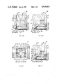
- FIG. 1 is an elevation view of a prior art head adapted for registering a chip to a workpiece of bonding material which has been previously applied to a heated substrate according to the prior art;
- FIG. 2 is a bottom view of the head shown in FIG. 1 revealing features of a working face
- FIG. 3 is an elevation view of a head adapted for removably engaging a chip and then engaging a workpiece to the chip prior to registering either article to a heated substrate in accordance with an embodiment of the invention
- FIG. 4 is a bottom view of the head shown in FIG. 3 revealing features in a working face including pockets at chip corners for moving and directing air streams in accordance with an embodiment of the invention
- FIG. 5A is a greatly enlarged, partial view in section of the head shown in FIG. 4, taken along line 5--5, depicting air streams drawn from first and second vacuum connections in accordance with an embodiment of the invention
- FIG. 5B is similar to FIG. 5A, but air streams are drawn from only a first vacuum connection in accordance with an embodiment of the invention
- FIG. 6 is a bottom view of a head having pockets located intermediate of the chip corners in accordance with the invention.
- FIG. 7 is a greatly enlarged sectional view of the head shown in FIG. 6, taken along line 7--7, depicting air streams drawn from a first vacuum connection through pockets and a vacuum bore in accordance with an embodiment of the invention.
- FIGS. 1-7 show solidly or in outline, a typical first article 10 which may be removably engaged in the practice of the invention.
- removably engaged it is meant that an article may be drawn against, or otherwise attracted and held to, apparatus such as a pickup head. While so engaged, the article may be manipulated with the head and readily disengaged for fixed or free placement in an assembly or on a substrate.
- FIG. 2 the same figures show solidly or in outline, a typical second article 35 which may be engaged to an engaged first article 10 in the practice of the invention.
- the first article 10 will now be described followed by the prior art pickup heads and the second articles 35.
- Chip 10 may include a PIN photodiode which generates electrical signals in fast response to received radiation such as light pulses from a source (not shown).
- Chip 10 may typically be constructed of III-V compounds as set forth in the Periodic Table of Elements.
- chip 10 may contain a binary, InP substrate of a type which is transparent to a desired wavelength of radiation.
- a ternary, InGaAs intrinsic layer may be grown on the substrate for electron-hole generation by the radiation.
- a diffused P doped region may communicate between the intrinsic layer and a metallized contact 11 on a top, major surface 12 of chip 10.
- an N doped region may communicate between the intrinsic layer and a metallized, frame-shaped contact 13 on a bottom, major surface 14 of chip 10.
- the diode may be reverse-biased, creating an electric field across the intrinsic layer.
- Chip 10 may be as little as about 0.023 inches (0.6 mm) square by about 0.004 inches (0.1 mm) thick and have rectangular sides 16 which are substantially uniform in size, shape and surface texture.
- the major surfaces 12 and 14 are closely parallel to one another and the peripheral sides 16 are substantially perpendicular to the major surfaces.
- a head 18 is shown (in an elevation view in FIG. 1 and in a bottom view in FIG. 2) for pickup and placement of articles such as a semiconductor chip 10. Head 18 is especially advantageous for such work because contact to the major surfaces 12 and 14 is avoided, stresses applied to the described chip structure are low and orientation of chip 10 is effectively controlled.
- Head 18 has a cylindrical body 19 which may be about 0.063 inches (1.6 mm) in diameter by about 0.75 inches (19.0 mm) long, but much of the body cannot be shown in FIGS. 1 and 2 because of the large scale of the figures.
- Body 19 has an upper portion (not shown) which is adapted for support and a lower portion terminating in a downwardly presented working face 21 best seen in FIG. 2. From the periphery of body 19 to the working face 21, tapered surfaces 22 are provided which in this case are uniform in dimension because working face 19 is adapted to handle square chips 10.
- Surfaces 22 are usually provided by grinding because body 19 is typically made of a very hard material such as heat treated steel, ceramic, titanium carbide or tungsten carbide to resist wear from the articles which are engaged to head 18.
- a cavity 24 is formed by four uniformly dimensioned walls 25 having four uniformly dimensioned, inwardly and upwardly inclined surfaces 26.
- Surfaces 26 are for engaging corresponding top edges of sides 16 of a chip 10.
- Surfaces 26 are converged to a bore 28 extending through the body 19 and adapted for connection to a vacuum source (not shown) to draw air according to arrow 40 (FIG. 1).
- the diameter of bore 28 be adequate to pass air flow during engaging a chip 10 and that the vacuum source be of sufficient strength and air moving capacity to hold chip 10 while it is registered by head 18.
- the illustrative chip 10 and head 18 that bore 28 be about 0.006 inch (0.15 mm) in diameter and that a vacuum source pass about 0.02-0.12 CFM of air while holding vacuum at about 5 psia.
- bore 28 is small because chip 10 is light in weight and seats well in cavity 24 with few and small clearance spaces to pass air. It will be appreciated that the illustrative head 18, with its ancillary features does a fine job of securing a chip 10 until it is registered on a site on a substrate.
- FIG. 1 shows a typical substrate 30, also referred to herein as a thin slab 30, (which may be made of alumina ceramic, beryl mineral or silicon) having a central opening 31.
- a thin slab 30 which may be made of alumina ceramic, beryl mineral or silicon
- the slab 30 may be erected and so oriented that a beam of light will pass into opening 31 and into the active region 15 of chip 10.
- a site 32 for bonding is provided by a contact layer of gold (also designated by the numeral 32) extending to a circuit (not shown) to process signals generated in chip 10.
- the contacts 11 and 13 on chip 10 typically have gold metalization so oxidation is not a problem at room temperatures.
- the III-V construction of a chip 10 is known to be brittle and weak, especially in tiny, thin shapes. Consequently, a gentle bonding method is indicated which minimizes residual stresses in a chip 10 and a bonded joint.
- the joint should be highly conductive of operating electricity and heat from chip 10 to the conductive site 32 on the substrate 30.
- a bonding material such as an alloy containing, by weight, 12% Ge and 88% Au which melts sharply and uniformly at about 356° C. and is compatible with the metals of contact 13 on chip 10 and the layer 32 on substrate 30.
- Such bonding material is initially formed from a bulk source (not shown) and typically punched into a preformed article to suit chip 10 and the bonding site 32.
- a preformed article is the second article 35 which will also be referred to as a workpiece 35.
- Workpiece 35 may be about 0.034 inch (0.86 mm) outside diameter by about 0.018 inch (0.46 mm) inside diameter by about 0.001 inch (0.025 mm) thick and have major surfaces 36 and 37. Workpiece 35 is broader than chip 10 along chip sides 16 and such broader peripheral portions are designated by the numeral 38. Such a workpiece 35 is placed in a joint to achieve uniform distribution of bonding material over joining surfaces and to mitigate oxidation by mitigating air presence at surfaces 36 and 37 at high temperatures.
- Heating the workpiece 35 to achieve liquidation of bonding material has been a problem when such microminiature articles 10 and 35 are involved and precise registration to a site 32 is desired.
- heater 33 was sometimes activated to heat substrate 30 while head 18 was manipulated to bring its working face 21 with a chip 10 close to the site 32.
- head 18 was manipulated to bring its working face 21 with a chip 10 close to the site 32.
- a race was on to register chip 10 (according to arrow 39) before workpiece 35 was liquified and/or oxidized.
- workpiece 35 or chip 10 or both were often improperly registered and an ensuing joint sometimes had substandard conductivity characteristics.
- FIG. 3 is an elevation view and FIG. 4 is a bottom view of an improved head 45 for successively engaging an article 10 and 35, respectively, and for registering the same to a site 32 on a substrate 30 in accordance with one embodiment of the invention.
- Head 45 has features similar to head 18 for similar functions and new features for new functions.
- Head 45 includes a cylindrical body 46 having dimensions and materials of construction similar to body 19 of head 18. An upper portion (not shown) is adapted for support and a lower portion of body 46 terminates in a downwardly presented working face 48 best seen in FIG. 4. Because head 45 is adapted for engaging a square chip 10, many corresponding features of body 46 and face 48 are uniform in dimensions and shape. For example, tapered surfaces 52 are provided (such as by grinding) from the periphery of body 46 to a cavity 54 formed by four walls 55 having four similar, inwardly and upwardly inclined surfaces 56. Surfaces 56 are for engaging corresponding top edges of sides 16 of a chip 10. Surfaces 56 converge to a first bore 58 extending through the body 46 and adapted for a first connection to a vacuum source (not shown) for moving air according to arrow 59 which will be explained later.
- working face 48 is made wider than working face 21 to accommodate in cavity 54 a plurality of pockets 60 located as best seen in FIG. 4. Pockets 60 are provided in the corners of cavity 54 roughly centered at the corners of a chip 10 when such chip is engaged to head 45.
- head 45 is provided with pockets 60 for exactly the opposite purpose.
- the pockets 60 are provided to move (or to permit movement of) air streams toward working face 48 at the peripheral sides 16 of a chip 10 when said chip is engaged in cavity 24.
- Such air streams should be sufficient in force, direction and distribution around sides 16 that when head 45 moves an engaged chip 10 adjacent to a free workpiece 35, said workpiece becomes engaged as shown in FIG. 3.
- the air streams produce sufficient force adjacent peripheral portions, e.g., portions 38, of workpiece 35 that the workpiece is engaged and held against the chip 10.
- the air streams are found to have sufficient force for a workpiece 35 when about 0.06 to about 0.12 CFM of air is moved through the pockets 60 and the streams are confined along the sides 16 of a chip 10 as shown in FIG. 3.
- the air streams are found to be sufficient in direction when they are directed substantially vertically along the sides 16 of an engaged chip 10. Sufficient distribution of the air streams is obtained for chip 10 and workpiece 35 when ones of pockets 60 are located at each corner of an engaged chip 10 as shown in FIGS. 3 and 4.
- the pockets 60 are about 0.007 inch (0.18 mm) in diameter and about 0.010 inch (0.25 mm) deep, measured from the bottom surface of a wall 55.
- Such pockets may be conveniently provided in a tungsten carbide body 46 by electrical discharge methods of cutting.
- a wire electrode may be at a first polarity from a power source (not shown) and body 46 may be at a second polarity to complete a circuit to such source.
- a wire electrode may be at a first polarity from a power source (not shown) and body 46 may be at a second polarity to complete a circuit to such source.
- Such work is often done in an oil bath for heat control.
- the word "pockets" is used to describe recessed features for controlling air streams and reflect the appearance of the recessed features shown in the figures. Nevertheless, it is to be understood that the invention is not limited to the recessed features shown.
- Features such as ducts, holes, apertures, channels and similar recesses or conduits with or without directional devices such as vanes may be equally effective in moving (or controlling movement) of air streams.
- the embodiment illustrated in FIG. 3 utilizes only a first vacuum connection to bore 58 to move the air streams.
- ducts 62 shown in phantom lines
- the first and second connections made be made to the same or separate vacuum sources.
- Such source or sources can readily be adapted to provide adequate air moving capacity and a vacuum pressure (i.e., well below 14.7 psia) suitable for the engaging.
- head 45 When proper pockets 60, adequate vacuum and good connections are provided, head 45 will readily, removably engage a chip 10 as shown in FIG. 3. Moreover, head 45 will also then readily engage an adjacent, free workpiece 35, also shown in FIG. 3. Relative motion is then produced between head 45 and a heated substrate 30, but the workpiece 35 is held away from the heat in a solid, unoxidized state and engaged to chip 10 until contact is made to substrate 30 by such motion according to arrow 65. Then the workpiece 35 of bonding material liquefies substantially without the presence of air to contacts 13 and 32.
- the substrate 30, including the registered articles 10 and 35 may subsequently be cooled such as by gas from a tube 66 connected to as gas source (not shown). Alternatively, the power to heater 33 may be deactivated, the substrate may be moved or both, to achieve cooling and complete a bond of chip 10 to site 32 on substrate 30.
- FIGS. 5A and 5B show in greater detail, two methods of moving air streams in the practice of various embodiments of the invention.
- the partial views are both assumed to be taken along line 5--5 in FIG. 4.
- the head in FIG. 5A will be assumed to be a head 45, with ducts 62 provided and the head in FIG. 5B will be assumed to be a head 45, without ducts 62.
- FIG. 5A depicts, for ease of description, air streams 68 and 69 as though a body of moving air can be divided into discrete portions.
- Such streams 68 and 69 originate at walls 55 and adjacent to sides 16 and lower surface 14 of a chip 10.
- Streams 68 are drawn into pockets 60, through ducts 62 and second connections to a vacuum source (which could be common) according to arrow 64.
- Streams 69 are drawn into pockets 60, through apertures 70, cavity 54, the bore 58 and a first connection to a vacuum source (which could be the common source) according to arrow 72.
- the four pockets 60 pass a total of about 0.20 CFM of air. About 60 to 80% is passed through the ducts 62 and about 20 to 40% is passed into apertures 70 and through the bore 58.
- Such information is offered by way of explaining the requirements and sizes of pockets 60, ducts 62, the bore 58 and a vacuum source and not by way of limiting the invention.
- the air streams operate to engage the second article 35.
- the air streams lower the air pressure between walls 55 and the sides 16 and draw portions 38 of the workpiece 35 toward the working face 48.
- such drawing is accompanied by a lowering of air pressure under chip 10 by air streams 69 moving over surface 14, a phenomena known as the "Coanda" effect.
- Such effect would explain an observed snapping action by workpiece 35 against chip 10 which is enhanced by movement of air through the open center portion of workpiece 35 just prior to engagement.
- Another explanation is that the flow of air at the periphery of chip 10 simply engulfs peripheral portions 38 (and others) of workpiece 35 and draws the workpiece against chip 10.
- the portions 38 do not significantly protrude away from chip 10 at chip corners. Since section 5--5 is taken at such corners, the corner regions are seen to have better access for air than the sides regions and the air streams 68 and 69 follow the paths shown in FIG. 5A.
- FIG. 5B A presently preferred method of moving air streams through pockets 60 in a head 45 is shown in FIG. 5B.
- Air streams 74 are depicted, originating at walls 55 and adjacent to sides 16 and the lower surface 14 of a chip 10. Streams 74 are drawn into the pockets 60, through apertures 70, cavity 54, the first bore 58 and a first connection to a vacuum source according to arrow 59.
- the pockets 60 are located partially outward and partially inward of the periphery of an engaged chip 10. Also, the pockets 60 are of such width and depth that the inward portion of a pocket opens into and communicates with the vacuum cavity 54 through apertures 70.
- the bore 58 aids in moving air when ducts 62 are utilized as in FIG. 5A. Even more advantageous, such construction permits bore 58 (and a first vacuum connection to a source for holding chip 10) to communicate with the pockets 60 and move air streams 74 to engage workpiece 35 (FIG. 5B) without the ducts 62.
- FIGS. 6 and 7 illustrate still another embodiment of the invention including a head 75 having a body 76 much like the body 46 of head 45.
- Other features are similar to those of head 45.
- a working surface 78, tapered surfaces 82, cavity 84, walls 85, engaging surfaces 86 and bore 88 are similar in form and function to respective working surface 48, tapered surfaces 52, cavity 54, walls 55, surfaces 56 and the bore 58 of head 45.
- pockets 60 for moving, directing and distributing air streams are located at the sides 16 of a chip 10, i.e., at positions intermediate chip corners. Such locations are advantageous for some applications because portions 38 of the workpiece 35 are more prominent at the natural center lines 91 and 92 of head 75. Accordingly, the air streams have more of workpiece 35 to engulf and grasping an article 35 is more efficient.
- FIG. 7 depicts air streams 93 moving through the pockets 90 in a head 75 for engaging first and then second articles.
- Air streams 93 originate between walls 85 and adjacent to the sides 16 and lower surfaces 14 of a chip 10 (as in FIG. 5A) and pass to a vacuum source according to arrow 95.
- Each aperture 94 in head 75 is larger than an aperture 70 shown in head 45 in FIGS. 5A and 5B.
- the passageways for air streams 93 moving between walls 85 and portions 38 of workpiece 35 are much smaller than those for head 45. Consequently, head 75 does an excellent job of engaging and holding workpiece 35 while passing less air than head 45.
- ducts 96 may be provided, having second connections to a vacuum source for passing air according to arrow 97, to serve the pockets 90.
- workpiece 35 has edge portions 38 which protrude from peripheral sides of the chip 10 and such portions are engaged by the air streams. Also, it is seen in the figures that workpiece 35 is a substantially flat article. However, it is found that workpiece 35 need not be broader than chip 10 nor need such workpiece be flat. It is sufficient that workpiece 35 be of a conventional size for preformed bonding materials, i.e., that the workpiece be about as broad as, and roughly conform to, the article to be bonded.
- PIN chip 10 has been selected for illustration and description, it is to be understood that the invention is not so limited. Many of the problems seen in using a preform to bond chip 10 to a substrate 30 are similar to, although more difficult than, the problems seen in bonding other solid state chips which may also be handled and bonded according to the invention. Also, the invention is not limited to square or rectangular chips or even to solid state chips. Article 10 could as well be a disc-like article or any other article having peripheral sides along which air streams could be moved to engage a second article.
Landscapes
- Engineering & Computer Science (AREA)
- Mechanical Engineering (AREA)
- Physics & Mathematics (AREA)
- Condensed Matter Physics & Semiconductors (AREA)
- General Physics & Mathematics (AREA)
- Manufacturing & Machinery (AREA)
- Computer Hardware Design (AREA)
- Microelectronics & Electronic Packaging (AREA)
- Power Engineering (AREA)
- Wire Bonding (AREA)
Abstract
Description
Claims (6)
Priority Applications (1)
| Application Number | Priority Date | Filing Date | Title |
|---|---|---|---|
| US06/652,388 US4634043A (en) | 1984-09-20 | 1984-09-20 | Engaging second articles to engaged first articles |
Applications Claiming Priority (1)
| Application Number | Priority Date | Filing Date | Title |
|---|---|---|---|
| US06/652,388 US4634043A (en) | 1984-09-20 | 1984-09-20 | Engaging second articles to engaged first articles |
Publications (1)
| Publication Number | Publication Date |
|---|---|
| US4634043A true US4634043A (en) | 1987-01-06 |
Family
ID=24616644
Family Applications (1)
| Application Number | Title | Priority Date | Filing Date |
|---|---|---|---|
| US06/652,388 Expired - Lifetime US4634043A (en) | 1984-09-20 | 1984-09-20 | Engaging second articles to engaged first articles |
Country Status (1)
| Country | Link |
|---|---|
| US (1) | US4634043A (en) |
Cited By (14)
| Publication number | Priority date | Publication date | Assignee | Title |
|---|---|---|---|---|
| US4787548A (en) * | 1987-07-27 | 1988-11-29 | Pace Incorporated | Nozzle structure for soldering and desoldering |
| EP0300873A1 (en) * | 1987-07-24 | 1989-01-25 | Thomson Composants Militaires Et Spatiaux | Soldering furnace for integrated-circuit chips |
| EP0305695A2 (en) * | 1987-08-31 | 1989-03-08 | Siemens Aktiengesellschaft | Soldering head for receiving and adjusting elements during soldering and unsoldering, especially for surface mounted elements (SMD) |
| US4844325A (en) * | 1987-03-18 | 1989-07-04 | Sumitomo Electric Industries, Ltd. | Method and apparatus for die-bonding semiconductor chip bonding |
| EP0329823A2 (en) * | 1988-02-22 | 1989-08-30 | E.I. Du Pont De Nemours And Company | Die attach pickup tools |
| US4972990A (en) * | 1988-02-22 | 1990-11-27 | Pace Incorporated | Apparatus for removal and installing electronic components with respect to a substrate |
| EP0529953A1 (en) * | 1991-08-29 | 1993-03-03 | AT&T Corp. | Placement and bonding technique |
| EP0542444A1 (en) * | 1991-11-04 | 1993-05-19 | AT&T Corp. | Method and apparatus for bonding a plurality of optical elements |
| US5392771A (en) * | 1990-10-19 | 1995-02-28 | Uwatec Ag | Underwater monitoring and communication system |
| EP0669642A2 (en) * | 1994-01-31 | 1995-08-30 | Applied Materials, Inc. | Apparatus and methods for processing substrates |
| EP0852983A1 (en) * | 1997-01-08 | 1998-07-15 | Esec Sa | Brazing parts forming device used for soft soldering of semiconductor chips |
| US6179196B1 (en) * | 1995-08-14 | 2001-01-30 | International Business Machines Corporation | Apparatus for manufacturing circuit boards |
| US6321971B1 (en) * | 1997-10-22 | 2001-11-27 | Samsung Electronics Co., Ltd. | Die collet for a semiconductor chip and apparatus for bonding semiconductor chip to a lead frame |
| US20140027068A1 (en) * | 2012-07-30 | 2014-01-30 | Kin Yik Hung | Bond head for thermal compression die bonding |
Citations (10)
| Publication number | Priority date | Publication date | Assignee | Title |
|---|---|---|---|---|
| US3458102A (en) * | 1967-08-09 | 1969-07-29 | Kulicke & Soffa Ind Inc | Semiconductor wafer pickup and bonding tool |
| US3568307A (en) * | 1969-04-10 | 1971-03-09 | Kulicke & Soffa Ind Inc | Method of picking up and bonding semiconductor wafers to a carrier |
| US3584859A (en) * | 1969-01-03 | 1971-06-15 | Robert E Siron | Vacuum-operated specimen-holding device |
| US3676911A (en) * | 1970-11-12 | 1972-07-18 | Frank C Austin | Holding tool |
| US3695502A (en) * | 1970-09-14 | 1972-10-03 | Floyd E Gaiser | Bonding tool |
| US3873144A (en) * | 1973-06-28 | 1975-03-25 | John C Diepeveen | Die holding tool and method of using same |
| JPS5680141A (en) * | 1979-12-04 | 1981-07-01 | Seiko Epson Corp | Manufacture device of semiconductor |
| US4295596A (en) * | 1979-12-19 | 1981-10-20 | Western Electric Company, Inc. | Methods and apparatus for bonding an article to a metallized substrate |
| JPS57104220A (en) * | 1980-12-22 | 1982-06-29 | Toshiba Corp | Wafer fixing apparatus |
| WO1982002235A1 (en) * | 1979-12-26 | 1982-07-08 | Associates Varian | Planar vacuum seal for isolating an air bearing |
-
1984
- 1984-09-20 US US06/652,388 patent/US4634043A/en not_active Expired - Lifetime
Patent Citations (10)
| Publication number | Priority date | Publication date | Assignee | Title |
|---|---|---|---|---|
| US3458102A (en) * | 1967-08-09 | 1969-07-29 | Kulicke & Soffa Ind Inc | Semiconductor wafer pickup and bonding tool |
| US3584859A (en) * | 1969-01-03 | 1971-06-15 | Robert E Siron | Vacuum-operated specimen-holding device |
| US3568307A (en) * | 1969-04-10 | 1971-03-09 | Kulicke & Soffa Ind Inc | Method of picking up and bonding semiconductor wafers to a carrier |
| US3695502A (en) * | 1970-09-14 | 1972-10-03 | Floyd E Gaiser | Bonding tool |
| US3676911A (en) * | 1970-11-12 | 1972-07-18 | Frank C Austin | Holding tool |
| US3873144A (en) * | 1973-06-28 | 1975-03-25 | John C Diepeveen | Die holding tool and method of using same |
| JPS5680141A (en) * | 1979-12-04 | 1981-07-01 | Seiko Epson Corp | Manufacture device of semiconductor |
| US4295596A (en) * | 1979-12-19 | 1981-10-20 | Western Electric Company, Inc. | Methods and apparatus for bonding an article to a metallized substrate |
| WO1982002235A1 (en) * | 1979-12-26 | 1982-07-08 | Associates Varian | Planar vacuum seal for isolating an air bearing |
| JPS57104220A (en) * | 1980-12-22 | 1982-06-29 | Toshiba Corp | Wafer fixing apparatus |
Cited By (24)
| Publication number | Priority date | Publication date | Assignee | Title |
|---|---|---|---|---|
| US4844325A (en) * | 1987-03-18 | 1989-07-04 | Sumitomo Electric Industries, Ltd. | Method and apparatus for die-bonding semiconductor chip bonding |
| EP0300873A1 (en) * | 1987-07-24 | 1989-01-25 | Thomson Composants Militaires Et Spatiaux | Soldering furnace for integrated-circuit chips |
| FR2618606A1 (en) * | 1987-07-24 | 1989-01-27 | Thomson Composants Militaires | INTEGRATED CIRCUIT FUSE WELDING OVEN |
| US4909428A (en) * | 1987-07-24 | 1990-03-20 | Thomson Composants Militaires Et Spatiaux | Furnace to solder integrated circuit chips |
| US4787548A (en) * | 1987-07-27 | 1988-11-29 | Pace Incorporated | Nozzle structure for soldering and desoldering |
| EP0305695A2 (en) * | 1987-08-31 | 1989-03-08 | Siemens Aktiengesellschaft | Soldering head for receiving and adjusting elements during soldering and unsoldering, especially for surface mounted elements (SMD) |
| EP0305695A3 (en) * | 1987-08-31 | 1990-05-23 | Siemens Aktiengesellschaft | Soldering head for receiving and adjusting elements during soldering and unsoldering, especially for surface mounted elements (smd) |
| EP0329823A2 (en) * | 1988-02-22 | 1989-08-30 | E.I. Du Pont De Nemours And Company | Die attach pickup tools |
| US4972990A (en) * | 1988-02-22 | 1990-11-27 | Pace Incorporated | Apparatus for removal and installing electronic components with respect to a substrate |
| EP0329823A3 (en) * | 1988-02-22 | 1991-03-20 | E.I. Du Pont De Nemours And Company | Die attach pickup tools |
| US5392771A (en) * | 1990-10-19 | 1995-02-28 | Uwatec Ag | Underwater monitoring and communication system |
| US5738092A (en) * | 1990-10-19 | 1998-04-14 | Uwatec Ag | Device for monitoring portable breathing apparatus |
| EP0529953A1 (en) * | 1991-08-29 | 1993-03-03 | AT&T Corp. | Placement and bonding technique |
| EP0542444A1 (en) * | 1991-11-04 | 1993-05-19 | AT&T Corp. | Method and apparatus for bonding a plurality of optical elements |
| EP0669642A2 (en) * | 1994-01-31 | 1995-08-30 | Applied Materials, Inc. | Apparatus and methods for processing substrates |
| EP0669642A3 (en) * | 1994-01-31 | 1995-12-06 | Applied Materials Inc | Apparatus and methods for processing substrates. |
| US5643366A (en) * | 1994-01-31 | 1997-07-01 | Applied Materials, Inc. | Wafer handling within a vacuum chamber using vacuum |
| US6179196B1 (en) * | 1995-08-14 | 2001-01-30 | International Business Machines Corporation | Apparatus for manufacturing circuit boards |
| EP0852983A1 (en) * | 1997-01-08 | 1998-07-15 | Esec Sa | Brazing parts forming device used for soft soldering of semiconductor chips |
| US6056184A (en) * | 1997-01-08 | 2000-05-02 | Esec Sa | Apparatus for shaping liquid portions of solder in soft soldering semiconductor chips |
| US6321971B1 (en) * | 1997-10-22 | 2001-11-27 | Samsung Electronics Co., Ltd. | Die collet for a semiconductor chip and apparatus for bonding semiconductor chip to a lead frame |
| US6386432B1 (en) | 1997-10-22 | 2002-05-14 | Samsung Electronics Co., Ltd. | Semiconductor die pickup method that prevents electrostatic discharge |
| US20140027068A1 (en) * | 2012-07-30 | 2014-01-30 | Kin Yik Hung | Bond head for thermal compression die bonding |
| US9281290B2 (en) * | 2012-07-30 | 2016-03-08 | Asm Technology Singapore Pte Ltd | Bond head for thermal compression die bonding |
Similar Documents
| Publication | Publication Date | Title |
|---|---|---|
| US4634043A (en) | Engaging second articles to engaged first articles | |
| US5415331A (en) | Method of placing a semiconductor with die collet having cavity wall recess | |
| EP0658944B1 (en) | Thin semiconductor device and method of fabrication | |
| US5023426A (en) | Robotic laser soldering apparatus for automated surface assembly of microscopic components | |
| US6283358B1 (en) | System for forming contacts on a semiconductor component by aligning and attaching ferromagnetic balls | |
| CN105931973A (en) | Semiconductor device and assembly method thereof | |
| US5233152A (en) | Robotic laser soldering apparatus for automated surface assembly of microscopic components | |
| JPH1187756A (en) | Method and tool for soldering metallic tab to surface of solar battery cell in superposing state | |
| EP0283000A2 (en) | Apparatus for die-bonding semiconductor chip | |
| Tsuchiya et al. | Microassembly and microbonding in nano manufacturing world | |
| US4589586A (en) | Collet for die bonding | |
| US3680199A (en) | Alloying method | |
| JP2767977B2 (en) | Package welding method and welding jig | |
| US3654694A (en) | Method for bonding contacts to and forming alloy sites on silicone carbide | |
| JPS59118269A (en) | Brazing method of pin | |
| JPH04242954A (en) | Wafer chuck | |
| JPH08203962A (en) | Chip positioning equipment, chip stage, and inner lead bonding equipment and method | |
| JP2005268705A (en) | Semiconductor element mounting method and semiconductor element mounter | |
| CN218160302U (en) | Substrate fixing jig for reflow soldering | |
| JPH01183177A (en) | Superconducting ceramic element | |
| JPH0410631A (en) | Semiconductor chip sucking jig | |
| JPH02281742A (en) | Semiconductor device and arraying method therefor | |
| JPH0446800A (en) | Work cutting tool | |
| JPH087628Y2 (en) | Metal mask pressing device | |
| JPS6471136A (en) | Semiconductor device |
Legal Events
| Date | Code | Title | Description |
|---|---|---|---|
| AS | Assignment |
Owner name: AT&T TECHNOLOGIES INC., 222 BROADWAY NEW YORK, NY. Free format text: ASSIGNMENT OF ASSIGNORS INTEREST.;ASSIGNOR:AVEDISSIAN, MICHAEL K.;REEL/FRAME:004313/0191 Effective date: 19840914 Owner name: AT&T TECHNOLOGIES INC., A CORP OF NEW YORK,NEW YOR Free format text: ASSIGNMENT OF ASSIGNORS INTEREST;ASSIGNOR:AVEDISSIAN, MICHAEL K.;REEL/FRAME:004313/0191 Effective date: 19840914 |
|
| STCF | Information on status: patent grant |
Free format text: PATENTED CASE |
|
| FEPP | Fee payment procedure |
Free format text: PAYOR NUMBER ASSIGNED (ORIGINAL EVENT CODE: ASPN); ENTITY STATUS OF PATENT OWNER: LARGE ENTITY |
|
| FPAY | Fee payment |
Year of fee payment: 4 |
|
| FPAY | Fee payment |
Year of fee payment: 8 |
|
| FEPP | Fee payment procedure |
Free format text: PAYER NUMBER DE-ASSIGNED (ORIGINAL EVENT CODE: RMPN); ENTITY STATUS OF PATENT OWNER: LARGE ENTITY Free format text: PAYOR NUMBER ASSIGNED (ORIGINAL EVENT CODE: ASPN); ENTITY STATUS OF PATENT OWNER: LARGE ENTITY |
|
| FPAY | Fee payment |
Year of fee payment: 12 |