US4528626A - Microcomputer system with bus control means for peripheral processing devices - Google Patents
Microcomputer system with bus control means for peripheral processing devices Download PDFInfo
- Publication number
- US4528626A US4528626A US06/589,692 US58969284A US4528626A US 4528626 A US4528626 A US 4528626A US 58969284 A US58969284 A US 58969284A US 4528626 A US4528626 A US 4528626A
- Authority
- US
- United States
- Prior art keywords
- output
- input
- control
- address
- coupled
- Prior art date
- Legal status (The legal status is an assumption and is not a legal conclusion. Google has not performed a legal analysis and makes no representation as to the accuracy of the status listed.)
- Expired - Lifetime
Links
Images


Classifications
-
- G—PHYSICS
- G06—COMPUTING; CALCULATING OR COUNTING
- G06F—ELECTRIC DIGITAL DATA PROCESSING
- G06F13/00—Interconnection of, or transfer of information or other signals between, memories, input/output devices or central processing units
- G06F13/14—Handling requests for interconnection or transfer
- G06F13/20—Handling requests for interconnection or transfer for access to input/output bus
- G06F13/28—Handling requests for interconnection or transfer for access to input/output bus using burst mode transfer, e.g. direct memory access DMA, cycle steal
- G06F13/285—Halt processor DMA
Definitions
- the present invention relates to microcomputers and, in particular, to microcomputer systems in which bus control may be passed from the main microprocessor to peripheral processor devices.
- peripheral processing devices which attach to the input/output interface of a main computer system
- An early example of such an arrangement is shown in U.S. Pat. No. 3,462,741 (G. H. Bush and K. A. Duke).
- the system data and address busses always remain under the control of the main processor device.
- instructions and data are passed from the main system to the peripheral processors, which then process the data, transfer results back to the main processor and wait for the next instructions.
- the peripheral processors act merely as slaves to the main system which severely restricts their function.
- an object of the present invention to provide a simple control arrangement which allows peripheral processor devices to gain control of the system busses of a microprocessor for data transfer.
- the present invention relates to a microcomputer system including a main processor and a direct memory access controller (DMA) which controls direct transfer of data between I/O devices and the system memory.
- Bus control is transferred from the main processor to the DMA following a handshaking request/acknowledge sequence between these devices.
- Logic circuitry is provided to use a control signal from a peripheral processor device attached to an I/O channel in conjunction with the handshaking sequence to transfer bus control to the peripheral processing device on detection of the control signal.
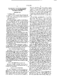
- the single FIGURE is a simplified block diagram of a microcomputer system showing address busses and controls but no data busses.
- the major components of the FIGURE comprise a microprocessor 1 which may be of the type 80286 manufactured by Intel Corp., a bus controller 2 of the type 82288, also produced by Intel Corp., a memory system 3 and a programmable direct memory access (DMA) device which may be of the type 8237A produced by Intel Corp. All of these major components are coupled, through busses, to a number of input/output channel connectors, of which two, referenced 5 and 6, are shown. Each line of a control bus 18, a system address bus 19 and a local address bus 20 is connected to all of the connectors, as are control lines 25 and 26. The remaining busses 27 and 28 each have four lines, each of which is connected to an associated one of the connectors.
- HLDA hold acknowledge
- HRQ hold request
- S0 and S1 bus cycle status signal lines
- Bus controller 2 is responsive to the MIO, S0 and S1 signals to define the type of bus cycle to be performed.
- the defined bus cycle is an I/O read cycle if S1 is low and S0 is high, or an I/O write cycle if S1 is high and S0 is low.
- S1 high and S0 low indicate a memory write cycle
- S1 low and S0 high indicate a memory read cycle.
- bus controller 2 issues a respective command signal, either IOR, IOW, MEMW, or MEMR on a respective one of the lines in command bus 18, with the MEMW and MEMR signals going to memory system 3.
- the last indicated outputs from processor 1 are twenty-four address outputs A0 through A23 which are applied to an address bus 22.
- Lines A0 through A19 of this bus are applied to gate 8 which is enabled, at input E, in the absence of a HLDA signal from processor 1.
- the signals from latch 8 are applied to lines SA0 through SA19 of a system address bus 19, which applies the low order address bits to memory system 3, and I/O devices through connectors 5 and 6.
- Lines A17 through A23 of address bus 22 are coupled to a bi-directional transceiver 9, which is also coupled to lines LA17 through LA23 of a local address bus 20. These provide the high order address bits for the I/O devices on connectors 5 and 6.
- bits A0 through A19 are not latched as are bits A0 through A19, so that the high order bits become available prior to the low order bits, thus allowing preselection of devices by the high order bits prior to address selection within a preselected device.
- Lines A17 through A23 of the address bus 22 are also applied to a memory decoder 10.
- This decoder is a read-only memory which is responsive to the high order address bits to provide enable signals to select either areas within the system random access memory 3, over a bus 30, or the system control read-only memory (not shown).
- the actual address within the selected memory is, of course, defined by the lower order address bits on bus 19 either from latch 8 or from an I/O device on a channel connector.
- a latch 11 is coupled to receive the A16 through A19 bits from bus 22.
- This latch which is enabled from an AND gate 15, is used to direct the A16 through A19 bits to the system address bus 19 during DMA operations.
- a DMA page register and control unit 7 are used to apply bits A16 through A23 to address bus 22 during DMA operations.
- the function of this unit which may be of the byte SN74LS612 produced by Texas Instruments, Inc., is to expand memory addresses during DMA operations.
- this unit includes four 8-bit address registers which can be periodically reloaded from the data bus of processor 1. During DMA operations, these registers can be individually selected by the energization of individual ones of four acknowledge lines in bus 28 applied to inputs MA0 through MA3 of unit 7. Thus, the acknowledge lines, which effect selection of I/O devices for data transfer under DMA control, also provide selection of address bits A16 through A23.
- DMA controller 4 this unit functions to control direct data transfer between memory 3 and I/O units on the I/O connectors including connectors 5 and 6.
- a hold request (HRQ) output is applied to the HOLD input of processor 1 which, as mentioned above, responds to a request signal to enter a hold state and issue a hold acknowledge (HLDA) signal over line 23 to the HLDA input of controller 4.
- HRQ hold request
- HLDA hold acknowledge
- Individual DMA requests from I/O units are applied to controller 4 over a request bus 27 to obtain DMA service. These inputs are prioritized with DRQO having the highest priority and DRQ3 the lowest.
- the DMA acknowledge outputs DACK0 through DACK3 are used to notify individual I/O devices of the grant of a DMA cycle.
- AEN is used to enable addresses during DMA cycles and is applied over a line 29 to a latch 14 and an AND gate 16.
- Data bus input/output terminals D0 through D7 are coupled to the processor 1 data bus (not shown) and through a bus 30 to latch 14.
- the D0 through D7 terminals receive data from processor 1 to update address registers within the controller.
- these registers deliver address bits A8 through A15 through terminals D0 through D7, latch 14 and a bidirectional transceiver 13 to system address bus 19.
- Terminals A0 through A7 operate similarly, but their registers need not be latched externally and deliver address bits A0/A7 through bidirectional transceiver 13 to system address bus 19.
- Control input/output terminals labeled CONTROL, and including I0R, I0W, MEMR and MEMW lines, are coupled to internal control registers in controller 4. During DMA cycles the control data flow is reversed through transceivers 12 to control bus 18.
- The, or each, peripheral processor is arranged to activate this line in response to an acknowledge signal applied over bus 28 to its corresponding channel connector.
- a peripheral processor card is in channel connector 5 and this connector is assigned channel 0.
- Controller 4 responds by issuing a HRQ over line 24 for processor 1 which then enters a hold condition and issues a HDLA output over line 23 to controller 4.
- controller 4 then issues an active high acknowledge signal on the DACK0 line of bus 28 to channel connector 5.
- the peripheral processor includes an inverter coupled between the DACK line and the -MASTER line 25 and, therefore, drops this line to its active (low) state.
- the peripheral processor must now wait for at least one system clock period to allow for system reconfiguration before it starts a bus cycle.
- Line 25 is coupled to AND gate 16, AND gate 15 and to the DIR input of transceiver 9.
- AND gate 16 also receives the address enable (AEN) output of controller 4. AEN goes high with the DACK signal, but the output of AND gate remains high when the -MASTER line goes low. This output, on line 35, controls transceivers 12 and 13 to transmit from right to left, thereby preventing the transmission of data from controller 4 to the system address bus 19 and the control bus 18.
- AND gate 15 receives the HLDA signal on line 23 from processor 1 in addition to the -MASTER signal. With the HLDA high and the -MASTER signal low, the output, on line 36, is high. This will enable latch 11 and disable DMA page register 7.
- An inverter 17 inverts the high signal on line 36 to drop the AEN signal on line 26 to the channel connectors to an inactive state. It will be recalled that the AEN signal, which is normally connected directly from controller to the channel connectors, is used to enable addresses for DMA cycles.
- the -MASTER signal sets transceiver 9 for transmission from right to left.
- the system is now set up for data transfer between the peripheral processor on channel connector 5 and memory 3 or, in fact, any memory or other device coupled to the system except processor 1 and the main control read-only memory.
- the control signals on bus 18 are provided by the peripheral processor.
- Gate 8 and transceiver 13 both now prevent data passing to bus 19 from the processor 1 address outputs at controller 4 address outputs.
- address signals from the peripheral processor on bus 19 are applied to memory 3 and, through latch 11, to bus 22.
- the A16 through A19 signals from this latch are applied through bus 22 to memory decoder 10 to provide suitable enabling signals to select memory 3 over bus 30 if memory 3 is to be selected.
- the local address bits, which as before, are unlatched, are now provided from line 20, through transceiver 9, to decoder 10 over bus 22.
- the peripheral processor can now perform as many bus cycles as it requires as long as it holds its DRQ line to DMA controller 4 on bus 27 active. If, however, memory 3 is a dynamic random access memory, these peripheral bus cycles are limited to allow for memory refresh using either the DMA or a separate refresh system (not shown). After the peripheral processor completes its bus cycles, it tristates its bus drivers to an OFF condition, and drops its DRQ line to the inactive (low) condition. This releases the system back to control from processor 1, controller 4 or another peripheral processor device.
- a logic circuit system looks at the hold acknowledge (HLDA) output of the main processor, a -MASTER input from the peripheral processing device and the address enable (AEN) output of the DMA controller to reconfigure the system address and control busses.
- HLDA hold acknowledge
- AEN address enable
Landscapes
- Engineering & Computer Science (AREA)
- Theoretical Computer Science (AREA)
- Physics & Mathematics (AREA)
- General Engineering & Computer Science (AREA)
- General Physics & Mathematics (AREA)
- Bus Control (AREA)
- Hardware Redundancy (AREA)
- Multi Processors (AREA)
- Exchange Systems With Centralized Control (AREA)
- Microcomputers (AREA)
- Information Transfer Systems (AREA)
- Selective Calling Equipment (AREA)
Priority Applications (14)
| Application Number | Priority Date | Filing Date | Title |
|---|---|---|---|
| US06/589,692 US4528626A (en) | 1984-03-19 | 1984-03-19 | Microcomputer system with bus control means for peripheral processing devices |
| PH31371A PH24588A (en) | 1984-03-19 | 1984-10-26 | Microcomputer system with bus control means for peripheral processing devices |
| KR1019840007514A KR890003323B1 (ko) | 1984-03-19 | 1984-11-29 | 버스 제어수단을 갖춘 마이크로컴퓨터 시스템 |
| JP59252117A JPS60201464A (ja) | 1984-03-19 | 1984-11-30 | マイクロコンピユ−タシステム |
| GB08432313A GB2156113B (en) | 1984-03-19 | 1984-12-20 | Microcomputer data processing systems permitting bus control by peripheral processing devices |
| ZA85183A ZA85183B (en) | 1984-03-19 | 1985-01-08 | Microcomputer system with bus control means for peripheral processing devices |
| DE8585100105T DE3567115D1 (en) | 1984-03-19 | 1985-01-11 | Microocomputer data processing systems permitting bus control by peripheral processing devices |
| AT85100105T ATE39581T1 (de) | 1984-03-19 | 1985-01-11 | Mikrorechner-datenverarbeitungssysteme welche die bussteuerung durch peripherieprozessoren erlaubt. |
| EP85100105A EP0155443B1 (en) | 1984-03-19 | 1985-01-11 | Microocomputer data processing systems permitting bus control by peripheral processing devices |
| CA000473966A CA1221173A (en) | 1984-03-19 | 1985-02-08 | Microcomputer system with bus control means for peripheral processing devices |
| ES540493A ES8606692A1 (es) | 1984-03-19 | 1985-02-18 | Una instalacion de microcomputador en la que el control de linea general puede transferirse del microprocesador princi-pal a dispositivos perifericos |
| BR8500945A BR8500945A (pt) | 1984-03-19 | 1985-03-04 | Arranjo de microcomputador com meio de controle de cabo para dispositivos perifericos de processamento |
| MX204528A MX158688A (es) | 1984-03-19 | 1985-03-07 | Mejoras en sistema de control de microcomputadoras para procesadores perifericos |
| HK423/90A HK42390A (en) | 1984-03-19 | 1990-05-31 | Microcomputer data processing systems permitting bus control by peripheral processing devices |
Applications Claiming Priority (1)
| Application Number | Priority Date | Filing Date | Title |
|---|---|---|---|
| US06/589,692 US4528626A (en) | 1984-03-19 | 1984-03-19 | Microcomputer system with bus control means for peripheral processing devices |
Publications (1)
| Publication Number | Publication Date |
|---|---|
| US4528626A true US4528626A (en) | 1985-07-09 |
Family
ID=24359085
Family Applications (1)
| Application Number | Title | Priority Date | Filing Date |
|---|---|---|---|
| US06/589,692 Expired - Lifetime US4528626A (en) | 1984-03-19 | 1984-03-19 | Microcomputer system with bus control means for peripheral processing devices |
Country Status (14)
| Country | Link |
|---|---|
| US (1) | US4528626A (xx) |
| EP (1) | EP0155443B1 (xx) |
| JP (1) | JPS60201464A (xx) |
| KR (1) | KR890003323B1 (xx) |
| AT (1) | ATE39581T1 (xx) |
| BR (1) | BR8500945A (xx) |
| CA (1) | CA1221173A (xx) |
| DE (1) | DE3567115D1 (xx) |
| ES (1) | ES8606692A1 (xx) |
| GB (1) | GB2156113B (xx) |
| HK (1) | HK42390A (xx) |
| MX (1) | MX158688A (xx) |
| PH (1) | PH24588A (xx) |
| ZA (1) | ZA85183B (xx) |
Cited By (24)
| Publication number | Priority date | Publication date | Assignee | Title |
|---|---|---|---|---|
| US4594654A (en) * | 1983-11-04 | 1986-06-10 | Advanced Micro Devices, Inc. | Circuit for controlling external bipolar buffers from an MOS peripheral device |
| US4794523A (en) * | 1985-09-30 | 1988-12-27 | Manolito Adan | Cache memory architecture for microcomputer speed-up board |
| US4807112A (en) * | 1984-10-11 | 1989-02-21 | Nec Corporation | Microcomputer with a bus accessible from an external apparatus |
| EP0317466A2 (en) * | 1987-11-18 | 1989-05-24 | International Business Machines Corporation | Reverse flow control mechanism and method |
| US4901234A (en) * | 1987-03-27 | 1990-02-13 | International Business Machines Corporation | Computer system having programmable DMA control |
| US4918597A (en) * | 1984-12-14 | 1990-04-17 | Alcatel Usa Corp. | Adaptive interface for transferring segmented message between device and microcomputer on line division multiplexed bus |
| US4975832A (en) * | 1987-06-25 | 1990-12-04 | Teac Corporation | Microcomputer system with dual DMA mode transmissions |
| US4987529A (en) * | 1988-08-11 | 1991-01-22 | Ast Research, Inc. | Shared memory bus system for arbitrating access control among contending memory refresh circuits, peripheral controllers, and bus masters |
| US4989113A (en) * | 1987-03-13 | 1991-01-29 | Texas Instruments Incorporated | Data processing device having direct memory access with improved transfer control |
| US5003463A (en) * | 1988-06-30 | 1991-03-26 | Wang Laboratories, Inc. | Interface controller with first and second buffer storage area for receiving and transmitting data between I/O bus and high speed system bus |
| DE4031661A1 (de) * | 1989-10-05 | 1991-04-18 | Mitsubishi Electric Corp | System zum ueberwachen direkten speicherzugriffs |
| US5099417A (en) * | 1987-03-13 | 1992-03-24 | Texas Instruments Incorporated | Data processing device with improved direct memory access |
| US5191657A (en) * | 1989-11-09 | 1993-03-02 | Ast Research, Inc. | Microcomputer architecture utilizing an asynchronous bus between microprocessor and industry standard synchronous bus |
| US5261057A (en) * | 1988-06-30 | 1993-11-09 | Wang Laboratories, Inc. | I/O bus to system interface |
| US5392405A (en) * | 1987-10-20 | 1995-02-21 | Sharp Kabushiki Kaisha | Data processor for detecting identical data coexisting in a plurality of data sections of data transmission paths |
| US5412783A (en) * | 1991-11-10 | 1995-05-02 | Hewlett-Packard Company | Method for efficient serialized transmission of handshake signal on a digital bus |
| US5546563A (en) * | 1991-04-22 | 1996-08-13 | Acer Incorporated | Single chip replacement upgradeable computer motherboard with enablement of inserted upgrade CPU chip |
| US5577214A (en) * | 1992-05-18 | 1996-11-19 | Opti, Inc. | Programmable hold delay |
| US5590375A (en) * | 1992-08-10 | 1996-12-31 | Advanced Logic Research | Apparatus for performing concurrent seeks on plural integrated drive electronics (IDE) disk drives without additional devices |
| US5619729A (en) * | 1993-12-02 | 1997-04-08 | Intel Corporation | Power management of DMA slaves with DMA traps |
| US5761479A (en) * | 1991-04-22 | 1998-06-02 | Acer Incorporated | Upgradeable/downgradeable central processing unit chip computer systems |
| US5978866A (en) * | 1997-03-10 | 1999-11-02 | Integrated Technology Express, Inc. | Distributed pre-fetch buffer for multiple DMA channel device |
| US6460095B1 (en) * | 1998-12-18 | 2002-10-01 | Matsushita Electric Industrial Co., Ltd. | Data transfer apparatus, data transfer system and recording medium |
| US7036064B1 (en) * | 2000-11-13 | 2006-04-25 | Omar Kebichi | Synchronization point across different memory BIST controllers |
Families Citing this family (1)
| Publication number | Priority date | Publication date | Assignee | Title |
|---|---|---|---|---|
| US4847750A (en) * | 1986-02-13 | 1989-07-11 | Intelligent Instrumentation, Inc. | Peripheral DMA controller for data acquisition system |
Citations (3)
| Publication number | Priority date | Publication date | Assignee | Title |
|---|---|---|---|---|
| US4047158A (en) * | 1974-12-13 | 1977-09-06 | Pertec Corporation | Peripheral processing system |
| US4112490A (en) * | 1976-11-24 | 1978-09-05 | Intel Corporation | Data transfer control apparatus and method |
| US4180855A (en) * | 1978-04-07 | 1979-12-25 | Gte Automatic Electric Laboratories Incorporated | Direct memory access expander unit for use with a microprocessor |
Family Cites Families (3)
| Publication number | Priority date | Publication date | Assignee | Title |
|---|---|---|---|---|
| GB1485758A (en) * | 1973-09-16 | 1977-09-14 | Hawker Siddeley Dynamics Ltd | Computer systems |
| DE2824557C2 (de) * | 1978-06-05 | 1983-01-20 | Siemens AG, 1000 Berlin und 8000 München | Anordnung in Mikroprozessoren für den Aufbau von Multiprozessor-Systemen |
| EP0057756B1 (de) * | 1981-02-11 | 1985-02-20 | Siemens Aktiengesellschaft | Anordnung zum Datenaustausch in parallel arbeitenden Multi-Mikrorechnersystemen |
-
1984
- 1984-03-19 US US06/589,692 patent/US4528626A/en not_active Expired - Lifetime
- 1984-10-26 PH PH31371A patent/PH24588A/en unknown
- 1984-11-29 KR KR1019840007514A patent/KR890003323B1/ko not_active IP Right Cessation
- 1984-11-30 JP JP59252117A patent/JPS60201464A/ja active Granted
- 1984-12-20 GB GB08432313A patent/GB2156113B/en not_active Expired
-
1985
- 1985-01-08 ZA ZA85183A patent/ZA85183B/xx unknown
- 1985-01-11 EP EP85100105A patent/EP0155443B1/en not_active Expired
- 1985-01-11 DE DE8585100105T patent/DE3567115D1/de not_active Expired
- 1985-01-11 AT AT85100105T patent/ATE39581T1/de not_active IP Right Cessation
- 1985-02-08 CA CA000473966A patent/CA1221173A/en not_active Expired
- 1985-02-18 ES ES540493A patent/ES8606692A1/es not_active Expired
- 1985-03-04 BR BR8500945A patent/BR8500945A/pt not_active IP Right Cessation
- 1985-03-07 MX MX204528A patent/MX158688A/es unknown
-
1990
- 1990-05-31 HK HK423/90A patent/HK42390A/xx not_active IP Right Cessation
Patent Citations (3)
| Publication number | Priority date | Publication date | Assignee | Title |
|---|---|---|---|---|
| US4047158A (en) * | 1974-12-13 | 1977-09-06 | Pertec Corporation | Peripheral processing system |
| US4112490A (en) * | 1976-11-24 | 1978-09-05 | Intel Corporation | Data transfer control apparatus and method |
| US4180855A (en) * | 1978-04-07 | 1979-12-25 | Gte Automatic Electric Laboratories Incorporated | Direct memory access expander unit for use with a microprocessor |
Non-Patent Citations (2)
| Title |
|---|
| Computer I/O Part V Kolobaud Classroom, published by Peter Stale in Microcomputing, Mar. 1979, pp. 108 112. * |
| Computer I/O Part V Kolobaud Classroom, published by Peter Stale in Microcomputing, Mar. 1979, pp. 108-112. |
Cited By (31)
| Publication number | Priority date | Publication date | Assignee | Title |
|---|---|---|---|---|
| US4594654A (en) * | 1983-11-04 | 1986-06-10 | Advanced Micro Devices, Inc. | Circuit for controlling external bipolar buffers from an MOS peripheral device |
| US4807112A (en) * | 1984-10-11 | 1989-02-21 | Nec Corporation | Microcomputer with a bus accessible from an external apparatus |
| US4918597A (en) * | 1984-12-14 | 1990-04-17 | Alcatel Usa Corp. | Adaptive interface for transferring segmented message between device and microcomputer on line division multiplexed bus |
| US4794523A (en) * | 1985-09-30 | 1988-12-27 | Manolito Adan | Cache memory architecture for microcomputer speed-up board |
| US4989113A (en) * | 1987-03-13 | 1991-01-29 | Texas Instruments Incorporated | Data processing device having direct memory access with improved transfer control |
| US5099417A (en) * | 1987-03-13 | 1992-03-24 | Texas Instruments Incorporated | Data processing device with improved direct memory access |
| US4901234A (en) * | 1987-03-27 | 1990-02-13 | International Business Machines Corporation | Computer system having programmable DMA control |
| US4975832A (en) * | 1987-06-25 | 1990-12-04 | Teac Corporation | Microcomputer system with dual DMA mode transmissions |
| US5392405A (en) * | 1987-10-20 | 1995-02-21 | Sharp Kabushiki Kaisha | Data processor for detecting identical data coexisting in a plurality of data sections of data transmission paths |
| EP0317466A2 (en) * | 1987-11-18 | 1989-05-24 | International Business Machines Corporation | Reverse flow control mechanism and method |
| EP0317466A3 (en) * | 1987-11-18 | 1991-01-30 | International Business Machines Corporation | Reverse flow control mechanism and method |
| US4930069A (en) * | 1987-11-18 | 1990-05-29 | International Business Machines Corporation | Mechanism and method for transferring data between bus units having varying master and slave DMA capabilities |
| US5003463A (en) * | 1988-06-30 | 1991-03-26 | Wang Laboratories, Inc. | Interface controller with first and second buffer storage area for receiving and transmitting data between I/O bus and high speed system bus |
| US5261057A (en) * | 1988-06-30 | 1993-11-09 | Wang Laboratories, Inc. | I/O bus to system interface |
| US4987529A (en) * | 1988-08-11 | 1991-01-22 | Ast Research, Inc. | Shared memory bus system for arbitrating access control among contending memory refresh circuits, peripheral controllers, and bus masters |
| US5438666A (en) * | 1988-08-11 | 1995-08-01 | Ast Research, Inc. | Shared memory bus system for arbitrating access control among contending memory refresh circuits, peripheral controllers, and bus masters |
| DE4031661A1 (de) * | 1989-10-05 | 1991-04-18 | Mitsubishi Electric Corp | System zum ueberwachen direkten speicherzugriffs |
| US5539916A (en) * | 1989-10-05 | 1996-07-23 | Mitsubishi Denki Kabushiki Kaisha | DMA control for continuing transfer to input/output device in a cycle steal mode |
| US5191657A (en) * | 1989-11-09 | 1993-03-02 | Ast Research, Inc. | Microcomputer architecture utilizing an asynchronous bus between microprocessor and industry standard synchronous bus |
| US5555381A (en) * | 1989-11-09 | 1996-09-10 | Ast Research, Inc. | Microcomputer architecture utilizing an asynchronous bus between microprocessor and industry standard synchronous bus |
| US5546563A (en) * | 1991-04-22 | 1996-08-13 | Acer Incorporated | Single chip replacement upgradeable computer motherboard with enablement of inserted upgrade CPU chip |
| US5761479A (en) * | 1991-04-22 | 1998-06-02 | Acer Incorporated | Upgradeable/downgradeable central processing unit chip computer systems |
| US5412783A (en) * | 1991-11-10 | 1995-05-02 | Hewlett-Packard Company | Method for efficient serialized transmission of handshake signal on a digital bus |
| US5577214A (en) * | 1992-05-18 | 1996-11-19 | Opti, Inc. | Programmable hold delay |
| US5590375A (en) * | 1992-08-10 | 1996-12-31 | Advanced Logic Research | Apparatus for performing concurrent seeks on plural integrated drive electronics (IDE) disk drives without additional devices |
| US5708848A (en) * | 1992-08-10 | 1998-01-13 | Advanced Logic Research, Inc. | Paddle board interface for concurrent seeks on multiple disk drives of a computer |
| US5778252A (en) * | 1992-08-10 | 1998-07-07 | Advanced Research Logic, Inc. | On-board interface for concurrent seeks of multiple disk drives of a computer |
| US5619729A (en) * | 1993-12-02 | 1997-04-08 | Intel Corporation | Power management of DMA slaves with DMA traps |
| US5978866A (en) * | 1997-03-10 | 1999-11-02 | Integrated Technology Express, Inc. | Distributed pre-fetch buffer for multiple DMA channel device |
| US6460095B1 (en) * | 1998-12-18 | 2002-10-01 | Matsushita Electric Industrial Co., Ltd. | Data transfer apparatus, data transfer system and recording medium |
| US7036064B1 (en) * | 2000-11-13 | 2006-04-25 | Omar Kebichi | Synchronization point across different memory BIST controllers |
Also Published As
| Publication number | Publication date |
|---|---|
| ES540493A0 (es) | 1986-04-01 |
| GB8432313D0 (en) | 1985-01-30 |
| ZA85183B (en) | 1985-11-27 |
| PH24588A (en) | 1990-08-17 |
| EP0155443A1 (en) | 1985-09-25 |
| JPS60201464A (ja) | 1985-10-11 |
| DE3567115D1 (en) | 1989-02-02 |
| ATE39581T1 (de) | 1989-01-15 |
| GB2156113B (en) | 1987-03-25 |
| KR890003323B1 (ko) | 1989-09-16 |
| MX158688A (es) | 1989-02-27 |
| HK42390A (en) | 1990-06-08 |
| GB2156113A (en) | 1985-10-02 |
| JPH0228181B2 (xx) | 1990-06-21 |
| EP0155443B1 (en) | 1988-12-28 |
| KR850007129A (ko) | 1985-10-30 |
| BR8500945A (pt) | 1985-10-22 |
| ES8606692A1 (es) | 1986-04-01 |
| CA1221173A (en) | 1987-04-28 |
Similar Documents
| Publication | Publication Date | Title |
|---|---|---|
| US4528626A (en) | Microcomputer system with bus control means for peripheral processing devices | |
| US5555425A (en) | Multi-master bus arbitration system in which the address and data lines of the bus may be separately granted to individual masters | |
| KR970000842B1 (ko) | 정보 처리 시스템 및 컴퓨터 시스템 | |
| US5125093A (en) | Interrupt control for multiprocessor computer system | |
| US4935868A (en) | Multiple port bus interface controller with slave bus | |
| JP2552085B2 (ja) | マルチプル・バスの調停論理のためのシステム及び方法 | |
| US4817037A (en) | Data processing system with overlap bus cycle operations | |
| US5101497A (en) | Programmable interrupt controller | |
| EP1163593B1 (en) | Apparatus for communicating between multiple functional units in a computer environment | |
| EP0081961A2 (en) | Synchronous data bus system with automatically variable data rate | |
| US5420985A (en) | Bus arbiter system and method utilizing hardware and software which is capable of operation in distributed mode or central mode | |
| US5925118A (en) | Methods and architectures for overlapped read and write operations | |
| JPS5837585B2 (ja) | ケイサンキソウチ | |
| JPH056223B2 (xx) | ||
| US5566345A (en) | SCSI bus capacity expansion controller using gating circuits to arbitrate DMA requests from a plurality of disk drives | |
| US6959354B2 (en) | Effective bus utilization using multiple bus interface circuits and arbitration logic circuit | |
| US4300194A (en) | Data processing system having multiple common buses | |
| US5664142A (en) | Chained DMA devices for crossing common buses | |
| US5862375A (en) | System for effecting communications between a computing device and a plurality of peripheral devices | |
| JPS6119062B2 (xx) | ||
| US5341508A (en) | Processing unit having multiple synchronous bus for sharing access and regulating system bus access to synchronous bus | |
| GB2119977A (en) | Microcomputer systems | |
| JPH0227696B2 (ja) | Johoshorisochi | |
| US7206878B2 (en) | Voltage level bus protocol for transferring data | |
| JPS6337418B2 (xx) |
Legal Events
| Date | Code | Title | Description |
|---|---|---|---|
| AS | Assignment |
Owner name: INTERNATIONAL BUSINESS MACHINES CORPORATION, ARMON Free format text: ASSIGNMENT OF ASSIGNORS INTEREST.;ASSIGNORS:DEAN, MARK E.;MOELLER, DENNIS L.;REEL/FRAME:004239/0783;SIGNING DATES FROM 19840314 TO 19840315 |
|
| STCF | Information on status: patent grant |
Free format text: PATENTED CASE |
|
| FPAY | Fee payment |
Year of fee payment: 4 |
|
| CC | Certificate of correction | ||
| FPAY | Fee payment |
Year of fee payment: 8 |
|
| FPAY | Fee payment |
Year of fee payment: 12 |