US3778899A - Mounting preformed circuits on flexible dielectric substrates - Google Patents
Mounting preformed circuits on flexible dielectric substrates Download PDFInfo
- Publication number
- US3778899A US3778899A US00198147A US3778899DA US3778899A US 3778899 A US3778899 A US 3778899A US 00198147 A US00198147 A US 00198147A US 3778899D A US3778899D A US 3778899DA US 3778899 A US3778899 A US 3778899A
- Authority
- US
- United States
- Prior art keywords
- circuit
- preformed
- circuits
- flexible dielectric
- dielectric substrate
- Prior art date
- Legal status (The legal status is an assumption and is not a legal conclusion. Google has not performed a legal analysis and makes no representation as to the accuracy of the status listed.)
- Expired - Lifetime
Links
- 239000000758 substrate Substances 0.000 title abstract description 34
- 238000000034 method Methods 0.000 claims description 17
- ROOXNKNUYICQNP-UHFFFAOYSA-N ammonium persulfate Chemical compound [NH4+].[NH4+].[O-]S(=O)(=O)OOS([O-])(=O)=O ROOXNKNUYICQNP-UHFFFAOYSA-N 0.000 claims description 12
- 239000005708 Sodium hypochlorite Substances 0.000 claims description 7
- 239000000463 material Substances 0.000 claims description 7
- SUKJFIGYRHOWBL-UHFFFAOYSA-N sodium hypochlorite Chemical compound [Na+].Cl[O-] SUKJFIGYRHOWBL-UHFFFAOYSA-N 0.000 claims description 7
- 229910001870 ammonium persulfate Inorganic materials 0.000 claims description 6
- 238000005406 washing Methods 0.000 claims description 5
- 238000001035 drying Methods 0.000 claims description 3
- 125000004430 oxygen atom Chemical group O* 0.000 abstract description 13
- 239000001257 hydrogen Substances 0.000 abstract description 7
- 229910052739 hydrogen Inorganic materials 0.000 abstract description 7
- 238000004519 manufacturing process Methods 0.000 abstract description 2
- 239000010410 layer Substances 0.000 description 9
- 239000002356 single layer Substances 0.000 description 8
- 239000011888 foil Substances 0.000 description 6
- RYGMFSIKBFXOCR-UHFFFAOYSA-N Copper Chemical compound [Cu] RYGMFSIKBFXOCR-UHFFFAOYSA-N 0.000 description 5
- 239000000126 substance Substances 0.000 description 5
- QVGXLLKOCUKJST-UHFFFAOYSA-N atomic oxygen Chemical compound [O] QVGXLLKOCUKJST-UHFFFAOYSA-N 0.000 description 4
- 229910052802 copper Inorganic materials 0.000 description 4
- 239000010949 copper Substances 0.000 description 4
- 125000004435 hydrogen atom Chemical group [H]* 0.000 description 4
- 239000001301 oxygen Substances 0.000 description 4
- 229910052760 oxygen Inorganic materials 0.000 description 4
- 239000011347 resin Substances 0.000 description 4
- 229920005989 resin Polymers 0.000 description 4
- 239000000243 solution Substances 0.000 description 4
- 238000003475 lamination Methods 0.000 description 3
- 238000007254 oxidation reaction Methods 0.000 description 3
- PXHVJJICTQNCMI-UHFFFAOYSA-N Nickel Chemical compound [Ni] PXHVJJICTQNCMI-UHFFFAOYSA-N 0.000 description 2
- 239000002184 metal Substances 0.000 description 2
- 229910052751 metal Inorganic materials 0.000 description 2
- 239000000203 mixture Substances 0.000 description 2
- 229920001169 thermoplastic Polymers 0.000 description 2
- 239000004416 thermosoftening plastic Substances 0.000 description 2
- 241000380131 Ammophila arenaria Species 0.000 description 1
- XEEYBQQBJWHFJM-UHFFFAOYSA-N Iron Chemical compound [Fe] XEEYBQQBJWHFJM-UHFFFAOYSA-N 0.000 description 1
- 239000004698 Polyethylene Substances 0.000 description 1
- 239000000853 adhesive Substances 0.000 description 1
- 230000001070 adhesive effect Effects 0.000 description 1
- 239000012670 alkaline solution Substances 0.000 description 1
- 238000009835 boiling Methods 0.000 description 1
- 238000006664 bond formation reaction Methods 0.000 description 1
- 239000011248 coating agent Substances 0.000 description 1
- 238000000576 coating method Methods 0.000 description 1
- 239000011889 copper foil Substances 0.000 description 1
- 238000010030 laminating Methods 0.000 description 1
- 150000002739 metals Chemical class 0.000 description 1
- 229910052759 nickel Inorganic materials 0.000 description 1
- 230000001590 oxidative effect Effects 0.000 description 1
- 239000004033 plastic Substances 0.000 description 1
- 229920003023 plastic Polymers 0.000 description 1
- -1 polyethylene Polymers 0.000 description 1
- 229920000573 polyethylene Polymers 0.000 description 1
- 238000006748 scratching Methods 0.000 description 1
- 230000002393 scratching effect Effects 0.000 description 1
- 229910001220 stainless steel Inorganic materials 0.000 description 1
- 239000010935 stainless steel Substances 0.000 description 1
- XLYOFNOQVPJJNP-UHFFFAOYSA-N water Substances O XLYOFNOQVPJJNP-UHFFFAOYSA-N 0.000 description 1
Images
Classifications
-
- B—PERFORMING OPERATIONS; TRANSPORTING
- B32—LAYERED PRODUCTS
- B32B—LAYERED PRODUCTS, i.e. PRODUCTS BUILT-UP OF STRATA OF FLAT OR NON-FLAT, e.g. CELLULAR OR HONEYCOMB, FORM
- B32B7/00—Layered products characterised by the relation between layers; Layered products characterised by the relative orientation of features between layers, or by the relative values of a measurable parameter between layers, i.e. products comprising layers having different physical, chemical or physicochemical properties; Layered products characterised by the interconnection of layers
- B32B7/04—Interconnection of layers
- B32B7/05—Interconnection of layers the layers not being connected over the whole surface, e.g. discontinuous connection or patterned connection
-
- H—ELECTRICITY
- H05—ELECTRIC TECHNIQUES NOT OTHERWISE PROVIDED FOR
- H05K—PRINTED CIRCUITS; CASINGS OR CONSTRUCTIONAL DETAILS OF ELECTRIC APPARATUS; MANUFACTURE OF ASSEMBLAGES OF ELECTRICAL COMPONENTS
- H05K3/00—Apparatus or processes for manufacturing printed circuits
- H05K3/10—Apparatus or processes for manufacturing printed circuits in which conductive material is applied to the insulating support in such a manner as to form the desired conductive pattern
- H05K3/20—Apparatus or processes for manufacturing printed circuits in which conductive material is applied to the insulating support in such a manner as to form the desired conductive pattern by affixing prefabricated conductor pattern
- H05K3/205—Apparatus or processes for manufacturing printed circuits in which conductive material is applied to the insulating support in such a manner as to form the desired conductive pattern by affixing prefabricated conductor pattern using a pattern electroplated or electroformed on a metallic carrier
-
- B—PERFORMING OPERATIONS; TRANSPORTING
- B32—LAYERED PRODUCTS
- B32B—LAYERED PRODUCTS, i.e. PRODUCTS BUILT-UP OF STRATA OF FLAT OR NON-FLAT, e.g. CELLULAR OR HONEYCOMB, FORM
- B32B15/00—Layered products comprising a layer of metal
- B32B15/20—Layered products comprising a layer of metal comprising aluminium or copper
-
- H—ELECTRICITY
- H05—ELECTRIC TECHNIQUES NOT OTHERWISE PROVIDED FOR
- H05K—PRINTED CIRCUITS; CASINGS OR CONSTRUCTIONAL DETAILS OF ELECTRIC APPARATUS; MANUFACTURE OF ASSEMBLAGES OF ELECTRICAL COMPONENTS
- H05K3/00—Apparatus or processes for manufacturing printed circuits
- H05K3/38—Improvement of the adhesion between the insulating substrate and the metal
- H05K3/382—Improvement of the adhesion between the insulating substrate and the metal by special treatment of the metal
- H05K3/385—Improvement of the adhesion between the insulating substrate and the metal by special treatment of the metal by conversion of the surface of the metal, e.g. by oxidation, whether or not followed by reaction or removal of the converted layer
-
- B—PERFORMING OPERATIONS; TRANSPORTING
- B32—LAYERED PRODUCTS
- B32B—LAYERED PRODUCTS, i.e. PRODUCTS BUILT-UP OF STRATA OF FLAT OR NON-FLAT, e.g. CELLULAR OR HONEYCOMB, FORM
- B32B2457/00—Electrical equipment
-
- H—ELECTRICITY
- H05—ELECTRIC TECHNIQUES NOT OTHERWISE PROVIDED FOR
- H05K—PRINTED CIRCUITS; CASINGS OR CONSTRUCTIONAL DETAILS OF ELECTRIC APPARATUS; MANUFACTURE OF ASSEMBLAGES OF ELECTRICAL COMPONENTS
- H05K1/00—Printed circuits
- H05K1/02—Details
- H05K1/03—Use of materials for the substrate
- H05K1/0393—Flexible materials
-
- H—ELECTRICITY
- H05—ELECTRIC TECHNIQUES NOT OTHERWISE PROVIDED FOR
- H05K—PRINTED CIRCUITS; CASINGS OR CONSTRUCTIONAL DETAILS OF ELECTRIC APPARATUS; MANUFACTURE OF ASSEMBLAGES OF ELECTRICAL COMPONENTS
- H05K2203/00—Indexing scheme relating to apparatus or processes for manufacturing printed circuits covered by H05K3/00
- H05K2203/01—Tools for processing; Objects used during processing
- H05K2203/0147—Carriers and holders
- H05K2203/0152—Temporary metallic carrier, e.g. for transferring material
-
- H—ELECTRICITY
- H05—ELECTRIC TECHNIQUES NOT OTHERWISE PROVIDED FOR
- H05K—PRINTED CIRCUITS; CASINGS OR CONSTRUCTIONAL DETAILS OF ELECTRIC APPARATUS; MANUFACTURE OF ASSEMBLAGES OF ELECTRICAL COMPONENTS
- H05K2203/00—Indexing scheme relating to apparatus or processes for manufacturing printed circuits covered by H05K3/00
- H05K2203/03—Metal processing
- H05K2203/0315—Oxidising metal
-
- H—ELECTRICITY
- H05—ELECTRIC TECHNIQUES NOT OTHERWISE PROVIDED FOR
- H05K—PRINTED CIRCUITS; CASINGS OR CONSTRUCTIONAL DETAILS OF ELECTRIC APPARATUS; MANUFACTURE OF ASSEMBLAGES OF ELECTRICAL COMPONENTS
- H05K2203/00—Indexing scheme relating to apparatus or processes for manufacturing printed circuits covered by H05K3/00
- H05K2203/07—Treatments involving liquids, e.g. plating, rinsing
- H05K2203/0703—Plating
- H05K2203/0726—Electroforming, i.e. electroplating on a metallic carrier thereby forming a self-supporting structure
-
- Y—GENERAL TAGGING OF NEW TECHNOLOGICAL DEVELOPMENTS; GENERAL TAGGING OF CROSS-SECTIONAL TECHNOLOGIES SPANNING OVER SEVERAL SECTIONS OF THE IPC; TECHNICAL SUBJECTS COVERED BY FORMER USPC CROSS-REFERENCE ART COLLECTIONS [XRACs] AND DIGESTS
- Y10—TECHNICAL SUBJECTS COVERED BY FORMER USPC
- Y10T—TECHNICAL SUBJECTS COVERED BY FORMER US CLASSIFICATION
- Y10T29/00—Metal working
- Y10T29/49—Method of mechanical manufacture
- Y10T29/49002—Electrical device making
- Y10T29/49117—Conductor or circuit manufacturing
- Y10T29/49124—On flat or curved insulated base, e.g., printed circuit, etc.
- Y10T29/49128—Assembling formed circuit to base
-
- Y—GENERAL TAGGING OF NEW TECHNOLOGICAL DEVELOPMENTS; GENERAL TAGGING OF CROSS-SECTIONAL TECHNOLOGIES SPANNING OVER SEVERAL SECTIONS OF THE IPC; TECHNICAL SUBJECTS COVERED BY FORMER USPC CROSS-REFERENCE ART COLLECTIONS [XRACs] AND DIGESTS
- Y10—TECHNICAL SUBJECTS COVERED BY FORMER USPC
- Y10T—TECHNICAL SUBJECTS COVERED BY FORMER US CLASSIFICATION
- Y10T29/00—Metal working
- Y10T29/49—Method of mechanical manufacture
- Y10T29/49002—Electrical device making
- Y10T29/49117—Conductor or circuit manufacturing
- Y10T29/49124—On flat or curved insulated base, e.g., printed circuit, etc.
- Y10T29/49155—Manufacturing circuit on or in base
Definitions
- ABSTRACT A process for preparing preformed circuits for mounting on a flexible dielectric substrate in which the preformed circuit is subject to a strong alkaline bath so as to add oxygen atoms to the surface of the circuit to increase the incidence of hydrogen bonds between the circuits and the dielectric substrate.
- flexible printed circuitry has generally been constructed by laminating a metallic foil, such as copper, to a flexible dielectric substrate.
- the substrate may comprise a dielectric film with a suitable adhesive on it designed to hold the metallic foil in place.
- Other variations include thermoplastics such as polyethylene in which the metallic foil is affixed to the surface thereof through the application of heat.
- a new type of flexible dielectric substrate comprises a resin base which is bonded to the copper foil during the curing of the substrate itself.
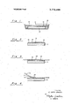
- FIGS. 1, 2, 3 and 4 show subsequent major steps in the process of bonding a preformed circuit to a dielectric substrate according to the present invention.
- a suitable base plate is shown having some type of preformed circuit 12 electrodeposited or otherwise formed on the top surface.
- Base 10 may comprise stainlesssteel, nickel, or any other suitable base material and may or may not include a resist coating 14 in the areas not covered by the preformed circuit 12.
- a resist 14 is used in the uncovered areas and therefore, this structure is shown in 'FIG. 1.
- the preformed circuit 12 comprises copper although other conducting metals may be employed as well. It should be noted that in the prior art preformed circuit 12 would simply be bonded to a dielectric substrate in order to form a printed circuit. Such bonds have been found to be undesirable weak in many cases.
- the present invention adds several additional steps designed to provide a much more secure and tenacious bond between the preformed circuit l2 and the dielectric substrate 22. This is particularly advantageous with flexible dielectric circuits in which the bond between the substrate and the circuit is subject to considerable stress.
- base plate 10 and preformed circuit 12 are immersed in a suitable bath 18 which comprises a strong alkaline solution containing labile oxygen to slightly oxidize the surface of the copper preformed circuit 12.
- a strong alkaline solution containing labile oxygen to slightly oxidize the surface of the copper preformed circuit 12.
- sodium hypochlorite or ammonium persulfate have been used with considerable success although other strong oxidizers may also be suitable.
- oxygen atoms it is essential that a very thin layer of oxygen atoms be established on the surface of the preformed circuit, preferably approximating the thickness of a single layer of oxygen atoms.
- This layer of oxygen atoms is referred to as a mono-layer herein.
- these oxygen atoms are believed to have the capability of forming weak chemical bonds or hydrogen bonds with the hydrogen atoms found in the dielectric substrate materials typically used.
- Substrate materials include most thermoplastics and resin based plastics, all of which have an abundance of hydrogen atoms in their chemical composition. The bath treatment must not be extended too long or conducted at too high a temperature since the oxidization can proceed to the point where more than a monolayer is developed.
- a thick layer of oxidization material actually produces a weaker bond than what would otherwise be the case, and this is, therefore, undesirable.
- the bath treatment should be conducted at temperatures in the range of about 85 to 95C. It was also found that the bath should last at least 10 seconds but should not last longer than about 200 seconds. The most successful bonds were created at a temperature of about 90C. and for periods of time close to 30 seconds. With these temperatures and times, mono-layers of oxygen were consistently developed on the surface of the copper preformed circuit. The process can be conducted at higher temperatures for shorter times but this has been found to be undesirable due to the fact that the higher temperatures generally initiate boiling in the solutions which has been found to degrade their performance.
- the ammonium persulfate solution differs from the sodium hypochlorite solution in that temperatures in the range of to C. are more suitable.
- base 10 is removed from the bath with a very thin mono-layer 20 comprising oxygen atoms suitable for forming hydrogen bonds.
- the base is rinsed with water to remove any remaining solution from the bath and hot air dried to avoid any possible scratching of the surface which would remove the delicate mono-layer of oxygen atoms and thereby de-- grade the bond at the scratch.
- the preformed circuit may be bonded to the dielectric substrate 22 as shown in FIG. 3.
- Substrate 22 is applied directly to the preformed circuit 12 under pressure and heat so as to laminate the dielectric substrate to the preformed circuit and induce the hydrogen bond formations.
- the preferred embodiment uses a resin base dielectric substrate as described in the above-referenced co-pending application. In this process the resin based substrate is partially cured before lamination and then finally cured during lamination.
- the final curing and lamination takes place at a temperature in the range of about 300+ F. to 500 F. and under a pressure of from 50 pounds to 750 pounds per square inch.
- the dielectric substrate 22 is stripped from the base as shown in FIG. 4.
- Preformed circuit 12 remains tenaciously bonded to the substrate due to the hydrogen bonds formed at the junction between circuit 12 and substrate 22.
- a process for bonding preformed circuits to flexible dielectric substrates comprising the steps of forming the circuit on a base, immersing the base and circuit in an oxidizing alkaline bath for a period of time in the range of l0 to 200 seconds to form a very thin monolayer of 'oxide approximately the thickness of a single layer of oxygen atoms on the surface of the circuit, rinsing and drying the circuit, bonding a flexible dielectric to the oxidized face of the preformed circuit, and stripping the substrate with the circuit bonded thereto from the base.
- said alkaline bath comprises sodium hypochlorite at a temperature in the range of 85 to 95 C.
Landscapes
- Engineering & Computer Science (AREA)
- Manufacturing & Machinery (AREA)
- Microelectronics & Electronic Packaging (AREA)
- Chemical & Material Sciences (AREA)
- Chemical Kinetics & Catalysis (AREA)
- Manufacturing Of Printed Wiring (AREA)
- Laminated Bodies (AREA)
Applications Claiming Priority (1)
| Application Number | Priority Date | Filing Date | Title |
|---|---|---|---|
| US19814771A | 1971-11-12 | 1971-11-12 |
Publications (1)
| Publication Number | Publication Date |
|---|---|
| US3778899A true US3778899A (en) | 1973-12-18 |
Family
ID=22732180
Family Applications (1)
| Application Number | Title | Priority Date | Filing Date |
|---|---|---|---|
| US00198147A Expired - Lifetime US3778899A (en) | 1971-11-12 | 1971-11-12 | Mounting preformed circuits on flexible dielectric substrates |
Country Status (9)
| Country | Link |
|---|---|
| US (1) | US3778899A (fa) |
| JP (1) | JPS5547476B2 (fa) |
| BE (1) | BE787386A (fa) |
| CA (1) | CA980463A (fa) |
| DE (1) | DE2240853A1 (fa) |
| FR (1) | FR2159286A1 (fa) |
| GB (1) | GB1392125A (fa) |
| IT (1) | IT969963B (fa) |
| NL (1) | NL7215259A (fa) |
Cited By (13)
| Publication number | Priority date | Publication date | Assignee | Title |
|---|---|---|---|---|
| US3838506A (en) * | 1973-04-09 | 1974-10-01 | Ibm | Aluminum surface and treatment thereof to enhance adhesion in printed circuit laminates |
| US3960561A (en) * | 1975-04-10 | 1976-06-01 | International Business Machines Corporation | Method for making electrical lead frame devices |
| FR2408276A1 (fr) * | 1977-11-07 | 1979-06-01 | Ibm | Procede de traitement de substrats revetus de circuits obtenus par placage additif en vue d'ameliorer l'adherence des circuits |
| US4627162A (en) * | 1983-11-04 | 1986-12-09 | Augat Incorporated | Method of producing a wired circuit board |
| US4648180A (en) * | 1983-11-04 | 1987-03-10 | Augat Inc. | Method of producing a wired circuit board |
| US4698275A (en) * | 1983-11-04 | 1987-10-06 | Augat Inc. | Wire mat mateable with a circuit board |
| US5250758A (en) * | 1991-05-21 | 1993-10-05 | Elf Technologies, Inc. | Methods and systems of preparing extended length flexible harnesses |
| US5354205A (en) * | 1991-08-26 | 1994-10-11 | Hughes Aircraft Company | Electrical connections with shaped contacts |
| US5826329A (en) * | 1995-12-19 | 1998-10-27 | Ncr Corporation | Method of making printed circuit board using thermal transfer techniques |
| US6085414A (en) * | 1996-08-15 | 2000-07-11 | Packard Hughes Interconnect Company | Method of making a flexible circuit with raised features protruding from two surfaces and products therefrom |
| US20030146017A1 (en) * | 2000-08-24 | 2003-08-07 | Zhineng Fan | A Method of Forming A HiGH RELIABILITY INTERPOSER FOR LOW COST HIGH RELIABILITY APPLICATIONS |
| WO2015150330A1 (de) * | 2014-03-31 | 2015-10-08 | Leibniz Universität Hannover | Verfahren und einrichtung zum fügen von strukturen auf einem substrat sowie anordnung umfassend solcher gefügten strukturen |
| CN109587938A (zh) * | 2018-12-20 | 2019-04-05 | 瑞华高科技电子工业园(厦门)有限公司 | 一种超薄柔性线路板的加工方法 |
Families Citing this family (1)
| Publication number | Priority date | Publication date | Assignee | Title |
|---|---|---|---|---|
| JPS5480383A (en) * | 1977-12-08 | 1979-06-27 | Crown Cork Japan | Releasable adhesion structure |
Citations (2)
| Publication number | Priority date | Publication date | Assignee | Title |
|---|---|---|---|---|
| US2997521A (en) * | 1960-04-11 | 1961-08-22 | Sanders Associates Inc | Insulated electric circuit assembly |
| US3414487A (en) * | 1965-06-30 | 1968-12-03 | Texas Instruments Inc | Method of manufacturing printed circuits |
-
1971
- 1971-11-12 US US00198147A patent/US3778899A/en not_active Expired - Lifetime
-
1972
- 1972-06-06 CA CA143,956A patent/CA980463A/en not_active Expired
- 1972-07-20 GB GB3387972A patent/GB1392125A/en not_active Expired
- 1972-08-09 BE BE787386A patent/BE787386A/xx unknown
- 1972-08-19 DE DE2240853A patent/DE2240853A1/de active Pending
- 1972-10-11 JP JP10119172A patent/JPS5547476B2/ja not_active Expired
- 1972-10-26 IT IT30989/72A patent/IT969963B/it active
- 1972-11-02 FR FR7238841A patent/FR2159286A1/fr not_active Withdrawn
- 1972-11-10 NL NL7215259A patent/NL7215259A/xx not_active Application Discontinuation
Patent Citations (2)
| Publication number | Priority date | Publication date | Assignee | Title |
|---|---|---|---|---|
| US2997521A (en) * | 1960-04-11 | 1961-08-22 | Sanders Associates Inc | Insulated electric circuit assembly |
| US3414487A (en) * | 1965-06-30 | 1968-12-03 | Texas Instruments Inc | Method of manufacturing printed circuits |
Cited By (13)
| Publication number | Priority date | Publication date | Assignee | Title |
|---|---|---|---|---|
| US3838506A (en) * | 1973-04-09 | 1974-10-01 | Ibm | Aluminum surface and treatment thereof to enhance adhesion in printed circuit laminates |
| US3960561A (en) * | 1975-04-10 | 1976-06-01 | International Business Machines Corporation | Method for making electrical lead frame devices |
| FR2408276A1 (fr) * | 1977-11-07 | 1979-06-01 | Ibm | Procede de traitement de substrats revetus de circuits obtenus par placage additif en vue d'ameliorer l'adherence des circuits |
| US4627162A (en) * | 1983-11-04 | 1986-12-09 | Augat Incorporated | Method of producing a wired circuit board |
| US4648180A (en) * | 1983-11-04 | 1987-03-10 | Augat Inc. | Method of producing a wired circuit board |
| US4698275A (en) * | 1983-11-04 | 1987-10-06 | Augat Inc. | Wire mat mateable with a circuit board |
| US5250758A (en) * | 1991-05-21 | 1993-10-05 | Elf Technologies, Inc. | Methods and systems of preparing extended length flexible harnesses |
| US5354205A (en) * | 1991-08-26 | 1994-10-11 | Hughes Aircraft Company | Electrical connections with shaped contacts |
| US5826329A (en) * | 1995-12-19 | 1998-10-27 | Ncr Corporation | Method of making printed circuit board using thermal transfer techniques |
| US6085414A (en) * | 1996-08-15 | 2000-07-11 | Packard Hughes Interconnect Company | Method of making a flexible circuit with raised features protruding from two surfaces and products therefrom |
| US20030146017A1 (en) * | 2000-08-24 | 2003-08-07 | Zhineng Fan | A Method of Forming A HiGH RELIABILITY INTERPOSER FOR LOW COST HIGH RELIABILITY APPLICATIONS |
| WO2015150330A1 (de) * | 2014-03-31 | 2015-10-08 | Leibniz Universität Hannover | Verfahren und einrichtung zum fügen von strukturen auf einem substrat sowie anordnung umfassend solcher gefügten strukturen |
| CN109587938A (zh) * | 2018-12-20 | 2019-04-05 | 瑞华高科技电子工业园(厦门)有限公司 | 一种超薄柔性线路板的加工方法 |
Also Published As
| Publication number | Publication date |
|---|---|
| IT969963B (it) | 1974-04-10 |
| JPS5547476B2 (fa) | 1980-11-29 |
| NL7215259A (fa) | 1973-05-15 |
| CA980463A (en) | 1975-12-23 |
| JPS4855358A (fa) | 1973-08-03 |
| DE2240853A1 (de) | 1973-05-17 |
| FR2159286A1 (fa) | 1973-06-22 |
| GB1392125A (en) | 1975-04-30 |
| BE787386A (fr) | 1972-12-01 |
Similar Documents
| Publication | Publication Date | Title |
|---|---|---|
| US3778899A (en) | Mounting preformed circuits on flexible dielectric substrates | |
| US3334395A (en) | Method of making a metal printed circuit board | |
| US3305416A (en) | Method for making printed circuits | |
| EP0497925A1 (en) | PROCESS FOR PRODUCING A WAFER CONFIGURATION OF PRINTED CIRCUITS USING METALLIC LAYERS THAT CAN BE SELECTIVELY ENGRAVED. | |
| WO1990010731A1 (en) | Method for improving the adhesion of a plastic encapsulant to copper containing leadframes | |
| JPH1056254A (ja) | 接合方法 | |
| US4767049A (en) | Special surfaces for wire bonding | |
| US2964436A (en) | Method of laminating conductors to thermoplastic materials | |
| US3131103A (en) | Method of making circuit components | |
| KR100609023B1 (ko) | 인쇄회로기판 형성방법 | |
| JPS62277794A (ja) | 内層回路板の製造方法 | |
| JP3100866B2 (ja) | 樹脂成形体表面のメタライズ方法 | |
| JPS59210689A (ja) | 金属板ベ−スプリント配線板の製造法 | |
| JP2696123B2 (ja) | フィルムキャリアの製造方法及び出荷方法 | |
| JPH0728109B2 (ja) | 銅張積層板の製造方法 | |
| GB1461249A (en) | Process and composition for producing articles having a securely bonded layer of metal on a resinous surface | |
| JPS61250036A (ja) | 銅と樹脂との接着方法 | |
| JP2688100B2 (ja) | 半導体搭載用基板とその製造方法 | |
| JPS5916439B2 (ja) | 多層印刷配線板の製造方法 | |
| JP2726992B2 (ja) | 回路基板等の成形品の製法 | |
| JPS62242396A (ja) | 多層配線板の製造方法 | |
| JPS6189652A (ja) | 樹脂封止型半導体装置およびその製造方法 | |
| JPS6070796A (ja) | プリント回路板の製造法 | |
| JPS5974601A (ja) | ニツケルメツキ抵抗体の形成方法 | |
| JPS59152635A (ja) | 半導体装置 |