US3694652A - Electron probe apparatus using an electrostatic field to cause secondary electrons to diverge - Google Patents
Electron probe apparatus using an electrostatic field to cause secondary electrons to diverge Download PDFInfo
- Publication number
- US3694652A US3694652A US7198A US3694652DA US3694652A US 3694652 A US3694652 A US 3694652A US 7198 A US7198 A US 7198A US 3694652D A US3694652D A US 3694652DA US 3694652 A US3694652 A US 3694652A
- Authority
- US
- United States
- Prior art keywords
- specimen
- shield
- secondary electrons
- electrons
- electron beam
- Prior art date
- Legal status (The legal status is an assumption and is not a legal conclusion. Google has not performed a legal analysis and makes no representation as to the accuracy of the status listed.)
- Expired - Lifetime
Links
Images

Classifications
-
- H—ELECTRICITY
- H01—ELECTRIC ELEMENTS
- H01J—ELECTRIC DISCHARGE TUBES OR DISCHARGE LAMPS
- H01J37/00—Discharge tubes with provision for introducing objects or material to be exposed to the discharge, e.g. for the purpose of examination or processing thereof
- H01J37/26—Electron or ion microscopes; Electron or ion diffraction tubes
- H01J37/28—Electron or ion microscopes; Electron or ion diffraction tubes with scanning beams
Definitions
- the beam is caused to scan a small region of the surface of the specimen in a raster and a signal obtained from collection of the secondary electrons control the brightness of the spot of a cathode ray tube scanned in synchronism with the electron beam, so that a twodimensional image of the scanned region of the specimen surface is built up, the contrast in the image resulting from changes in the magnitude of the secondary electron signal as the beam passes from point to point of the surface.
- Electron probe X-ray micro-analysers in which primarily the X-rays emerging from that point of impact, may also include means for forming a contrast image from the secondary electrons. Furthermore it is not essential for the beam to be scanned laterally; instead the beam could be stationary while the specimen is moved, or both could be stationary, while some factor, such as the voltage on the specimen, or the potential difference across a junction in it, is varied.
- the contrast in the image is derived primarily from the variations in the secondary emission coefficient at the point of impact, which variations result in a change in the rate of emission of electrons and a consequent change in the rate at which electrons enter the device (such as a scintillator) used for collecting them.
- the changes in secondary emission coefficient may be caused by surface topography, i.e., when the beam passes over bumps or pits or steps in the surface, since this alters the effective local angle of incidence of the beam, or they could be caused by a change in the nature of the material of the specimen, for example when it passes from a region of one element to a region containing another.
- the present invention is based on appreciation of the fact that it is not necessarily the collection of the maximum secondary electrons in the detector that gives the greatest sensitivity. On the contrary, if too high a voltage is applied to the detector, it will collect almost all the secondary electrons regardless of the direction and so there will be no observable contrast resulting from electric or magnetic field distributions in or around the specimen surface.
- the invention we propose to provide, in the region between the surface of the specimen and the detector, an electric or magnetic field that is such as to cause the electrons to diverge or spread out in their path from the point of impact to the detector, instead of simply being attracted in maximum number towards the detector. In this way, not only are differences in the direction of the emerging secondary electrons not masked, but on the contrary they are accentuated.
- the divergence will be away from the axis of the beam. Where the specimen surface is inclined to the beam the divergence will normally be away from the normal to the specimen at the point of impact.
- the field that causes the divergent trajectories of the electrons may be electrostatic or electromagnetic or partly one and partly the other, but a solely electrostatic field is easier to produce in a simple and controllable manner.
- a'cylindrical electrode is provided, with its axis coinciding with the axis of the beam and the detector is set in, or forms a part of, the cylindrical wall.
- a further electrode, in the form of a grid or a disc-like plate may be disposed in the face of the adjacent pole-piece of the final lens of the beam-forming system.
- the most valuable effects which the detector according to the invention is able to observe are those due to potential contrast or due to electromagnetic fields in or near the specimen surface.
- the observation of potential contrast is particularly valuable in the examination of the behavior of semiconductors, integrated circuits and micro-circuit elements.
- the influence of local electromagnetic fields is more complex as their components normal to the surface as well as those parallel to it will influence the path of the secondary electrons but by suitable placing of the detectors it is possible to discriminate between them.
- the invention makes it possible to examine for example magnetic domains on a microscopic scale, in magnetic materials or in recordings on magnetic tape.
- the divergent electron trajectories caused by the electrostatic field of the electrode system of the detector in the preferred form of the invention need not be continuously divergent; they may have an initially convergent component. However, the overall effect is divergent.
- the field may be formed by two or more superimposed fields, and by varying the potentials on these electrodes and on the specimen it is possible to vary the mode of operation of the detector.
- the beam-generating or beam-forming and scanning equipment we have, for convenience, not illustrated the beam-generating or beam-forming and scanning equipment, as these can be of known form.
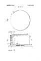
- the beam is assumed for convenience to be pointing vertically upwards and emergesthrough the outer polepiece P of the final or objective lens, of the electromagnetic type in the version illustrated. It impinges on a small area (a few microns across) of a. specimen S which, in the version illustrated, has its surface perpendicular to the beam.
- the impact of these primary electrons which may have energies of the order of 20 KeV, causes the emission of low-energy secondary electrons, with energies of only a few electron volts.
- the specimen surface, the pole-piece P and the cylindrical shield C form a hollow cylindrical drum with its ends at volts and its curved surface at a positive potential and the resulting electrostatic field is a rotationally symmetrical one with a saddle point at the center.
- the electrons initially moving relatively slowly, have that component of their velocity which is parallel to the electron-optical axis increased by the field, so those electrons which were initially diverging anyway start to converge, but as they approach the pole-piece P they are retarded, the axial component of their velocity is reduced, ultimately to zero, and the positive potential on the shield C draws them outwards and actually reverses their axial component.
- the initial divergence of the electrons from the electron-optical axis after a slight initial convergence, is thus enhanced to a substantial extent. Any asymmetry in the distribution of their trajectories on initially leaving the point of impact is therefore enhanced and if the electrons are emerging predominantly over a certain sector they will strike predominantly the corresponding sector of the shield C.
- the shield need not be circular in cross-section.
- the member P need not be the pole-piece itself but could be an earthed plate covering the pole-piece.
- the specimen may be covered by a flat disc-like earthed shield (with a small opening to expose that part of the specimen on which the beam impinges) to ensure predictable field conditions.
- the overall result could be achieved (though less predictably) with a specimen of small dimensions and no such earthed shield.
- the gauze G that forms the entry cage for a detector D in the form of a scintillator; this gauze extends the greater part of the axial length of the shield and circumferentially it extends over an arc of, say, between 60 and 120, and in a typical example it extends over
- the gauze is at the same potential as the shield C and thus does not upset the symmetry of the field.
- the scintillator itself can be at the usual high potential of several kilovolts, and can lead through a light pipe to a photomultiplier (not shown) to produce an electrical signal proportional to the number of electrons passing through the gauze.
- the detector D will pick up, and produce a signal from, those electrons which fall in that sector of the shield C which is occupied by the gauze.
- any contrast due to asymmetry in the direction in which the electrons leave the point of impact on the specimen surface is observed as a change in signal strength in the detector D.
- the detector arrangement according to the invention will still, like known detectors, show contrast due to differences in secondary emission coefficient.
- the shield C will normally be of metal. All the components may have a thin coating of carbon to reduce the emission ofspurious unwanted secondary electrons generated by the impact on them of high-energy primary electrons backscattered from the point of impact. Such a coating is particularly useful where the components are small in size.
- the entry gauze or cage G of the detector extends the greater part of the axial length of the shield C. It would be possible, in a modification, to restrict it, preferably in an adjustable manner, so that only the electrons picked up over a selected part of the axial length of the shield enter the detector. This can be done by blanking off part of the gauze G. The signal in the detector will then represent the number of electrons of only certain energy/direction combinations.
- the mode of operation shown in FIG. 1 is the simplest and the easiest to understand. It is suitable for observing topography of the specimen surface.
- a different mode shown in FIG. 3.
- the pole-piece remains at earth potential but the specimen is now at -I20 volts.
- the shield is at earth potential.
- the plate A is, in atypical case, at 80 volts.
- the gauze G of the detector is at a positive potential, for example +200 volts.
- a specimen containing magnetic domains may have a magnetic field close to its surface in any direction, i.e., having a component normal to the surface and having components in two directions parallel to the surface.
- the electrode system of FIG. 3 produces in effect two superimposed electrostatic fields having a divergent effect on the electron trajectories, one field being between the specimen surface and the plate A (which is 40 volts positive with respect to it), and the other field being between the specimen surface and the shield C (which is 120 volts positive with respect to it). It is only the components of the magnetic field parallel to the specimen surface that produce asymmetry of direction of the electron paths, and so this mode of operation is suitable for observing the components of magnetic field in this direction, not the component normal to the sur face. It is also suitable for observing electric fields parallel to the specimen surface.
- the detector gauze G is at a higher potential than the shield C and so introduces some asymmetry itself, but this has little influence on the important part of the field, namely at the specimen surface, and so although it does reduce directional contrast to some extent it is not serious.
- the detector is not sensitive to moderate changes in the energy of the electrons, and so potential contrast does not occur simultaneously with sensitivity to lateral electric and magnetic fields.
- the third mode of operation is particularly suitable for observing electric potential contrast.
- the electrode layout is the same as in FIG. 3, but the potentials are different.
- the specimen S and the shield C are now both at earth potential, as well as the pole-piece P, and the plate A is at a negative potential of variable value, being --36 volts in a particular example.
- the gauze G of the detector is again at +200 volts.
- the resulting retarding field (since the plate A is now negative with respect to the specimen surface) removes almost all of the directional information from the signal, and although it causes the electrons to diverge, it is the retarding effect that is predominant. Contrast in electrical potential between different regions of the specimen surface scanned will produce changes in the electrical signal that are monotonic, i.e., there are no maxima or minima in the relationship (within the normal working range) and so there is a direct and continuous relationship between specimen surface potential and signal strength. By varying the potential on the electrode A we can control the symmetry of the relationship.
- An additional ring-shaped electrode R shown in broken lines in FIG. 4, may be introduced close to the specimen surface and can carry a negative bias to vary the shape of the relationship between the potential on the specimen and the signal in the detector, and thereby to improve the linearity of this relationship.
- the mode shown in FIG. 4 is particularly suitable for observing the behavior of micro-circuits.
- a linear signal characteristic we can measure D.C. voltages and A.C. waveforms on a micro-circuit or circuit elements with only low distortion.
- the beam need not impinge on the specimen surface normally, but on the contrary operation at any angle from 0 to is possible, with the whole detector/shield system (including the scintillator) rotated.
- a metal plate with a small hole or slot for entry of the electron beam will replace the pole-piece as the body defining that end of the divergent field region which is opposite the specimen.
- the disc-like insert will then be fitted in the center of this plate.
- the invention is used with an electron beam scanning a selected small region of the specimen surface in synchronism with a cathode ray tube display of the contrast signal
- the invention could be used equally well with timevarying phenomena, using for example a stationary spot or a line scan in one dimension. Where the phenomenon varies in a regular periodic manner stroboscopic techniques may be employed; this is of particular value in examining alternating current waveforms at a selected point in the surface of a microcircuit.
- the fields that cause the electron trajectories to diverge and/or to be retarded have been shown as electrostatic in the examples described. However, they could be modified by the superposition of magnetic fields, produced by suitably placed permanent magnets or by electro-magnets. It is a general rule that effects which are obtainable electrostatically can also be obtained by the use of magnetic fields, although they may be less easy to design. It may even be possible to produce a wholly magnetic field to give the required divergent effect, effect by the use of two axially spaced toroidally wound electro-magnets replacing the shield C.
- Electron beam apparatus comprising means for generating a high energy beam of electrons, a specimen stage in the path of said beam, designed to receive a specimen for impingement thereon of said beam, and means for detecting secondary electrons emitted by and diverging from said specimen as a consequence of said impingement, wherein the improvement lies in the provision of guiding means for controlling the path of said secondary electrons from the specimen to the detecting means, said guiding means comprising an electrode structure creating a divergent electrostatic field in the path of said secondary electrons from said specimen, said field being selected to cause said secondary electrons of a given energy and following different paths from said specimen to spread out to a greater degree than they would do in the absence of said field thereby increasing the mutual divergence of said paths so as to accentuate differences in the trajectories of said secondary electrons, said detecting means occupying only a fraction of the solid angle over which the secondary electrons which are subjected to the increased divergence are spread.
- said guiding means comprise a hollow cylindrical shield, said shield being disposed with the axis thereof substantially normal to the surface of said specimen at the point of impingement of said beam.
- said guiding means further comprise a disc-shaped electrode, said electrode being disposed with its axis coincident with the axis of said shield and being disposed at the opposite end of said shield from said specimen.
- Electron beam apparatus comprising means for generating a beam of electrons, a specimen stage designed to receive a specimen for impingement thereon of said beam, means for detecting secondary electrons emitted by said specimen as a consequence of said impingement and guiding means for said secondary electrons, said guiding means creating a divergent electrostatic field in the path of said secondary electrons from said specimen such as to cause said secondary electrons of a given energy to spread out, accentuating differences in the trajectories thereof, said guiding means comprising first a hollow cylindrical shield, said shield being disposed with the axis thereof substantially normal to the surface of said specimen at the point of impingement of said beam, secondly a disc-shaped electrode disposed with its axis coincident with the axis of said shield and at the opposite end of said shield from said specimen, and thirdly a ring-shaped electrode adjacent said shield and between said shield and said specimen, said ring-shaped electrode being at an electric potential which is negative with respect to said specimen whereas said first-mentioned disc-
- a method of analyzing the secondary electrons emerging from the point of impact of an electron beam on a specimen comprising the steps of subjecting said secondary electrons to a divergent field that acts to accentuate the different trajectories of secondary electrons of the same energy whereby said secondary electrons diverge from one another over a substantial solid angle, and detecting the secondary electrons over only a fraction of said solid angle.
Landscapes
- Chemical & Material Sciences (AREA)
- Analytical Chemistry (AREA)
- Measurement Of Radiation (AREA)
- Analysing Materials By The Use Of Radiation (AREA)
Applications Claiming Priority (1)
| Application Number | Priority Date | Filing Date | Title |
|---|---|---|---|
| GB585569 | 1969-02-01 |
Publications (1)
| Publication Number | Publication Date |
|---|---|
| US3694652A true US3694652A (en) | 1972-09-26 |
Family
ID=9803896
Family Applications (1)
| Application Number | Title | Priority Date | Filing Date |
|---|---|---|---|
| US7198A Expired - Lifetime US3694652A (en) | 1969-02-01 | 1970-01-30 | Electron probe apparatus using an electrostatic field to cause secondary electrons to diverge |
Country Status (5)
| Country | Link |
|---|---|
| US (1) | US3694652A (ja) |
| JP (1) | JPS4830180B1 (ja) |
| DE (1) | DE2004256C3 (ja) |
| GB (1) | GB1304344A (ja) |
| NL (1) | NL7001404A (ja) |
Cited By (9)
| Publication number | Priority date | Publication date | Assignee | Title |
|---|---|---|---|---|
| US3961190A (en) * | 1975-03-06 | 1976-06-01 | International Business Machines Corporation | Voltage contrast detector for a scanning electron beam instrument |
| FR2488044A1 (fr) * | 1979-06-28 | 1982-02-05 | Jeol Ltd | Dispositif pour detecter des electrons secondaires dans un microscope electronique a balayage |
| US4442355A (en) * | 1980-07-31 | 1984-04-10 | Jeol, Ltd. | Device for detecting secondary electrons in a scanning electron microscope |
| US4683376A (en) * | 1984-09-18 | 1987-07-28 | ICT Integrated Circuit Testing Gesellschaft, fuer Halbleiterpruftechnik mbH | Opposing field spectrometer for electron beam mensuration technology |
| US4829243A (en) * | 1988-02-19 | 1989-05-09 | Microelectronics And Computer Technology Corporation | Electron beam testing of electronic components |
| US4943769A (en) * | 1989-03-21 | 1990-07-24 | International Business Machines Corporation | Apparatus and method for opens/shorts testing of capacitively coupled networks in substrates using electron beams |
| US6365896B1 (en) * | 1997-12-08 | 2002-04-02 | Philips Electron Optics B.V. | Environmental SEM with a magnetic field for improved secondary electron direction |
| US6730906B2 (en) | 1998-01-26 | 2004-05-04 | Applied Materials, Inc. | Method and apparatus for testing a substrate |
| US20130001419A1 (en) * | 2011-07-01 | 2013-01-03 | Taiwan Semiconductor Manufacturing Company, Ltd. | System and method for electromagnetic interferece shielding for critical dimension-scanning electron microscope |
Families Citing this family (3)
| Publication number | Priority date | Publication date | Assignee | Title |
|---|---|---|---|---|
| US4748324A (en) * | 1985-05-31 | 1988-05-31 | Siemens Aktiengesellschaft | Electrostatic opposing field spectrometer for electron beam test methods |
| GB2215907B (en) * | 1987-07-14 | 1992-04-15 | Jeol Ltd | Apparatus using a charged-particle beam |
| GB2229854B (en) * | 1989-03-28 | 1993-10-27 | Robinson Vivian N E | Backscattered electron detector |
Citations (3)
| Publication number | Priority date | Publication date | Assignee | Title |
|---|---|---|---|---|
| US2418228A (en) * | 1943-10-08 | 1947-04-01 | Rca Corp | Electronic microanalyzer |
| US3445708A (en) * | 1967-02-06 | 1969-05-20 | Gen Electric | Electron diffraction unit |
| US3474245A (en) * | 1965-06-23 | 1969-10-21 | Hitachi Ltd | Scanning electron microscope |
-
1969
- 1969-02-01 GB GB585569A patent/GB1304344A/en not_active Expired
-
1970
- 1970-01-30 NL NL7001404A patent/NL7001404A/xx unknown
- 1970-01-30 US US7198A patent/US3694652A/en not_active Expired - Lifetime
- 1970-01-30 DE DE2004256A patent/DE2004256C3/de not_active Expired
- 1970-01-31 JP JP45008394A patent/JPS4830180B1/ja active Pending
Patent Citations (3)
| Publication number | Priority date | Publication date | Assignee | Title |
|---|---|---|---|---|
| US2418228A (en) * | 1943-10-08 | 1947-04-01 | Rca Corp | Electronic microanalyzer |
| US3474245A (en) * | 1965-06-23 | 1969-10-21 | Hitachi Ltd | Scanning electron microscope |
| US3445708A (en) * | 1967-02-06 | 1969-05-20 | Gen Electric | Electron diffraction unit |
Cited By (12)
| Publication number | Priority date | Publication date | Assignee | Title |
|---|---|---|---|---|
| US3961190A (en) * | 1975-03-06 | 1976-06-01 | International Business Machines Corporation | Voltage contrast detector for a scanning electron beam instrument |
| FR2488044A1 (fr) * | 1979-06-28 | 1982-02-05 | Jeol Ltd | Dispositif pour detecter des electrons secondaires dans un microscope electronique a balayage |
| US4442355A (en) * | 1980-07-31 | 1984-04-10 | Jeol, Ltd. | Device for detecting secondary electrons in a scanning electron microscope |
| US4683376A (en) * | 1984-09-18 | 1987-07-28 | ICT Integrated Circuit Testing Gesellschaft, fuer Halbleiterpruftechnik mbH | Opposing field spectrometer for electron beam mensuration technology |
| US4829243A (en) * | 1988-02-19 | 1989-05-09 | Microelectronics And Computer Technology Corporation | Electron beam testing of electronic components |
| US4943769A (en) * | 1989-03-21 | 1990-07-24 | International Business Machines Corporation | Apparatus and method for opens/shorts testing of capacitively coupled networks in substrates using electron beams |
| US6365896B1 (en) * | 1997-12-08 | 2002-04-02 | Philips Electron Optics B.V. | Environmental SEM with a magnetic field for improved secondary electron direction |
| US6730906B2 (en) | 1998-01-26 | 2004-05-04 | Applied Materials, Inc. | Method and apparatus for testing a substrate |
| US20130001419A1 (en) * | 2011-07-01 | 2013-01-03 | Taiwan Semiconductor Manufacturing Company, Ltd. | System and method for electromagnetic interferece shielding for critical dimension-scanning electron microscope |
| US8633439B2 (en) * | 2011-07-01 | 2014-01-21 | Taiwan Semiconductor Manufacturing Company, Ltd. | System and method for electromagnetic interference shielding for critical dimension-scanning electron microscope |
| US20140124667A1 (en) * | 2011-07-01 | 2014-05-08 | Taiwan Semiconductor Manufacturing Company, Ltd. | System And Method For Electromagnetic Interference Shielding For Critical Dimension-Scanning Electron Microscope |
| US8952330B2 (en) * | 2011-07-01 | 2015-02-10 | Taiwan Semiconductor Manufacturing Company, Ltd. | System and method for electromagnetic interference shielding for critical dimension-scanning electron microscope |
Also Published As
| Publication number | Publication date |
|---|---|
| JPS4830180B1 (ja) | 1973-09-18 |
| DE2004256A1 (de) | 1970-08-06 |
| GB1304344A (ja) | 1973-01-24 |
| DE2004256B2 (de) | 1973-03-29 |
| DE2004256C3 (de) | 1973-10-18 |
| NL7001404A (ja) | 1970-08-04 |
Similar Documents
| Publication | Publication Date | Title |
|---|---|---|
| US10777382B2 (en) | Low voltage scanning electron microscope and method for specimen observation | |
| US6667476B2 (en) | Scanning electron microscope | |
| US6392231B1 (en) | Swinging objective retarding immersion lens electron optics focusing, deflection and signal collection system and method | |
| US6825475B2 (en) | Deflection method and system for use in a charged particle beam column | |
| EP0138610B1 (en) | Electron detector | |
| US6943349B2 (en) | Multi beam charged particle device | |
| JP3786875B2 (ja) | 帯電粒子ビームデバイスのための対物レンズ | |
| Pawley | Low voltage scanning electron microscopy | |
| US5493116A (en) | Detection system for precision measurements and high resolution inspection of high aspect ratio structures using particle beam devices | |
| US3694652A (en) | Electron probe apparatus using an electrostatic field to cause secondary electrons to diverge | |
| EP0918350A1 (en) | A scanning electron microscope and method for controlling a scanning electron microscope | |
| US5408098A (en) | Method and apparatus for detecting low loss electrons in a scanning electron microscope | |
| KR20220153059A (ko) | 다수의 검출기를 갖는 하전 입자 빔 장치 및 이미징 방법 | |
| WO2015016040A1 (ja) | 走査電子顕微鏡 | |
| JP2000200579A (ja) | 走査形電子顕微鏡 | |
| JPS61288357A (ja) | 定量的電位測定用スペクトロメ−タ−対物レンズ装置 | |
| US6504164B2 (en) | Electron beam apparatus | |
| US6897442B2 (en) | Objective lens arrangement for use in a charged particle beam column | |
| US6646261B2 (en) | SEM provided with a secondary electron detector having a central electrode | |
| US3646344A (en) | Scanning electron beam apparatus for viewing potential distribution on specimen surfaces | |
| JP6880209B2 (ja) | 走査電子顕微鏡 | |
| JP6736756B2 (ja) | 荷電粒子線装置 | |
| EP1160825A1 (en) | Particle beam apparatus | |
| Autrata et al. | Detectors for low voltage scanning electron microscopy | |
| JP2001148232A (ja) | 走査形電子顕微鏡 |