US20140327465A1 - Structures and methods for testing integrated circuits and via chains therein - Google Patents
Structures and methods for testing integrated circuits and via chains therein Download PDFInfo
- Publication number
- US20140327465A1 US20140327465A1 US13/875,962 US201313875962A US2014327465A1 US 20140327465 A1 US20140327465 A1 US 20140327465A1 US 201313875962 A US201313875962 A US 201313875962A US 2014327465 A1 US2014327465 A1 US 2014327465A1
- Authority
- US
- United States
- Prior art keywords
- via chain
- chain
- vias
- region
- constant current
- Prior art date
- Legal status (The legal status is an assumption and is not a legal conclusion. Google has not performed a legal analysis and makes no representation as to the accuracy of the status listed.)
- Granted
Links
Images
Classifications
-
- G—PHYSICS
- G01—MEASURING; TESTING
- G01R—MEASURING ELECTRIC VARIABLES; MEASURING MAGNETIC VARIABLES
- G01R31/00—Arrangements for testing electric properties; Arrangements for locating electric faults; Arrangements for electrical testing characterised by what is being tested not provided for elsewhere
- G01R31/28—Testing of electronic circuits, e.g. by signal tracer
- G01R31/2851—Testing of integrated circuits [IC]
- G01R31/2853—Electrical testing of internal connections or -isolation, e.g. latch-up or chip-to-lead connections
-
- H—ELECTRICITY
- H10—SEMICONDUCTOR DEVICES; ELECTRIC SOLID-STATE DEVICES NOT OTHERWISE PROVIDED FOR
- H10P—GENERIC PROCESSES OR APPARATUS FOR THE MANUFACTURE OR TREATMENT OF DEVICES COVERED BY CLASS H10
- H10P74/00—Testing or measuring during manufacture or treatment of wafers, substrates or devices
- H10P74/27—Structural arrangements therefor
- H10P74/277—Circuits for electrically characterising or monitoring manufacturing processes, e.g. circuits in tested chips or circuits in testing wafers
Definitions
- the technical field generally relates to structures and methods for testing integrated circuits, and more particularly relates to structures and methods for testing via chains in integrated circuits with improved accuracy in via resistance measurements.
- Integrated circuits comprise a large number of individual circuit elements, such as transistors, capacitors and resistors. These elements are connected by means of electrically conductive features to form complex circuits, such as memory devices, logic devices, and microprocessors.
- Multiple conductive layers are formed over individual circuit elements in and on a semiconductor substrate and are typically separated from each other by insulating dielectric layers. The conductive layers are often selectively connected or “wired” together in order to allow for conduction of electricity in a desired pattern.
- One means of connecting conductive layers is through the formation of a via at an interconnection between conductive layers. Vias are channels or plugs of conductive material. Interconnections between multiple conductive layers may be formed by a series of vias, i.e., a via chain.
- vias have decreased in size such that measurement of via resistance is difficult.
- typical testing tools struggle to measure accurately in the microvolt ( ⁇ V) differential voltage range.
- noise and offset levels are substantial in the ⁇ V range.
- current cannot be raised to overcome the testing limitations as the vias under testing generally cannot carry high currents.
- high current densities lead to overheating and destruction of the vias.
- a structure for testing an integrated circuit includes a semiconductor substrate and first and second via chains disposed over the substrate.
- the via chains include a substantially same sequence of segments interconnected at N via regions by a respective first and second via arrangement.
- the first via arrangement includes M N first vias at each respective via region and the second via arrangement includes M N +K N second vias at each respective via region.
- the first via arrangement is different than the second via arrangement and K N ⁇ 1 for at least one via region.
- the structure includes a voltage sensing apparatus in electrical connection with each via chain and configured to drive a first constant current through the first via chain and to drive a second constant current through the second via chain to measure a differential voltage between the via chains.
- a structure for testing a via chain.
- the structure includes a first via chain having N via regions, wherein each via region includes M N vias.
- the structure further includes a second via chain having N via regions, wherein each via region includes M N +K N vias.
- the structure includes a voltage sensing apparatus in electrical connection with each via chain and configured to drive a first constant current through the first via chain and to drive a second constant current through the second via chain to measure a differential voltage between the first via chain and the second via chain.
- a method for testing an integrated circuit includes providing a semiconductor substrate disposed with a first via chain and a second via chain.
- the first via chain includes a first sequence of segments interconnected at N via regions by a first via arrangement, wherein the first via arrangement includes a selected number of first vias at each respective via region in the first via chain.
- the second via chain includes a second sequence of segments interconnected at N via regions by a second via arrangement different from the first via arrangement, wherein the second via arrangement includes a selected number of second vias at each respective via region in the second via chain.
- the second sequence of segments is substantially the same as the first sequence of segments.
- the method includes driving a first constant current through the first via chain and driving a second constant current equal to the first constant current through the second via chain.
- the method further includes calculating a resistance of the vias in the first via chain.
- FIG. 1 is a cross sectional view of a via chain formed over a semiconductor substrate in accordance with an exemplary embodiment
- FIG. 2 is a schematic layout view of a structure for testing an integrated circuit utilizing a first via chain and a second via chain in accordance with an exemplary embodiment
- FIG. 3 is a schematic layout view of an alternate embodiment of a structure for testing an integrated circuit
- FIG. 4 is a schematic layout view of another alternate embodiment of a structure for testing an integrated circuit
- FIG. 5 is a schematic layout view illustrating the interconnection of conductive segments at a via region with a selected arrangement of vias in accordance with an embodiment herein;
- FIG. 6 is a schematic layout view illustrating the interconnection of conductive segments at a via region with an alternate arrangement of vias in accordance with another embodiment herein.
- a via chain includes a sequence of conductive segments, e.g., metal layers, interconnected by via regions. Because voltage differential is higher across via chains than across individual vias, it is more easily and accurately measured for via chains.
- parasitic resistance is typically a problem when measuring differential voltage across a path including conductive segments.
- problems associated with the measurement of parasitic resistance are avoided by testing two via chains having substantially same conductive segment sequences. Comparison of a differential voltage across the two via chains allows for cancellation of parasitic resistance.
- the interconnecting via regions are provided with different numbers of vias.
- the first via chain has a selected number of fewer vias than the second via chain.
- a difference in voltage differential across the first via chain and the second via chain is solely attributable to the difference in the number of vias. Therefore, the resistance of the vias may be calculated from the difference in voltage differentials across the via chains.
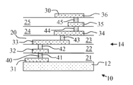
- FIG. 1 illustrates an exemplary integrated circuit 10 including semiconductor devices (not shown) formed in and/or on a semiconductor substrate 12 and a via chain 14 formed over the semiconductor substrate 12 .
- dielectric layers 20 such as layers 21 , 22 , 23 , 24 and 25 , are formed over the semiconductor substrate 12 .
- conductive layer segments 30 such as metal segments, are formed over the semiconductor substrate 12 and over each dielectric layer 20 to form an interconnect structure.
- segment 31 is formed over the semiconductor substrate 12
- segment 32 is formed over dielectric layer 21
- segment 33 is formed over dielectric layer 22
- segment 34 is formed over dielectric layer 23
- segment 35 is formed over dielectric layer 24
- segment 36 is formed over dielectric layer 25 .
- the conductive layer segments 30 are electrically interconnected by via regions 40 . Specifically, via region 41 electrically connects segments 31 and 32 , via region 42 electrically connects segments 32 and 33 , via region 43 electrically connects segments 33 and 34 , via region 44 electrically connects segments 34 and 35 , and via region 45 electrically connects segments 35 and 36 .
- the path from segment 31 to segment 36 is defined as via chain 14 .
- Via chains 14 may be formed in the device area of the integrated circuit 10 and in a testing area of the integrated circuit 10 .
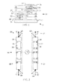
- FIG. 2 illustrates a testing structure 46 .
- the testing structure 46 includes two via chains 48 and 49 having substantially the same sequences of conductive layer segments 30 and via regions 40 .
- Physical layouts of the conductive layer segments 30 in the two via chains 48 and 49 are matched to have equivalent resistances.
- the two via chains 48 and 49 may have equivalent layouts on metal levels forming the conductive layer segments 30 , and subsections of via chains 48 and 49 alternate in the metal levels to enhance matching of manufactured characteristics.
- via chains 48 and 49 having the same number of conductive layer segments 30 formed from substantially the same conductive material and the same number of via regions 40 have substantially the same sequences.
- each via region 40 in via chain 48 includes one via 50 .
- each via region 40 in via chain 49 includes two vias 50 .
- Testing structure 46 includes a voltage sensing apparatus 60 connected to each via chain 48 and 49 .
- the exemplary voltage sensing apparatus 60 of FIG. 2 is a four-terminal or Kelvin sensing apparatus. Specifically, each exemplary voltage sensing apparatus 60 includes a first force connection 61 and a second force connection 62 . Further, each voltage sensing apparatus 60 is configured to drive a same constant current through each via chain 48 and 49 from first force connection 61 to second force connection 62 . Each voltage sensing apparatus 60 further includes a first sense connection 63 and a second sense connection 64 . Each sense connection 63 measures an applied voltage before the via chain 48 or 49 , and each sense connection 64 measures an applied voltage after the via chain 48 or 49 .
- the exemplary testing structure 46 further includes a controller 70 in communication with the sense connections 63 and 64 .
- the controller 70 may subtract the voltage measurement at each second sense connection 64 from the voltage measurement at each respective first sense connection 63 to find a respective voltage differential for each via chain 48 and 49 . Further, the controller 70 may calculate the resistance of the via chain 48 by comparing the voltage differentials of the via chains 48 and 49 as discussed below.
- the via chain 48 includes a single via 50 at each via region 40 and the via chain 49 includes two vias 50 at each via region 40
- the testing structure 46 need not be limited to such an embodiment. Rather, it is contemplated that the via chains 48 and 49 differ in number of vias 50 at at least one via region 40 , such as at two via regions 40 . Further, the number of vias 50 at selected via regions 40 need not be one or two, or differ by only one, but can be any practical number.
- An exemplary first via chain includes M N number of parallel vias at each N via region in the first via chain, where M N ⁇ 1.
- An exemplary second via chain includes M N +K N parallel vias at each N via region in the second via chain, where K N ⁇ 1 for at least one via region. At other via regions, K N may equal 0.
- V — sch ( If — sch )*( N*Rvia/M+Ra sum+ Rb sum)
- R via R_amp/( N *((1/ M N ) ⁇ 1/( K N +M N ))
- Improvement in calculating via resistance may be obtained when the first via chain includes a first via arrangement including M N first vias at each respective via region in the first via chain and the second via chain includes a second via arrangement different from the first via arrangement, such that the second via arrangement includes M N +K N second vias at each via region in the second via chain, wherein K N ⁇ 1 for at least one via region.
- the arrangement of via regions and vias may be selected upon simplicity, the desired calculation accuracy, or other factors.
- FIG. 3 an alternate embodiment of the testing structure 46 is illustrated.
- via chains 48 and 49 are connected in series and the voltage sensing apparatus 60 includes shared voltage and sense connections.
- the first force connection 61 is connected to the via chain 49 and the second force connection 62 is connected to the via chain 48 .
- the current from the first force connection 61 to second force connection 62 is driven through the via chains 49 and 48 . Therefore, the current is the same across the via chains 48 and 49 .
- the voltage sensing apparatus 60 includes a first sense connection 71 , a second sense connection 72 , and a third sense connection 73 .
- the first sense connection 71 measures an applied voltage before the via chain 49
- the second sense connection 72 measures an applied voltage after the via chain 49 and before the via chain 48
- the third sense connection 73 measures an applied voltage after the via chain 48 .
- a controller (not shown) may be used to calculate via resistance from the measurements taken by the sense connections 71 , 72 and 73 .
- FIG. 4 illustrates another embodiment of the testing structure 46 .
- the testing structure 46 uses an amplifier bridge structure 74 with a first series 75 of via chains 49 and 48 and a second parallel series 76 of via chains 48 and 49 .
- the voltage sensing apparatus 60 includes shared voltage and sense connections.
- the first force connection 61 and the second force connection 62 are connected to the parallel series 75 and 76 to drive a current equally through each series.
- the amplifier bridge structure 74 allows for the use of only two sense connections. Specifically, a first sense connection 78 measures an applied voltage after the via chain 49 in the first series 75 and a second sense connection 79 measures an applied voltage after the via chain 48 in the second series 76 .
- the amplifier bridge structure allows resistance measurement with a simple pad layout and quick “Force current—Measure voltage” test sequence with a subsequent step of dividing by N/4.
- the subtractive construction within the bridge structure reduces error factors because only one measurement is taken (hence error is introduced only once), and any relative error of the measurement equipment is applied directly on the (Vsch ⁇ Vdch) differential voltage (unlike by subsequent subtraction calculation processes where relative errors apply to the magnitude of Vsch and the Vdch, both of which are larger than the final result (Vsch ⁇ Vdch)).
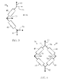
- FIG. 5 illustrates an exemplary interconnection of conductive layer segments 30 at a selected via region Z in via chains 48 and 49 .
- via chain 48 and via chain 49 each extend in a longitudinal direction 80 .
- the vias 50 in each via region 40 are arranged in a linear layout extending in a direction 82 substantially perpendicular to the longitudinal direction 80 .
- a via region 40 including more than two vias 50 is considered to have outer vias 84 .
- middle via(s) 86 is positioned between the outer vias 84 . Differences in parasitic resistance in the conductive layer segments 30 between via chains 48 and 49 are avoided by using the linear arrangement of vias 50 .
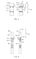
- FIG. 6 illustrates another exemplary interconnection of conductive layer segments 30 at a selected via region Z in via chains 48 and 49 .
- via chain 48 and via chain 49 each extend in a longitudinal direction 80 .
- the vias 50 in each via region 40 are arranged in a linear layout extending in a direction 88 substantially parallel or coincident to the longitudinal direction 80 .
- a via region 40 including more than two vias 50 is considered to have outer vias 84 .
- middle via(s) 86 is positioned between the outer vias 84 . Differences in parasitic resistance in the conductive layer segments 30 between via chains 48 and 49 are avoided by using the linear arrangement of vias 50 .
- the structures and methods for testing integrated circuits described herein utilize two via chains having substantially same sequences of conductive segments interconnected with via regions having different numbers of vias in at least one via region.
- the testing structures use four terminal resistance measurements to measure the resistances of the two via chains very accurately.
- the resistances of the via chains are provided with a higher sense measurement voltages (Vsense_high ⁇ Vsense_low) than those provided by testing a single via, and high differential voltage measurements enable accurate precision measurements using conventional measurement equipment. Further, by using the difference between the measured resistances (i.e., the difference between differential voltages), the parasitic content of the conductive segments are removed from the calculations.
- the current densities per via can be lowered and high current density induced measurement reproducibility problems can be minimized. Due to measuring multiple vias in series, the inherent averaging also enhances statistical accuracy of the mean value measurement of the via resistance.
Landscapes
- Engineering & Computer Science (AREA)
- Computer Hardware Design (AREA)
- Microelectronics & Electronic Packaging (AREA)
- General Engineering & Computer Science (AREA)
- Physics & Mathematics (AREA)
- General Physics & Mathematics (AREA)
- Semiconductor Integrated Circuits (AREA)
- Measurement Of Resistance Or Impedance (AREA)
- Automation & Control Theory (AREA)
- Manufacturing & Machinery (AREA)
- Testing Or Measuring Of Semiconductors Or The Like (AREA)
Abstract
Description
- The technical field generally relates to structures and methods for testing integrated circuits, and more particularly relates to structures and methods for testing via chains in integrated circuits with improved accuracy in via resistance measurements.
- Integrated circuits comprise a large number of individual circuit elements, such as transistors, capacitors and resistors. These elements are connected by means of electrically conductive features to form complex circuits, such as memory devices, logic devices, and microprocessors. Multiple conductive layers are formed over individual circuit elements in and on a semiconductor substrate and are typically separated from each other by insulating dielectric layers. The conductive layers are often selectively connected or “wired” together in order to allow for conduction of electricity in a desired pattern. One means of connecting conductive layers is through the formation of a via at an interconnection between conductive layers. Vias are channels or plugs of conductive material. Interconnections between multiple conductive layers may be formed by a series of vias, i.e., a via chain.
- During the formation of a via, problems may arise from high contact resistance between the via material and the region of the conductive layer to which it contacts, or through void or seam formation within the via. However, integrated circuit performance requires that the vias have substantially uniform resistances.
- Therefore, it is desirable to measure the resistances of vias to ensure proper integrated circuit performance. However, along with the miniaturization of device features of modern, ultra-high density integrated circuits, vias have decreased in size such that measurement of via resistance is difficult. Specifically, typical testing tools struggle to measure accurately in the microvolt (μV) differential voltage range. Further, noise and offset levels are substantial in the μV range. At the same time, current cannot be raised to overcome the testing limitations as the vias under testing generally cannot carry high currents. Specifically, high current densities lead to overheating and destruction of the vias. As a result, it is difficult to measure the resistance of vias that have low resistance and low current carrying capacity.
- Accordingly, it is desirable to provide improved structures and methods for testing integrated circuits and via chains therein. Further, it is desirable to provide structures and methods for measuring resistances of via chains in integrated circuits. Furthermore, other desirable features and characteristics will become apparent from the subsequent detailed description and the appended claims, taken in conjunction with the accompanying drawings and the foregoing technical field and background.
- Structures and methods for testing integrated circuits and via chains are provided. In an embodiment, a structure for testing an integrated circuit includes a semiconductor substrate and first and second via chains disposed over the substrate. The via chains include a substantially same sequence of segments interconnected at N via regions by a respective first and second via arrangement. The first via arrangement includes MN first vias at each respective via region and the second via arrangement includes MN+KN second vias at each respective via region. The first via arrangement is different than the second via arrangement and KN≧1 for at least one via region. The structure includes a voltage sensing apparatus in electrical connection with each via chain and configured to drive a first constant current through the first via chain and to drive a second constant current through the second via chain to measure a differential voltage between the via chains.
- In accordance with another embodiment, a structure is provided for testing a via chain. The structure includes a first via chain having N via regions, wherein each via region includes MN vias. The structure further includes a second via chain having N via regions, wherein each via region includes MN+KN vias. In the structure, KN≧2 for at least two via regions when MN=1; KN≧1 for at least three via regions when MN=1; or KN≧1 for at least seven via regions when MN=2. Also, the structure includes a voltage sensing apparatus in electrical connection with each via chain and configured to drive a first constant current through the first via chain and to drive a second constant current through the second via chain to measure a differential voltage between the first via chain and the second via chain.
- In another embodiment, a method for testing an integrated circuit is provided. The method includes providing a semiconductor substrate disposed with a first via chain and a second via chain. The first via chain includes a first sequence of segments interconnected at N via regions by a first via arrangement, wherein the first via arrangement includes a selected number of first vias at each respective via region in the first via chain. The second via chain includes a second sequence of segments interconnected at N via regions by a second via arrangement different from the first via arrangement, wherein the second via arrangement includes a selected number of second vias at each respective via region in the second via chain. Further, the second sequence of segments is substantially the same as the first sequence of segments. The method includes driving a first constant current through the first via chain and driving a second constant current equal to the first constant current through the second via chain. The method further includes calculating a resistance of the vias in the first via chain.
- Embodiments of structures for testing integrated circuits and via chains, and embodiments of methods for testing integrated circuits and via chains using such structures will be described in conjunction with the following drawing figures, wherein like numerals denote like elements, and wherein:
-
FIG. 1 is a cross sectional view of a via chain formed over a semiconductor substrate in accordance with an exemplary embodiment; -
FIG. 2 is a schematic layout view of a structure for testing an integrated circuit utilizing a first via chain and a second via chain in accordance with an exemplary embodiment; -
FIG. 3 is a schematic layout view of an alternate embodiment of a structure for testing an integrated circuit; -
FIG. 4 is a schematic layout view of another alternate embodiment of a structure for testing an integrated circuit; -
FIG. 5 is a schematic layout view illustrating the interconnection of conductive segments at a via region with a selected arrangement of vias in accordance with an embodiment herein; and -
FIG. 6 is a schematic layout view illustrating the interconnection of conductive segments at a via region with an alternate arrangement of vias in accordance with another embodiment herein. - The following detailed description is merely exemplary in nature and is not intended to limit the structures and methods for testing integrated circuits or via chains claimed herein. Furthermore, there is no intention to be bound by any expressed or implied theory presented in the preceding technical field, background or brief summary, or in the following detailed description.
- Structures and methods for testing integrated circuits and via chains as described herein avoid issues faced by current testing apparatuses. For example, current testing techniques often cannot measure accurately in the μV differential voltage range. To provide for improved testing and measurement, the structures and methods herein test via chains rather than individual vias. A via chain includes a sequence of conductive segments, e.g., metal layers, interconnected by via regions. Because voltage differential is higher across via chains than across individual vias, it is more easily and accurately measured for via chains.
- Further, the structures and methods herein avoid measurement problems typically encountered when measuring voltage differential across via chains. Specifically, parasitic resistance is typically a problem when measuring differential voltage across a path including conductive segments. Herein, problems associated with the measurement of parasitic resistance are avoided by testing two via chains having substantially same conductive segment sequences. Comparison of a differential voltage across the two via chains allows for cancellation of parasitic resistance.
- According to the embodiments herein, while the conductive segment sequences in the via chains are substantially the same, the interconnecting via regions are provided with different numbers of vias. Specifically, for at least one via region, the first via chain has a selected number of fewer vias than the second via chain. A difference in voltage differential across the first via chain and the second via chain is solely attributable to the difference in the number of vias. Therefore, the resistance of the vias may be calculated from the difference in voltage differentials across the via chains.
-
FIG. 1 illustrates an exemplaryintegrated circuit 10 including semiconductor devices (not shown) formed in and/or on asemiconductor substrate 12 and a viachain 14 formed over thesemiconductor substrate 12. As shown,dielectric layers 20, such aslayers semiconductor substrate 12. Further,conductive layer segments 30, such as metal segments, are formed over thesemiconductor substrate 12 and over eachdielectric layer 20 to form an interconnect structure. As shown,segment 31 is formed over thesemiconductor substrate 12,segment 32 is formed overdielectric layer 21,segment 33 is formed overdielectric layer 22,segment 34 is formed overdielectric layer 23,segment 35 is formed overdielectric layer 24, andsegment 36 is formed overdielectric layer 25. Theconductive layer segments 30 are electrically interconnected by viaregions 40. Specifically, viaregion 41 electrically connectssegments region 42 electrically connectssegments region 43 electrically connectssegments region 44 electrically connectssegments region 45 electrically connectssegments segment 31 tosegment 36 is defined as viachain 14. Viachains 14 may be formed in the device area of theintegrated circuit 10 and in a testing area of theintegrated circuit 10. -
FIG. 2 illustrates atesting structure 46. As shown, thetesting structure 46 includes two viachains conductive layer segments 30 and viaregions 40. Physical layouts of theconductive layer segments 30 in the two viachains chains conductive layer segments 30, and subsections of viachains chains conductive layer segments 30 formed from substantially the same conductive material and the same number of viaregions 40 have substantially the same sequences. As shown, each viaregion 40 in viachain 48 includes one via 50. Further, each viaregion 40 in viachain 49 includes twovias 50. -
Testing structure 46 includes avoltage sensing apparatus 60 connected to each viachain voltage sensing apparatus 60 ofFIG. 2 is a four-terminal or Kelvin sensing apparatus. Specifically, each exemplaryvoltage sensing apparatus 60 includes afirst force connection 61 and asecond force connection 62. Further, eachvoltage sensing apparatus 60 is configured to drive a same constant current through each viachain first force connection 61 tosecond force connection 62. Eachvoltage sensing apparatus 60 further includes afirst sense connection 63 and asecond sense connection 64. Eachsense connection 63 measures an applied voltage before the viachain sense connection 64 measures an applied voltage after the viachain - The
exemplary testing structure 46 further includes acontroller 70 in communication with thesense connections controller 70 may subtract the voltage measurement at eachsecond sense connection 64 from the voltage measurement at each respectivefirst sense connection 63 to find a respective voltage differential for each viachain controller 70 may calculate the resistance of the viachain 48 by comparing the voltage differentials of the viachains - While the via
chain 48 includes a single via 50 at each viaregion 40 and the viachain 49 includes twovias 50 at each viaregion 40, thetesting structure 46 need not be limited to such an embodiment. Rather, it is contemplated that the viachains vias 50 at at least one viaregion 40, such as at two viaregions 40. Further, the number ofvias 50 at selected viaregions 40 need not be one or two, or differ by only one, but can be any practical number. An exemplary first via chain includes MN number of parallel vias at each N via region in the first via chain, where MN≧1. An exemplary second via chain includes MN+KN parallel vias at each N via region in the second via chain, where KN≧1 for at least one via region. At other via regions, KN may equal 0. - Calculation of via resistance may be understood from discussion of a simplified testing structure that includes two via chains (or via chain sections) including conductive layer segments, such as alternating layers of metal A and metal B, interconnected by conductive vias to provide total of N number of transition or via regions between the conductive layer segments. While first via chains may include MN number of vias at each N via region in the first via chain, in a simplified testing structure MN=1 for each via region. While second via chains may include MN+KN number of vias at each N via region in the second via chain, in a simplified testing structure KN=1 for each via region.
- For the simplified testing structure (and wherein “sch” refers to a first via chain and “dch” refers to a second via chain):
-
V — sch=(If — sch)*(N*Rvia/M+Rasum+Rbsum) -
R — sch=V — sch/If — sch -
R — dch=V — dch/If — dch -
R_amp=Rsch−Rdch -
Rvia=R_amp/(N*((1/M N)−1/(K N +M N)) -
- where N is number of via
regions 40 in each via chain; - Rasum is the sum of resistances of metal A sections;
- Rbsum is the sum of resistances of metal B sections;
- If_sch and If_dch are the forced currents through the respective via chains;
- Pforce_high and Pforce_low are the force connections between which source power is applied;
- Rvia is the single via resistance; and
- R_amp is the calculated resistance difference between the first and the second chain.
- where N is number of via
- Thus, the difference in resistances between the two via chains gives the resistance value equivalent of N*((1/MN)−1/KN+MN)) vias. If MN=1 and KN=1 for all N via regions, this gives N/2 times the single via resistance. While the calculation becomes more complicated for testing structures having less simplified arrangement of vias, an equation for finding via resistance can be developed for any testing structure having two via chains with substantially same conductive segment sequences interconnected by varying, but known, arrangements of parallel vias. Improvement in calculating via resistance may be obtained when the first via chain includes a first via arrangement including MN first vias at each respective via region in the first via chain and the second via chain includes a second via arrangement different from the first via arrangement, such that the second via arrangement includes MN+KN second vias at each via region in the second via chain, wherein KN≧1 for at least one via region. In practice, improvement in resistance calculation has been found when KN≧2 for at least two via regions when MN=1 (assuming KN=0 for all other via regions) or when KN≧1 for at least three via regions when MN=1 (assuming KN=0 for all other via regions). Substantial improvement in resistance calculation has been found when KN≧1 for at least seven via regions when MN=2 (assuming KN=0 for all other via regions). The arrangement of via regions and vias may be selected upon simplicity, the desired calculation accuracy, or other factors.
- Referring now to
FIG. 3 , an alternate embodiment of thetesting structure 46 is illustrated. InFIG. 3 , viachains voltage sensing apparatus 60 includes shared voltage and sense connections. Specifically, thefirst force connection 61 is connected to the viachain 49 and thesecond force connection 62 is connected to the viachain 48. As a result, the current from thefirst force connection 61 tosecond force connection 62 is driven through the viachains chains - As shown, the
voltage sensing apparatus 60 includes afirst sense connection 71, asecond sense connection 72, and athird sense connection 73. Thefirst sense connection 71 measures an applied voltage before the viachain 49, thesecond sense connection 72 measures an applied voltage after the viachain 49 and before the viachain 48, and thethird sense connection 73 measures an applied voltage after the viachain 48. Similar toFIG. 2 , a controller (not shown) may be used to calculate via resistance from the measurements taken by thesense connections -
FIG. 4 illustrates another embodiment of thetesting structure 46. InFIG. 4 , thetesting structure 46 uses anamplifier bridge structure 74 with afirst series 75 of viachains parallel series 76 of viachains voltage sensing apparatus 60 includes shared voltage and sense connections. Specifically, thefirst force connection 61 and thesecond force connection 62 are connected to theparallel series amplifier bridge structure 74 allows for the use of only two sense connections. Specifically, afirst sense connection 78 measures an applied voltage after the viachain 49 in thefirst series 75 and a second sense connection 79 measures an applied voltage after the viachain 48 in thesecond series 76. - In the equations below, “sch” refers to via
chain 48 insecond series 76 and “dch” refers to viachain 49 infirst series 75. Further, for the simplifiedexemplary structure 74 ofFIGS. 4 , K=1 and M=1 for all via regions. For the amplifier bridge configuration of thetesting structure 46 inFIG. 4 : -
Vmeas=V — sch−V — dch=(N/4)*If*Rvia=(N/4)*Vvia -
Rvia=4*Vmeas/(N*If)=(Vmeas/If)/(N/4) -
- where:
- N is the number of via regions;
- M=1 and K=1 for all via regions;
- Vmeas is the differential voltage between via chains;
- V_sch is the resulting voltage after the via chain 48 (by forcing If current between
second force connection 62 and first force connection 61); and - V_dch is the resulting voltage after the via chain 49 (by forcing If current between
second force connection 62 and first force connection 61).
- Use of the amplifier bridge structure allows resistance measurement with a simple pad layout and quick “Force current—Measure voltage” test sequence with a subsequent step of dividing by N/4. The subtractive construction within the bridge structure reduces error factors because only one measurement is taken (hence error is introduced only once), and any relative error of the measurement equipment is applied directly on the (Vsch−Vdch) differential voltage (unlike by subsequent subtraction calculation processes where relative errors apply to the magnitude of Vsch and the Vdch, both of which are larger than the final result (Vsch−Vdch)).
-
FIG. 5 illustrates an exemplary interconnection ofconductive layer segments 30 at a selected via region Z in viachains chain 48 and viachain 49 each extend in alongitudinal direction 80. Further, thevias 50 in each viaregion 40 are arranged in a linear layout extending in adirection 82 substantially perpendicular to thelongitudinal direction 80. A viaregion 40 including more than twovias 50 is considered to haveouter vias 84. As shown, middle via(s) 86 is positioned between theouter vias 84. Differences in parasitic resistance in theconductive layer segments 30 between viachains vias 50. -
FIG. 6 illustrates another exemplary interconnection ofconductive layer segments 30 at a selected via region Z in viachains chain 48 and viachain 49 each extend in alongitudinal direction 80. Further, thevias 50 in each viaregion 40 are arranged in a linear layout extending in a direction 88 substantially parallel or coincident to thelongitudinal direction 80. A viaregion 40 including more than twovias 50 is considered to haveouter vias 84. As shown, middle via(s) 86 is positioned between theouter vias 84. Differences in parasitic resistance in theconductive layer segments 30 between viachains vias 50. - To briefly summarize, the structures and methods for testing integrated circuits described herein utilize two via chains having substantially same sequences of conductive segments interconnected with via regions having different numbers of vias in at least one via region. The testing structures use four terminal resistance measurements to measure the resistances of the two via chains very accurately. The resistances of the via chains are provided with a higher sense measurement voltages (Vsense_high−Vsense_low) than those provided by testing a single via, and high differential voltage measurements enable accurate precision measurements using conventional measurement equipment. Further, by using the difference between the measured resistances (i.e., the difference between differential voltages), the parasitic content of the conductive segments are removed from the calculations. Also, due to the increased sense measurement voltages, the current densities per via can be lowered and high current density induced measurement reproducibility problems can be minimized. Due to measuring multiple vias in series, the inherent averaging also enhances statistical accuracy of the mean value measurement of the via resistance.
- While at least one exemplary embodiment has been presented in the foregoing detailed description, it should be appreciated that a vast number of variations exist. It should also be appreciated that the exemplary embodiment or embodiments described herein are not intended to limit the scope, applicability, or configuration of the claimed subject matter in any way. Rather, the foregoing detailed description will provide those skilled in the art with a convenient road map for implementing the described embodiment or embodiments. It should be understood that various changes can be made in the function and arrangement of elements without departing from the scope defined by the claims, which includes known equivalents and foreseeable equivalents at the time of filing this patent application
Claims (20)
Priority Applications (3)
| Application Number | Priority Date | Filing Date | Title |
|---|---|---|---|
| US13/875,962 US9279851B2 (en) | 2013-05-02 | 2013-05-02 | Structures and methods for testing integrated circuits and via chains therein |
| TW102142936A TWI516779B (en) | 2013-05-02 | 2013-11-26 | Method and method for testing integrated circuit and through-hole chain therein |
| CN201410183441.XA CN104133170B (en) | 2013-05-02 | 2014-04-30 | Structure and method for testing integrated circuits and via chains therein |
Applications Claiming Priority (1)
| Application Number | Priority Date | Filing Date | Title |
|---|---|---|---|
| US13/875,962 US9279851B2 (en) | 2013-05-02 | 2013-05-02 | Structures and methods for testing integrated circuits and via chains therein |
Publications (2)
| Publication Number | Publication Date |
|---|---|
| US20140327465A1 true US20140327465A1 (en) | 2014-11-06 |
| US9279851B2 US9279851B2 (en) | 2016-03-08 |
Family
ID=51805915
Family Applications (1)
| Application Number | Title | Priority Date | Filing Date |
|---|---|---|---|
| US13/875,962 Expired - Fee Related US9279851B2 (en) | 2013-05-02 | 2013-05-02 | Structures and methods for testing integrated circuits and via chains therein |
Country Status (3)
| Country | Link |
|---|---|
| US (1) | US9279851B2 (en) |
| CN (1) | CN104133170B (en) |
| TW (1) | TWI516779B (en) |
Families Citing this family (1)
| Publication number | Priority date | Publication date | Assignee | Title |
|---|---|---|---|---|
| CN107481949B (en) * | 2017-06-20 | 2019-09-24 | 厦门市三安集成电路有限公司 | Monitor the method for one layer of dielectric coating process and its application in WAT Layout structure |
Citations (10)
| Publication number | Priority date | Publication date | Assignee | Title |
|---|---|---|---|---|
| US5900735A (en) * | 1996-10-31 | 1999-05-04 | Mitsubishi Denki Kabushiki Kaisha | Device for evaluating reliability of interconnect wires |
| US6570181B1 (en) * | 1999-12-07 | 2003-05-27 | Texas Instruments Incorporated | Semiconductor metal interconnect reliability test structure |
| US20040262604A1 (en) * | 2003-06-27 | 2004-12-30 | Jong-Hyun Lee | Test structure for detecting defect size in a semiconductor device and test method using same |
| US20050199875A1 (en) * | 2001-08-14 | 2005-09-15 | Eiichi Umemura | Inspection pattern, inspection method, and inspection system for detection of latent defect of multi-layer wiring structure |
| US20060220012A1 (en) * | 2005-03-31 | 2006-10-05 | Hsin-Chang Wu | Test key having a chain circuit and a kelvin structure |
| US20070111342A1 (en) * | 2000-04-18 | 2007-05-17 | Kla Tencor | Chemical mechanical polishing test structures and methods for inspecting the same |
| US20070296439A1 (en) * | 2006-05-31 | 2007-12-27 | Frank Feustel | Test structure for monitoring leakage currents in a metallization layer |
| US7919973B2 (en) * | 2007-06-22 | 2011-04-05 | Microchip Technology Incorporated | Method and apparatus for monitoring via's in a semiconductor fab |
| US20110221460A1 (en) * | 2010-03-10 | 2011-09-15 | Heinrich Trebo | Integrated Circuit Arrangement Having a Defect Sensor |
| US20130038334A1 (en) * | 2011-08-11 | 2013-02-14 | International Business Machines Corporation | Test structure, method and circuit for simultaneously testing time dependent dielectric breakdown and electromigration or stress migration |
Family Cites Families (7)
| Publication number | Priority date | Publication date | Assignee | Title |
|---|---|---|---|---|
| US7085977B2 (en) * | 2000-12-19 | 2006-08-01 | Texas Instruments Incorporated | Method and system for detecting an outlying resistance in a plurality of resistive elements |
| TWI388846B (en) * | 2005-07-14 | 2013-03-11 | Jsr Corp | An electrical impedance measuring device and a measuring method for connecting an electrical resistance measuring connector and a circuit board |
| US8067718B2 (en) | 2006-05-04 | 2011-11-29 | Tektronix, Inc. | Method and apparatus for probing |
| JP2007322127A (en) | 2006-05-30 | 2007-12-13 | Nidec-Read Corp | Method for inspecting substrate and substrate inspection system |
| JP2009070877A (en) * | 2007-09-11 | 2009-04-02 | Nec Electronics Corp | Semiconductor device and method for evaluating semiconductor device |
| CN101762750B (en) * | 2008-12-25 | 2011-10-26 | 上海北京大学微电子研究院 | Structure and method for measuring resistance of through hole |
| CN102200554A (en) * | 2011-03-30 | 2011-09-28 | 上海北京大学微电子研究院 | Resistor test structure and method |
-
2013
- 2013-05-02 US US13/875,962 patent/US9279851B2/en not_active Expired - Fee Related
- 2013-11-26 TW TW102142936A patent/TWI516779B/en not_active IP Right Cessation
-
2014
- 2014-04-30 CN CN201410183441.XA patent/CN104133170B/en not_active Expired - Fee Related
Patent Citations (10)
| Publication number | Priority date | Publication date | Assignee | Title |
|---|---|---|---|---|
| US5900735A (en) * | 1996-10-31 | 1999-05-04 | Mitsubishi Denki Kabushiki Kaisha | Device for evaluating reliability of interconnect wires |
| US6570181B1 (en) * | 1999-12-07 | 2003-05-27 | Texas Instruments Incorporated | Semiconductor metal interconnect reliability test structure |
| US20070111342A1 (en) * | 2000-04-18 | 2007-05-17 | Kla Tencor | Chemical mechanical polishing test structures and methods for inspecting the same |
| US20050199875A1 (en) * | 2001-08-14 | 2005-09-15 | Eiichi Umemura | Inspection pattern, inspection method, and inspection system for detection of latent defect of multi-layer wiring structure |
| US20040262604A1 (en) * | 2003-06-27 | 2004-12-30 | Jong-Hyun Lee | Test structure for detecting defect size in a semiconductor device and test method using same |
| US20060220012A1 (en) * | 2005-03-31 | 2006-10-05 | Hsin-Chang Wu | Test key having a chain circuit and a kelvin structure |
| US20070296439A1 (en) * | 2006-05-31 | 2007-12-27 | Frank Feustel | Test structure for monitoring leakage currents in a metallization layer |
| US7919973B2 (en) * | 2007-06-22 | 2011-04-05 | Microchip Technology Incorporated | Method and apparatus for monitoring via's in a semiconductor fab |
| US20110221460A1 (en) * | 2010-03-10 | 2011-09-15 | Heinrich Trebo | Integrated Circuit Arrangement Having a Defect Sensor |
| US20130038334A1 (en) * | 2011-08-11 | 2013-02-14 | International Business Machines Corporation | Test structure, method and circuit for simultaneously testing time dependent dielectric breakdown and electromigration or stress migration |
Also Published As
| Publication number | Publication date |
|---|---|
| TW201443456A (en) | 2014-11-16 |
| CN104133170B (en) | 2017-04-12 |
| TWI516779B (en) | 2016-01-11 |
| CN104133170A (en) | 2014-11-05 |
| US9279851B2 (en) | 2016-03-08 |
Similar Documents
| Publication | Publication Date | Title |
|---|---|---|
| US8350586B2 (en) | Method and apparatus of deembedding | |
| US7904273B2 (en) | In-line depth measurement for thru silicon via | |
| US8853693B2 (en) | Test structure for determination of TSV depth | |
| TWI601222B (en) | Integrated circuit test structure with monitoring chain and test leads | |
| US20090065947A1 (en) | Semiconductor device having circularly connected plural pads via through holes and method of evaluating the same | |
| US10068815B2 (en) | Test structure for testing via resistance and method | |
| JP5529611B2 (en) | Semiconductor device and resistance measuring method | |
| CN104658940A (en) | Structure for measuring electrical properties of FinFET (fin field-effect transistor) | |
| CN112864131A (en) | Electromigration test structure and electromigration test method | |
| US9279851B2 (en) | Structures and methods for testing integrated circuits and via chains therein | |
| US6383827B1 (en) | Electrical alignment test structure using local interconnect ladder resistor | |
| CN113782516B (en) | Electromigration test structure, electromigration test system, electromigration test memory, manufacturing method and test method | |
| TW201443449A (en) | Substrate inspecting apparatus and substrate inspecting method | |
| JP2008218921A (en) | Pattern for measuring misregistration amount, measuring method, and semiconductor device | |
| CN112230067B (en) | Resistance testing structure and method | |
| US7688083B2 (en) | Analogue measurement of alignment between layers of a semiconductor device | |
| KR102940128B1 (en) | Test Structure and Evaluation Method for Semiconductor Photo Overlay | |
| CN104282661B (en) | The test structure and its method of testing of fail-safe analysis in integrated circuit | |
| US20170363682A1 (en) | Testing system, method for testing an integrated circuit and a circuit board including the same | |
| CN104183574B (en) | Semiconductor testing structure and a semiconductor testing method | |
| ITTO991148A1 (en) | ELECTRONIC DEVICE WITH DOUBLE WIRE CONNECTIONS, METHOD OF MANUFACTURE OF SUCH ELECTRONIC DEVICE AND METHOD OF VERIFICATION OF THE | |
| EP4549898A1 (en) | Temperature sensor, temperature sensor packaging method, and temperature measurement method | |
| JP2011059085A (en) | Semiconductor device and method of inspecting the same | |
| Hess et al. | Digital tester-based measurement methodology for process control in multilevel metallization systems | |
| CN120784241A (en) | Test unit and test method |
Legal Events
| Date | Code | Title | Description |
|---|---|---|---|
| AS | Assignment |
Owner name: GLOBALFOUNDRIES INC., CAYMAN ISLANDS Free format text: ASSIGNMENT OF ASSIGNORS INTEREST;ASSIGNOR:CSASZAR, FARKAS MARTON;REEL/FRAME:030342/0031 Effective date: 20130423 |
|
| STCF | Information on status: patent grant |
Free format text: PATENTED CASE |
|
| AS | Assignment |
Owner name: WILMINGTON TRUST, NATIONAL ASSOCIATION, DELAWARE Free format text: SECURITY AGREEMENT;ASSIGNOR:GLOBALFOUNDRIES INC.;REEL/FRAME:049490/0001 Effective date: 20181127 |
|
| FEPP | Fee payment procedure |
Free format text: MAINTENANCE FEE REMINDER MAILED (ORIGINAL EVENT CODE: REM.); ENTITY STATUS OF PATENT OWNER: LARGE ENTITY |
|
| LAPS | Lapse for failure to pay maintenance fees |
Free format text: PATENT EXPIRED FOR FAILURE TO PAY MAINTENANCE FEES (ORIGINAL EVENT CODE: EXP.); ENTITY STATUS OF PATENT OWNER: LARGE ENTITY |
|
| STCH | Information on status: patent discontinuation |
Free format text: PATENT EXPIRED DUE TO NONPAYMENT OF MAINTENANCE FEES UNDER 37 CFR 1.362 |
|
| FP | Lapsed due to failure to pay maintenance fee |
Effective date: 20200308 |
|
| AS | Assignment |
Owner name: GLOBALFOUNDRIES INC., CAYMAN ISLANDS Free format text: RELEASE BY SECURED PARTY;ASSIGNOR:WILMINGTON TRUST, NATIONAL ASSOCIATION;REEL/FRAME:054636/0001 Effective date: 20201117 |
|
| AS | Assignment |
Owner name: GLOBALFOUNDRIES U.S. INC., NEW YORK Free format text: RELEASE BY SECURED PARTY;ASSIGNOR:WILMINGTON TRUST, NATIONAL ASSOCIATION;REEL/FRAME:056987/0001 Effective date: 20201117 Owner name: GLOBALFOUNDRIES U.S. INC., NEW YORK Free format text: RELEASE OF SECURITY INTEREST;ASSIGNOR:WILMINGTON TRUST, NATIONAL ASSOCIATION;REEL/FRAME:056987/0001 Effective date: 20201117 |