US20030193360A1 - Integrated circuit devices that provide constant time delays irrespective of temperature variation - Google Patents
Integrated circuit devices that provide constant time delays irrespective of temperature variation Download PDFInfo
- Publication number
- US20030193360A1 US20030193360A1 US10/357,695 US35769503A US2003193360A1 US 20030193360 A1 US20030193360 A1 US 20030193360A1 US 35769503 A US35769503 A US 35769503A US 2003193360 A1 US2003193360 A1 US 2003193360A1
- Authority
- US
- United States
- Prior art keywords
- resistance value
- integrated circuit
- resistor
- delay circuit
- internal node
- Prior art date
- Legal status (The legal status is an assumption and is not a legal conclusion. Google has not performed a legal analysis and makes no representation as to the accuracy of the status listed.)
- Granted
Links
Images


Classifications
-
- H—ELECTRICITY
- H03—ELECTRONIC CIRCUITRY
- H03K—PULSE TECHNIQUE
- H03K5/00—Manipulating of pulses not covered by one of the other main groups of this subclass
- H03K5/01—Shaping pulses
- H03K5/04—Shaping pulses by increasing duration; by decreasing duration
- H03K5/06—Shaping pulses by increasing duration; by decreasing duration by the use of delay lines or other analogue delay elements
-
- G—PHYSICS
- G11—INFORMATION STORAGE
- G11C—STATIC STORES
- G11C7/00—Arrangements for writing information into, or reading information out from, a digital store
- G11C7/22—Read-write [R-W] timing or clocking circuits; Read-write [R-W] control signal generators or management
- G11C7/222—Clock generating, synchronizing or distributing circuits within memory device
-
- G—PHYSICS
- G11—INFORMATION STORAGE
- G11C—STATIC STORES
- G11C7/00—Arrangements for writing information into, or reading information out from, a digital store
- G11C7/22—Read-write [R-W] timing or clocking circuits; Read-write [R-W] control signal generators or management
-
- H—ELECTRICITY
- H03—ELECTRONIC CIRCUITRY
- H03K—PULSE TECHNIQUE
- H03K5/00—Manipulating of pulses not covered by one of the other main groups of this subclass
- H03K5/01—Shaping pulses
- H03K5/08—Shaping pulses by limiting; by thresholding; by slicing, i.e. combined limiting and thresholding
- H03K5/082—Shaping pulses by limiting; by thresholding; by slicing, i.e. combined limiting and thresholding with an adaptive threshold
-
- H—ELECTRICITY
- H03—ELECTRONIC CIRCUITRY
- H03K—PULSE TECHNIQUE
- H03K5/00—Manipulating of pulses not covered by one of the other main groups of this subclass
- H03K5/13—Arrangements having a single output and transforming input signals into pulses delivered at desired time intervals
- H03K5/133—Arrangements having a single output and transforming input signals into pulses delivered at desired time intervals using a chain of active delay devices
-
- G—PHYSICS
- G11—INFORMATION STORAGE
- G11C—STATIC STORES
- G11C7/00—Arrangements for writing information into, or reading information out from, a digital store
- G11C7/04—Arrangements for writing information into, or reading information out from, a digital store with means for avoiding disturbances due to temperature effects
-
- H—ELECTRICITY
- H03—ELECTRONIC CIRCUITRY
- H03K—PULSE TECHNIQUE
- H03K5/00—Manipulating of pulses not covered by one of the other main groups of this subclass
- H03K2005/00013—Delay, i.e. output pulse is delayed after input pulse and pulse length of output pulse is dependent on pulse length of input pulse
- H03K2005/00078—Fixed delay
- H03K2005/00143—Avoiding variations of delay due to temperature
Definitions
- the present invention is related to integrated circuit devices and, more particularly, to integrated circuit devices including delay circuits that delay an input signal by a predetermined time.
- Signal delay circuits or pulse generating circuits have been used in integrated circuit devices for various purposes, such as signal control. Such signal delay or pulse generating circuits are typically formed using a delay circuit. Generally, the width of a pulse signal is dependant upon a delay time of a delay circuit. Accordingly, it may be important to control the delay time of the delay circuit in order to obtain an accurate pulse width.
- the delay time may be controlled using a time constant that is determined using the values of one or more resistors and capacitors in the delay circuit.
- a resistor may be formed of polysilicon, for example, a polysilicon resistor, and a capacitor may be formed using a gate capacitance of a transistor.
- the gate capacitance of the transistor is typically dependent upon the thickness of its gate oxide film, thus, possibly making it difficult to freely adjust the capacitance per the unit area.
- the area occupied by the capacitor in a chip may be relatively large as compared with the area occupied by the resistor. For this reason, gate capacitance is determined so as to ignore parasitic capacitance and the time constant of a delay circuit is adjusted using a resistor whose sheet resistance can be controlled relatively easily and whose chip area is small relative to the chip area of the capacitor.
- Embodiments of the present invention provide integrated circuit devices including delay circuits having first and second resistive elements electrically coupled in series having first and second resistance values.
- the first resistance value varies in proportion to temperature and the second resistance value varies in inverse proportion to temperature.
- the sum of the first and second resistance values may remain substantially constant as a temperature of the integrated circuit device increases and/or decreases.
- the ratio of the first resistance value to the second resistance value is 2:1.
- a change ratio of a resistance rate of change of the first resistive element to a resistance rate of change of the second resistive element is 1:2.
- the first and second resistive elements may include first and second resistors.
- the integrated circuit device may be an integrated circuit memory device.
- the memory device may include a flash memory device
- the first resistive element may comprise a floating gate of the flash memory device that includes lightly doped polysilicon
- the second resistive element may comprises a control gate of the flash memory device that includes highly doped polysilicon.
- the lightly doped polysilicon may have an impurity concentration of from about 1 ⁇ 10 16 to about 1 ⁇ 10 18 and the highly doped polysilicon may have an impurity concentration of about 1 ⁇ 10 20 .
- FIG. 1 is a circuit diagram illustrating integrated circuit devices according to embodiments of the present invention
- FIG. 2 is a diagram illustrating waveforms at nodes of integrated circuit devices according to embodiments of the present invention, for example, embodiments illustrated in FIG. 1;
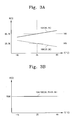
- FIG. 3A is a diagram illustrating resistance variation of resistive elements according to embodiments of the present invention in accordance with temperature variation.
- FIG. 3B is a diagram illustrating a sum of the resistance values of the resistive elements according to embodiments of the present invention as temperature varies.
- Embodiments of the present invention will be described below with respect to FIGS. 1 through 3B.
- Embodiments of the present invention provide delay circuits having a substantially constant time delay irrespective of temperature variation.
- a resistive means is provided having a substantially constant resistance value irrespective of temperature.
- the resistive means is provided by first and second resistive elements electrically coupled in series having first and second resistance values.
- the first resistance value varies in proportion to temperature and the second resistance value varies in inverse proportion to temperature.
- a sum of the first and second resistance values may remain substantially constant despite a variation in the temperature of the integrated circuit device.
- the ability to maintain a substantially constant resistance value may provide a substantially constant time delay for the integrated circuit device because a time constant of the integrated circuit device is partially based on the resistance of the integrated circuit.
- an integrated circuit device includes a delay circuit 100 .
- the delay circuit 100 receives an input signal IN and delays the input signal IN by a predetermined delay time.
- the delay circuit includes first, second and third inverters 102 , 112 , and 116 , a first resistor 104 , a second resistor 106 , a capacitor 108 , a PMOS transistor 110 , and a NAND gate 114 .
- the elements of the delay circuit 100 are electrically coupled as illustrated in FIG. 1.
- the first inverter 102 receives and inverts an input signal IN via an input terminal 120 .
- the first and second resistors 104 and 106 are connected in series between an output of the first inverter 102 and a first internal node ND 10 , and the capacitor 108 is connected between the first internal node ND 10 and a ground voltage VSS.
- the first and second resistors 104 and 106 are formed of polysilicon and the capacitor 108 is formed using gate capacitance of a MOS transistor.
- the first and second resistors 104 and 106 can be formed using an active region of a semiconductor substrate, i.e., an active resistor.
- the PMOS transistor 110 is coupled between a power supply voltage VCC and the first internal node ND 10 and is turned on/off by the input signal IN that is applied to the input terminal 120 .
- the second inverter 112 is connected between the first internal node ND 10 and a second internal node ND 20 .
- the input of the second inverter 112 is connected to the first internal node ND 10 and an output of the second inverter 112 is connected to the second internal node ND 20 .
- the NAND gate 114 has a first input terminal connected to receive the input signal IN and a second input terminal connected to the second internal node ND 20 .
- the third inverter 116 is connected between an output of the NAND gate 114 and an output terminal 122 for outputting an output signal OUT.
- first and second resistors 104 and 106 are not limited to this configuration; alternatively, the first and second resistors 104 and 106 may be replaced by any element that provides a resistive means.
- the capacitor 108 and the PMOS transistor 110 may be replaced with any element that provides the same or similar functionality without departing from the teachings of the present invention.
- FIG. 2 a waveform diagram illustrating operations of integrated circuits according to embodiments of the present invention illustrated in FIG. 1 will be discussed.
- charge current from a pull-up transistor (not shown) of the first inverter 102 flows into the first internal node ND 10 via the first and second resistors 104 and 106 .
- the capacitor 108 coupled to the first internal node ND 10 is charged.
- the pull-up transistor of the first inverter 102 and the first and second resistors 104 and 106 form a charge path of the capacitor 108 .
- the PMOS transistor 110 is turned on, charge current from the transistor 110 is supplied to the capacitor 108 that is connected to the first internal node ND 10 . Since the second internal node ND 20 is at the low level, the output signal OUT goes low.
- a pull-down transistor (not shown) of the first inverter 102 is turned on instead of the pull-up transistor (not shown) discussed above.
- the capacitor 108 discharges through the first and second resistors 104 and 106 and the pull-down transistor of the first inverter 102 .
- the pull-down transistor of the first inverter 102 and the first and second resistors 104 and 106 form a discharge path of the capacitor 108 .
- R is, for example, the sum of resistance values of the resistors 104 and 106
- C is a capacitance value of, for example, the capacitor 108 .
- the output signal of the second inverter 112 When the output signal of the second inverter 112 has a low-to-high transition, an output signal of the NAND gate 114 goes low. Accordingly, the output signal OUT transitions from a low level to a high level.
- the input signal IN may be delayed by, for example, about 10 nanoseconds (ns), before the output signal OUT transitions from the low level to the high level.
- the time constant (T) may be determined by the resistors 104 and 106 and the capacitor 108 .
- the larger the time constant that is determined by the resistors 104 and 106 and the capacitor 108 the longer the delay time of the input signal IN.
- the smaller the time constant the shorter the delay time of the input signal IN.
- a resistance value typically varies responsive to an increase and/or decrease in temperature.
- the time constant may vary responsive to the temperature variation because, as discussed above, the time constant is determined based partially upon the resistance value of the integrated circuit. Accordingly, the delay time of an input signal, for example, the input signal IN, may vary responsive to an increase and/or decrease in temperature.
- the first resistor 104 has a resistance value that varies in proportion to the temperature variation
- the second resistor 106 has a second resistance value that varies in inverse proportion to the temperature.
- the first resistor 104 may have a resistance variation of about 15% in a range of ⁇ 45° C. to +85° C.
- the second resistor 106 has a resistance variation of about ⁇ 30% in a range of ⁇ 45° C. to +85° C.
- a ratio of a resistance change rate of the first resistor 104 to a resistance change rate of the second resistor 106 is 1:2 with respect to the temperature variation. Under this condition, a ratio of a resistance value of the first resistor 104 to a resistance value of the second resistor 106 becomes 2:1.
- a resistor of 100 K ⁇ and a capacitor of 100 fF can be used to delay an input signal IN by about 10 ns. If this resistance value of 100 K ⁇ varies in accordance with temperature variation, a delay time of the conventional delay circuit also varies.
- Delay circuits may make it possible to obtain a substantially constant resistance value irrespective of the temperature variations by using, for example, first and second resistors 104 and 106 having different resistance variation characteristics from each other as discussed above. Accordingly, the first resistor 104 can be set to have a resistance value of about, for example, 66.7 K ⁇ , and the second resistor 106 can be set to have a resistance value of about, for example, 33.33 K ⁇ .
- a resistance value of the first resistor 104 may be varied by 10 K ⁇ that corresponds to 15% of 66.7 K ⁇
- a resistance value of the second resistor 106 may be varied by 10 K ⁇ that corresponds to ⁇ 30% of 33.3 K ⁇ .
- a constant resistance value may be obtained irrespective of temperature variation, by using the first resistor 104 having a resistance value that varies in proportion to the temperature and the second resistor 106 having a resistance value that varies in inverse proportion to the temperature.
- a delay time may also be substantially constant irrespective of changes in temperature. A substantially constant delay time may make it possible to control a signal more accurately and more finely.
- the delay circuit according to embodiments of the present invention may be included in many integrated circuit devices.
- the delay circuit according to embodiments of the present invention may be used in a pulse generating circuit.
- the delay circuit of the present invention may also be included in an integrated circuit memory device using a floating gate transistor, for example, a flash memory device.
- the delay circuit of the present invention can be used in a control circuit that controls operational timing of control signals of the flash memory device.
- a floating gate transistor comprises a source, a drain, a floating gate, and a control gate.
- the floating gate is used for storing charges and is formed of polysilicon that has a low impurity concentration, for example, polysilicon having an impurity concentration of from about 1 ⁇ 10 16 to about 1 ⁇ 10 18 .
- the control gate is formed of polysilicon that has a high impurity concentration, for example, polysilicon having an impurity concentration of about 1 ⁇ 10 20 .
- the first resistor 104 of the delay circuit can be formed of a lightly doped polysilicon that is used to form the floating gate of the floating gate transistor.
- the second resistor 106 of the delay circuit can be formed of a highly doped polysilicon that is used to form the control gate of the floating gate transistor.
- an integrated circuit device that includes resistive means that has a substantially constant resistance value irrespective of temperature variation.
- the resistive means includes at least two polysilicon resistors and that are electrically coupled in series with a charge/discharge path of a capacitor.
- One of the two polysilicon resistors has a resistance value that is increased or decreased when a temperature is increased or decreased, i.e. in proportion to the temperature variation.
- the other of the two polysilicon transistors has a resistance value that is increased or decreased when a temperature is decreased or increased, i.e. inversely proportional to the temperature variation.
- a sum of the resistance values of the polysilicon resistors is substantially constant. Accordingly it is possible to constantly maintain a resistance value of the resistive means irrespective of the temperature variation.
Landscapes
- Physics & Mathematics (AREA)
- Nonlinear Science (AREA)
- Pulse Circuits (AREA)
- Dram (AREA)
Abstract
A delay circuit is provided including first and second resistive elements electrically coupled in series having first and second resistance values. The first resistance value varies in proportion to temperature and the second resistance value varies in inverse proportion to temperature.
Description
- This application is related to and claims priority from Korean Application No. 2002-19946, filed on Apr. 12, 2002, the disclosure of which is hereby incorporated herein by reference as if set forth in its entirety.
- The present invention is related to integrated circuit devices and, more particularly, to integrated circuit devices including delay circuits that delay an input signal by a predetermined time.
- Signal delay circuits or pulse generating circuits have been used in integrated circuit devices for various purposes, such as signal control. Such signal delay or pulse generating circuits are typically formed using a delay circuit. Generally, the width of a pulse signal is dependant upon a delay time of a delay circuit. Accordingly, it may be important to control the delay time of the delay circuit in order to obtain an accurate pulse width. The delay time may be controlled using a time constant that is determined using the values of one or more resistors and capacitors in the delay circuit. A resistor may be formed of polysilicon, for example, a polysilicon resistor, and a capacitor may be formed using a gate capacitance of a transistor.
- The gate capacitance of the transistor is typically dependent upon the thickness of its gate oxide film, thus, possibly making it difficult to freely adjust the capacitance per the unit area. The area occupied by the capacitor in a chip may be relatively large as compared with the area occupied by the resistor. For this reason, gate capacitance is determined so as to ignore parasitic capacitance and the time constant of a delay circuit is adjusted using a resistor whose sheet resistance can be controlled relatively easily and whose chip area is small relative to the chip area of the capacitor.
- Unfortunately, since a polysilicon resistor is susceptible to temperature variation, it may be difficult to form a polysilicon resistor that has a constant resistance value as the temperature of the integrated circuit device increases and/or decreases. This variation in the resistance value of a polysilicon resistor caused by the temperature variation may, therefore, introduce inaccuracy into the control signals that are used in integrated circuit devices.
- Embodiments of the present invention provide integrated circuit devices including delay circuits having first and second resistive elements electrically coupled in series having first and second resistance values. The first resistance value varies in proportion to temperature and the second resistance value varies in inverse proportion to temperature.
- In some embodiments of the present invention, the sum of the first and second resistance values may remain substantially constant as a temperature of the integrated circuit device increases and/or decreases.
- In further embodiments of the present invention, the ratio of the first resistance value to the second resistance value is 2:1. In certain embodiments of the present invention, a change ratio of a resistance rate of change of the first resistive element to a resistance rate of change of the second resistive element is 1:2. The first and second resistive elements may include first and second resistors.
- In still further embodiments of the present invention, the integrated circuit device may be an integrated circuit memory device. In certain embodiments, the memory device may include a flash memory device, the first resistive element may comprise a floating gate of the flash memory device that includes lightly doped polysilicon and the second resistive element may comprises a control gate of the flash memory device that includes highly doped polysilicon. The lightly doped polysilicon may have an impurity concentration of from about 1×10 16 to about 1×10¹⁸ and the highly doped polysilicon may have an impurity concentration of about 1×10²⁰.
- FIG. 1 is a circuit diagram illustrating integrated circuit devices according to embodiments of the present invention;
- FIG. 2 is a diagram illustrating waveforms at nodes of integrated circuit devices according to embodiments of the present invention, for example, embodiments illustrated in FIG. 1;
- FIG. 3A is a diagram illustrating resistance variation of resistive elements according to embodiments of the present invention in accordance with temperature variation; and
- FIG. 3B is a diagram illustrating a sum of the resistance values of the resistive elements according to embodiments of the present invention as temperature varies.
- The present invention now will be described more fully with reference to the accompanying drawings, in which embodiments of the invention are shown. This invention may, however, be embodied in many different forms and should not be construed as being limited to the embodiments set forth herein; rather, these embodiments are provided so that this disclosure will be thorough and complete, and will fully convey the concept of the invention to those skilled in the art. In the drawings, when an element is referred to as being “connected” or “coupled” to another element, it can be directly connected or coupled to the other element or intervening elements may be present. In contrast, when an element is referred to as being “directly connected” or “directly coupled” to another element, there are no intervening elements present. Like reference numerals refer to like elements throughout.
- It will be understood that although terms such as first, second etc. are used herein to describe various elements, these elements should not be limited by these terms. These terms are only used to distinguish one element from another element. Thus, a first element discussed below could be termed a second element, and similarly, a second element may be termed a first element without departing from the teachings of the present invention.
- Embodiments of the present invention will be described below with respect to FIGS. 1 through 3B. Embodiments of the present invention provide delay circuits having a substantially constant time delay irrespective of temperature variation. A resistive means is provided having a substantially constant resistance value irrespective of temperature. In certain embodiments, the resistive means is provided by first and second resistive elements electrically coupled in series having first and second resistance values. In these embodiments, the first resistance value varies in proportion to temperature and the second resistance value varies in inverse proportion to temperature. Thus, a sum of the first and second resistance values may remain substantially constant despite a variation in the temperature of the integrated circuit device. The ability to maintain a substantially constant resistance value may provide a substantially constant time delay for the integrated circuit device because a time constant of the integrated circuit device is partially based on the resistance of the integrated circuit. In particular, the time constant (T) of the integrated circuit device is determined using the equation T=RC, where R is resistance value. Accordingly, integrated circuits according to embodiments of the present invention may provide substantially constant resistance values and/or signal delay times in the presence of temperature variation.
- Referring now to FIG. 1, a circuit diagram illustrating integrated circuit devices according to embodiments of the present invention will be discussed. As illustrated in FIG. 1, an integrated circuit device according to embodiments of the present invention includes a
delay circuit 100. Thedelay circuit 100 receives an input signal IN and delays the input signal IN by a predetermined delay time. The delay circuit includes first, second andthird inverters first resistor 104, asecond resistor 106, acapacitor 108, aPMOS transistor 110, and aNAND gate 114. The elements of thedelay circuit 100 are electrically coupled as illustrated in FIG. 1. - In particular, the
first inverter 102 receives and inverts an input signal IN via aninput terminal 120. The first andsecond resistors first inverter 102 and a first internal node ND10, and thecapacitor 108 is connected between the first internal node ND10 and a ground voltage VSS. In certain embodiments, the first andsecond resistors capacitor 108 is formed using gate capacitance of a MOS transistor. Furthermore, the first andsecond resistors - The
PMOS transistor 110 is coupled between a power supply voltage VCC and the first internal node ND10 and is turned on/off by the input signal IN that is applied to theinput terminal 120. Thesecond inverter 112 is connected between the first internal node ND10 and a second internal node ND20. In particular, the input of thesecond inverter 112 is connected to the first internal node ND10 and an output of thesecond inverter 112 is connected to the second internal node ND20. TheNAND gate 114 has a first input terminal connected to receive the input signal IN and a second input terminal connected to the second internal node ND20. Thethird inverter 116 is connected between an output of theNAND gate 114 and anoutput terminal 122 for outputting an output signal OUT. - It will be understood that the
circuit 100 illustrated in FIG. 1 is provided for exemplary purposes only and that embodiments of the present invention should not be limited to this configuration. For example, first andsecond resistors second resistors capacitor 108 and thePMOS transistor 110 may be replaced with any element that provides the same or similar functionality without departing from the teachings of the present invention. - Referring now to FIG. 2, a waveform diagram illustrating operations of integrated circuits according to embodiments of the present invention illustrated in FIG. 1 will be discussed. As illustrated, when the input signal IN is at a low level of the ground voltage, charge current from a pull-up transistor (not shown) of the
first inverter 102 flows into the first internal node ND10 via the first andsecond resistors capacitor 108 coupled to the first internal node ND10 is charged. The pull-up transistor of thefirst inverter 102 and the first andsecond resistors capacitor 108. As thePMOS transistor 110 is turned on, charge current from thetransistor 110 is supplied to thecapacitor 108 that is connected to the first internal node ND10. Since the second internal node ND20 is at the low level, the output signal OUT goes low. - As the input signal IN transitions from a low level to a high level, a pull-down transistor (not shown) of the
first inverter 102 is turned on instead of the pull-up transistor (not shown) discussed above. Thecapacitor 108 discharges through the first andsecond resistors first inverter 102. The pull-down transistor of thefirst inverter 102 and the first andsecond resistors capacitor 108. A time T, i.e., a time constant, for discharging thecapacitor 108 is determined by the equation T=RC, where R is, for example, the sum of resistance values of theresistors capacitor 108. As charges in thecapacitor 108 continue to discharge, a voltage of the first internal node ND10 is lowered toward the ground voltage VSS. If the voltage of the first internal node ND10 is lowered to a trip voltage of thesecond inverter 112, an output signal of thesecond inverter 112 transitions from a low level to a high level. When the output signal of thesecond inverter 112 has a low-to-high transition, an output signal of theNAND gate 114 goes low. Accordingly, the output signal OUT transitions from a low level to a high level. In certain embodiments, the input signal IN may be delayed by, for example, about 10 nanoseconds (ns), before the output signal OUT transitions from the low level to the high level. - A delay time of the input signal IN is dependant upon the time constant (T) that is determined by the resistance and capacitance values of the delay circuit (T=RC). In embodiments of the present invention illustrated in FIG. 1, the time constant (T) may be determined by the
resistors capacitor 108. The larger the time constant that is determined by theresistors capacitor 108, the longer the delay time of the input signal IN. Similarly, the smaller the time constant, the shorter the delay time of the input signal IN. A resistance value typically varies responsive to an increase and/or decrease in temperature. Thus, by definition, the time constant may vary responsive to the temperature variation because, as discussed above, the time constant is determined based partially upon the resistance value of the integrated circuit. Accordingly, the delay time of an input signal, for example, the input signal IN, may vary responsive to an increase and/or decrease in temperature. - Variation of the above-described delay time responsive to temperature variation may be reduced by integrated circuits according to embodiments of the present invention as discussed below. For example, in FIG. 1, the
first resistor 104 has a resistance value that varies in proportion to the temperature variation, while thesecond resistor 106 has a second resistance value that varies in inverse proportion to the temperature. For example, as illustrated in FIG. 3A, thefirst resistor 104 may have a resistance variation of about 15% in a range of −45° C. to +85° C., while thesecond resistor 106 has a resistance variation of about −30% in a range of −45° C. to +85° C. In other words, in some embodiments, a ratio of a resistance change rate of thefirst resistor 104 to a resistance change rate of thesecond resistor 106 is 1:2 with respect to the temperature variation. Under this condition, a ratio of a resistance value of thefirst resistor 104 to a resistance value of thesecond resistor 106 becomes 2:1. For example, in a conventional delay circuit a resistor of 100 KΩ and a capacitor of 100 fF can be used to delay an input signal IN by about 10 ns. If this resistance value of 100 KΩ varies in accordance with temperature variation, a delay time of the conventional delay circuit also varies. Delay circuits according to embodiments of the present invention may make it possible to obtain a substantially constant resistance value irrespective of the temperature variations by using, for example, first andsecond resistors first resistor 104 can be set to have a resistance value of about, for example, 66.7 KΩ, and thesecond resistor 106 can be set to have a resistance value of about, for example, 33.33 KΩ. - By way of example, a resistance value of the
first resistor 104 may be varied by 10 KΩ that corresponds to 15% of 66.7 KΩ, and a resistance value of thesecond resistor 106 may be varied by 10 KΩ that corresponds to −30% of 33.3 KΩ. As illustrated in FIG. 3B, a constant resistance value may be obtained irrespective of temperature variation, by using thefirst resistor 104 having a resistance value that varies in proportion to the temperature and thesecond resistor 106 having a resistance value that varies in inverse proportion to the temperature. Accordingly, a delay time may also be substantially constant irrespective of changes in temperature. A substantially constant delay time may make it possible to control a signal more accurately and more finely. - It will be understood that the delay circuit according to embodiments of the present invention may be included in many integrated circuit devices. For example, the delay circuit according to embodiments of the present invention may be used in a pulse generating circuit. The delay circuit of the present invention may also be included in an integrated circuit memory device using a floating gate transistor, for example, a flash memory device. For example, the delay circuit of the present invention can be used in a control circuit that controls operational timing of control signals of the flash memory device.
- As a memory cell transistor, a floating gate transistor comprises a source, a drain, a floating gate, and a control gate. In general, the floating gate is used for storing charges and is formed of polysilicon that has a low impurity concentration, for example, polysilicon having an impurity concentration of from about 1×10 16 to about 1×10¹⁸. The control gate is formed of polysilicon that has a high impurity concentration, for example, polysilicon having an impurity concentration of about 1×10²⁰. In a case where the delay circuit of the present invention is used in a flash memory device, the
first resistor 104 of the delay circuit can be formed of a lightly doped polysilicon that is used to form the floating gate of the floating gate transistor. Thesecond resistor 106 of the delay circuit can be formed of a highly doped polysilicon that is used to form the control gate of the floating gate transistor. - As described above with respect to FIGS. 1 through 3B, an integrated circuit device is provided that includes resistive means that has a substantially constant resistance value irrespective of temperature variation. In certain embodiments, the resistive means includes at least two polysilicon resistors and that are electrically coupled in series with a charge/discharge path of a capacitor. One of the two polysilicon resistors has a resistance value that is increased or decreased when a temperature is increased or decreased, i.e. in proportion to the temperature variation. The other of the two polysilicon transistors has a resistance value that is increased or decreased when a temperature is decreased or increased, i.e. inversely proportional to the temperature variation. A sum of the resistance values of the polysilicon resistors is substantially constant. Accordingly it is possible to constantly maintain a resistance value of the resistive means irrespective of the temperature variation.
- In the drawings and specification, there have been disclosed typical preferred embodiments of the invention and, although specific terms are employed, they are used in a generic and descriptive sense only and not for purposes of limitation, the scope of the invention being set forth in the following claims.
Claims (15)
1. A delay circuit comprising:
a first resistive element having a first resistance value; and
a second resistive element having a second resistance value and being electrically coupled in series with the first resistive element, wherein the first resistance value varies in proportion to temperature and the second resistance value varies in inverse proportion to temperature.
2. The delay circuit according to claim 1 , wherein a sum of the first and second resistance values remains substantially constant as the temperature of the integrated circuit device increases and/or decreases.
3. The delay circuit according to claim 1 , wherein a ratio of the first resistance value to the second resistance value is 2:1.
4. The delay circuit according to claim 1 , wherein a change ratio of a resistance rate of change of the first resistive element to a resistance rate of change of the second resistive element is 1:2.
5. The delay circuit according to claim 1 , wherein the first and second resistive elements comprise first and second resistors.
6. The delay circuit according to claim 1 , wherein the delay circuit is included in an integrated circuit memory device.
7. The integrated circuit of claim 6 , wherein the memory device comprises a flash memory device, wherein the first resistive element comprises a floating gate of the flash memory device that includes lightly doped polysilicon and the second resistive element comprises a control gate of the flash memory device that includes highly doped polysilicon.
8. The integrated circuit of claim 7 , wherein the lightly doped polysilicon has an impurity concentration of from about 1×10¹⁶ to about 1×10¹⁸ and wherein the highly doped polysilicon has an impurity concentration of about 1×10²⁰.
9. An integrated circuit device comprising:
an inverter that inverts an input signal;
first and second resistor elements that are electrically coupled in series between an output of the inverter and an internal node;
a capacitor that is electrically coupled between the internal node and a ground voltage,
wherein a resistance value of the first resistor element varies in proportion to temperature variation and a resistance value of the second resistor element varies in inverse proportion to the temperature variation, so that a sum of the resistance values of the first and second resistor elements is maintained constantly irrespective of the temperature variation.
10. The integrated circuit device according to claim 9 , wherein a ratio of the resistance value of the first resistor element to the resistance value of the second resistor element is 2:1.
11. The integrated circuit device according to claim 9 , wherein a ratio of a change rate of the first resistor element to a change rate of the second resistor element is 1:2 with respect to a temperature.
12. The integrated circuit device according to claim 9 , further comprising a detector that detects whether a voltage of the internal node reaches a threshold voltage, wherein the detector outputs a signal that is delayed by a time with respect to the input signal when the voltage of the internal node reaches the threshold voltage.
13. The integrated circuit device according to claim 12 , wherein the detector comprises an inverter and wherein the threshold voltage is a trip voltage of the inverter.
14. A delay circuit comprising:
an input terminal that receives an input signal;
a first inverter that inverts the input signal;
first and second resistors that are electrically coupled in series between an output of the first inverter and an internal node;
a capacitor that is electrically coupled between the internal node and a ground voltage;
a PMOS transistor that is electrically connected between a power supply voltage and the internal node and is controlled by the input signal;
a detector that detects whether a voltage of the internal node reaches a threshold voltage; and
an output circuit that receives an output of the detector and the input signal and outputs a signal delayed by a time with respect to the input signal,
wherein a resistance value of the first resistor varies in proportion to temperature variation and a resistance value of the second resistor varies in inverse proportion to the temperature variation.
15. The delay circuit according to claim 14 , wherein the detector comprises a second inverter having the threshold voltage as a trip voltage.
Applications Claiming Priority (3)
| Application Number | Priority Date | Filing Date | Title |
|---|---|---|---|
| KR10-2002-0019946A KR100440448B1 (en) | 2002-04-12 | 2002-04-12 | Semiconductor integrated circuit device capable of securing time delay insensitive to temperature variation |
| KR2002-19946 | 2002-04-12 | ||
| KR10-2002-0019946 | 2002-04-12 |
Publications (2)
| Publication Number | Publication Date |
|---|---|
| US20030193360A1 true US20030193360A1 (en) | 2003-10-16 |
| US6778000B2 US6778000B2 (en) | 2004-08-17 |
Family
ID=28786931
Family Applications (1)
| Application Number | Title | Priority Date | Filing Date |
|---|---|---|---|
| US10/357,695 Expired - Lifetime US6778000B2 (en) | 2002-04-12 | 2003-02-04 | Integrated circuit devices that provide constant time delays irrespective of temperature variation |
Country Status (4)
| Country | Link |
|---|---|
| US (1) | US6778000B2 (en) |
| JP (1) | JP4055948B2 (en) |
| KR (1) | KR100440448B1 (en) |
| CN (1) | CN1452315B (en) |
Cited By (7)
| Publication number | Priority date | Publication date | Assignee | Title |
|---|---|---|---|---|
| US20070008023A1 (en) * | 2005-07-07 | 2007-01-11 | Jinn-Shyan Wang | Differential-type delay cell circuit |
| EP1786104A1 (en) * | 2005-11-15 | 2007-05-16 | Commissariat A L'energie Atomique | Device for generating synchronising signals with very low jitter. |
| US20070200608A1 (en) * | 2006-02-28 | 2007-08-30 | Cornell Research Foundation, Inc. | Self-timed thermally-aware circuits and methods of use thereof |
| US8896048B1 (en) * | 2004-06-04 | 2014-11-25 | Spansion Llc | Apparatus and method for source side implantation after spacer formation to reduce short channel effects in metal oxide semiconductor field effect transistors |
| CN107799136A (en) * | 2017-11-21 | 2018-03-13 | 上海华虹宏力半导体制造有限公司 | SONOS reads sequence circuit |
| US11257529B2 (en) * | 2018-09-17 | 2022-02-22 | Micron Technology, Inc. | Apparatuses and methods for DRAM wordline control with reverse temperature coefficient delay |
| US11398815B2 (en) | 2018-10-17 | 2022-07-26 | Micron Technology, Inc. | Methods and apparatuses for temperature independent delay circuitry |
Families Citing this family (9)
| Publication number | Priority date | Publication date | Assignee | Title |
|---|---|---|---|---|
| US7692598B1 (en) | 2005-10-26 | 2010-04-06 | Niitek, Inc. | Method and apparatus for transmitting and receiving time-domain radar signals |
| US7649492B2 (en) * | 2007-05-25 | 2010-01-19 | Niitek, Inc. | Systems and methods for providing delayed signals |
| US9316729B2 (en) * | 2007-05-25 | 2016-04-19 | Niitek, Inc. | Systems and methods for providing trigger timing |
| US7652619B1 (en) | 2007-05-25 | 2010-01-26 | Niitek, Inc. | Systems and methods using multiple down-conversion ratios in acquisition windows |
| US7675454B2 (en) * | 2007-09-07 | 2010-03-09 | Niitek, Inc. | System, method, and computer program product providing three-dimensional visualization of ground penetrating radar data |
| US8207885B2 (en) * | 2007-09-19 | 2012-06-26 | Niitek, Inc. | Adjustable pulse width ground penetrating radar |
| CN102545844B (en) * | 2010-12-09 | 2014-07-30 | 中芯国际集成电路制造(上海)有限公司 | Delay circuit and method and device for controlling delay circuit to compensate power supply voltage drift |
| KR101896412B1 (en) * | 2011-08-01 | 2018-09-07 | 페어차일드코리아반도체 주식회사 | Poly silicon resistor, reference voltage circuit comprising the same, and manufacturing mehtod of poly silicon resistor |
| CN111142590B (en) * | 2018-11-02 | 2021-08-13 | 北京北方华创微电子装备有限公司 | Temperature control system and method |
Citations (1)
| Publication number | Priority date | Publication date | Assignee | Title |
|---|---|---|---|---|
| US4746823A (en) * | 1986-07-02 | 1988-05-24 | Dallas Semiconductor Corporation | Voltage-insensitive and temperature-compensated delay circuit for a monolithic integrated circuit |
Family Cites Families (11)
| Publication number | Priority date | Publication date | Assignee | Title |
|---|---|---|---|---|
| US4207538A (en) * | 1978-08-29 | 1980-06-10 | Rca Corporation | Temperature compensation circuit |
| JPS59161106A (en) * | 1983-03-04 | 1984-09-11 | Fujitsu Ltd | Temperature compensating amplifier |
| KR930007645B1 (en) * | 1990-10-18 | 1993-08-14 | 삼성전자 주식회사 | Substrate Voltage Generation Circuit of Semiconductor Device |
| JPH0653417A (en) * | 1992-05-19 | 1994-02-25 | Texas Instr Inc <Ti> | Resistor circuit and method for its formation |
| JPH0746098A (en) * | 1993-08-03 | 1995-02-14 | Nec Corp | Delay circuit |
| FI114753B (en) * | 1997-09-19 | 2004-12-15 | Nokia Corp | Temperature compensation in electronic devices |
| JP3150112B2 (en) * | 1997-11-27 | 2001-03-26 | 日本電気株式会社 | Semiconductor circuit |
| JP3150111B2 (en) * | 1997-11-27 | 2001-03-26 | 日本電気株式会社 | Semiconductor circuit |
| US6284599B1 (en) * | 1997-12-23 | 2001-09-04 | Texas Instruments Incorporated | Method to fabricate a semiconductor resistor in embedded flash memory application |
| CN2419401Y (en) * | 2000-05-12 | 2001-02-14 | 台湾达隆工业股份有限公司 | Control device with temperature control electric fan speed |
| TW522647B (en) * | 2001-09-24 | 2003-03-01 | Macronix Int Co Ltd | Driving voltage generator having reduced influence caused by operation voltage and temperature |
-
2002
- 2002-04-12 KR KR10-2002-0019946A patent/KR100440448B1/en not_active Expired - Fee Related
-
2003
- 2003-02-04 US US10/357,695 patent/US6778000B2/en not_active Expired - Lifetime
- 2003-03-24 JP JP2003080448A patent/JP4055948B2/en not_active Expired - Fee Related
- 2003-04-12 CN CN031250394A patent/CN1452315B/en not_active Expired - Fee Related
Patent Citations (1)
| Publication number | Priority date | Publication date | Assignee | Title |
|---|---|---|---|---|
| US4746823A (en) * | 1986-07-02 | 1988-05-24 | Dallas Semiconductor Corporation | Voltage-insensitive and temperature-compensated delay circuit for a monolithic integrated circuit |
Cited By (10)
| Publication number | Priority date | Publication date | Assignee | Title |
|---|---|---|---|---|
| US8896048B1 (en) * | 2004-06-04 | 2014-11-25 | Spansion Llc | Apparatus and method for source side implantation after spacer formation to reduce short channel effects in metal oxide semiconductor field effect transistors |
| US20070008023A1 (en) * | 2005-07-07 | 2007-01-11 | Jinn-Shyan Wang | Differential-type delay cell circuit |
| EP1786104A1 (en) * | 2005-11-15 | 2007-05-16 | Commissariat A L'energie Atomique | Device for generating synchronising signals with very low jitter. |
| FR2893464A1 (en) * | 2005-11-15 | 2007-05-18 | Commissariat Energie Atomique | DEVICE FOR GENERATING SYNCHRONIZATION SIGNALS WITH VERY LOW TRIGGER |
| US20070200608A1 (en) * | 2006-02-28 | 2007-08-30 | Cornell Research Foundation, Inc. | Self-timed thermally-aware circuits and methods of use thereof |
| US7411436B2 (en) | 2006-02-28 | 2008-08-12 | Cornell Research Foundation, Inc. | Self-timed thermally-aware circuits and methods of use thereof |
| CN107799136A (en) * | 2017-11-21 | 2018-03-13 | 上海华虹宏力半导体制造有限公司 | SONOS reads sequence circuit |
| US11257529B2 (en) * | 2018-09-17 | 2022-02-22 | Micron Technology, Inc. | Apparatuses and methods for DRAM wordline control with reverse temperature coefficient delay |
| US11398815B2 (en) | 2018-10-17 | 2022-07-26 | Micron Technology, Inc. | Methods and apparatuses for temperature independent delay circuitry |
| US11929749B2 (en) | 2018-10-17 | 2024-03-12 | Micron Technology, Inc. | Methods and apparatuses for temperature independent delay circuitry |
Also Published As
| Publication number | Publication date |
|---|---|
| JP2003318710A (en) | 2003-11-07 |
| KR100440448B1 (en) | 2004-07-14 |
| US6778000B2 (en) | 2004-08-17 |
| CN1452315A (en) | 2003-10-29 |
| CN1452315B (en) | 2011-06-29 |
| KR20030081621A (en) | 2003-10-22 |
| JP4055948B2 (en) | 2008-03-05 |
Similar Documents
| Publication | Publication Date | Title |
|---|---|---|
| US6778000B2 (en) | Integrated circuit devices that provide constant time delays irrespective of temperature variation | |
| US6469552B2 (en) | Power on reset circuit | |
| JP3756961B2 (en) | Chip initialization signal generation circuit for semiconductor memory device | |
| US7482847B2 (en) | Power-on reset circuit | |
| US20080157832A1 (en) | Power-On-Reset Circuit | |
| US20090058487A1 (en) | Delay circuit | |
| US6335646B1 (en) | Power-on reset circuit for generating a reset pulse signal upon detection of a power supply voltage | |
| US7126434B2 (en) | Oscillator circuit for semiconductor device | |
| US20030234674A1 (en) | System, circuit and method for low voltage operable, small footprint delay | |
| JP2021153259A (en) | Discharge control circuit and current source circuit | |
| US8076984B2 (en) | Periodic signal generating circuit dependent upon temperature for establishing a temperature independent refresh frequency | |
| US6958641B2 (en) | Delay circuit with more-responsively adapting delay time | |
| US7522396B2 (en) | Electrostatic discharge protection circuit | |
| US6972606B2 (en) | Delay circuits and related apparatus for extending delay time by active feedback elements | |
| JP3429213B2 (en) | Integrated circuit | |
| US6522591B2 (en) | Semiconductor memory circuit | |
| US11777481B2 (en) | Noise-tolerant delay circuit | |
| JP3641345B2 (en) | Delay circuit using substrate bias effect | |
| US7236038B2 (en) | Pulse generator and method for pulse generation thereof | |
| US5742197A (en) | Boosting voltage level detector for a semiconductor memory device | |
| KR0149578B1 (en) | Time delay circuit of semiconductor memory device | |
| US5670909A (en) | Semiconductor device having a boosting circuit | |
| US12087355B2 (en) | Adaptive control circuit of static random access memory | |
| JPH04247653A (en) | Delay correction device for semiconductor integrated circuit devices | |
| KR20010081707A (en) | Power on reset circuit |
Legal Events
| Date | Code | Title | Description |
|---|---|---|---|
| AS | Assignment |
Owner name: SAMSUNG ELECTRONICS CO., LTD., KOREA, REPUBLIC OF Free format text: ASSIGNMENT OF ASSIGNORS INTEREST;ASSIGNORS:LEE, DOO-SEOP;LEE, SEUNG-KEUN;REEL/FRAME:013732/0060 Effective date: 20030120 |
|
| STCF | Information on status: patent grant |
Free format text: PATENTED CASE |
|
| FEPP | Fee payment procedure |
Free format text: PAYOR NUMBER ASSIGNED (ORIGINAL EVENT CODE: ASPN); ENTITY STATUS OF PATENT OWNER: LARGE ENTITY |
|
| FPAY | Fee payment |
Year of fee payment: 4 |
|
| FPAY | Fee payment |
Year of fee payment: 8 |
|
| FPAY | Fee payment |
Year of fee payment: 12 |