US20030190556A1 - Method of manufacturing TFT array - Google Patents
Method of manufacturing TFT array Download PDFInfo
- Publication number
- US20030190556A1 US20030190556A1 US10/132,579 US13257902A US2003190556A1 US 20030190556 A1 US20030190556 A1 US 20030190556A1 US 13257902 A US13257902 A US 13257902A US 2003190556 A1 US2003190556 A1 US 2003190556A1
- Authority
- US
- United States
- Prior art keywords
- photoresist
- transmitting
- region
- pattern
- tft array
- Prior art date
- Legal status (The legal status is an assumption and is not a legal conclusion. Google has not performed a legal analysis and makes no representation as to the accuracy of the status listed.)
- Granted
Links
Images


Classifications
-
- G—PHYSICS
- G03—PHOTOGRAPHY; CINEMATOGRAPHY; ANALOGOUS TECHNIQUES USING WAVES OTHER THAN OPTICAL WAVES; ELECTROGRAPHY; HOLOGRAPHY
- G03F—PHOTOMECHANICAL PRODUCTION OF TEXTURED OR PATTERNED SURFACES, e.g. FOR PRINTING, FOR PROCESSING OF SEMICONDUCTOR DEVICES; MATERIALS THEREFOR; ORIGINALS THEREFOR; APPARATUS SPECIALLY ADAPTED THEREFOR
- G03F1/00—Originals for photomechanical production of textured or patterned surfaces, e.g., masks, photo-masks, reticles; Mask blanks or pellicles therefor; Containers specially adapted therefor; Preparation thereof
- G03F1/50—Mask blanks not covered by G03F1/20 - G03F1/34; Preparation thereof
Definitions
- the present invention relates to a method of manufacturing a TFT array of a liquid crystal display, and more particularly to a photomask to be used for exposing a photoresist to form a photoresist pattern.
- a liquid crystal display In a liquid crystal display, an electric field is applied to a liquid crystal held between opposed substrates, for carrying out display.
- a liquid crystal display has a lighter weight, smaller power consumption and greater portability than those of a CRT.
- an active matrix liquid crystal display in which a switching element such as a thin film transistor (TFT) is provided on a substrate to control an electric field to be applied to a liquid crystal, is very excellent in quality of display and has recently been applied to wide uses.
- TFT thin film transistor
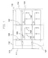
- FIG. 1 shows an example of circuit configuration in the AMLCD, which is referred to a so-called “Cs on Gate” AMLCD.
- the reference numeral 101 denotes a gate line for supplying a scanning signal
- the reference numeral 102 denotes a source line for supplying a voltage signal
- the reference numeral 103 denotes a thin film transistor (TFT) which is a switching element for applying a voltage to a liquid crystal
- the reference numeral 104 denotes a liquid crystal for switching transmission/non-transmission of light which is represented as a capacitance on an equivalent circuit
- the reference numeral 105 denotes a storage capacitance provided electrically in parallel with the liquid crystal 104 and serving to reduce the influence of a parasitic capacitance of a TFT
- the reference numeral 106 denotes a connecting portion for connecting an electrode on either side of the liquid crystal 104 to a common voltage
- the reference numeral 114 denotes a repair line to be used when the source line is open.
- a component which may be a TFT or an element of high resistance having linear or non linear characteristics may be provided between the gate terminal 107 and line 111 and between the source terminal 108 and line 112 to electrically isolate the gate terminal 107 and source terminal 108 during signal application and to electrically connect the gate terminal 107 and source terminal 108 when static electricity of high voltage invades.
- a TFT array is formed with such a configuration as shown in FIG. 1 as described above. After combined with a counter substrate on which a color filter is provided, a liquid crystal is injected therebetween and the outside of a region 115 shown in a dotted line in the drawing is generally cut out to form a liquid crystal display.
- repair line 114 for example, formed of the same material of the gate line to be a substitute of the source line is shown in FIG. 1, it does not need to be formed depending on circumstances.
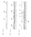
- FIG. 2( a ) is a partially enlarged plan view showing the TFT array of the AMLCD in FIG. 1 and FIG. 2( b ) is a sectional view taken along the line X-X in FIG. 2( a ). Since a terminal portion 303 is provided on the outside of the region of FIG. 2( a ), it is shown in only FIG. 2( b ).
- the reference numeral 211 denotes an insulative substrate
- the reference numeral 212 denotes a gate line formed of a conductive film
- the reference numeral 221 denotes a storage capacitance electrode
- the reference numeral 224 denotes a source line
- the reference numeral 225 denotes a drain electrode
- the reference numeral 214 denotes a pixel electrode formed of a transparent conductive layer.
- the gate line 212 also serves as the storage capacitance electrode 221 and the storage capacitance 105 is formed between the gate line 212 and the pixel electrode 214 .
- a first conductive film is formed on the first insulative substrate 211 .
- the first conductive film is formed of metal such as Cr, Al, Ti, Ta, Au, Ag, W, Mo, Mo—W or Cu, an alloy including either of or some of these metals as essential components, or a laminated layer of these metals and/or alloys, by a method such as sputtering, evaporation, CVD or printing.
- the gate line 212 and the storage capacitance electrode 221 are formed by photolithography and succeeding etching (FIG. 3( a )).
- an insulating film 216 comprising Si 3 N 4 is formed by a plasma CVD method, another suitable CVD method, sputtering, evaporation, coating or the like, and furthermore, an a ⁇ Si:H film 217 (a hydroxide amorphous silicon film) and an n+Si:H film 218 doped with an impurity such as phosphorus are continuously formed by a plasma CVD method, another suitable CVD method or sputtering.
- a second conductor layer 220 is formed of metal such as Cr, Al, Ti, Ta, Au, Ag, W, Mo, Mo—W or Cu, an alloy including either of or some of these metals as essential components or a laminated layer of these metals and/or alloys (FIG. 3( b )).
- a photosensitive organic resin which can be used as a photoresist.
- a photoresist pattern 219 is formed by exposure using a photomask (FIG. 3( c )). The shape of the photoresist pattern 219 will be described in detail.
- At least a part of a portion to be a pixel electrode later is set to be a region (region C) in which the photoresist is not formed.
- at least a portion to be a source electrode and a drain electrode later are set to be a region (region A) in which the photoresist has a great thickness.
- a portion in which the second conductor layer 220 and the n+Si:H film 218 are removed by etching to leave the a ⁇ Si:H film 217 for example, a channel portion 226 of the TFT is set to be a region (region B) in which the photoresist has a small thickness.
- the etching is carried out by using the photoresist pattern 219 .
- the second conductor layer 220 is etched by wet or dry etching or the like.
- the n+Si:H film 218 and the a ⁇ Si:H film 217 are etched.
- the conductor layer 220 , the n+Si:H film 218 and the a ⁇ Si:H film 217 in the region C are removed (FIG. 4( a )).
- ashing is carried out by using plasma capable of reducing the thickness of the photoresist, for example, an oxygen plasma, thereby scraping the photoresist to be removed from the region B (FIG. 4( b )).
- plasma capable of reducing the thickness of the photoresist for example, an oxygen plasma
- the thickness of the photoresist in the region A becomes smaller than an initial thickness, but the ashing is controlled to maintain such a thickness as to fully protect a portion which is not etched during etching at a subsequent step.
- the second conductor layer 220 exposed by removing the photoresist in the region B is removed by wet or dry etching or the like.
- n+Si:H film 218 in the region B is removed by the dry etching or the like and the photoresist is finally peeled to form a predetermined pattern (FIG. 4( c )).
- a protective film 222 is formed by an insulating film comprising Si 3 N 4 or SiO 2 , or their mixture and lamination.
- a photoresist pattern is provided by photolithography for forming a contact hole 233 in a gate terminal portion, a source terminal portion and a drain electrode portion, and subsequently, the contact hole 233 is formed by dry etching or wet etching using a CF 4 based gas. After the etching is completed, the photoresist is removed (FIG. 5( a )).
- a transparent conductive layer comprising a transparent conductive film such as ITO, SnO 2 or InZnO, a laminated layer thereof or a layer of mixture thereof is formed on the protective film 222 by a method such as sputtering, evaporation, coating, CVD, printing or a sol-gel method, and desirable patterns of the pixel electrode 214 , an upper pad 215 and the like are formed by photolithography and succeeding wet or dry etching or the like, so that a TFT array is formed (FIG. 5( b )).
- a transparent conductive film such as ITO, SnO 2 or InZnO
- an orientation film is formed on the TFT array and is opposed to a counter substrate having at least an orientation film and a common electrode on its surface, and a liquid crystal is injected therebetween to form an active matrix liquid crystal display, although not shown in the figures.
- the photoresist pattern 219 having the region A in which the photoresist has a great thickness, the region B in which the photoresist has a small thickness and the region C in which the photoresist is removed (the thickness is substantially zero) as shown in FIG. 3( c ), a so-called halftone mask is used as a photomask.
- the halftone mask is a photomask capable of carrying out intermediate exposure in addition to a binary process in which light illuminated from an exposing machine is transmitted or interrupted depending on the presence of a shielding film.
- the intermediate exposure can be obtained by alternately arranging a transmitting portion through which illuminated light is transmitted and a shielding portion through which illuminated light is not transmitted to thereby constitute a transmitting/shielding pattern and by sufficiently increasing the spatial frequency of the transmitting/shielding pattern than the pattern resolution of the exposing machine. Consequently, the transmitting/shielding pattern cannot be accurately exposed with the pattern resolution of the exposing machine, and the whole region of the photoresist below the transmitting/shielding pattern is exposed in an intermediate amount of exposure.
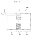
- a mask pattern SH 1 in FIG. 6 has a region A 1 for shielding the illuminated light of the exposing machine and a halftone region B 1 corresponding to the region B of the photoresist pattern 219 , and the halftone region B 1 is defined by transmitting/shielding pattern having a plurality of fine rectangular transmitting portions.
- the fine transmitting/shielding pattern cannot be drawn with the pattern resolution of the exposing machine. For this reason, the whole halftone region B 1 is exposed weakly.
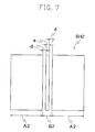
- a mask pattern SH 2 in FIG. 7 has a region A 2 for shielding the illuminated light of the exposing machine and a halftone region B 2 corresponding to the region B of the photoresist pattern 219 , and the halftone region B 2 is defined by a stripe-shaped transmitting/shielding pattern.
- the fine transmitting/shielding pattern cannot be drawn with the pattern resolution of the exposing machine. For this reason, the whole halftone region B 2 is exposed weakly.
- a photoresist pattern formed by using the halftone mask shown in FIG. 6 or 7 has such a thickness as shown in an explanatory view of FIG. 8.
- FIG. 8 shows the thickness of the photoresist in a shade of color, and a dark portion represents a region in which the photoresist has a great thickness and a light portion represents a region in which the photoresist has a small thickness.
- FIG. 9 shows the result obtained by carrying out a simulation using LILE (TRADE NAME; manufactured by Seiko Instruments) for the amount of exposure in the TFT array surface in the case in which the exposure is performed by using the halftone mask in FIG. 6 or FIG. 7. The result indicates a relative value, wherein the amount of exposure without the halftone mask is set to 1.
- the conditions of the simulation are as follows.
- Exposure wavelength 0.436 ⁇ m (g ray)
- the thickness of the photoresist in the region B is smaller than that of the photoresist in the region A.
- the thickness of the photoresist in the region B has a variation to show a poor uniformity.
- the photoresist in the region B is partially dissipated due to a fluctuation in the amount of exposure during exposure.
- the thickness of the photoresist in the region B is left too thickly so that a time required for removing the photoresist is increased at the time of ashing or the photoresist removing defect is partially caused. Consequently, yield is deteriorated or tact is increased.
- the amount of the exposure in the region B are varied.
- the photoresist is partially dissipated, the time required for removing the photoresist is increased and the photoresist removing defect is partially caused. Consequently, the yield is deteriorated and the tact is increased.
- the manufacturing cost of the TFT array is necessarily increased.
- the defect of the shape of the TFT is caused by the nonuniformity of the thickness of the photoresist.
- a variation in the length of a TFT channel portion is increased so that a display characteristic is deteriorated.
- the present invention has been made in consideration of the above-mentioned problems in the prior arts, and has an object to enhance the uniformity of the thickness of a photoresist in a halftone region and to implement high yield and low tact, and to suppress a variation in the channel length of a TFT to obtain display of high quality when forming the photoresist pattern by using a halftone mask.
- precision in the dimension of a photomask in a halftone region is set to 0.1 ⁇ m or less, desirably 0.05 ⁇ m or less, thereby enhancing the uniformity of the thickness of a film.
- the shape of the photomask on both ends of the halftone region is modified to increase the amount of exposure on both ends.
- a variation in a dimension between the photomasks is set to ⁇ 0.1 ⁇ m or less, desirably 0.05 ⁇ m or less, thereby causing the film thickness of the photoresist to be equal between the halftone regions.
- FIG. 1 is a diagram showing an example of the circuit configuration of an active matrix liquid crystal display
- FIG. 2 shows a TFT array of the active matrix liquid crystal display in FIG. 1, FIG. 2( a ) being a partially enlarged plan view and FIG. 2( b ) being a view showing an X-X section in FIG. 2( a );
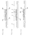
- FIG. 3 is a view illustrating a process for manufacturing the TFT array in FIG. 2;
- FIG. 4 is a view showing the process for manufacturing the TFT array in FIG. 2, illustrating a succeeding step to FIG. 3;
- FIG. 5 is a view showing the process for manufacturing the TFT array in FIG. 2, illustrating a succeeding step to FIG. 4;
- FIG. 6 is a diagram showing an example of a halftone mask pattern
- FIG. 7 is a diagram showing another example of the halftone mask pattern
- FIG. 8 is a typical view illustrating the distribution of a film thickness of a photoresist
- FIG. 9 is a view representing a result obtained by a simulation for the amount of exposure in a TFT array surface
- FIG. 10 is a view illustrating a process for manufacturing a TFT array according to the present invention.
- FIG. 11 is a view showing the process for manufacturing the TFT array according to the present invention, illustrating a succeeding step to FIG. 10;
- FIG. 12 is a view showing the process for manufacturing the TFT array according to the present invention, illustrating a succeeding step to FIG. 11;
- FIG. 13 is a chart showing the relationship between the dimensional error of a transmitting/shielding pattern and the film thickness of a photoresist
- FIG. 14 is a view showing an example of a photomask pattern according to the present embodiment.
- FIG. 15 is a view showing another example of the photomask pattern according to the present embodiment.
- FIG. 16 is a typical view illustrating the distribution of the film thickness of a photoresist pattern in a manufacturing method according to the present invention.
- FIG. 17 is a view representing a result obtained by a simulation for the amount of exposure in a TFT array surface in the manufacturing method according to the present invention.
- FIG. 18 is a diagram illustrating the structure of a circuit in a liquid crystal display having a common line structure
- FIG. 19 shows the TFT array of the active matrix liquid crystal display in FIG. 18, FIG. 19( a ) being a partially enlarged plan view and FIG. 19( b ) being a view showing a Y-Y section in FIG. 19( a ); and
- FIG. 20 is a view illustrating a TFT array of a liquid crystal display of In-Plane-switching mode.
- a first conductive film is formed on a first insulating substrate 211 .
- the first conductive film is formed of metal such as Cr, Al, Ti, Ta, Au, Ag, W, Mo, Mo—W or Cu, an alloy containing either of or some of these metals as essential components, or a laminated layer of these metals and/or alloys, by a method such as sputtering, evaporation, CVD or printing.
- a gate line 212 , a storage capacitance electrode 221 and the like are formed by photolithography and succeeding etching and the like (FIG. 10( a )).
- an insulating film 216 comprising Si 3 N 4 , a substance which is slightly deviated from a stoichiometric composition or a composition thereof is formed by a plasma CVD method, another suitable CVD method, sputtering, evaporation, coating or the like.
- an a ⁇ Si:H film (a hydroxide amorphous silicon film) 217 to be used as a semiconductor layer for a channel which is not doped with an impurity or is intentionally doped with the impurity with an impurity concentration of approximately 50 ppm or less, or a dopant concentration such that a dark current does not exceed 50 pA on actual use voltage conditions.
- a second conductive film 220 is formed of metal such as Cr, Al, Ti, Ta, Au, Ag, W, Mo, Mo—W or Cu, an alloy containing either of or some of these metals as essential components or a laminated layer of these metals and/or alloys (FIG. 10( b )).
- the photoresist pattern 219 has the following configuration.
- a portion in which the conductive layer 220 , the n+Si:H film 218 and the a ⁇ Si:H film 217 should be removed for example, at least a part of a portion to be a pixel electrode later is set to be a region in which the photoresist is not formed (region C). Moreover, at least a portion to be a source electrode and a drain electrode later is set to be a region in which the photoresist has a great thickness (region A).
- a TFT channel portion 226 is set to be a region in which the photoresist has a small thickness (region B).
- At least a part of a portion on the gate line 212 between adjacent source lines should be set to be the region C, so that the a ⁇ Si:H film 217 should be removed in addition to the conductive layer 220 and the n+Si:H film 218 , thereby electrically isolates adjacent source lines (i.e. semiconductor layers between adjacent source lines are not continuously provided).
- a halftone mask is used.
- the halftone mask will be described below. While a positive photoresist is used in the present embodiment, a photoresist pattern can be basically formed by the same method with a negative photoresist.
- a portion in which the region C having no photoresist is to be formed is set such that the photomask is brought into an almost transparent, so that light is transmitted sufficiently and the photoresist is exposed with a sufficient amount of light so as not to cause the photoresist to remain at time of development. As a result, the photoresist is completely removed at time of the development so that the region C having no photoresist is formed.
- a transmitting portion through which the exposing light is transmitted and a shielding portion through which the exposing light is not transmitted are alternately provided on the photomask, thereby defining a transmitting/shielding pattern.
- the region through which the exposing light is transmitted By providing the region through which the exposing light is transmitted, the region through which the exposing light is not transmitted, and the transmitting/shielding pattern on the photomask, it is possible to form a photoresist pattern including three regions of the region C, the region A and the region B which have different thicknesses.
- the amount of exposure or the amount of light is represented by multiplying light intensity by time.
- the thickness of the photoresist in the region B has a poor uniformity. Furthermore, the photoresist in the region B is partially dissipated due to a fluctuation in the amount of exposure at time of the exposure. On the contrary, the photoresist is left thickly so that a time required for removing the photoresist is increased at time of ashing or photoresist removing defects are partially caused.
- the amount of the exposure in the region B are varied so that the photoresist is partially dissipated, the time required for removing the photoresist is increased and the photoresist removing defects are partially caused.
- One of the causes of the nonuniformity in the thickness of the photoresist includes dimensional precision in the transmitting/shielding pattern.
- the transmitting/shielding pattern is defined by a rectangular transmitting portion having a length a and a width c and a shielding portion having a length b and a width e which are alternately provided.
- FIG. 13 shows the thickness of the photoresist in the central part of the region B in the case in which the dimension has an error in the transmitting/shielding pattern.
- the dimensional error of the mask pattern is caused by overetching/underething when the mask is to be patterned. Therefore, in the case in which the dimension a has an error, it can be supposed that a dimension (a+b) is almost constant. In FIG. 13, accordingly, it is assumed that the dimension (a+b) is constant.
- the thickness of the photoresist in the region B is almost half (0.5) of the thickness of the region A.
- the thickness of the photoresist in the region B is 1.0, that is, is equal to that in the region A or the thickness of the photoresist is 0, that is, is equal to that in the region C.
- the dimensional error of a conventional photomask for forming a general TFT array is more than ⁇ 0.1 ⁇ m.
- the thickness of the photoresist in the region B is sometimes 1.0, that is, is equal to that in the region A or the thickness of the photoresist is sometimes 0, that is, is equal to that in the region C. For this reason, yield is deteriorated when forming the region B.
- At least the dimensional error of the transmitting/shielding pattern of the photomask is set to be ⁇ 0.1 ⁇ m or less. Consequently, the photoresist in the region B can be prevented from being dissipated partially. On the contrary, the photoresist can be prevented from being left thickly to increase the time required for removing the photoresist at time of the ashing or the photoresist removing defects can be prevented from being generated partially. Thus, it is possible to enhance the yield and to shorten tact.
- the dimensional error of the transmitting/shielding pattern to be ⁇ 0.05 ⁇ m or less, furthermore, the uniformity of the thickness of the photoresist in the region B can be enhanced still more. Consequently, even in the case in which the amount of exposure at time of the exposure and the amount of resist removal in the region B at a subsequent step are varied, the partial dissipation and removing defects of the photoresist can be decreased and the yield can be enhanced considerably.
- a plurality of photomasks are selected such that a variation in the dimension of the transmitting/shielding pattern of the photomask is 0.1 ⁇ m or less, and these masks are used to carry out the exposure. Consequently, it is possible to suppress a variation in the thickness in a plurality of regions B, and the photoresist in the region B can be prevented from being dissipated partially. To the contrary, the photoresist removing defects can be prevented from being generated partially.
- the photoresist pattern 219 is formed by using such a photomask, and the second conductive layer 220 is first etched by wet or dry etching or the like, thereby forming a source line, a source electrode and a drain electrode. Subsequently, the n+Si:H film 218 and the a ⁇ Si:H film 217 are subjected to etching.
- the etching is carried out by a gas containing HCl as an essential component, a gas containing CF 4 as an essential component, a mixed gas of CF 4 and O 2 , a gas containing SF 6 as an essential component or the like, for example.
- the n+Si:H film 218 and the a ⁇ Si:H film 217 are removed from a portion to be at least a part of a pixel electrode to transmit light therethrough.
- a terminal portion 303 to be connected to a TCP or the like in order to input a signal from the outside to a gate line or a portion to be short-circuited with a source line directly or through a TFT or a resistor in order to prevent static electricity moreover, the n+Si:H film 218 and the a ⁇ Si:H film 217 may be removed at this step (FIG. 11( a )).
- the ashing is carried out by using a plasma capable of reducing the thickness of the photoresist, for example, an oxygen plasma, thereby scraping the photoresist to be removed from the region B (FIG. 11( b )).
- a plasma capable of reducing the thickness of the photoresist for example, an oxygen plasma
- the thickness of the photoresist in the region A becomes smaller than an initial thickness but sufficient thickness is held such that a portion which is not etched at a succeeding etching step can be protected sufficiently.
- the photoresist in the region B may be scraped by the dry etching for removing the n+Si:H film 218 and the a ⁇ Si:H film 217 .
- the uniformity of the thickness of the photoresist in the region B exposed by the photomask pattern is excellent. Therefore, it is possible to reduce the residual photoresist, to enhance the yield of the photoresist removal and to shorten the photoresist removing tact. Moreover, the shape of the photoresist in the region A can be enhanced after the photoresist in the region B is removed and the second conductive layer 220 of the TFT channel portion 226 can be accurately removed. Accordingly, the channel length of the TFT can particularly be controlled easily and quality of display can be enhanced.
- a mask pattern for forming the region B of the TFT is made equivalent to those for forming the region B of the TFT in the display portion so that the thickness of the resist can be equal and the yield can be thereby enhanced.
- a portion exposed by removing the photoresist in the region B i.e. at least the second conductive layer 220 of the TFT channel portion 226 , is etched by wet or dry etching or the like.
- n+Si:H film 218 in the TFT channel portion 226 is removed by the dry etching or the like and the photoresist 219 is finally peeled so that a predetermined pattern is obtained (FIG. 11( c )).
- a passivation film 222 is formed by an insulating film comprising Si 3 N 4 or SiO 2 , or their mixture and lamination.
- a photoresist pattern for forming a contact hole 233 is provided by photolithography in a gate terminal portion, a source terminal portion and a drain electrode portion, and subsequently, the contact hole 233 is formed by dry etching using a CF 4 based gas or wet etching. After the etching is completed, the photoresist is removed (FIG. 12( a )).
- a transparent conductive layer comprising a transparent conductive film such as ITO, SnO 2 or InZnO, a laminated layer thereof or a layer comprising a mixture thereof is formed on the passivation film 222 by a method such as sputtering, evaporation, coating, CVD, printing or a sol-gel method, and a predetermined pattern of the pixel electrode 214 , an upper pad 215 and the like are formed by photolithography and succeeding wet or dry etching or the like so that a TFT array is formed (FIG. 12( b )).
- a transparent conductive layer comprising a transparent conductive film such as ITO, SnO 2 or InZnO, a laminated layer thereof or a layer comprising a mixture thereof is formed on the passivation film 222 by a method such as sputtering, evaporation, coating, CVD, printing or a sol-gel method, and a predetermined pattern of the pixel electrode 214 , an upper pad
- an orientation film is formed on the TFT array and is opposed to a counter substrate having at least an orientation film and a common electrode on its surface, and a liquid crystal is injected therebetween to form an active matrix liquid crystal display, which is not shown.
- the uniformity of the thickness in the region B has been enhanced such that the dimensional error of the transmitting/shielding pattern of the photomask is ⁇ 0.1 ⁇ m or less, desirably 0.05 ⁇ m or less.
- a plurality of photomasks are selected such that a variation in the dimension of the transmitting/shielding pattern is ⁇ 0.1 ⁇ m or less, desirably 0.05 ⁇ m or less.
- the present embodiment has an object to suppress a variation in the thickness of the photoresist in the region B by modifying a transmitting/shielding pattern itself.
- FIG. 14 shows a photomask pattern SH 3 according to the present embodiment.
- the mask pattern SH 3 in FIG. 14 has a region A 3 for shielding the illuminated light of the exposing machine and a halftone region B 3 corresponding to a region B of a photoresist pattern 219 , and is similar to the conventional mask pattern SH 1 shown in FIG. 6 in that the halftone region B 3 is defined by a transmitting/shielding pattern in which a plurality of rectangular transmitting portions and shielding portions are arranged alternately.
- the conventional mask pattern SH 1 there is a problem in that the amount of exposure is particularly insufficient in the vicinity of the end of the region B and the thickness of the photoresist is increased as shown in FIGS. 8 and 9.
- the area of a transmitting portion PE 1 positioned on both ends in the transmitting portions is set to be larger than the areas of other transmitting portions.
- the transmitting portion PE 1 on both ends has a length a 1 and a width c 1 and an adjacent transmitting portion PE 2 has a length a 2 and a width c 2 .
- the areas of the transmitting portions are set to PE 1 >PE 2 so that the amount of the exposure on both ends in the region B of the photomask pattern can be increased.
- a photomask can be formed within a range of manufacturing precision in a photomask pattern and the uniformity of the amount of the exposure in the whole region B can be enhanced.
- a 1 (a 2 +0.25 ⁇ m) can be set.
- the width c 1 of the transmitting portion PE 1 and the width c 2 of the transmitting portion PE 2 have a relationship of c 1 >c 2
- the areas of the transmitting portions are set to PE 1 >PE 2 so that the amount of the exposure on both ends in the region B can be increased.
- a photomask can be formed within a range of manufacturing precision in a photomask pattern and the uniformity of the amount of the exposure in the whole region B can be enhanced.
- c 1 (c 2 +0.6 ⁇ m) can be set.
- a distance b 1 between an end side of the photomask pattern and the transmitting portion PE 1 and a length b 2 of the shielding portion provided between the transmitting portion PE 1 and the transmitting portion PE 2 are set to b 2 >b 1 , the rate of occupation of the transmitting portion in the vicinity of the end of the region B is increased so that the amount of the exposure can be increased.
- b 1 +0.1 ⁇ m) ⁇ b 2 ⁇ (b 1 +0.5 ⁇ m) is set, a photomask can be formed within a range of manufacturing precision in a photomask pattern and the uniformity of the amount of the exposure in the whole region B can be enhanced.
- b 2 (b 1 +0.25 ⁇ m) can be set.
- the shape of the mask pattern is set such that the rate of the transmitting portion is increased when the end of the region B is closer. Consequently, the amount of the exposure can be increased in the vicinity of the end of the region B so that the uniformity of the amount of the exposure in the whole region B can be enhanced.
- a photomask pattern for making the amount of the exposure in the region B uniform includes the three patterns described above. By using one of the three patterns, the thickness of the photoresist can be made uniform. By using two or more in combination, the uniformity can be enhanced still more.
- the thickness of the photoresist to be formed can be set to region A>region B>region C and the uniformity of the thickness of the exposed photoresist can be enhanced.
- the uniformity of the thickness of the photoresist in the region B formed on the same substrate can be enhanced by using a halftone mask in which the dimensions a 1 , a 2 , b 1 , b 2 , c 1 and c 2 of the mask pattern are almost equal.
- the modification of the transmitting/shielding patterns of the photomasks can also be applied to the formation of an element to be formed by using a TFT for protection against static electricity in addition to the region B of the TFT for each pixel.
- the uniformity of the thickness of the photoresist can be enhanced.
- each region B of the element and the TFT for each pixel formed in the same substrate is set to be almost equal so that uniformity of photoresist removal in the region B can be enhanced, and the photoresist can be prevented from being dissipated partially and the partial removing defects of the photoresist can be prevented so that yield can be enhanced.
- the TFT for each pixel and the like formed in the same substrate furthermore, the uniformity of the thickness of the photoresist in the region B formed in the same substrate can be enhanced by using the halftone mask in which the dimensions a 1 , a 2 , b 1 , b 2 , c 1 and c 2 of the mask pattern are almost equal.
- a transmitting/shielding pattern for forming the region B has the shape of a stripe in which a transmitting portion having a predetermined width d over the whole length of the photomask and a shielding portion having a predetermined width e over the whole length of the photomask are provided alternately.
- the thickness of a photoresist in the central part of the region B is obtained as shown in FIG. 13. It is assumed that a width (d+e) is constant. In the case in which the dimension of the width d has no error as designed, the thickness of the photoresist in the region B is almost half (0.5) of the thickness in the region A.
- the thickness of the photoresist in the region B is 1.0, that is, is equal to that in the region A or the thickness of the photoresist is 0, that is, is equal to that in the region C.
- the dimensional error of the conventional photomask for forming a general TFT array is more than ⁇ 0.1 ⁇ m. Therefore, the thickness of the photoresist in the region B is sometimes 1.0, that is, is equal to that in the region A or the thickness of the photoresist is sometimes 0, that is, is equal to that in the region C due to the dimensional error of the transmitting/shielding pattern. For this reason, yield is deteriorated when forming the region B.
- the photoresist in the region B can be prevented from being dissipated partially.
- the photoresist can be prevented from being left thickly to increase a time required for removing the photoresist at time of ashing, and the photoresist removing defects can be prevented from being caused partially. Consequently, the yield can be enhanced and tact can be shortened.
- the dimensional error of the transmitting/shielding pattern By setting the dimensional error of the transmitting/shielding pattern to be ⁇ 0.05 ⁇ m or less, furthermore, the uniformity of the thickness of the photoresist in the region B can be enhanced still more. Also in the case in which the amount of exposure at time of the exposure or the amount of resist removal in the region B at a subsequent step is varied, the partial dissipation and removing defects of the photoresist are not caused so that the yield can be enhanced considerably.
- a plurality of photomasks are preferably selected such that a variation in the dimension of a width (d+e) in a pair of adjacent transmitting and shielding portions in the transmitting/shielding pattern of the photomask is 0.1 ⁇ m or less, and these photomasks are used to carry out the exposure. Consequently, it is possible to suppress a variation in the thickness in a plurality of regions B, and the photoresist in the region B can be prevented from being dissipated partially. To the contrary, the photoresist removing defects can be prevented from being generated partially.
- the uniformity of the thickness in the region B has been enhanced such that the dimensional error of the transmitting/shielding pattern of the photomask is ⁇ 0.1 ⁇ m or less, desirably 0.05 ⁇ m or less.
- a plurality of photomasks are selected such that a variation in the dimension of the transmitting/shielding pattern is ⁇ 0.1 ⁇ m or less, desirably 0.05 ⁇ m or less.
- the present embodiment has an object to suppress a variation in the thickness of the photoresist in the region B by modifying a transmitting/shielding pattern.
- FIG. 15 shows a photomask pattern SH 4 according to the present embodiment.
- the mask pattern SH 4 in FIG. 15 is similar to the conventional mask pattern SH 2 shown in FIG. 7 in that it has a region A 4 for shielding the illuminated light of the exposing machine and a halftone region B 4 corresponding to a region B of the photoresist pattern 219 and the halftone region B 4 has a stripe-shaped transmitting/shielding pattern in which a transmitting portion having a predetermined width d and a shielding portion having a predetermined width e are alternately provided over the whole length of the photomask.
- the conventional mask pattern SH 2 there is a problem in that the amount of exposure is particularly insufficient in the vicinity of the end of the region B and the thickness of the photoresist is increased as shown in FIGS. 8 and 9.
- projections PR 1 , PR 2 , PR 3 and PR 4 are provided as correction patterns on both ends of the stripe-shaped transmitting portion to increase the amount of the exposure in both ends of the region B.
- the amount of protrusion of the projections PR 1 , PR 2 , PR 3 and PR 4 from the transmitting portion is represented by f
- a width is represented by g
- a distance from each projection to the end of the photomask is represented by h.
- the transmitting/shielding pattern is formed to set d ⁇ e, f>0.1 ⁇ m, g>0.5 ⁇ m and h>0.5 ⁇ m.
- a photomask can be formed within a range of manufacturing precision in a photomask pattern and the uniformity of the amount of the exposure in the whole region B can be enhanced.
- d 1.1 ⁇ m
- e 1.4 ⁇ m
- f 0.3 ⁇ m
- g 1.8 ⁇ m
- the uniformity of the thickness of the photoresist in the region B can be more enhanced. Consequently, the yield of the photoresist removal can be enhanced and the tact of the photoresist removal can be shortened. Moreover, the uniformity of the thickness of the photoresist in the region B can be enhanced. Consequently, the shape of the second conductive film in the region A can be well controlled after the photoresist in the region B is removed, so that the channel length of a TFT can be easily suppressed and quality of display can be enhanced.
- a photoresist pattern formed by using the halftone mask shown in FIG. 15 has such a thickness as shown in an explanatory view of FIG. 16.
- FIG. 16 shows the thickness of the photoresist in a shade of color, and a dark portion represents a region in which the photoresist has a great thickness and a light portion represents a region in which the photoresist has a small thickness.
- FIG. 17 shows the result obtained by carrying out a simulation using LILE (TRADE NAME; manufactured by Seiko Instruments) for the amount of exposure in the TFT array surface in the case in which the exposure is performed by using the halftone mask in FIG. 15. The result indicates a relative value, wherein the amount of exposure without the halftone mask is set to 1.
- the conditions of the simulation are as follows.
- Exposure wavelength 0.436 ⁇ m (g ray)
- a TFT array having the common storage line structure is shown in a circuit diagram of FIG. 18.
- a storage capacitance 105 is connected to a common line 120 .
- each common line 120 is connected to a common line lead 121 .
- a common voltage is applied from the outside through a common line terminal 123 connected to the common line lead. Since the functions of other components and the reference numerals in the drawings are the same as those in FIG. 1, description will be omitted.
- the TFT array has a planar and sectional structure shown in FIG. 19, for example.
- a common line 120 (the storage capacitance electrode 221 in FIG. 19) arranged in parallel with the gate line and a common line lead 121 arranged in perpendicular to the gate line 101 (the gate line 212 in FIG. 19) to connect common lines 120 thereto are required.
- the common line 120 (the storage capacitance electrode 221 ) should be formed of the same material as the material of the gate line 101 (the gate line 212 ) at the same time, that is, should be formed of a first conductive film
- the common line lead 121 is formed of the material of a different layer from the gate line 101 , for example, a second metal layer which is the same as the source line in at least a portion 124 (see FIG. 18) intersecting the gate line 101 .
- Portions in the common line lead 121 other than the portion intersecting the gate line 101 may be formed of the same material as that of the gate line 101 at the same time, that is, the first conductive film.
- FIG. 20 is a plan view showing a TFT array according to the present embodiment.
- the reference numerals in the drawing are the same as those in FIGS. 2 and 19.
- a common electrode 228 is also provided in the TFT array and a liquid crystal is driven by a potential difference between a pixel electrode 214 and a common electrode 228 .
- a gate line 212 and a common line 227 are formed of the same layer at the step shown in FIG. 10( a ) and a source line 224 and a drain electrode 220 are formed of the same layer at the step shown in FIG. 11( c ). Then, the pixel electrode 214 and the common electrode 228 are formed of the same layer at the step shown in FIG. 12( b ). The pixel electrode 214 and the common electrode 228 are connected to the drain electrode 220 and the common line 227 through a contact hole 233 , respectively.
- the gate line 212 and the common line 227 are formed of the same layer at the step shown in FIG. 10( a ) and the source line 224 , the pixel electrode 214 and the common electrode 228 can be then formed of the same layer at the step shown in FIG. 11( c ).
- the semiconductor layers comprise a ⁇ Si in EMBODIMENT 1 to EMBODIMENT 6, Poly ⁇ Si is also applicable.
- dimensional precision in a photomask particularly, dimensional precision in a transmitting/shielding pattern for carrying out halftone exposure is enhanced and the configuration of the transmitting/shielding pattern is devised in order to control the thickness of a photoresist for forming a TFT channel portion. Consequently, it is possible to enhance the uniformity of the thickness of the photoresist and the reproducibility in film thickness formation, and yield can be enhanced and a cost can be reduced. Moreover, since variation in the channel length of a TFT can be suppressed, an enhancement in quality of display can be implemented.
Landscapes
- Physics & Mathematics (AREA)
- General Physics & Mathematics (AREA)
- Liquid Crystal (AREA)
- Thin Film Transistor (AREA)
- Preparing Plates And Mask In Photomechanical Process (AREA)
- Exposure And Positioning Against Photoresist Photosensitive Materials (AREA)
Abstract
Description
- The present invention relates to a method of manufacturing a TFT array of a liquid crystal display, and more particularly to a photomask to be used for exposing a photoresist to form a photoresist pattern.
- In a liquid crystal display, an electric field is applied to a liquid crystal held between opposed substrates, for carrying out display. A liquid crystal display has a lighter weight, smaller power consumption and greater portability than those of a CRT. In particular, an active matrix liquid crystal display (AMLCD), in which a switching element such as a thin film transistor (TFT) is provided on a substrate to control an electric field to be applied to a liquid crystal, is very excellent in quality of display and has recently been applied to wide uses.
- Referring to FIGS. 1 and 2, the active matrix liquid crystal display (AMLCD) will be described. FIG. 1 shows an example of circuit configuration in the AMLCD, which is referred to a so-called “Cs on Gate” AMLCD. The
reference numeral 101 denotes a gate line for supplying a scanning signal, thereference numeral 102 denotes a source line for supplying a voltage signal, thereference numeral 103 denotes a thin film transistor (TFT) which is a switching element for applying a voltage to a liquid crystal, thereference numeral 104 denotes a liquid crystal for switching transmission/non-transmission of light which is represented as a capacitance on an equivalent circuit, thereference numeral 105 denotes a storage capacitance provided electrically in parallel with theliquid crystal 104 and serving to reduce the influence of a parasitic capacitance of a TFT, thereference numeral 106 denotes a connecting portion for connecting an electrode on either side of theliquid crystal 104 to a common voltage, thereference numeral 107 denotes a gate terminal for connecting an external circuit on the gate side to thegate line 101 through a TCP or the like, thereference numeral 108 denotes a source terminal for connecting an external circuit on the source side to thesource line 102 through the TCP or the like, thereference numeral 111 denotes a line connected to thegate lines 101, thereference numeral 112 denotes a line connected to thesource lines 102, and thereference numeral 113 denotes a connection for connecting theline 111 to theline 112. Thereference numeral 114 denotes a repair line to be used when the source line is open. Although not shown in FIG. 1, a component which may be a TFT or an element of high resistance having linear or non linear characteristics may be provided between thegate terminal 107 andline 111 and between thesource terminal 108 andline 112 to electrically isolate thegate terminal 107 andsource terminal 108 during signal application and to electrically connect thegate terminal 107 andsource terminal 108 when static electricity of high voltage invades. In many cases, a TFT array is formed with such a configuration as shown in FIG. 1 as described above. After combined with a counter substrate on which a color filter is provided, a liquid crystal is injected therebetween and the outside of aregion 115 shown in a dotted line in the drawing is generally cut out to form a liquid crystal display. - While the
repair line 114, for example, formed of the same material of the gate line to be a substitute of the source line is shown in FIG. 1, it does not need to be formed depending on circumstances. - FIG. 2( a) is a partially enlarged plan view showing the TFT array of the AMLCD in FIG. 1 and FIG. 2(b) is a sectional view taken along the line X-X in FIG. 2(a). Since a
terminal portion 303 is provided on the outside of the region of FIG. 2(a), it is shown in only FIG. 2(b). - In FIG. 2, the
reference numeral 211 denotes an insulative substrate, thereference numeral 212 denotes a gate line formed of a conductive film, thereference numeral 221 denotes a storage capacitance electrode, thereference numeral 224 denotes a source line, thereference numeral 225 denotes a drain electrode, and thereference numeral 214 denotes a pixel electrode formed of a transparent conductive layer. In the Cs on Gate AMLCD, thegate line 212 also serves as thestorage capacitance electrode 221 and thestorage capacitance 105 is formed between thegate line 212 and thepixel electrode 214. - A process for manufacturing the TFT array in FIG. 2 will be described with reference to FIGS. 3, 4 and 5.
- First of all, a first conductive film is formed on the first
insulative substrate 211. The first conductive film is formed of metal such as Cr, Al, Ti, Ta, Au, Ag, W, Mo, Mo—W or Cu, an alloy including either of or some of these metals as essential components, or a laminated layer of these metals and/or alloys, by a method such as sputtering, evaporation, CVD or printing. Subsequently, thegate line 212 and thestorage capacitance electrode 221 are formed by photolithography and succeeding etching (FIG. 3(a)). - Then, an
insulating film 216 comprising Si3N4 is formed by a plasma CVD method, another suitable CVD method, sputtering, evaporation, coating or the like, and furthermore, an a−Si:H film 217 (a hydroxide amorphous silicon film) and an n+Si:H film 218 doped with an impurity such as phosphorus are continuously formed by a plasma CVD method, another suitable CVD method or sputtering. - Next, a
second conductor layer 220 is formed of metal such as Cr, Al, Ti, Ta, Au, Ag, W, Mo, Mo—W or Cu, an alloy including either of or some of these metals as essential components or a laminated layer of these metals and/or alloys (FIG. 3(b)). - Subsequently, the whole surface is first coated with a photosensitive organic resin which can be used as a photoresist. Then, a
photoresist pattern 219 is formed by exposure using a photomask (FIG. 3(c)). The shape of thephotoresist pattern 219 will be described in detail. - First of all, at least a part of a portion to be a pixel electrode later is set to be a region (region C) in which the photoresist is not formed. Moreover, at least a portion to be a source electrode and a drain electrode later are set to be a region (region A) in which the photoresist has a great thickness. Moreover, a portion in which the
second conductor layer 220 and the n+Si:H film 218 are removed by etching to leave the a−Si:H film 217, for example, achannel portion 226 of the TFT is set to be a region (region B) in which the photoresist has a small thickness. - Subsequently, the etching is carried out by using the
photoresist pattern 219. First of all, thesecond conductor layer 220 is etched by wet or dry etching or the like. Then, the n+Si:H film 218 and the a−Si:H film 217 are etched. Theconductor layer 220, the n+Si:H film 218 and the a−Si:H film 217 in the region C are removed (FIG. 4(a)). - Thereafter, ashing is carried out by using plasma capable of reducing the thickness of the photoresist, for example, an oxygen plasma, thereby scraping the photoresist to be removed from the region B (FIG. 4( b)). At this time, the thickness of the photoresist in the region A becomes smaller than an initial thickness, but the ashing is controlled to maintain such a thickness as to fully protect a portion which is not etched during etching at a subsequent step.
- Subsequently, the
second conductor layer 220 exposed by removing the photoresist in the region B is removed by wet or dry etching or the like. - Then, at least the n+Si:
H film 218 in the region B is removed by the dry etching or the like and the photoresist is finally peeled to form a predetermined pattern (FIG. 4(c)). - Thereafter, a
protective film 222 is formed by an insulating film comprising Si3N4 or SiO2, or their mixture and lamination. A photoresist pattern is provided by photolithography for forming acontact hole 233 in a gate terminal portion, a source terminal portion and a drain electrode portion, and subsequently, thecontact hole 233 is formed by dry etching or wet etching using a CF4 based gas. After the etching is completed, the photoresist is removed (FIG. 5(a)). - Next, a transparent conductive layer comprising a transparent conductive film such as ITO, SnO 2 or InZnO, a laminated layer thereof or a layer of mixture thereof is formed on the
protective film 222 by a method such as sputtering, evaporation, coating, CVD, printing or a sol-gel method, and desirable patterns of thepixel electrode 214, anupper pad 215 and the like are formed by photolithography and succeeding wet or dry etching or the like, so that a TFT array is formed (FIG. 5(b)). - Furthermore, an orientation film is formed on the TFT array and is opposed to a counter substrate having at least an orientation film and a common electrode on its surface, and a liquid crystal is injected therebetween to form an active matrix liquid crystal display, although not shown in the figures. Through the above-mentioned steps, the TFT array and a liquid crystal display using the TFT array are formed.
- In order to form the
photoresist pattern 219 having the region A in which the photoresist has a great thickness, the region B in which the photoresist has a small thickness and the region C in which the photoresist is removed (the thickness is substantially zero) as shown in FIG. 3(c), a so-called halftone mask is used as a photomask. - The halftone mask is a photomask capable of carrying out intermediate exposure in addition to a binary process in which light illuminated from an exposing machine is transmitted or interrupted depending on the presence of a shielding film. The intermediate exposure can be obtained by alternately arranging a transmitting portion through which illuminated light is transmitted and a shielding portion through which illuminated light is not transmitted to thereby constitute a transmitting/shielding pattern and by sufficiently increasing the spatial frequency of the transmitting/shielding pattern than the pattern resolution of the exposing machine. Consequently, the transmitting/shielding pattern cannot be accurately exposed with the pattern resolution of the exposing machine, and the whole region of the photoresist below the transmitting/shielding pattern is exposed in an intermediate amount of exposure.
- An actual halftone mask pattern is illustrated in FIGS. 6 and 7. A mask pattern SH 1 in FIG. 6 has a region A1 for shielding the illuminated light of the exposing machine and a halftone region B1 corresponding to the region B of the
photoresist pattern 219, and the halftone region B1 is defined by transmitting/shielding pattern having a plurality of fine rectangular transmitting portions. The fine transmitting/shielding pattern cannot be drawn with the pattern resolution of the exposing machine. For this reason, the whole halftone region B1 is exposed weakly. - A mask pattern SH 2 in FIG. 7 has a region A2 for shielding the illuminated light of the exposing machine and a halftone region B2 corresponding to the region B of the
photoresist pattern 219, and the halftone region B2 is defined by a stripe-shaped transmitting/shielding pattern. As a matter of course, the fine transmitting/shielding pattern cannot be drawn with the pattern resolution of the exposing machine. For this reason, the whole halftone region B2 is exposed weakly. - A photoresist pattern formed by using the halftone mask shown in FIG. 6 or 7 has such a thickness as shown in an explanatory view of FIG. 8. FIG. 8 shows the thickness of the photoresist in a shade of color, and a dark portion represents a region in which the photoresist has a great thickness and a light portion represents a region in which the photoresist has a small thickness. Moreover, FIG. 9 shows the result obtained by carrying out a simulation using LILE (TRADE NAME; manufactured by Seiko Instruments) for the amount of exposure in the TFT array surface in the case in which the exposure is performed by using the halftone mask in FIG. 6 or FIG. 7. The result indicates a relative value, wherein the amount of exposure without the halftone mask is set to 1. Moreover, the conditions of the simulation are as follows.
- Simulation condition:
- Exposure wavelength=0.436 μm (g ray)
- Numerical aperture (NA) of projection lens of stepper=0.1
- Illumination system coherency (σ)=0.5
- As is apparent from FIGS. 8 and 9, the thickness of the photoresist in the region B (halftone regions B 1 or B2) is smaller than that of the photoresist in the region A. However, the thickness of the photoresist in the region B has a variation to show a poor uniformity.
- Accordingly, the photoresist in the region B is partially dissipated due to a fluctuation in the amount of exposure during exposure. To the contrary, the thickness of the photoresist in the region B is left too thickly so that a time required for removing the photoresist is increased at the time of ashing or the photoresist removing defect is partially caused. Consequently, yield is deteriorated or tact is increased.
- Moreover, in the case in which a plurality of halftone masks are used for one substrate to carry out the exposure, the amount of the exposure in the region B are varied. As a matter of course, the photoresist is partially dissipated, the time required for removing the photoresist is increased and the photoresist removing defect is partially caused. Consequently, the yield is deteriorated and the tact is increased.
- For these reasons, the manufacturing cost of the TFT array is necessarily increased. Moreover, the defect of the shape of the TFT is caused by the nonuniformity of the thickness of the photoresist. In particular, a variation in the length of a TFT channel portion is increased so that a display characteristic is deteriorated.
- The present invention has been made in consideration of the above-mentioned problems in the prior arts, and has an object to enhance the uniformity of the thickness of a photoresist in a halftone region and to implement high yield and low tact, and to suppress a variation in the channel length of a TFT to obtain display of high quality when forming the photoresist pattern by using a halftone mask.
- In order to solve the above-mentioned problems, in the present invention, precision in the dimension of a photomask in a halftone region is set to 0.1 μm or less, desirably 0.05 μm or less, thereby enhancing the uniformity of the thickness of a film.
- Moreover, the shape of the photomask on both ends of the halftone region is modified to increase the amount of exposure on both ends.
- Furthermore, in the case in which a plurality of halftone masks are used for one substrate to carry out the exposure, a variation in a dimension between the photomasks is set to ±0.1 μm or less, desirably 0.05 μm or less, thereby causing the film thickness of the photoresist to be equal between the halftone regions. dr
- FIG. 1 is a diagram showing an example of the circuit configuration of an active matrix liquid crystal display;
- FIG. 2 shows a TFT array of the active matrix liquid crystal display in FIG. 1, FIG. 2( a) being a partially enlarged plan view and FIG. 2(b) being a view showing an X-X section in FIG. 2(a);
- FIG. 3 is a view illustrating a process for manufacturing the TFT array in FIG. 2;
- FIG. 4 is a view showing the process for manufacturing the TFT array in FIG. 2, illustrating a succeeding step to FIG. 3;
- FIG. 5 is a view showing the process for manufacturing the TFT array in FIG. 2, illustrating a succeeding step to FIG. 4;
- FIG. 6 is a diagram showing an example of a halftone mask pattern;
- FIG. 7 is a diagram showing another example of the halftone mask pattern;
- FIG. 8 is a typical view illustrating the distribution of a film thickness of a photoresist;
- FIG. 9 is a view representing a result obtained by a simulation for the amount of exposure in a TFT array surface;
- FIG. 10 is a view illustrating a process for manufacturing a TFT array according to the present invention;
- FIG. 11 is a view showing the process for manufacturing the TFT array according to the present invention, illustrating a succeeding step to FIG. 10;
- FIG. 12 is a view showing the process for manufacturing the TFT array according to the present invention, illustrating a succeeding step to FIG. 11;
- FIG. 13 is a chart showing the relationship between the dimensional error of a transmitting/shielding pattern and the film thickness of a photoresist;
- FIG. 14 is a view showing an example of a photomask pattern according to the present embodiment;
- FIG. 15 is a view showing another example of the photomask pattern according to the present embodiment;
- FIG. 16 is a typical view illustrating the distribution of the film thickness of a photoresist pattern in a manufacturing method according to the present invention;
- FIG. 17 is a view representing a result obtained by a simulation for the amount of exposure in a TFT array surface in the manufacturing method according to the present invention;
- FIG. 18 is a diagram illustrating the structure of a circuit in a liquid crystal display having a common line structure;
- FIG. 19 shows the TFT array of the active matrix liquid crystal display in FIG. 18, FIG. 19( a) being a partially enlarged plan view and FIG. 19(b) being a view showing a Y-Y section in FIG. 19(a); and
- FIG. 20 is a view illustrating a TFT array of a liquid crystal display of In-Plane-switching mode.
- An embodiment of the present invention will be described below with reference to the drawings.
-
Embodiment 1 - The embodiment of the present invention will be described in detail with reference to FIGS. 10, 11 and 12.
- First of all, a first conductive film is formed on a first insulating
substrate 211. The first conductive film is formed of metal such as Cr, Al, Ti, Ta, Au, Ag, W, Mo, Mo—W or Cu, an alloy containing either of or some of these metals as essential components, or a laminated layer of these metals and/or alloys, by a method such as sputtering, evaporation, CVD or printing. Subsequently, agate line 212, astorage capacitance electrode 221 and the like are formed by photolithography and succeeding etching and the like (FIG. 10(a)). - Then, an insulating
film 216 comprising Si3N4, a substance which is slightly deviated from a stoichiometric composition or a composition thereof is formed by a plasma CVD method, another suitable CVD method, sputtering, evaporation, coating or the like. Furthermore, an a−Si:H film (a hydroxide amorphous silicon film) 217 to be used as a semiconductor layer for a channel which is not doped with an impurity or is intentionally doped with the impurity with an impurity concentration of approximately 50 ppm or less, or a dopant concentration such that a dark current does not exceed 50 pA on actual use voltage conditions. Succeedingly, a semiconductor layer doped with an impurity in a high concentration which contains an impurity such as phosphorus, antimony or boron in a film in an atom ratio of 0.05% or more, for example, in order to obtain a contact with metal, for example, an n+Si:H film or a macrocrystal n+Si layer are formed by various CVD methods such as a plasma CVD method or sputtering (an n +Si:H film 218 is illustrated in the drawing) - Next, a second
conductive film 220 is formed of metal such as Cr, Al, Ti, Ta, Au, Ag, W, Mo, Mo—W or Cu, an alloy containing either of or some of these metals as essential components or a laminated layer of these metals and/or alloys (FIG. 10(b)). - Subsequently, the whole surface is first coated with a photoresist. Then, a
photoresist pattern 219 is formed by exposure using a photomask (FIG. 10(c)). Thephotoresist pattern 219 has the following configuration. - First of all, a portion in which the
conductive layer 220, the n+Si:H film 218 and the a−Si:H film 217 should be removed, for example, at least a part of a portion to be a pixel electrode later is set to be a region in which the photoresist is not formed (region C). Moreover, at least a portion to be a source electrode and a drain electrode later is set to be a region in which the photoresist has a great thickness (region A). Furthermore, a portion in which the secondconductive layer 220 and the n+Si:H film 218 are removed by etching and the a−Si:H film 217 are to be left later, for example, aTFT channel portion 226 is set to be a region in which the photoresist has a small thickness (region B). - It is desirable that at least a part of a portion on the
gate line 212 between adjacent source lines should be set to be the region C, so that the a−Si:H film 217 should be removed in addition to theconductive layer 220 and the n+Si:H film 218, thereby electrically isolates adjacent source lines (i.e. semiconductor layers between adjacent source lines are not continuously provided). - In order to form a photoresist pattern having a thickness varied depending on a place, a halftone mask is used. The halftone mask will be described below. While a positive photoresist is used in the present embodiment, a photoresist pattern can be basically formed by the same method with a negative photoresist.
- First of all, a portion in which the region C having no photoresist is to be formed is set such that the photomask is brought into an almost transparent, so that light is transmitted sufficiently and the photoresist is exposed with a sufficient amount of light so as not to cause the photoresist to remain at time of development. As a result, the photoresist is completely removed at time of the development so that the region C having no photoresist is formed.
- On the other hand, in a portion in which the region A including the photoresist having a great thickness, a layer formed of such a material as not to transmit light, for example, Cr is provided in a sufficient thickness on the photomask such that the exposing light is not transmitted. As a result, illuminated light does not sufficiently expose the photoresist in this portion at time of exposure. Therefore, it is possible to implement the region A in which the photoresist remains in a sufficient thickness at time of the development.
- In a portion in which the region B including the photoresist having a small thickness is to be formed, a transmitting portion through which the exposing light is transmitted and a shielding portion through which the exposing light is not transmitted are alternately provided on the photomask, thereby defining a transmitting/shielding pattern. By increasing the spatial frequency of the transmitting/shielding pattern to be much higher than the pattern resolution of an exposing machine, an intermediate exposure amount between those of region A and C can be obtained.
- By providing the region through which the exposing light is transmitted, the region through which the exposing light is not transmitted, and the transmitting/shielding pattern on the photomask, it is possible to form a photoresist pattern including three regions of the region C, the region A and the region B which have different thicknesses. The amount of exposure or the amount of light is represented by multiplying light intensity by time.
- By regulating the amount of exposure through the photomask as described above, it is possible to realize the thickness of the photoresist having a relationship of region A>region B>region C (=substantially 0) at time of the development.
- As described with reference to FIGS. 8 and 9, however, in the case in which the region A, the region B and the region C are formed by using a conventional halftone mask, the thickness of the photoresist in the region B has a poor uniformity. Furthermore, the photoresist in the region B is partially dissipated due to a fluctuation in the amount of exposure at time of the exposure. On the contrary, the photoresist is left thickly so that a time required for removing the photoresist is increased at time of ashing or photoresist removing defects are partially caused.
- In addition, in the case in which the exposure is to be carried out by using a plurality of halftone masks for one substrate, the amount of the exposure in the region B are varied so that the photoresist is partially dissipated, the time required for removing the photoresist is increased and the photoresist removing defects are partially caused.
- One of the causes of the nonuniformity in the thickness of the photoresist includes dimensional precision in the transmitting/shielding pattern.
- In a conventional photomask SH 1 shown in FIG. 6, the transmitting/shielding pattern is defined by a rectangular transmitting portion having a length a and a width c and a shielding portion having a length b and a width e which are alternately provided. FIG. 13 shows the thickness of the photoresist in the central part of the region B in the case in which the dimension has an error in the transmitting/shielding pattern. In general, the dimensional error of the mask pattern is caused by overetching/underething when the mask is to be patterned. Therefore, in the case in which the dimension a has an error, it can be supposed that a dimension (a+b) is almost constant. In FIG. 13, accordingly, it is assumed that the dimension (a+b) is constant.
- In the case in which the dimension a has no error as designed, the thickness of the photoresist in the region B is almost half (0.5) of the thickness of the region A. In the case in which the error of the dimension a is more than 0.1 μm, the thickness of the photoresist in the region B is 1.0, that is, is equal to that in the region A or the thickness of the photoresist is 0, that is, is equal to that in the region C.
- The dimensional error of a conventional photomask for forming a general TFT array is more than ±0.1 μm. By the dimensional error of the transmitting/shielding pattern, therefore, the thickness of the photoresist in the region B is sometimes 1.0, that is, is equal to that in the region A or the thickness of the photoresist is sometimes 0, that is, is equal to that in the region C. For this reason, yield is deteriorated when forming the region B.
- In the present embodiment, therefore, at least the dimensional error of the transmitting/shielding pattern of the photomask is set to be ±0.1 μm or less. Consequently, the photoresist in the region B can be prevented from being dissipated partially. On the contrary, the photoresist can be prevented from being left thickly to increase the time required for removing the photoresist at time of the ashing or the photoresist removing defects can be prevented from being generated partially. Thus, it is possible to enhance the yield and to shorten tact.
- By setting the dimensional error of the transmitting/shielding pattern to be ±0.05 μm or less, furthermore, the uniformity of the thickness of the photoresist in the region B can be enhanced still more. Consequently, even in the case in which the amount of exposure at time of the exposure and the amount of resist removal in the region B at a subsequent step are varied, the partial dissipation and removing defects of the photoresist can be decreased and the yield can be enhanced considerably.
- In the case in which a plurality of halftone masks are used for one substrate to carry out the exposure, furthermore, a plurality of photomasks are selected such that a variation in the dimension of the transmitting/shielding pattern of the photomask is 0.1 μm or less, and these masks are used to carry out the exposure. Consequently, it is possible to suppress a variation in the thickness in a plurality of regions B, and the photoresist in the region B can be prevented from being dissipated partially. To the contrary, the photoresist removing defects can be prevented from being generated partially. By selecting and using a plurality of photomasks such that a variation in the dimension in the transmitting/shielding pattern is equal to or less than ±0.05 μm, furthermore, it is possible to carry out the exposure with substantialy the same exposure conditions for a plurality of exposure regions in consideration of a variation in the amount of the exposure of the exposing machine.
- The
photoresist pattern 219 is formed by using such a photomask, and the secondconductive layer 220 is first etched by wet or dry etching or the like, thereby forming a source line, a source electrode and a drain electrode. Subsequently, the n+Si:H film 218 and the a−Si:H film 217 are subjected to etching. The etching is carried out by a gas containing HCl as an essential component, a gas containing CF4 as an essential component, a mixed gas of CF4 and O2, a gas containing SF6 as an essential component or the like, for example. As a result, the n+Si:H film 218 and the a−Si:H film 217 are removed from a portion to be at least a part of a pixel electrode to transmit light therethrough. In aterminal portion 303 to be connected to a TCP or the like in order to input a signal from the outside to a gate line or a portion to be short-circuited with a source line directly or through a TFT or a resistor in order to prevent static electricity, moreover, the n+Si:H film 218 and the a−Si:H film 217 may be removed at this step (FIG. 11(a)). - Subsequently, the ashing is carried out by using a plasma capable of reducing the thickness of the photoresist, for example, an oxygen plasma, thereby scraping the photoresist to be removed from the region B (FIG. 11( b)). At this time, the thickness of the photoresist in the region A becomes smaller than an initial thickness but sufficient thickness is held such that a portion which is not etched at a succeeding etching step can be protected sufficiently. The photoresist in the region B may be scraped by the dry etching for removing the n+Si:
H film 218 and the a−Si:H film 217. - At this time, the uniformity of the thickness of the photoresist in the region B exposed by the photomask pattern is excellent. Therefore, it is possible to reduce the residual photoresist, to enhance the yield of the photoresist removal and to shorten the photoresist removing tact. Moreover, the shape of the photoresist in the region A can be enhanced after the photoresist in the region B is removed and the second
conductive layer 220 of theTFT channel portion 226 can be accurately removed. Accordingly, the channel length of the TFT can particularly be controlled easily and quality of display can be enhanced. - Moreover, in the case in which a TFT is to be formed in addition to a display portion for protection against the static electricity having a high voltage, a mask pattern for forming the region B of the TFT is made equivalent to those for forming the region B of the TFT in the display portion so that the thickness of the resist can be equal and the yield can be thereby enhanced.
- Subsequently, a portion exposed by removing the photoresist in the region B, i.e. at least the second
conductive layer 220 of theTFT channel portion 226, is etched by wet or dry etching or the like. - Then, at least the n+Si:
H film 218 in theTFT channel portion 226 is removed by the dry etching or the like and thephotoresist 219 is finally peeled so that a predetermined pattern is obtained (FIG. 11(c)). - Thereafter, a
passivation film 222 is formed by an insulating film comprising Si3N4 or SiO2, or their mixture and lamination. A photoresist pattern for forming acontact hole 233 is provided by photolithography in a gate terminal portion, a source terminal portion and a drain electrode portion, and subsequently, thecontact hole 233 is formed by dry etching using a CF4 based gas or wet etching. After the etching is completed, the photoresist is removed (FIG. 12(a)). - Next, a transparent conductive layer comprising a transparent conductive film such as ITO, SnO 2 or InZnO, a laminated layer thereof or a layer comprising a mixture thereof is formed on the
passivation film 222 by a method such as sputtering, evaporation, coating, CVD, printing or a sol-gel method, and a predetermined pattern of thepixel electrode 214, anupper pad 215 and the like are formed by photolithography and succeeding wet or dry etching or the like so that a TFT array is formed (FIG. 12(b)). - Furthermore, an orientation film is formed on the TFT array and is opposed to a counter substrate having at least an orientation film and a common electrode on its surface, and a liquid crystal is injected therebetween to form an active matrix liquid crystal display, which is not shown. Through the above-mentioned steps, the TFT array and an active matrix liquid crystal display using the TFT array are formed.
- Embodiment 2
- In
EMBODIMENT 1, the uniformity of the thickness in the region B has been enhanced such that the dimensional error of the transmitting/shielding pattern of the photomask is ±0.1 μm or less, desirably 0.05 μm or less. Moreover, in the case in which a plurality of halftone masks are used for one substrate to carry out the exposure, a plurality of photomasks are selected such that a variation in the dimension of the transmitting/shielding pattern is ±0.1 μm or less, desirably 0.05 μm or less. Consequently, even if the exposure is carried out on the same exposure conditions but the amount of the exposure of an exposing machine is varied, a variation in the thickness can be suppressed between a plurality of regions B, the photoresist can be prevented from being partially dissipated and the photoresist removing defects can be prevented from being caused partially. - The present embodiment has an object to suppress a variation in the thickness of the photoresist in the region B by modifying a transmitting/shielding pattern itself.
- FIG. 14 shows a photomask pattern SH 3 according to the present embodiment.
- The mask pattern SH 3 in FIG. 14 has a region A3 for shielding the illuminated light of the exposing machine and a halftone region B3 corresponding to a region B of a
photoresist pattern 219, and is similar to the conventional mask pattern SH1 shown in FIG. 6 in that the halftone region B3 is defined by a transmitting/shielding pattern in which a plurality of rectangular transmitting portions and shielding portions are arranged alternately. In the conventional mask pattern SH1, however, there is a problem in that the amount of exposure is particularly insufficient in the vicinity of the end of the region B and the thickness of the photoresist is increased as shown in FIGS. 8 and 9. - In the present embodiment, therefore, the area of a transmitting portion PE 1 positioned on both ends in the transmitting portions is set to be larger than the areas of other transmitting portions.
- The transmitting portion PE 1 on both ends has a length a1 and a width c1 and an adjacent transmitting portion PE2 has a length a2 and a width c2.
- If the length a 1 of the transmitting portion PE1 and the length a2 of the transmitting portion PE2 have a relationship of a1>a2, the areas of the transmitting portions are set to PE1>PE2 so that the amount of the exposure on both ends in the region B of the photomask pattern can be increased. In particular, if (a2+0.1 μm) <al <(a2+0.5 μm) is set, a photomask can be formed within a range of manufacturing precision in a photomask pattern and the uniformity of the amount of the exposure in the whole region B can be enhanced. As an example, a1=(a2+0.25 μm) can be set.
- Moreover, if the width c 1 of the transmitting portion PE1 and the width c2 of the transmitting portion PE2 have a relationship of c1>c2, the areas of the transmitting portions are set to PE1>PE2 so that the amount of the exposure on both ends in the region B can be increased. In particular, if (c2+0.1 μm)<c1<(c2+0.5 μm) is set, a photomask can be formed within a range of manufacturing precision in a photomask pattern and the uniformity of the amount of the exposure in the whole region B can be enhanced. As an example, c1 (c2+0.6 μm) can be set.
- Furthermore, a distance b 1 between an end side of the photomask pattern and the transmitting portion PE1 and a length b2 of the shielding portion provided between the transmitting portion PE1 and the transmitting portion PE2 are set to b2>b1, the rate of occupation of the transmitting portion in the vicinity of the end of the region B is increased so that the amount of the exposure can be increased. In particular, if (b1+0.1 μm)<b2<(b1+0.5 μm) is set, a photomask can be formed within a range of manufacturing precision in a photomask pattern and the uniformity of the amount of the exposure in the whole region B can be enhanced. As an example, b2=(b1+0.25 μm) can be set.
- As described above, the shape of the mask pattern is set such that the rate of the transmitting portion is increased when the end of the region B is closer. Consequently, the amount of the exposure can be increased in the vicinity of the end of the region B so that the uniformity of the amount of the exposure in the whole region B can be enhanced.
- Moreover, a photomask pattern for making the amount of the exposure in the region B uniform includes the three patterns described above. By using one of the three patterns, the thickness of the photoresist can be made uniform. By using two or more in combination, the uniformity can be enhanced still more.
- By using the photomask, the thickness of the photoresist to be formed can be set to region A>region B>region C and the uniformity of the thickness of the exposed photoresist can be enhanced.
- Referring to each region B formed on the same substrate, moreover, the uniformity of the thickness of the photoresist in the region B formed on the same substrate can be enhanced by using a halftone mask in which the dimensions a 1, a2, b1, b2, c1 and c2 of the mask pattern are almost equal.
- Furthermore, the modification of the transmitting/shielding patterns of the photomasks can also be applied to the formation of an element to be formed by using a TFT for protection against static electricity in addition to the region B of the TFT for each pixel. Similarly, the uniformity of the thickness of the photoresist can be enhanced.
- Moreover, the size of each region B of the element and the TFT for each pixel formed in the same substrate is set to be almost equal so that uniformity of photoresist removal in the region B can be enhanced, and the photoresist can be prevented from being dissipated partially and the partial removing defects of the photoresist can be prevented so that yield can be enhanced.
- Referring to each region B of the element, the TFT for each pixel and the like formed in the same substrate, furthermore, the uniformity of the thickness of the photoresist in the region B formed in the same substrate can be enhanced by using the halftone mask in which the dimensions a 1, a2, b1, b2, c1 and c2 of the mask pattern are almost equal.
- Embodiment 3
- It is also possible to form a region B by using a halftone mask having a different shape from the shapes according to
EMBODIMENT 1 and EMBODIMENT 2. - In the conventional photomask SH 2 shown in FIG. 7, a transmitting/shielding pattern for forming the region B has the shape of a stripe in which a transmitting portion having a predetermined width d over the whole length of the photomask and a shielding portion having a predetermined width e over the whole length of the photomask are provided alternately.
- In the transmitting/shielding pattern, for the case in which a dimensional error is made on the width d of the transmitting portion, the thickness of a photoresist in the central part of the region B is obtained as shown in FIG. 13. It is assumed that a width (d+e) is constant. In the case in which the dimension of the width d has no error as designed, the thickness of the photoresist in the region B is almost half (0.5) of the thickness in the region A. In the case in which the error of the width d is more than 0.1 μm, the thickness of the photoresist in the region B is 1.0, that is, is equal to that in the region A or the thickness of the photoresist is 0, that is, is equal to that in the region C.
- The dimensional error of the conventional photomask for forming a general TFT array is more than ±0.1 μm. Therefore, the thickness of the photoresist in the region B is sometimes 1.0, that is, is equal to that in the region A or the thickness of the photoresist is sometimes 0, that is, is equal to that in the region C due to the dimensional error of the transmitting/shielding pattern. For this reason, yield is deteriorated when forming the region B.
- In the present embodiment, it is assumed that at least the dimensional error of the transmitting/shielding pattern of the photomask is equal to or less than ±0.1 μm. Consequently, the photoresist in the region B can be prevented from being dissipated partially. On the contrary, the photoresist can be prevented from being left thickly to increase a time required for removing the photoresist at time of ashing, and the photoresist removing defects can be prevented from being caused partially. Consequently, the yield can be enhanced and tact can be shortened. By setting the dimensional error of the transmitting/shielding pattern to be ±0.05 μm or less, furthermore, the uniformity of the thickness of the photoresist in the region B can be enhanced still more. Also in the case in which the amount of exposure at time of the exposure or the amount of resist removal in the region B at a subsequent step is varied, the partial dissipation and removing defects of the photoresist are not caused so that the yield can be enhanced considerably.
- In the case in which a plurality of halftone masks are used for one substrate to carry out the exposure, furthermore, a plurality of photomasks are preferably selected such that a variation in the dimension of a width (d+e) in a pair of adjacent transmitting and shielding portions in the transmitting/shielding pattern of the photomask is 0.1 μm or less, and these photomasks are used to carry out the exposure. Consequently, it is possible to suppress a variation in the thickness in a plurality of regions B, and the photoresist in the region B can be prevented from being dissipated partially. To the contrary, the photoresist removing defects can be prevented from being generated partially. By selecting and using a plurality of photomasks such that a variation in the dimension in the transmitting/shielding pattern is equal to or less than ±0.05 μm, furthermore, it is possible to carry out the exposure with substantially the same exposure conditions for a plurality of exposure regions in consideration of a variation in the amount of the exposure of the exposing machine.
- Embodiment 4
- In EMBODIMENT 3, the uniformity of the thickness in the region B has been enhanced such that the dimensional error of the transmitting/shielding pattern of the photomask is ±0.1 μm or less, desirably 0.05 μm or less. Moreover, in the case in which a plurality of halftone masks are used for one substrate to carry out the exposure, a plurality of photomasks are selected such that a variation in the dimension of the transmitting/shielding pattern is ±0.1 μm or less, desirably 0.05 μm or less. Consequently, even if the exposure is carried out on the same exposure conditions but the amount of the exposure of an exposing machine is varied, a variation in the thickness can be suppressed between a plurality of regions B, the photoresist can be prevented from being partially dissipated and the photoresist removing defects can be prevented from being generated partially.
- The present embodiment has an object to suppress a variation in the thickness of the photoresist in the region B by modifying a transmitting/shielding pattern.
- FIG. 15 shows a photomask pattern SH 4 according to the present embodiment.
- The mask pattern SH 4 in FIG. 15 is similar to the conventional mask pattern SH2 shown in FIG. 7 in that it has a region A4 for shielding the illuminated light of the exposing machine and a halftone region B4 corresponding to a region B of the
photoresist pattern 219 and the halftone region B4 has a stripe-shaped transmitting/shielding pattern in which a transmitting portion having a predetermined width d and a shielding portion having a predetermined width e are alternately provided over the whole length of the photomask. In the conventional mask pattern SH2, however, there is a problem in that the amount of exposure is particularly insufficient in the vicinity of the end of the region B and the thickness of the photoresist is increased as shown in FIGS. 8 and 9. - In the present embodiment, therefore, projections PR 1, PR2, PR3 and PR4 are provided as correction patterns on both ends of the stripe-shaped transmitting portion to increase the amount of the exposure in both ends of the region B.
- The amount of protrusion of the projections PR 1, PR2, PR3 and PR4 from the transmitting portion is represented by f, a width is represented by g, and a distance from each projection to the end of the photomask is represented by h.
- At this time, the transmitting/shielding pattern is formed to set d<e, f>0.1 μm, g>0.5 μm and h>0.5 μm. By providing the projections PR 1, PR2, PR3 and PR4 on both ends in the stripe-shaped transmitting portion, the amount of exposure on both ends of the region B can be increased. In particular, if (e−0.5 μm)≦d≦((e−0.1 μm), 0.1 μm<f<1.0 μm, g>0.5 μm, and 0.5 μm<h<2.0 μm are set, a photomask can be formed within a range of manufacturing precision in a photomask pattern and the uniformity of the amount of the exposure in the whole region B can be enhanced.
- As an example, d=1.1 μm, e=1.4 μm, f=0.3 μm, g=1.8 μm and h=0.9 μm are set.
- By causing the length of the stripe-shaped shielding portion to be greater than that of the stripe-shaped transmitting portion and protruding both ends of the stripe-shaped shielding portion from the end of the stripe-shaped transmitting portion by a dimension k, furthermore, it is possible to obtain a more uniform exposure amount distribution. At this time, a photomask pattern is formed within a range of 0.1 μm<k <0.5 μm.
- By protruding the shielding portion in addition to the provision of the projections PR 1, PR2, PR3 and PR4 in the transmitting portion, the uniformity of the thickness of the photoresist in the region B can be more enhanced. Consequently, the yield of the photoresist removal can be enhanced and the tact of the photoresist removal can be shortened. Moreover, the uniformity of the thickness of the photoresist in the region B can be enhanced. Consequently, the shape of the second conductive film in the region A can be well controlled after the photoresist in the region B is removed, so that the channel length of a TFT can be easily suppressed and quality of display can be enhanced.
- A photoresist pattern formed by using the halftone mask shown in FIG. 15 has such a thickness as shown in an explanatory view of FIG. 16. FIG. 16 shows the thickness of the photoresist in a shade of color, and a dark portion represents a region in which the photoresist has a great thickness and a light portion represents a region in which the photoresist has a small thickness. Moreover, FIG. 17 shows the result obtained by carrying out a simulation using LILE (TRADE NAME; manufactured by Seiko Instruments) for the amount of exposure in the TFT array surface in the case in which the exposure is performed by using the halftone mask in FIG. 15. The result indicates a relative value, wherein the amount of exposure without the halftone mask is set to 1. Moreover, the conditions of the simulation are as follows.
- Simulation condition:
- Exposure wavelength=0.436 μm (g ray)
- Numerical aperture (NA) of projection lens of stepper=0.1
- Illumination system coherency (σ)=0.5
- As compared with the conventional photomask shown in FIGS. 8 and 9, it is apparent that the amount of exposure is uniform on both ends in the region B and the uniformity of the thickness in the region B is enhanced.
-
Embodiment 5 - While a so-called Cs on gate structure in which the
storage capacitance 105 is formed between thepixel electrode 214 and the gate line 212 (also serve as the storage capacitance electrode 221) of the adjacent pixel has been described inEMBODIMENT 1 to EMBODIMENT 4, a common storage line structure in which electrode for storage capacitance is formed separately from a gate line may be applicable. The common storage line structure is advantageous since the delay in a gate signal is minimized. - A TFT array having the common storage line structure is shown in a circuit diagram of FIG. 18. A
storage capacitance 105 is connected to a common line 120. Moreover, each common line 120 is connected to acommon line lead 121. A common voltage is applied from the outside through acommon line terminal 123 connected to the common line lead. Since the functions of other components and the reference numerals in the drawings are the same as those in FIG. 1, description will be omitted. - In a liquid crystal display having the common storage line structure shown in FIG. 18, the TFT array has a planar and sectional structure shown in FIG. 19, for example.
- In the case in which the common storage line structure is employed as shown in FIGS. 18 and 19, a common line 120 (the
storage capacitance electrode 221 in FIG. 19) arranged in parallel with the gate line and acommon line lead 121 arranged in perpendicular to the gate line 101 (thegate line 212 in FIG. 19) to connect common lines 120 thereto are required. It is the most preferable that the common line 120 (the storage capacitance electrode 221) should be formed of the same material as the material of the gate line 101 (the gate line 212) at the same time, that is, should be formed of a first conductive film, and thecommon line lead 121 is formed of the material of a different layer from thegate line 101, for example, a second metal layer which is the same as the source line in at least a portion 124 (see FIG. 18) intersecting thegate line 101. Portions in thecommon line lead 121 other than the portion intersecting thegate line 101 may be formed of the same material as that of thegate line 101 at the same time, that is, the first conductive film. - Embodiment 6
- While the case in which the common electrode for applying a voltage to a liquid crystal is provided on the counter substrate has been described in
EMBODIMENT 1 to EMBODIMENT 6, the present invention can be applied to the case in which all electrodes for applying an electric field to a liquid crystal are provided in a TFT array, for example, a liquid crystal display of an In-Plane-switching mode capable of implementing a wide angle of view. In this case, for example, thepixel electrode 214 does not need to be a transparent conductive film but may be metal such as Cr. FIG. 20 is a plan view showing a TFT array according to the present embodiment. The reference numerals in the drawing are the same as those in FIGS. 2 and 19. In the present embodiment, acommon electrode 228 is also provided in the TFT array and a liquid crystal is driven by a potential difference between apixel electrode 214 and acommon electrode 228. - In a TFT array shown in FIG. 20( a), a
gate line 212 and acommon line 227 are formed of the same layer at the step shown in FIG. 10(a) and asource line 224 and adrain electrode 220 are formed of the same layer at the step shown in FIG. 11(c). Then, thepixel electrode 214 and thecommon electrode 228 are formed of the same layer at the step shown in FIG. 12(b). Thepixel electrode 214 and thecommon electrode 228 are connected to thedrain electrode 220 and thecommon line 227 through acontact hole 233, respectively. - In the TFT array shown in FIG. 20( b), the
gate line 212 and thecommon line 227 are formed of the same layer at the step shown in FIG. 10(a) and thesource line 224, thepixel electrode 214 and thecommon electrode 228 can be then formed of the same layer at the step shown in FIG. 11(c). - Embodiment 7
- While the semiconductor layers comprise a−Si in
EMBODIMENT 1 to EMBODIMENT 6, Poly −Si is also applicable. - According to the present invention, as described above, dimensional precision in a photomask, particularly, dimensional precision in a transmitting/shielding pattern for carrying out halftone exposure is enhanced and the configuration of the transmitting/shielding pattern is devised in order to control the thickness of a photoresist for forming a TFT channel portion. Consequently, it is possible to enhance the uniformity of the thickness of the photoresist and the reproducibility in film thickness formation, and yield can be enhanced and a cost can be reduced. Moreover, since variation in the channel length of a TFT can be suppressed, an enhancement in quality of display can be implemented.
Claims (21)
Priority Applications (3)
| Application Number | Priority Date | Filing Date | Title |
|---|---|---|---|
| JP2000241264A JP4582877B2 (en) | 2000-08-09 | 2000-08-09 | Manufacturing method of TFT array |
| PCT/JP2001/006286 WO2002013277A1 (en) | 2000-08-09 | 2001-07-19 | Method of producing tft array |
| US10/132,579 US6884569B2 (en) | 2000-08-09 | 2002-04-03 | Method of manufacturing TFT array |
Applications Claiming Priority (3)
| Application Number | Priority Date | Filing Date | Title |
|---|---|---|---|
| JP2000241264A JP4582877B2 (en) | 2000-08-09 | 2000-08-09 | Manufacturing method of TFT array |
| PCT/JP2001/006286 WO2002013277A1 (en) | 2000-08-09 | 2001-07-19 | Method of producing tft array |
| US10/132,579 US6884569B2 (en) | 2000-08-09 | 2002-04-03 | Method of manufacturing TFT array |
Related Parent Applications (1)
| Application Number | Title | Priority Date | Filing Date |
|---|---|---|---|
| PCT/JP2001/006286 Continuation WO2002013277A1 (en) | 2000-08-09 | 2001-07-19 | Method of producing tft array |
Publications (2)
| Publication Number | Publication Date |
|---|---|
| US20030190556A1 true US20030190556A1 (en) | 2003-10-09 |
| US6884569B2 US6884569B2 (en) | 2005-04-26 |
Family
ID=30117318
Family Applications (1)
| Application Number | Title | Priority Date | Filing Date |
|---|---|---|---|
| US10/132,579 Expired - Lifetime US6884569B2 (en) | 2000-08-09 | 2002-04-03 | Method of manufacturing TFT array |
Country Status (3)
| Country | Link |
|---|---|
| US (1) | US6884569B2 (en) |
| JP (1) | JP4582877B2 (en) |
| WO (1) | WO2002013277A1 (en) |
Cited By (6)
| Publication number | Priority date | Publication date | Assignee | Title |
|---|---|---|---|---|
| WO2004055585A1 (en) * | 2002-12-14 | 2004-07-01 | Koninklijke Philips Electronics N.V. | Liquid crystal displays with post spacers, and their manufacture |
| US20060175610A1 (en) * | 2005-02-07 | 2006-08-10 | Samsung Electronics Co., Ltd. | Signal line, thin film transistor array panel with the signal line, and method for manufacturing the same |
| US20060269849A1 (en) * | 2005-05-27 | 2006-11-30 | Lg.Philips Lcd Co., Ltd. | Halftone mask and method of fabricating the same, and method of fabricating display device using the same |
| US20120202324A1 (en) * | 2004-05-21 | 2012-08-09 | Semiconductor Energy Laboratory Co., Ltd. | Manufacturing apparatus of semiconductor device and pattern-forming method |
| US20160233103A1 (en) * | 2015-02-05 | 2016-08-11 | Samsung Display Co., Ltd. | Photomask layouts and methods of forming patterns using the same |
| US11049658B2 (en) * | 2016-12-22 | 2021-06-29 | Kymeta Corporation | Storage capacitor for use in an antenna aperture |
Families Citing this family (14)
| Publication number | Priority date | Publication date | Assignee | Title |
|---|---|---|---|---|
| KR100436181B1 (en) * | 2002-04-16 | 2004-06-12 | 엘지.필립스 엘시디 주식회사 | method for fabricating of an array substrate for a liquid crystal display device |
| KR100866976B1 (en) | 2002-09-03 | 2008-11-05 | 엘지디스플레이 주식회사 | Array substrate for LCD and manufacturing method |
| JP4221314B2 (en) | 2004-02-10 | 2009-02-12 | Nec液晶テクノロジー株式会社 | THIN FILM TRANSISTOR, LIQUID CRYSTAL DISPLAY DEVICE USING THE SAME, AND METHOD FOR PRODUCING THE THIN FILM TRANSISTOR |
| TW200636820A (en) | 2005-04-04 | 2006-10-16 | Adv Lcd Tech Dev Ct Co Ltd | Thin film transistor, integrated circuit, liquid crystal display, method of producing thin film transistor, and method of exposure using attenuated type mask |
| US9645457B2 (en) * | 2006-11-22 | 2017-05-09 | Mitsubishi Electric Corporation | Array substrate, display device, and method for manufacturing the array substrate |
| US8530273B2 (en) | 2010-09-29 | 2013-09-10 | Guardian Industries Corp. | Method of making oxide thin film transistor array |
| US8541792B2 (en) | 2010-10-15 | 2013-09-24 | Guardian Industries Corp. | Method of treating the surface of a soda lime silica glass substrate, surface-treated glass substrate, and device incorporating the same |
| US20120200816A1 (en) | 2011-02-04 | 2012-08-09 | Guardian Industries Corp. | Electronic devices having reduced susceptibility to newton rings, and/or methods of making the same |
| US20130005135A1 (en) | 2011-06-30 | 2013-01-03 | Guardian Industries Corp. | Planar patterned transparent contact, devices with planar patterned transparent contacts, and/or methods of making the same |
| US20130005139A1 (en) | 2011-06-30 | 2013-01-03 | Guardian Industries Corp. | Techniques for manufacturing planar patterned transparent contact and/or electronic devices including same |
| US8747959B2 (en) | 2011-06-30 | 2014-06-10 | Guardian Industries Corp. | Planar patterned transparent contact, devices with planar patterned transparent contacts, and/or methods of making the same |
| KR102378211B1 (en) * | 2015-06-23 | 2022-03-25 | 삼성디스플레이 주식회사 | Mask and fabrication method of display device by using the mask |
| US10987902B2 (en) | 2017-07-10 | 2021-04-27 | Guardian Glass, LLC | Techniques for laser ablation/scribing of coatings in pre- and post-laminated assemblies, and/or associated methods |
| US11148228B2 (en) | 2017-07-10 | 2021-10-19 | Guardian Glass, LLC | Method of making insulated glass window units |
Citations (1)
| Publication number | Priority date | Publication date | Assignee | Title |
|---|---|---|---|---|
| US6069019A (en) * | 1996-12-10 | 2000-05-30 | Casio Computer Co., Ltd. | Method of manufacturing transistor array |
Family Cites Families (4)
| Publication number | Priority date | Publication date | Assignee | Title |
|---|---|---|---|---|
| JP3934719B2 (en) * | 1995-12-22 | 2007-06-20 | 株式会社東芝 | Optical proximity correction method |
| JP3539652B2 (en) * | 1996-08-28 | 2004-07-07 | シャープ株式会社 | Photomask manufacturing method |
| JP3410617B2 (en) * | 1996-11-29 | 2003-05-26 | シャープ株式会社 | Thin film patterning method |
| JP4264675B2 (en) * | 1998-08-17 | 2009-05-20 | 栄 田中 | Liquid crystal display device and manufacturing method thereof |
-
2000
- 2000-08-09 JP JP2000241264A patent/JP4582877B2/en not_active Expired - Lifetime
-
2001
- 2001-07-19 WO PCT/JP2001/006286 patent/WO2002013277A1/en not_active Ceased
-
2002
- 2002-04-03 US US10/132,579 patent/US6884569B2/en not_active Expired - Lifetime
Patent Citations (1)
| Publication number | Priority date | Publication date | Assignee | Title |
|---|---|---|---|---|
| US6069019A (en) * | 1996-12-10 | 2000-05-30 | Casio Computer Co., Ltd. | Method of manufacturing transistor array |
Cited By (15)
| Publication number | Priority date | Publication date | Assignee | Title |
|---|---|---|---|---|
| WO2004055585A1 (en) * | 2002-12-14 | 2004-07-01 | Koninklijke Philips Electronics N.V. | Liquid crystal displays with post spacers, and their manufacture |
| US20120202324A1 (en) * | 2004-05-21 | 2012-08-09 | Semiconductor Energy Laboratory Co., Ltd. | Manufacturing apparatus of semiconductor device and pattern-forming method |
| US20060175610A1 (en) * | 2005-02-07 | 2006-08-10 | Samsung Electronics Co., Ltd. | Signal line, thin film transistor array panel with the signal line, and method for manufacturing the same |
| US8048598B2 (en) | 2005-05-27 | 2011-11-01 | Lg Display Co., Ltd. | Method of fabricating a halftone mask having a shielding pattern and plural overlapping halftone patterns of different widths |
| US20100021828A1 (en) * | 2005-05-27 | 2010-01-28 | Ji No Lee | Halftone mask and method of fabricating the same, and method of fabricating display device using the same |
| US7968257B2 (en) | 2005-05-27 | 2011-06-28 | Lg Display Co., Ltd. | Halftone mask having a shielding pattern and plural overlapping halftone patterns of different widths |
| US7615336B2 (en) * | 2005-05-27 | 2009-11-10 | Lg Display Co., Ltd. | Method of fabricating a display device by using a stepped halftone mask to form a three-step photoresist pattern on a material layer for etching and ashing |
| US20060269849A1 (en) * | 2005-05-27 | 2006-11-30 | Lg.Philips Lcd Co., Ltd. | Halftone mask and method of fabricating the same, and method of fabricating display device using the same |
| US8318390B2 (en) | 2005-05-27 | 2012-11-27 | Lg Display Co., Ltd. | Halftone mask having shielding parts and plural overapping halftone patterns of different widths |
| US20160233103A1 (en) * | 2015-02-05 | 2016-08-11 | Samsung Display Co., Ltd. | Photomask layouts and methods of forming patterns using the same |
| KR20160096752A (en) * | 2015-02-05 | 2016-08-17 | 삼성디스플레이 주식회사 | Photomask layouts, methods of forming patterns using the same and methods of manufacturing display devices using the same |
| US9798227B2 (en) * | 2015-02-05 | 2017-10-24 | Samsung Display Co., Ltd. | Methods of forming patterns using photomask layout |
| US10444621B2 (en) | 2015-02-05 | 2019-10-15 | Samsung Display Co., Ltd. | Methods of forming patterns using photomask including light-shielding portion having a recessed portion |
| KR102370385B1 (en) * | 2015-02-05 | 2022-03-07 | 삼성디스플레이 주식회사 | Photomask layouts, methods of forming patterns using the same and methods of manufacturing display devices using the same |
| US11049658B2 (en) * | 2016-12-22 | 2021-06-29 | Kymeta Corporation | Storage capacitor for use in an antenna aperture |
Also Published As
| Publication number | Publication date |
|---|---|
| WO2002013277A1 (en) | 2002-02-14 |
| JP4582877B2 (en) | 2010-11-17 |
| US6884569B2 (en) | 2005-04-26 |
| JP2002057338A (en) | 2002-02-22 |
Similar Documents
| Publication | Publication Date | Title |
|---|---|---|
| US6884569B2 (en) | Method of manufacturing TFT array | |
| US7157319B2 (en) | Method of patterning a thin film transistor that includes simultaneously forming a gate electrode and a pixel electrode | |
| US6750087B2 (en) | Thin film transistor array, fabrication method thereof, and liquid crystal display device employing the same | |
| USRE41632E1 (en) | Liquid crystal display device and method of manufacturing the same | |
| US7410818B2 (en) | Thin film transistor, liquid crystal display using thin film transistor, and method of manufacturing thin film transistor | |
| US5326712A (en) | Method for manufacturing a thin film transistor | |
| JP3706043B2 (en) | Manufacturing method of matrix substrate for liquid crystal | |
| CN100490124C (en) | Method for manufacturing a display device and method for forming a pattern | |
| JP3548711B2 (en) | Method of manufacturing matrix substrate for liquid crystal and method of forming contact hole | |
| KR100601168B1 (en) | Thin film transistor substrate and manufacturing method thereof | |
| JP3706033B2 (en) | Manufacturing method of matrix substrate for liquid crystal | |
| KR100707024B1 (en) | Array substrate manufacturing method of thin film transistor liquid crystal display | |
| KR100590925B1 (en) | Method of manufacturing thin film transistor-liquid crystal display device | |
| KR100810807B1 (en) | How to make TIFF Tear Ray | |
| KR100603852B1 (en) | Method for manufacturing liquid crystal display device using diffraction exposure technique | |
| KR100663294B1 (en) | Method of manufacturing thin film transistor liquid crystal display | |
| KR100507283B1 (en) | A method for manufacturing of thin film transistor liquid crystal display | |
| KR100705616B1 (en) | Manufacturing method of thin film transistor liquid crystal display device | |
| KR100837884B1 (en) | Manufacturing method of liquid crystal display device | |
| KR100619160B1 (en) | Manufacturing method of thin film transistor liquid crystal display device | |
| KR100707016B1 (en) | Manufacturing method of thin film transistor liquid crystal display device | |
| KR101338103B1 (en) | Light transmission mask and method for forming tft lcd using it | |
| US7238556B2 (en) | Thin film transistor structure and method of manufacturing the same | |
| TW200907560A (en) | Exposure process, fabricating method of pixel structure and half tone mask thereof | |
| KR20020057015A (en) | Method for fabricating liquid crystal display being enhanced mobility |
Legal Events
| Date | Code | Title | Description |
|---|---|---|---|
| AS | Assignment |
Owner name: ADVANCED DISPLAY INC., JAPAN Free format text: ASSIGNMENT OF ASSIGNORS INTEREST;ASSIGNORS:NAKASHIMA, KEN;KOBAYASHI, KAZUHIRO;REEL/FRAME:012848/0479 Effective date: 20020311 |
|
| FEPP | Fee payment procedure |
Free format text: PAYOR NUMBER ASSIGNED (ORIGINAL EVENT CODE: ASPN); ENTITY STATUS OF PATENT OWNER: LARGE ENTITY |
|
| STCF | Information on status: patent grant |
Free format text: PATENTED CASE |
|
| CC | Certificate of correction | ||
| CC | Certificate of correction | ||
| CC | Certificate of correction | ||
| CC | Certificate of correction | ||
| AS | Assignment |
Owner name: MITSUBISHI ELECTRIC CORPORATION, JAPAN Free format text: ASSIGNMENT OF ASSIGNORS INTEREST;ASSIGNOR:ADVANCED DISPLAY INC.;REEL/FRAME:020156/0083 Effective date: 20071111 |
|
| FPAY | Fee payment |
Year of fee payment: 4 |
|
| FPAY | Fee payment |
Year of fee payment: 8 |
|
| FPAY | Fee payment |
Year of fee payment: 12 |
|
| AS | Assignment |
Owner name: TRIVALE TECHNOLOGIES, CALIFORNIA Free format text: ASSIGNMENT OF ASSIGNORS INTEREST;ASSIGNOR:MITSUBISHI ELECTRIC CORPORATION;REEL/FRAME:057651/0234 Effective date: 20210205 |