US12245366B2 - Wiring board - Google Patents
Wiring board Download PDFInfo
- Publication number
- US12245366B2 US12245366B2 US17/771,640 US202017771640A US12245366B2 US 12245366 B2 US12245366 B2 US 12245366B2 US 202017771640 A US202017771640 A US 202017771640A US 12245366 B2 US12245366 B2 US 12245366B2
- Authority
- US
- United States
- Prior art keywords
- layer
- conductor
- land
- base layer
- wiring board
- Prior art date
- Legal status (The legal status is an assumption and is not a legal conclusion. Google has not performed a legal analysis and makes no representation as to the accuracy of the status listed.)
- Active, expires
Links
- 239000004020 conductor Substances 0.000 claims abstract description 121
- 229910052751 metal Inorganic materials 0.000 claims abstract description 56
- 239000002184 metal Substances 0.000 claims abstract description 56
- 229910045601 alloy Inorganic materials 0.000 claims abstract description 37
- 239000000956 alloy Substances 0.000 claims abstract description 37
- ATJFFYVFTNAWJD-UHFFFAOYSA-N Tin Chemical compound [Sn] ATJFFYVFTNAWJD-UHFFFAOYSA-N 0.000 claims abstract description 35
- 229910001120 nichrome Inorganic materials 0.000 claims abstract description 24
- 230000000149 penetrating effect Effects 0.000 claims abstract description 12
- RYGMFSIKBFXOCR-UHFFFAOYSA-N Copper Chemical group [Cu] RYGMFSIKBFXOCR-UHFFFAOYSA-N 0.000 claims description 25
- 229910052802 copper Inorganic materials 0.000 claims description 24
- 239000010949 copper Substances 0.000 claims description 24
- 239000013078 crystal Substances 0.000 claims description 22
- 238000004544 sputter deposition Methods 0.000 claims description 15
- 239000007822 coupling agent Substances 0.000 claims description 11
- 238000004519 manufacturing process Methods 0.000 claims description 10
- 238000000034 method Methods 0.000 claims description 4
- 230000002093 peripheral effect Effects 0.000 claims description 2
- 239000010410 layer Substances 0.000 description 207
- 239000012792 core layer Substances 0.000 description 25
- 238000007747 plating Methods 0.000 description 10
- 229920005989 resin Polymers 0.000 description 9
- 239000011347 resin Substances 0.000 description 9
- 238000000151 deposition Methods 0.000 description 3
- 239000000463 material Substances 0.000 description 3
- VTYYLEPIZMXCLO-UHFFFAOYSA-L Calcium carbonate Chemical compound [Ca+2].[O-]C([O-])=O VTYYLEPIZMXCLO-UHFFFAOYSA-L 0.000 description 2
- PXHVJJICTQNCMI-UHFFFAOYSA-N Nickel Chemical compound [Ni] PXHVJJICTQNCMI-UHFFFAOYSA-N 0.000 description 2
- VYPSYNLAJGMNEJ-UHFFFAOYSA-N Silicium dioxide Chemical compound O=[Si]=O VYPSYNLAJGMNEJ-UHFFFAOYSA-N 0.000 description 2
- QAOWNCQODCNURD-UHFFFAOYSA-N Sulfuric acid Chemical compound OS(O)(=O)=O QAOWNCQODCNURD-UHFFFAOYSA-N 0.000 description 2
- TZCXTZWJZNENPQ-UHFFFAOYSA-L barium sulfate Chemical compound [Ba+2].[O-]S([O-])(=O)=O TZCXTZWJZNENPQ-UHFFFAOYSA-L 0.000 description 2
- 230000015572 biosynthetic process Effects 0.000 description 2
- 238000000635 electron micrograph Methods 0.000 description 2
- -1 for example Chemical compound 0.000 description 2
- 239000011810 insulating material Substances 0.000 description 2
- 238000003754 machining Methods 0.000 description 2
- 238000002844 melting Methods 0.000 description 2
- 230000008018 melting Effects 0.000 description 2
- 150000002739 metals Chemical class 0.000 description 2
- 229910000881 Cu alloy Inorganic materials 0.000 description 1
- 229920000106 Liquid crystal polymer Polymers 0.000 description 1
- 239000004977 Liquid-crystal polymers (LCPs) Substances 0.000 description 1
- GRYLNZFGIOXLOG-UHFFFAOYSA-N Nitric acid Chemical compound O[N+]([O-])=O GRYLNZFGIOXLOG-UHFFFAOYSA-N 0.000 description 1
- 239000006087 Silane Coupling Agent Substances 0.000 description 1
- 229910001128 Sn alloy Inorganic materials 0.000 description 1
- GWEVSGVZZGPLCZ-UHFFFAOYSA-N Titan oxide Chemical compound O=[Ti]=O GWEVSGVZZGPLCZ-UHFFFAOYSA-N 0.000 description 1
- 238000010306 acid treatment Methods 0.000 description 1
- 239000000654 additive Substances 0.000 description 1
- PNEYBMLMFCGWSK-UHFFFAOYSA-N aluminium oxide Inorganic materials [O-2].[O-2].[O-2].[Al+3].[Al+3] PNEYBMLMFCGWSK-UHFFFAOYSA-N 0.000 description 1
- 238000005422 blasting Methods 0.000 description 1
- 229910000019 calcium carbonate Inorganic materials 0.000 description 1
- 239000004927 clay Substances 0.000 description 1
- 229910052570 clay Inorganic materials 0.000 description 1
- 239000000470 constituent Substances 0.000 description 1
- 239000011889 copper foil Substances 0.000 description 1
- 238000005553 drilling Methods 0.000 description 1
- 239000003822 epoxy resin Substances 0.000 description 1
- 238000005530 etching Methods 0.000 description 1
- 239000000945 filler Substances 0.000 description 1
- 239000011521 glass Substances 0.000 description 1
- LNEPOXFFQSENCJ-UHFFFAOYSA-N haloperidol Chemical compound C1CC(O)(C=2C=CC(Cl)=CC=2)CCN1CCCC(=O)C1=CC=C(F)C=C1 LNEPOXFFQSENCJ-UHFFFAOYSA-N 0.000 description 1
- 238000007654 immersion Methods 0.000 description 1
- 229910001092 metal group alloy Inorganic materials 0.000 description 1
- 229910052759 nickel Inorganic materials 0.000 description 1
- 229910017604 nitric acid Inorganic materials 0.000 description 1
- 238000005498 polishing Methods 0.000 description 1
- 229920000647 polyepoxide Polymers 0.000 description 1
- 229920001721 polyimide Polymers 0.000 description 1
- 239000009719 polyimide resin Substances 0.000 description 1
- 229920001955 polyphenylene ether Polymers 0.000 description 1
- 230000005855 radiation Effects 0.000 description 1
- 239000000523 sample Substances 0.000 description 1
- 239000000377 silicon dioxide Substances 0.000 description 1
- 239000000454 talc Substances 0.000 description 1
- 229910052623 talc Inorganic materials 0.000 description 1
- 229920001187 thermosetting polymer Polymers 0.000 description 1
- OGIDPMRJRNCKJF-UHFFFAOYSA-N titanium oxide Inorganic materials [Ti]=O OGIDPMRJRNCKJF-UHFFFAOYSA-N 0.000 description 1
Images


Classifications
-
- H—ELECTRICITY
- H05—ELECTRIC TECHNIQUES NOT OTHERWISE PROVIDED FOR
- H05K—PRINTED CIRCUITS; CASINGS OR CONSTRUCTIONAL DETAILS OF ELECTRIC APPARATUS; MANUFACTURE OF ASSEMBLAGES OF ELECTRICAL COMPONENTS
- H05K1/00—Printed circuits
- H05K1/02—Details
- H05K1/0271—Arrangements for reducing stress or warp in rigid printed circuit boards, e.g. caused by loads, vibrations or differences in thermal expansion
-
- H—ELECTRICITY
- H05—ELECTRIC TECHNIQUES NOT OTHERWISE PROVIDED FOR
- H05K—PRINTED CIRCUITS; CASINGS OR CONSTRUCTIONAL DETAILS OF ELECTRIC APPARATUS; MANUFACTURE OF ASSEMBLAGES OF ELECTRICAL COMPONENTS
- H05K1/00—Printed circuits
- H05K1/02—Details
- H05K1/09—Use of materials for the conductive, e.g. metallic pattern
-
- H—ELECTRICITY
- H05—ELECTRIC TECHNIQUES NOT OTHERWISE PROVIDED FOR
- H05K—PRINTED CIRCUITS; CASINGS OR CONSTRUCTIONAL DETAILS OF ELECTRIC APPARATUS; MANUFACTURE OF ASSEMBLAGES OF ELECTRICAL COMPONENTS
- H05K1/00—Printed circuits
- H05K1/02—Details
- H05K1/11—Printed elements for providing electric connections to or between printed circuits
- H05K1/115—Via connections; Lands around holes or via connections
- H05K1/116—Lands, clearance holes or other lay-out details concerning the surrounding of a via
-
- H—ELECTRICITY
- H05—ELECTRIC TECHNIQUES NOT OTHERWISE PROVIDED FOR
- H05K—PRINTED CIRCUITS; CASINGS OR CONSTRUCTIONAL DETAILS OF ELECTRIC APPARATUS; MANUFACTURE OF ASSEMBLAGES OF ELECTRICAL COMPONENTS
- H05K3/00—Apparatus or processes for manufacturing printed circuits
- H05K3/0011—Working of insulating substrates or insulating layers
- H05K3/0017—Etching of the substrate by chemical or physical means
- H05K3/0026—Etching of the substrate by chemical or physical means by laser ablation
-
- H—ELECTRICITY
- H05—ELECTRIC TECHNIQUES NOT OTHERWISE PROVIDED FOR
- H05K—PRINTED CIRCUITS; CASINGS OR CONSTRUCTIONAL DETAILS OF ELECTRIC APPARATUS; MANUFACTURE OF ASSEMBLAGES OF ELECTRICAL COMPONENTS
- H05K3/00—Apparatus or processes for manufacturing printed circuits
- H05K3/38—Improvement of the adhesion between the insulating substrate and the metal
-
- H—ELECTRICITY
- H05—ELECTRIC TECHNIQUES NOT OTHERWISE PROVIDED FOR
- H05K—PRINTED CIRCUITS; CASINGS OR CONSTRUCTIONAL DETAILS OF ELECTRIC APPARATUS; MANUFACTURE OF ASSEMBLAGES OF ELECTRICAL COMPONENTS
- H05K3/00—Apparatus or processes for manufacturing printed circuits
- H05K3/40—Forming printed elements for providing electric connections to or between printed circuits
- H05K3/42—Plated through-holes or plated via connections
- H05K3/429—Plated through-holes specially for multilayer circuits, e.g. having connections to inner circuit layers
-
- H—ELECTRICITY
- H05—ELECTRIC TECHNIQUES NOT OTHERWISE PROVIDED FOR
- H05K—PRINTED CIRCUITS; CASINGS OR CONSTRUCTIONAL DETAILS OF ELECTRIC APPARATUS; MANUFACTURE OF ASSEMBLAGES OF ELECTRICAL COMPONENTS
- H05K3/00—Apparatus or processes for manufacturing printed circuits
- H05K3/46—Manufacturing multilayer circuits
- H05K3/4644—Manufacturing multilayer circuits by building the multilayer layer by layer, i.e. build-up multilayer circuits
-
- H—ELECTRICITY
- H05—ELECTRIC TECHNIQUES NOT OTHERWISE PROVIDED FOR
- H05K—PRINTED CIRCUITS; CASINGS OR CONSTRUCTIONAL DETAILS OF ELECTRIC APPARATUS; MANUFACTURE OF ASSEMBLAGES OF ELECTRICAL COMPONENTS
- H05K2201/00—Indexing scheme relating to printed circuits covered by H05K1/00
- H05K2201/03—Conductive materials
- H05K2201/0332—Structure of the conductor
- H05K2201/0335—Layered conductors or foils
- H05K2201/0341—Intermediate metal, e.g. before reinforcing of conductors by plating
-
- H—ELECTRICITY
- H05—ELECTRIC TECHNIQUES NOT OTHERWISE PROVIDED FOR
- H05K—PRINTED CIRCUITS; CASINGS OR CONSTRUCTIONAL DETAILS OF ELECTRIC APPARATUS; MANUFACTURE OF ASSEMBLAGES OF ELECTRICAL COMPONENTS
- H05K2201/00—Indexing scheme relating to printed circuits covered by H05K1/00
- H05K2201/09—Shape and layout
- H05K2201/09209—Shape and layout details of conductors
- H05K2201/09372—Pads and lands
- H05K2201/09454—Inner lands, i.e. lands around via or plated through-hole in internal layer of multilayer PCB
-
- H—ELECTRICITY
- H05—ELECTRIC TECHNIQUES NOT OTHERWISE PROVIDED FOR
- H05K—PRINTED CIRCUITS; CASINGS OR CONSTRUCTIONAL DETAILS OF ELECTRIC APPARATUS; MANUFACTURE OF ASSEMBLAGES OF ELECTRICAL COMPONENTS
- H05K2201/00—Indexing scheme relating to printed circuits covered by H05K1/00
- H05K2201/09—Shape and layout
- H05K2201/09209—Shape and layout details of conductors
- H05K2201/095—Conductive through-holes or vias
- H05K2201/09509—Blind vias, i.e. vias having one side closed
-
- H—ELECTRICITY
- H05—ELECTRIC TECHNIQUES NOT OTHERWISE PROVIDED FOR
- H05K—PRINTED CIRCUITS; CASINGS OR CONSTRUCTIONAL DETAILS OF ELECTRIC APPARATUS; MANUFACTURE OF ASSEMBLAGES OF ELECTRICAL COMPONENTS
- H05K3/00—Apparatus or processes for manufacturing printed circuits
- H05K3/0011—Working of insulating substrates or insulating layers
- H05K3/0017—Etching of the substrate by chemical or physical means
- H05K3/0026—Etching of the substrate by chemical or physical means by laser ablation
- H05K3/0032—Etching of the substrate by chemical or physical means by laser ablation of organic insulating material
- H05K3/0035—Etching of the substrate by chemical or physical means by laser ablation of organic insulating material of blind holes, i.e. having a metal layer at the bottom
-
- H—ELECTRICITY
- H05—ELECTRIC TECHNIQUES NOT OTHERWISE PROVIDED FOR
- H05K—PRINTED CIRCUITS; CASINGS OR CONSTRUCTIONAL DETAILS OF ELECTRIC APPARATUS; MANUFACTURE OF ASSEMBLAGES OF ELECTRICAL COMPONENTS
- H05K3/00—Apparatus or processes for manufacturing printed circuits
- H05K3/38—Improvement of the adhesion between the insulating substrate and the metal
- H05K3/389—Improvement of the adhesion between the insulating substrate and the metal by the use of a coupling agent, e.g. silane
Definitions
- the present invention relates to a wiring board.
- a wiring board includes: a first insulating layer and a second insulating layer; a first wiring conductor layer located between the first insulating layer and the second insulating layer and including a first via land; a second wiring conductor layer located on the second insulating layer and including a second via land; a via hole penetrating from the upper surface to the lower surface of the second insulating layer; and a via conductor located in the via hole and electrically connecting the first via land and the second via land.
- the via conductor is located on the inner surface of the via hole and on the first via land via a first base layer containing nichrome and a second base layer located on the upper surface of the first base layer and containing the same metal as that forming the via conductor.
- An alloy layer containing the same metal as that forming the first wiring conductor layer, tin, and nichrome is located between the first via land and the first base layer.
- a method of manufacturing a wiring board includes: layering a second insulating layer via a metal layer containing tin and a layer containing a coupling agent, on a first wiring conductor layer located on a first insulating layer and including a first via land; forming, in the second insulating layer, a via hole penetrating from the upper surface to the lower surface of the second insulating layer; forming, by sputtering, a first base layer formed of nichrome on the inner surface of the via hole and the upper surface of the first via land; forming, by sputtering, a second base layer on the upper surface of the first base layer; and forming the via conductor in the via hole.
- FIG. 1 is a schematic view illustrating a wiring board according to one embodiment of the present disclosure.
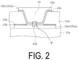
- FIG. 2 is an enlarged explanatory view for illustrating a region X illustrated in FIG. 1 .
- FIG. 3 is an electron micrograph illustrating an example of a region Y illustrated in FIG. 2 .
- the wiring board according to the present disclosure is provided with an alloy layer of metal forming the first wiring conductor layer, tin, and nichrome, between the first via land and the first base layer as described above.
- an alloy layer has a lower Young's modulus than the first base layer formed of nichrome.
- the alloy layer acts as a buffer material between the first via land and the first base layer to reduce the occurrence of cracks between the first via land and the via conductor.
- such an alloy layer is provided to facilitate the connection of crystals of the metal forming the first via land, crystals of the nichrome forming the first base layer, crystals of the metal forming the second base layer, and crystals of the metal forming the via conductor, with continuous crystals.
- the wiring board 1 includes a plurality of insulating layers 11 , a wiring conductor layer 13 located on each surface of the insulating layers 11 and including a via land 131 , a via hole penetrating from the upper surface to the lower surface of the insulating layer 11 , and a via conductor 14 located in the via hole.
- the build-up layer 112 has a thickness of 1 ⁇ m to 60 ⁇ m, for example. The most used thickness is 5 ⁇ m to 20 ⁇ m.
- the build-up layers 112 may be the same resin or different resins.
- the wiring board 1 according to one embodiment is obtained, for example, by a manufacturing method including the following steps (A) to (E):
- (C) A step of forming, by sputtering, a first base layer formed of nichrome on the inner surface of the via hole;
- the wiring conductor layers 13 (for example, first wiring conductor layer 13 a ) are formed on both surfaces of the core layer 111 , and the through-hole conductor 12 is formed in each of the through-holes.
- the wiring conductor layer 13 and the through-hole conductor 12 are formed as follows, for example. Base conductors are formed on both surfaces of the core layer 111 and through-hole wall surfaces by electroless copper plating.
- a plating resist having an opening for forming a wiring pattern is formed by adhering a resist film to each of both surfaces of the core layer 111 and performing exposure and development. After that, electrolytic copper plating is performed to precipitate the copper plated metal in the opening and in the through-hole.
- the plating resist is peeled off, and the base conductor located under the plating resist is removed by etching.
- the wiring conductor layers 13 are formed on the both surfaces of the core layer 111 , and the through-hole conductor 12 is formed in the through-hole.
- the formed wiring conductor layer 13 includes the via land 131 (for example, first via land 131 a ).
- the through-hole conductor 12 formed in the core layer 111 is electrically connected to the wiring conductor layers 13 formed on both surfaces of the core layer 111 .
- a layer 134 containing a coupling agent is formed on the upper surface of the metal layer 133 containing tin.
- the layer 134 containing the coupling agent is formed by depositing the coupling agent on the metal layer 133 containing tin by, for example, immersion treatment to be then heated and dried.
- the coupling agent include silane coupling agents.
- the build-up layers 112 (for example, second insulating layer 11 b ) are formed on the upper and lower surfaces of the core layer 111 to obtain a laminate.
- the build-up layer 112 is formed, for example, by depositing films for the build-up layer 112 under vacuum on each of the upper and lower surfaces of the core layer 111 to be then thermoset.
- the thickness of the build-up layer 112 is as described above, and is, for example, 1 ⁇ m to 60 ⁇ m. The most used thickness is 5 ⁇ m to 20 ⁇ m.
- the build-up layer 112 as well as, the surface of the core layer 111 and the wiring conductor layer 13 formed on the surface of the core layer 111 , are connected via the metal layer 133 containing tin described above and the layer 134 containing the coupling agent.
- the build-up layer 112 thus layered on each of the upper and lower surfaces of the core layer 111 is connected, via the layer 134 containing the coupling agent, to the wiring conductor layer 13 , which improves the adhesion strength to each other.
- via holes penetrating the upper and lower surfaces of the build-up layer 112 are formed in the build-up layer 112 .
- the via holes are formed by a laser such as a CO 2 laser or a UV-YAG laser.
- the inner diameter of the via hole is as described above, and is, for example, 5 ⁇ m to 80 ⁇ m.
- the first base layer 141 is then formed on the inner surface and the bottom of the via hole.
- the first base layer 141 is formed of nichrome and by sputtering.
- the sputtering is performed under a low pressure of 20 Pa or less.
- the board surface temperature at the time of forming the first base layer 141 by sputtering is not particularly limited and is about 120° C. to 150° C. However, for example, the temperature of the bottom of the via hole (surface of the via land 131 ) reaches 250° C. or higher, which is higher than, at least, the melting point 232° C. of tin.
- Such a temperature increase occurs because the sputtered metal impacts the board, whose kinetic energy is then replaced by thermal energy.
- the difference in temperature between the board surface and the bottom of the via hole is due to the fact that heat is transmitted by radiation under a pressure of 20 Pa or less, but the emissivity of the resin portion is close to 1.0.
- the emissivity of the metal portion, especially copper is only 0.1, which is 1/10 of the emissivity of the metal portion, thus it is difficult for heat to escape.
- These temperatures are measured, for example, using a thermocouple connected to the wiring board.
- Sputtering at such a temperature forms the alloy layer 132 of tin contained in the metal layer 133 containing tin present at the bottom of the via hole, that is, on the surface of the via land 131 , and metal (for example, copper) forming the via land 131 (wiring conductor layer 13 ) and nichrome formed by sputtering.
- Such an alloy layer 132 lies at least between the via land 131 and the first base layer 141 .
- the second base layer 142 is formed on the surface of the first base layer 141 .
- the second base layer 142 is formed of the same metal as that forming the via conductor 14 and is formed by sputtering, similar to the first base layer 141 .
- the sputtering is performed under a low pressure of 20 Pa or less.
- the board surface temperature (temperature of the build-up layer 112 on the outermost surface) at the time of forming the second base layer 142 by sputtering is not particularly limited, and is about 180° C. to 200° C.
- the wiring board of the present disclosure is not limited to the embodiment described above.
- the alloy layer 132 is entirely formed between the via land 131 and the first base layer 141 .
- the alloy layer 132 may not necessarily be formed entirely between the via land 131 and the first base layer 141 .
- the alloy layer 132 may be formed intermittently between the via land 131 and the first base layer 141 .
- the wiring board 1 has a build-up structure in which three build-up layers 112 are layered on each of the upper and lower surfaces of the core layer 111 .
- the number of layers of build-up layers 112 may be 1 or 2, or 4 or more.
Landscapes
- Engineering & Computer Science (AREA)
- Microelectronics & Electronic Packaging (AREA)
- Manufacturing & Machinery (AREA)
- Physics & Mathematics (AREA)
- Optics & Photonics (AREA)
- Production Of Multi-Layered Print Wiring Board (AREA)
- Printing Elements For Providing Electric Connections Between Printed Circuits (AREA)
- Manufacturing Of Printed Wiring (AREA)
Abstract
Description
- Patent Document 1: JP 2017-73520 A
- 1 Wiring board
- 11 a First insulating layer
- 11 b Second insulating layer
- 111 Core layer
- 112 Build-up layer
- 12 Through-hole conductor
- 13 a First wiring conductor layer
- 13 b Second wiring conductor layer
- 131 a First via land
- 131 b Second via land
- 132 Alloy layer
- 133 Metal layer containing tin
- 134 Layer containing coupling agent
- 14 Via conductor
- 141 First base layer
- 142 Second base layer
Claims (12)
Applications Claiming Priority (3)
| Application Number | Priority Date | Filing Date | Title |
|---|---|---|---|
| JP2019-197805 | 2019-10-30 | ||
| JP2019197805 | 2019-10-30 | ||
| PCT/JP2020/031575 WO2021084860A1 (en) | 2019-10-30 | 2020-08-21 | Wiring board |
Publications (2)
| Publication Number | Publication Date |
|---|---|
| US20220418098A1 US20220418098A1 (en) | 2022-12-29 |
| US12245366B2 true US12245366B2 (en) | 2025-03-04 |
Family
ID=75715098
Family Applications (1)
| Application Number | Title | Priority Date | Filing Date |
|---|---|---|---|
| US17/771,640 Active 2041-06-02 US12245366B2 (en) | 2019-10-30 | 2020-08-21 | Wiring board |
Country Status (4)
| Country | Link |
|---|---|
| US (1) | US12245366B2 (en) |
| JP (1) | JP7337185B2 (en) |
| KR (1) | KR102752220B1 (en) |
| WO (1) | WO2021084860A1 (en) |
Families Citing this family (1)
| Publication number | Priority date | Publication date | Assignee | Title |
|---|---|---|---|---|
| CN119156895A (en) * | 2022-06-01 | 2024-12-17 | 株式会社村田制作所 | Laminated substrate |
Citations (13)
| Publication number | Priority date | Publication date | Assignee | Title |
|---|---|---|---|---|
| US5227012A (en) * | 1990-04-24 | 1993-07-13 | Hightec Mg Ag | Method of manufacturing multi-layer thin film circuits containing integrated thin film resistors |
| JPH07147483A (en) | 1993-09-30 | 1995-06-06 | Ibiden Co Ltd | Printed wiring board and manufacture thereof |
| US20050258522A1 (en) * | 1998-09-28 | 2005-11-24 | Ibiden Co., Ltd. | Printed wiring board and method for producing the same |
| US20080030965A1 (en) * | 2006-08-04 | 2008-02-07 | Phoenix Precision Technology Corporation | Circuit board structure with capacitors embedded therein and method for fabricating the same |
| US20090223700A1 (en) * | 2008-03-05 | 2009-09-10 | Honeywell International Inc. | Thin flexible circuits |
| US20090242252A1 (en) * | 2008-03-27 | 2009-10-01 | Ibiden Co., Ltd. | Method for Manufacturing A Multilayer Printed Wiring Board for Providing an Electronic Component Therein |
| US20090244865A1 (en) * | 2008-03-27 | 2009-10-01 | Ibiden Co., Ltd | Method for manufacturing multilayer printed wiring board |
| US20110314666A1 (en) * | 2010-04-27 | 2011-12-29 | Kyocera Corporation | Method for manufacturing circuit board and method for manufacturing structure using the same |
| JP2012074687A (en) | 2010-08-31 | 2012-04-12 | Kyocera Corp | Manufacturing method of wiring board and manufacturing method of mounting structure thereof |
| JP2016035969A (en) | 2014-08-01 | 2016-03-17 | 味の素株式会社 | Circuit board and method for manufacturing the same |
| JP2017073520A (en) | 2015-10-09 | 2017-04-13 | 新光電気工業株式会社 | WIRING BOARD, SEMICONDUCTOR DEVICE, AND WIRING BOARD MANUFACTURING METHOD |
| US20180376602A1 (en) * | 2015-12-25 | 2018-12-27 | Mitsui Mining & Smelting Co., Ltd. | Copper foil with carrier, copper foil with resin and method for manufacturing printed wiring board |
| US20190371717A1 (en) * | 2018-05-31 | 2019-12-05 | Shinko Electric Industries Co., Ltd. | Interconnect substrate |
Family Cites Families (2)
| Publication number | Priority date | Publication date | Assignee | Title |
|---|---|---|---|---|
| US5127986A (en) * | 1989-12-01 | 1992-07-07 | Cray Research, Inc. | High power, high density interconnect method and apparatus for integrated circuits |
| JP2002324967A (en) * | 2001-04-24 | 2002-11-08 | Ngk Spark Plug Co Ltd | Substrate manufacturing method |
-
2020
- 2020-08-21 US US17/771,640 patent/US12245366B2/en active Active
- 2020-08-21 WO PCT/JP2020/031575 patent/WO2021084860A1/en not_active Ceased
- 2020-08-21 JP JP2021554103A patent/JP7337185B2/en active Active
- 2020-08-21 KR KR1020227012817A patent/KR102752220B1/en active Active
Patent Citations (14)
| Publication number | Priority date | Publication date | Assignee | Title |
|---|---|---|---|---|
| US5227012A (en) * | 1990-04-24 | 1993-07-13 | Hightec Mg Ag | Method of manufacturing multi-layer thin film circuits containing integrated thin film resistors |
| JPH07147483A (en) | 1993-09-30 | 1995-06-06 | Ibiden Co Ltd | Printed wiring board and manufacture thereof |
| US20050258522A1 (en) * | 1998-09-28 | 2005-11-24 | Ibiden Co., Ltd. | Printed wiring board and method for producing the same |
| US20080030965A1 (en) * | 2006-08-04 | 2008-02-07 | Phoenix Precision Technology Corporation | Circuit board structure with capacitors embedded therein and method for fabricating the same |
| US20090223700A1 (en) * | 2008-03-05 | 2009-09-10 | Honeywell International Inc. | Thin flexible circuits |
| US20090242252A1 (en) * | 2008-03-27 | 2009-10-01 | Ibiden Co., Ltd. | Method for Manufacturing A Multilayer Printed Wiring Board for Providing an Electronic Component Therein |
| US20090244865A1 (en) * | 2008-03-27 | 2009-10-01 | Ibiden Co., Ltd | Method for manufacturing multilayer printed wiring board |
| US20110314666A1 (en) * | 2010-04-27 | 2011-12-29 | Kyocera Corporation | Method for manufacturing circuit board and method for manufacturing structure using the same |
| JP2012074687A (en) | 2010-08-31 | 2012-04-12 | Kyocera Corp | Manufacturing method of wiring board and manufacturing method of mounting structure thereof |
| JP2016035969A (en) | 2014-08-01 | 2016-03-17 | 味の素株式会社 | Circuit board and method for manufacturing the same |
| JP2017073520A (en) | 2015-10-09 | 2017-04-13 | 新光電気工業株式会社 | WIRING BOARD, SEMICONDUCTOR DEVICE, AND WIRING BOARD MANUFACTURING METHOD |
| US20170103942A1 (en) * | 2015-10-09 | 2017-04-13 | Shinko Electric Industries Co., Ltd. | Wiring substrate and semiconductor device |
| US20180376602A1 (en) * | 2015-12-25 | 2018-12-27 | Mitsui Mining & Smelting Co., Ltd. | Copper foil with carrier, copper foil with resin and method for manufacturing printed wiring board |
| US20190371717A1 (en) * | 2018-05-31 | 2019-12-05 | Shinko Electric Industries Co., Ltd. | Interconnect substrate |
Also Published As
| Publication number | Publication date |
|---|---|
| JP7337185B2 (en) | 2023-09-01 |
| KR102752220B1 (en) | 2025-01-10 |
| KR20220065014A (en) | 2022-05-19 |
| WO2021084860A1 (en) | 2021-05-06 |
| US20220418098A1 (en) | 2022-12-29 |
| JPWO2021084860A1 (en) | 2021-05-06 |
Similar Documents
| Publication | Publication Date | Title |
|---|---|---|
| US10790209B2 (en) | Wiring circuit substrate, semiconductor device, method of producing the wiring circuit substrate, and method of producing the semiconductor device | |
| US9253897B2 (en) | Wiring substrate and method for manufacturing the same | |
| JP6840935B2 (en) | Wiring circuit board manufacturing method | |
| WO2011002022A1 (en) | Printed circuit board and manufacturing method of printed circuit board | |
| TWI462668B (en) | Printed circuit board manufacturing method and printed circuit board | |
| US9711440B2 (en) | Wiring board and method for manufacturing the same | |
| JP6301812B2 (en) | Wiring board and manufacturing method thereof | |
| TW200913098A (en) | Semiconductor plastic package and fabricating method thereof | |
| WO2006082784A1 (en) | Multilayer printed wiring board | |
| US20120199386A1 (en) | Multilayer printed wiring board | |
| US20160330836A1 (en) | Printed wiring board | |
| KR20140020114A (en) | Metal heat-radiation substrate and manufacturing method thereof | |
| JP2009295850A (en) | Method of manufacturing multi-layer circuit board, multi-layer circuit board obtained by the same, semiconductor chip-mounted substrate, and semiconductor package using this substrate | |
| JP2015170769A (en) | Printed wiring board and printed wiring board manufacturing method | |
| US11871525B2 (en) | Wiring board and manufacturing method for same | |
| US12245366B2 (en) | Wiring board | |
| JP2005039233A (en) | Substrate having via hole and its producing process | |
| TWI595811B (en) | Printed circuit board and method for manufacturing the same | |
| JP7234049B2 (en) | printed wiring board | |
| JP3674662B2 (en) | Wiring board manufacturing method | |
| CN104737631B (en) | The manufacture method and printed wiring board of printed wiring board | |
| JP2017063152A (en) | Wiring board and manufacturing method of the same | |
| TWI803002B (en) | Wiring substrate | |
| CN110958762B (en) | Printed wiring board | |
| US20240324103A1 (en) | Wiring substrate |
Legal Events
| Date | Code | Title | Description |
|---|---|---|---|
| AS | Assignment |
Owner name: KYOCERA CORPORATION, JAPAN Free format text: ASSIGNMENT OF ASSIGNORS INTEREST;ASSIGNOR:YUGAWA, HIDETOSHI;REEL/FRAME:059699/0213 Effective date: 20200825 |
|
| FEPP | Fee payment procedure |
Free format text: ENTITY STATUS SET TO UNDISCOUNTED (ORIGINAL EVENT CODE: BIG.); ENTITY STATUS OF PATENT OWNER: LARGE ENTITY |
|
| STPP | Information on status: patent application and granting procedure in general |
Free format text: DOCKETED NEW CASE - READY FOR EXAMINATION |
|
| STPP | Information on status: patent application and granting procedure in general |
Free format text: NON FINAL ACTION MAILED |
|
| STPP | Information on status: patent application and granting procedure in general |
Free format text: RESPONSE TO NON-FINAL OFFICE ACTION ENTERED AND FORWARDED TO EXAMINER |
|
| STPP | Information on status: patent application and granting procedure in general |
Free format text: NOTICE OF ALLOWANCE MAILED -- APPLICATION RECEIVED IN OFFICE OF PUBLICATIONS |
|
| ZAAB | Notice of allowance mailed |
Free format text: ORIGINAL CODE: MN/=. |
|
| STPP | Information on status: patent application and granting procedure in general |
Free format text: AWAITING TC RESP., ISSUE FEE NOT PAID |
|
| STPP | Information on status: patent application and granting procedure in general |
Free format text: AWAITING TC RESP, ISSUE FEE PAYMENT VERIFIED |
|
| STPP | Information on status: patent application and granting procedure in general |
Free format text: PUBLICATIONS -- ISSUE FEE PAYMENT VERIFIED |
|
| STCF | Information on status: patent grant |
Free format text: PATENTED CASE |