US11774239B1 - Optical measurement device and calibration method thereof - Google Patents
Optical measurement device and calibration method thereof Download PDFInfo
- Publication number
- US11774239B1 US11774239B1 US17/662,842 US202217662842A US11774239B1 US 11774239 B1 US11774239 B1 US 11774239B1 US 202217662842 A US202217662842 A US 202217662842A US 11774239 B1 US11774239 B1 US 11774239B1
- Authority
- US
- United States
- Prior art keywords
- pattern
- stage
- lens group
- imaging lens
- light
- Prior art date
- Legal status (The legal status is an assumption and is not a legal conclusion. Google has not performed a legal analysis and makes no representation as to the accuracy of the status listed.)
- Active, expires
Links
- 230000003287 optical effect Effects 0.000 title claims abstract description 98
- 238000000034 method Methods 0.000 title claims abstract description 27
- 238000005259 measurement Methods 0.000 title claims description 58
- 238000003384 imaging method Methods 0.000 claims abstract description 87
- 238000004458 analytical method Methods 0.000 description 2
- 238000007796 conventional method Methods 0.000 description 2
- 230000004075 alteration Effects 0.000 description 1
- 239000011248 coating agent Substances 0.000 description 1
- 238000000576 coating method Methods 0.000 description 1
- 238000010276 construction Methods 0.000 description 1
- 230000007547 defect Effects 0.000 description 1
- 239000005357 flat glass Substances 0.000 description 1
- 238000006467 substitution reaction Methods 0.000 description 1
Images


Classifications
-
- G—PHYSICS
- G01—MEASURING; TESTING
- G01B—MEASURING LENGTH, THICKNESS OR SIMILAR LINEAR DIMENSIONS; MEASURING ANGLES; MEASURING AREAS; MEASURING IRREGULARITIES OF SURFACES OR CONTOURS
- G01B21/00—Measuring arrangements or details thereof, where the measuring technique is not covered by the other groups of this subclass, unspecified or not relevant
- G01B21/02—Measuring arrangements or details thereof, where the measuring technique is not covered by the other groups of this subclass, unspecified or not relevant for measuring length, width, or thickness
- G01B21/04—Measuring arrangements or details thereof, where the measuring technique is not covered by the other groups of this subclass, unspecified or not relevant for measuring length, width, or thickness by measuring coordinates of points
- G01B21/042—Calibration or calibration artifacts
-
- G—PHYSICS
- G01—MEASURING; TESTING
- G01N—INVESTIGATING OR ANALYSING MATERIALS BY DETERMINING THEIR CHEMICAL OR PHYSICAL PROPERTIES
- G01N21/00—Investigating or analysing materials by the use of optical means, i.e. using sub-millimetre waves, infrared, visible or ultraviolet light
- G01N21/01—Arrangements or apparatus for facilitating the optical investigation
-
- G—PHYSICS
- G01—MEASURING; TESTING
- G01B—MEASURING LENGTH, THICKNESS OR SIMILAR LINEAR DIMENSIONS; MEASURING ANGLES; MEASURING AREAS; MEASURING IRREGULARITIES OF SURFACES OR CONTOURS
- G01B11/00—Measuring arrangements characterised by the use of optical techniques
- G01B11/26—Measuring arrangements characterised by the use of optical techniques for measuring angles or tapers; for testing the alignment of axes
-
- G—PHYSICS
- G01—MEASURING; TESTING
- G01B—MEASURING LENGTH, THICKNESS OR SIMILAR LINEAR DIMENSIONS; MEASURING ANGLES; MEASURING AREAS; MEASURING IRREGULARITIES OF SURFACES OR CONTOURS
- G01B11/00—Measuring arrangements characterised by the use of optical techniques
- G01B11/02—Measuring arrangements characterised by the use of optical techniques for measuring length, width or thickness
-
- G—PHYSICS
- G01—MEASURING; TESTING
- G01B—MEASURING LENGTH, THICKNESS OR SIMILAR LINEAR DIMENSIONS; MEASURING ANGLES; MEASURING AREAS; MEASURING IRREGULARITIES OF SURFACES OR CONTOURS
- G01B11/00—Measuring arrangements characterised by the use of optical techniques
- G01B11/26—Measuring arrangements characterised by the use of optical techniques for measuring angles or tapers; for testing the alignment of axes
- G01B11/27—Measuring arrangements characterised by the use of optical techniques for measuring angles or tapers; for testing the alignment of axes for testing the alignment of axes
- G01B11/272—Measuring arrangements characterised by the use of optical techniques for measuring angles or tapers; for testing the alignment of axes for testing the alignment of axes using photoelectric detection means
-
- G—PHYSICS
- G01—MEASURING; TESTING
- G01B—MEASURING LENGTH, THICKNESS OR SIMILAR LINEAR DIMENSIONS; MEASURING ANGLES; MEASURING AREAS; MEASURING IRREGULARITIES OF SURFACES OR CONTOURS
- G01B11/00—Measuring arrangements characterised by the use of optical techniques
- G01B11/28—Measuring arrangements characterised by the use of optical techniques for measuring areas
-
- G—PHYSICS
- G01—MEASURING; TESTING
- G01B—MEASURING LENGTH, THICKNESS OR SIMILAR LINEAR DIMENSIONS; MEASURING ANGLES; MEASURING AREAS; MEASURING IRREGULARITIES OF SURFACES OR CONTOURS
- G01B11/00—Measuring arrangements characterised by the use of optical techniques
- G01B11/02—Measuring arrangements characterised by the use of optical techniques for measuring length, width or thickness
- G01B11/022—Measuring arrangements characterised by the use of optical techniques for measuring length, width or thickness by means of tv-camera scanning
-
- G—PHYSICS
- G01—MEASURING; TESTING
- G01B—MEASURING LENGTH, THICKNESS OR SIMILAR LINEAR DIMENSIONS; MEASURING ANGLES; MEASURING AREAS; MEASURING IRREGULARITIES OF SURFACES OR CONTOURS
- G01B11/00—Measuring arrangements characterised by the use of optical techniques
- G01B11/02—Measuring arrangements characterised by the use of optical techniques for measuring length, width or thickness
- G01B11/06—Measuring arrangements characterised by the use of optical techniques for measuring length, width or thickness for measuring thickness ; e.g. of sheet material
-
- G—PHYSICS
- G01—MEASURING; TESTING
- G01N—INVESTIGATING OR ANALYSING MATERIALS BY DETERMINING THEIR CHEMICAL OR PHYSICAL PROPERTIES
- G01N21/00—Investigating or analysing materials by the use of optical means, i.e. using sub-millimetre waves, infrared, visible or ultraviolet light
- G01N21/01—Arrangements or apparatus for facilitating the optical investigation
- G01N2021/0106—General arrangement of respective parts
- G01N2021/0112—Apparatus in one mechanical, optical or electronic block
-
- G—PHYSICS
- G01—MEASURING; TESTING
- G01N—INVESTIGATING OR ANALYSING MATERIALS BY DETERMINING THEIR CHEMICAL OR PHYSICAL PROPERTIES
- G01N21/00—Investigating or analysing materials by the use of optical means, i.e. using sub-millimetre waves, infrared, visible or ultraviolet light
- G01N21/17—Systems in which incident light is modified in accordance with the properties of the material investigated
- G01N21/41—Refractivity; Phase-affecting properties, e.g. optical path length
- G01N21/43—Refractivity; Phase-affecting properties, e.g. optical path length by measuring critical angle
Definitions
- the present disclosure relates to an optical measurement device and a calibration method of the optical measurement device.
- a conventional method may dispose a level on the stage and adjust screws around the stage to make sure the stage is parallel to the ground.
- this conventional method does not calibrate the positions of the optical measuring device and the stage, so we have no idea whether an optical axis of the imaging lens group is parallel to the normal direction of the stage.
- the measured size is on the order of microns, it requires very high measurement accuracy. A slight position shift will cause errors in the measurement results. So, it is necessary to calibrate the imaging lens group to make sure the optical axis is parallel to the normal direction of the stage.
- An aspect of the present disclosure is related to a calibration method of an optical measurement device.
- a calibration method of an optical measurement device includes: disposing an object on a stage, wherein the object has a top surface and a bottom surface opposite to the top surface, the top surface has a first pattern, and the bottom surface has a second pattern; emitting an incident light to the object on the stage, wherein a first light is reflected after the incident light passes through the first pattern, and a second light is reflected after the incident light passes through the second pattern; receiving the first light and the second light by an imaging lens group to obtain a third pattern corresponding to the first pattern and a fourth pattern corresponding to the second pattern; transmitting the third pattern and the fourth pattern to an image sensor by the imaging lens group, wherein a center point of the third pattern and a center point of the fourth pattern are separated by a first distance on the image sensor; calculating a tilted angle between an optical axis of the imaging lens group and a normal direction of the stage according to the first distance; and adjusting the stage according to the tilted angle such that the normal direction of
- the method further includes calculating the tilted angle according to a thickness between the top surface and the bottom surface of the object.
- the method further includes calculating the tilted angle according a refractive index of the object.
- the method further includes calculating the tilted angle according to a magnification of the imaging lens group.
- the method further includes calculating a second distance between the first light and the second light according to the first distance, the tilted angle and the magnification.
- emitting the incident light to the object on the stage further includes: emitting the incident light to a beam splitter of the imaging lens group by a coaxial light source; and reflecting the incident light to the object on the stage by the beam splitter.
- the method further includes determining a first direction from the third pattern to the fourth pattern on the image sensor.
- the method further includes moving the stage along a second direction, wherein the second direction is opposite to the first direction.
- Another aspect of the present disclosure is related to an optical measurement device.
- an optical measurement device includes a stage, an object, a coaxial light source, a imaging lens group, an image sensor and a calculation unit.
- the object is disposed on the stage.
- the object has a top surface and a bottom surface opposite to the top surface.
- the top surface has a first pattern.
- the bottom surface has a second pattern.
- the coaxial light source is configured to emit an incident light to the object on the stage.
- the imaging lens group is located at one side of the coaxial light source.
- the imaging lens group is configured to receive a first light reflected by the first pattern and a second light reflected by the second pattern from the incident light to obtain a third pattern corresponding to the first pattern and a fourth pattern corresponding to the second pattern.
- the image sensor is located at one side of the imaging lens group facing away from the stage.
- the image sensor is configured to receive the third pattern and the fourth pattern.
- a center point of the third pattern and a center point of the fourth pattern are separated by a first distance on the image sensor.
- the calculation unit electrically is connected to the stage.
- the calculation unit electrically is configured to calculate a tilted angle between an optical axis of the imaging lens group and a normal direction of the stage according to the first distance and adjust the stage according to the tilted angle such that the normal direction of the stage is parallel to the optical axis of the imaging lens group.
- the imaging lens group has a beam splitter, and the beam splitter is located between the image sensor and the object.
- the beam splitter is configured to reflect the incident light to the object on the stage.
- the object is located between the stage and the imaging lens group.
- the object has a thickness between the top surface and the bottom surface.
- the calculation unit is further configured to calculate the tilted angle between the optical axis of the imaging lens group and the normal direction of the stage according to the thickness.
- the object has a refractive index.
- the calculation unit is further configured to calculate the tilted angle between the optical axis of the imaging lens group and the normal direction of the stage according to the refractive index of the object.
- the imaging lens group has a magnification.
- the calculation unit is further configured to calculate the tilted angle between the optical axis of the imaging lens group and the normal direction of the stage according to the magnification of the imaging lens group.
- the calculation unit is further configured to calculate a second distance between the first light and the second light according to the first distance, the tilted angle and the magnification.
- the calculation unit is further configured to determine a first direction from the third pattern to the fourth pattern on the image sensor.
- the stage is further configured to move along a second direction opposite to the first direction.
- an included angle between the incident light and the first light is twice the tilted angle.
- the optical measurement device may calculate the tilted angle between the optical axis of the imaging lens group and the normal direction of the stage according to the first distance. Moreover, the optical measurement device may adjust the stage according to the tilted angle. Therefore, the normal direction of the stage of the optical measurement device may be corrected to be parallel to the optical axis of the imaging lens group, which may improve the measurement accuracy of the optical measurement device for measuring the object.
- the optical measurement device may be used in micron-level measurement systems that require high measurement accuracy.
- FIG. 1 illustrates a schematic view of an optical measurement device according to one embodiment of the present disclosure.
- FIG. 2 illustrates a stereoscopic view of an object according to one embodiment of the present disclosure.
- FIG. 3 illustrates a schematic view of a tilted angle between an optical axis of an imaging lens group and a normal direction of an object according to one embodiment of the present disclosure.
- FIG. 4 illustrates a schematic view of a third pattern and a fourth pattern on an image sensor according to one embodiment of the present disclosure.
- FIG. 5 illustrates a flow chart of a calibration method of an optical measurement device according to one embodiment of the present disclosure.
- FIG. 6 A illustrates a schematic view a third pattern and a fourth pattern are shifted according to one embodiment of the present disclosure.
- FIGS. 6 B, 7 and 8 illustrate schematic views of calibrating a third pattern and a fourth pattern according to some embodiments of the present disclosure.
- spatially relative terms such as “beneath,” “below,” “lower,” “above,” “upper,” “front,” “back” and the like, may be used herein for ease of description to describe one element or feature's relationship to another element(s) or feature(s) as illustrated in the figures.
- the spatially relative terms are intended to encompass different orientations of the device in use or operation in addition to the orientation depicted in the figures.
- the apparatus may be otherwise oriented (rotated 90 degrees or at other orientations) and the spatially relative descriptors used herein may likewise be interpreted accordingly.
- FIG. 1 illustrates a schematic view of an optical measurement device 100 according to one embodiment of the present disclosure.
- FIG. 2 illustrates a stereoscopic view of an object 120 according to one embodiment of the present disclosure.
- the optical measurement device 100 includes a stage 110 , the object 120 , a coaxial light source 130 , an imaging lens group 140 , an image sensor 150 and a calculation unit 160 .
- the object 120 is disposed on stage 110 .
- the object 120 may be a flat glass certified by the National Measurement Center, but it is not limited in this regard.
- the object 120 has a top surface 122 and a bottom surface 124 opposite to top surface 122 .
- the top surface 122 of the object 120 may be parallel to the bottom surface 124 , and the top surface 122 has a first pattern P 1 .
- the bottom surface 124 of the object 120 has a second pattern P 2 .
- the first pattern P 1 and the second pattern P 2 may have high reflection characteristics to reflect light (it will be described in detail below).
- the coaxial light source 130 is configured to emit incident light 132 to object 120 on stage 110 .
- the coaxial light source 130 may provide the more uniform incident light 132 to avoid reflection of the object 120 , thereby improving an image capturing accuracy of the imaging lens group 140 .
- FIG. 3 illustrates a schematic view of a tilted angle ⁇ between an optical axis a of the imaging lens group 140 and a normal direction 112 of the object 120 according to one embodiment of the present disclosure.
- the stage 110 , the coaxial light source 130 and the imaging lens group 140 in FIG. 1 are omitted here.
- the imaging lens group 140 is located at one side 142 of the coaxial light source 130 . Since the object 120 is disposed horizontally on the stage 110 , the normal direction 112 of the object 120 is the same as the stage 110 .
- the object 120 disposed on the stage 110 also has the same tilted angle ⁇ with respect to the optical axis a of the imaging lens group 140 .
- the imaging lens group 140 is configured to receive a first light 136 reflected by the first pattern P 1 and a second light 138 reflected by the second pattern P 2 from the incident light 132 . That is, when the incident light 132 is incident on the object 120 having the tilted angle ⁇ , an included angle between the first light 136 and the incident light 132 is twice the tilted angle ⁇ (ie, 2 ⁇ ).
- FIG. 4 illustrates a schematic view of a third pattern P 3 and a fourth pattern P 4 on the image sensor 150 according to one embodiment of the present disclosure.
- the imaging lens group 140 is configured to obtain the third pattern P 3 corresponding to the first pattern P 1 and the fourth pattern P 4 corresponding to the second pattern P 2 .
- the image sensor 150 is located at one side 142 of the imaging lens group 140 facing away from the stage 110 .
- the image sensor 150 is configured to receive the third pattern P 3 and the fourth pattern P 4 .
- the calculation unit 160 is electrically connected to the stage 110 .
- the calculation unit 160 is configured to calculate the tilted angle ⁇ between the optical axis a of the imaging lens group 140 and the normal direction 112 of the stage 110 according to the first distance d1.
- the calculation unit 160 is configured to adjust the stage 110 according to the tilted angle ⁇ such that the normal direction 112 is parallel to the optical axis a of the imaging lens group 140 , as shown in FIG. 1 .
- the calculation unit 160 of the optical measurement device 100 may calculate the tilted angle ⁇ between the optical axis a of the imaging lens group 140 and the normal direction 112 of the stage 110 according to the first distance d1. Moreover, the optical measurement device 100 may adjust the stage 110 according to the tilted angle ⁇ . Therefore, the normal direction 112 of the stage 110 of the optical measurement device 100 may be corrected to be parallel to the optical axis a of the imaging lens group 140 , which may improve the measurement accuracy of the optical measurement device 100 for measuring the object 120 .
- the optical measurement device 100 may be used in micron-level measurement systems that require high measurement accuracy.
- the imaging lens group 140 has a beam splitter 144 .
- the beam splitter 144 is located between the image sensor 150 and the object 120 .
- the beam splitter 144 of the imaging lens group 140 is configured to reflect the incident light 132 to the object 120 on the stage 110 .
- the beam splitter 144 may be made of optical coating, but it is not limited in this regard.
- the object 120 is located between the stage 110 and the imaging lens group 140 .
- the object 120 has a thickness h between the top surface 122 and the bottom surface 124 .
- the calculation unit 160 is further configured to calculate the tilted angle ⁇ between the optical axis a of the imaging lens group 140 and the normal direction 112 of the stage 110 according to the thickness h.
- the object 120 has a refractive index, and the calculation unit 160 is further configured to calculate the tilted angle ⁇ between the optical axis a of the imaging lens group 140 and the normal direction 112 of the stage 110 according to the refractive index of the object 120 .
- the imaging lens group 140 has a magnification
- the calculation unit 160 is further configured to calculate the tilted angle ⁇ between the optical axis a of the imaging lens group 140 and the normal direction 112 of the stage 110 according to the magnification of the imaging lens group 140 .
- the refractive index of the object 120 may be n
- the magnification of the imaging lens group 140 may be M
- the formula of the tilted angle ⁇ , the magnification M, the thickness h, the refractive index n and the first distance d1 may be:
- the calculation unit 160 may obtain the tilted angle ⁇ through the numerical analysis method (the above formula).
- the stage 110 may be adjusted according to the tilted angle ⁇ such that the normal direction 112 of the stage 110 of the optical measuring device 100 is parallel to the optical axis a of the imaging lens group 140 , so as to improve the measurement accuracy of the optical measuring device 100 .
- the calculation unit 160 is further configured to calculate the second distance d2 between the first light 136 and the second light 138 according to the first distance d1, the tilted angle ⁇ and the magnification M.
- a formula may be:
- the calculation unit 160 may obtain the second distance d2.
- FIG. 5 illustrates a flow chart of a calibration method of an optical measurement device according to one embodiment of the present disclosure.
- the calibration method of the optical measurement device includes steps as outlined below.
- step S1 an object is disposed on a stage, wherein the object has a top surface and a bottom surface opposite to the top surface, the top surface has a first pattern, and the bottom surface has a second pattern.
- step S2 an incident light is emitted to the object on the stage, wherein a first light is reflected after the incident light passes through the first pattern, and a second light is reflected after the incident light passes through the second pattern.
- step S3 the first light and the second light are received by an imaging lens group to obtain a third pattern corresponding to the first pattern and a fourth pattern corresponding to the second pattern.
- step S4 the third pattern and the fourth pattern are transmitted to an image sensor by the imaging lens group, wherein a center point of the third pattern and a center point of the fourth pattern are separated by a first distance on the image sensor.
- step S5 a tilted angle between an optical axis of the imaging lens group and a normal direction of the stage is calculated according to the first distance.
- step S6 the stage is adjusted according to the tilted angle such that the normal direction of the stage is parallel to the optical axis of the imaging lens group.
- the object 120 is disposed on the stage 110 , wherein the object 120 has the top surface 122 and the bottom surface 124 opposite to the top surface 122 .
- the top surface 122 of the object 120 has the first pattern P 1 .
- the bottom surface 124 of the object 120 has the second pattern P 2 .
- the first pattern P 1 and the second pattern P 2 may have high reflection characteristics.
- the incident light 132 is emitted to the object 120 on the stage 110 .
- the first light 136 is reflected after the incident light 132 passes through the first pattern P 1 .
- the second light 138 is reflected after the incident light 132 passes through the second pattern P 2 .
- the incident light 132 is incident on the object 120 having the tilted angle ⁇
- the included angle between the first light 136 and the incident light 132 is twice the tilted angle ⁇ (ie, 2 ⁇ ).
- the first light 136 and the second light 138 are received by the imaging lens group 140 to obtain the third pattern P 3 corresponding to the first pattern P 1 and the fourth pattern P 4 corresponding to the second pattern P 2 .
- the third pattern P 3 and the fourth pattern P 4 are transmitted to the image sensor 150 by the imaging lens group 140 .
- the incident light 132 is incident on the object 120 having the tilted angle ⁇
- the center point C 3 of the third pattern P 3 and the center point C 4 of the fourth pattern P 4 are separated by the first distance d1 on the image sensor 150 .
- the tilted angle ⁇ between the optical axis a of the imaging lens group 140 and the normal direction 112 of the stage 110 is calculated according to the first distance d1, and the stage 110 is adjusted according to the tilted angle ⁇ such that the normal direction 112 is parallel to the optical axis a of the imaging lens group 140 , as shown in FIG. 1 .
- calculating the tilted angle ⁇ between the optical axis a of the imaging lens group 140 and the normal direction 112 of the stage 110 according to the first distance d1 further includes calculating the tilted angle ⁇ according to the thickness h between the top surface 122 and the bottom surface 124 of the object 120 .
- Calculating the tilted angle ⁇ between the optical axis of the imaging lens group 140 and the normal direction 112 of the stage 110 according to the first distance d1 further includes calculating the tilted angle ⁇ according to the refractive index of the object 120 .
- Calculating the tilted angle ⁇ between the optical axis a of the imaging lens group 140 and the normal direction 112 of the stage 110 according to the first distance d1 further includes calculating the tilted angle ⁇ according to the magnification of the imaging lens group 140 .
- the refractive index of the object 120 may be n
- the magnification of the imaging lens group 140 may be M
- the formula of the tilted angle ⁇ , the magnification M, the thickness h, the refractive index n and the first distance d1 may be:
- the calculation unit 160 may obtain the tilted angle ⁇ through the numerical analysis method (the above formula).
- the stage 110 may be adjusted according to the tilted angle ⁇ such that the normal direction 112 of the stage 110 of the optical measuring device 100 is parallel to the optical axis a of the imaging lens group 140 , so as to improve the measurement accuracy of the optical measuring device 100 .
- the calibration method further includes calculating the second distance d2 between the first light 136 and the second light 138 according to the first distance d1, the tilted angle ⁇ and the magnification.
- transmitting the incident light 132 to the object 120 on the stage 110 further includes: transmitting the incident light 132 to the beam splitter 144 of the imaging lens group 140 through the coaxial light source 130 ; and reflecting the incident light 132 to the object 120 on the stage 110 through the beam splitter 144 .
- FIG. 6 A illustrates a schematic view the third pattern P 3 and the fourth pattern P 4 are shifted according to one embodiment of the present disclosure.
- FIGS. 6 B, 7 and 8 illustrate schematic views of calibrating the third pattern P 3 and the fourth pattern P 4 according to some embodiments of the present disclosure.
- the calibration method further includes determining a first direction D 1 from the third pattern P 3 to the fourth pattern P 4 on the image sensor 150 by the calculation unit 160 .
- the coordinates of the center point C 3 may be (217, 159), and the coordinates of the center point C 4 may be (1217, 159), so the calculation unit 160 may determine that the first direction D 1 is rightward, that is, the stage 110 moves toward the right.
- the calibration method further includes moving the stage 110 along a second direction D 2 opposite to the first direction D 1 . That is, the stage 110 may be adjusted to tilt toward the left, so that the normal direction 112 of the stage 110 of the optical measuring device 100 may be parallel to the optical axis a of the imaging lens group 140 , so as to improve the measurement accuracy of the optical measuring device 100 .
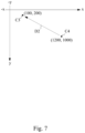
- the coordinates of the center point C 3 may be (100, 200), and the coordinates of the center point C 4 may be (1200, 1000), that is, the calculation unit 160 may determine that the stage 110 is tilted downward to the right. Therefore, the stage 110 may be adjusted to tilt toward the second direction D 2 (toward upper left direction), so that the normal direction 112 of the stage 110 of the optical measuring device 100 may be parallel to the optical axis a of the imaging lens group 140 .
- the coordinates of the center point C 3 may be (303, 650), and the coordinates of the center point C 4 may be (303, 1150), that is, the calculation unit 160 may determine that the stage 110 is tilted downward. Therefore, the stage 110 may be adjusted to tilted along the second direction D 2 (upward direction), so that the normal direction 112 of the stage 110 of the optical measuring device 100 may be parallel to the optical axis a of the imaging lens group 140 .
- the optical measurement device may calculate the tilted angle between the optical axis of the imaging lens group and the normal direction of the stage according to the first distance. Moreover, the optical measurement device may adjust the stage according to the tilted angle. Therefore, the normal direction of the stage of the optical measurement device may be corrected to be parallel to the optical axis of the imaging lens group, which may improve the measurement accuracy of the optical measurement device for measuring the object.
- the optical measurement device may be used in micron-level measurement systems that require high measurement accuracy.
Landscapes
- Physics & Mathematics (AREA)
- General Physics & Mathematics (AREA)
- Health & Medical Sciences (AREA)
- Life Sciences & Earth Sciences (AREA)
- Chemical & Material Sciences (AREA)
- Analytical Chemistry (AREA)
- Biochemistry (AREA)
- General Health & Medical Sciences (AREA)
- Immunology (AREA)
- Pathology (AREA)
- Length Measuring Devices By Optical Means (AREA)
- Optical Radar Systems And Details Thereof (AREA)
- Investigating Or Analysing Materials By Optical Means (AREA)
Abstract
Description
That is, if the magnification M, the thickness h, the refractive index n and the first distance d1 are known, the
Therefore, it me thickness h, the refractive index n and the tilted angle θ are known, the
That is, if the magnification M, the thickness h, the refractive index n and the first distance d1 are known, the
Claims (19)
Applications Claiming Priority (2)
| Application Number | Priority Date | Filing Date | Title |
|---|---|---|---|
| CN202210299913.2A CN114894712B (en) | 2022-03-25 | 2022-03-25 | Optical measuring equipment and its calibration method |
| CN202210299913.2 | 2022-03-25 |
Publications (2)
| Publication Number | Publication Date |
|---|---|
| US20230304791A1 US20230304791A1 (en) | 2023-09-28 |
| US11774239B1 true US11774239B1 (en) | 2023-10-03 |
Family
ID=82714954
Family Applications (1)
| Application Number | Title | Priority Date | Filing Date |
|---|---|---|---|
| US17/662,842 Active 2042-06-14 US11774239B1 (en) | 2022-03-25 | 2022-05-10 | Optical measurement device and calibration method thereof |
Country Status (3)
| Country | Link |
|---|---|
| US (1) | US11774239B1 (en) |
| CN (1) | CN114894712B (en) |
| TW (1) | TWI819548B (en) |
Citations (5)
| Publication number | Priority date | Publication date | Assignee | Title |
|---|---|---|---|---|
| US20020030823A1 (en) * | 2000-07-26 | 2002-03-14 | Nippon Maxis Co., Ltd. | Method and device for measuring thickness of test object |
| US20180087898A1 (en) * | 2015-05-29 | 2018-03-29 | Nippon Steel & Sumitomo Metal Corporation | Shape inspection apparatus for metallic body and shape inspection method for metallic body |
| US20190101492A1 (en) * | 2016-03-09 | 2019-04-04 | Hamamatsu Photonics K.K. | Measuring device, observing device and measuring method |
| CN111239164A (en) * | 2020-04-02 | 2020-06-05 | 上海御微半导体技术有限公司 | A defect detection device and method thereof |
| US20220005715A1 (en) * | 2020-07-06 | 2022-01-06 | Samsung Electronics Co., Ltd. | Metrology apparatus and method based on diffraction using oblique illumination and method of manufacturing semiconductor device using the metrology method |
Family Cites Families (43)
| Publication number | Priority date | Publication date | Assignee | Title |
|---|---|---|---|---|
| JPS6453101A (en) * | 1987-05-25 | 1989-03-01 | Kurashiki Boseki Kk | Equal tilt angle interference type film thickness gauge |
| JP3518107B2 (en) * | 1995-10-30 | 2004-04-12 | 株式会社ニコン | Automatic tilt correction device for surveying equipment |
| JPH10176927A (en) * | 1996-12-16 | 1998-06-30 | Nikon Corp | Tilt sensor |
| SE9700384D0 (en) * | 1997-02-04 | 1997-02-04 | Biacore Ab | Analytical method and apparatus |
| WO1998050913A1 (en) * | 1997-05-07 | 1998-11-12 | Sony Corporation | Optical pickup device |
| JP4143614B2 (en) * | 2000-03-21 | 2008-09-03 | キヤノン株式会社 | Measuring method |
| JP2004325311A (en) * | 2003-04-25 | 2004-11-18 | Katsura Opto Systems:Kk | Detector and method for detecting inclination of light beam |
| JP4135603B2 (en) * | 2003-09-12 | 2008-08-20 | オムロン株式会社 | Two-dimensional spectroscopic device and film thickness measuring device |
| JP4282500B2 (en) * | 2004-01-29 | 2009-06-24 | 株式会社東芝 | Structure inspection method and semiconductor device manufacturing method |
| JP2005331585A (en) * | 2004-05-18 | 2005-12-02 | Nec Viewtechnology Ltd | Projector having device for measuring distance and tilt angle |
| WO2005116577A1 (en) * | 2004-05-28 | 2005-12-08 | Nikon Corporation | Method of adjusting imaging optical system, imaging device, positional deviation detecting device, mark identifying device and edge position detectinc device |
| US20060285120A1 (en) * | 2005-02-25 | 2006-12-21 | Verity Instruments, Inc. | Method for monitoring film thickness using heterodyne reflectometry and grating interferometry |
| TWI386617B (en) * | 2007-12-31 | 2013-02-21 | Ind Tech Res Inst | Reflective measurement method of film thickness by spectral image system |
| JP5473265B2 (en) * | 2008-07-09 | 2014-04-16 | キヤノン株式会社 | Multilayer structure measuring method and multilayer structure measuring apparatus |
| US8817274B2 (en) * | 2009-06-23 | 2014-08-26 | Bongmin Seo | Thickness variation measuring device, system using same, surface microscope using same, thickness variation measuring method, and surface image acquiring method using same |
| JP2012008308A (en) * | 2010-06-24 | 2012-01-12 | Olympus Corp | Imaging optical system and confocal scanning microscope using the same |
| DE102011081879A1 (en) * | 2010-11-03 | 2012-05-03 | Dr. Johannes Heidenhain Gmbh | Optical angle measuring device |
| EP2780755A4 (en) * | 2011-11-15 | 2015-09-02 | Technion Res & Dev Foundation | Method and system for transmitting light |
| CN103163740B (en) * | 2011-12-14 | 2015-01-21 | 上海微电子装备有限公司 | Position measuring device for tilted object |
| TWI447348B (en) * | 2012-02-10 | 2014-08-01 | Nat Synchrotron Radiation Res Ct | Positioning system and method for precise stage |
| CN103575234B (en) * | 2012-07-20 | 2016-08-24 | 德律科技股份有限公司 | 3D image measuring device |
| TWI460394B (en) * | 2012-07-20 | 2014-11-11 | Test Research Inc | Three-dimensional image measuring apparatus |
| CN203190948U (en) * | 2013-04-22 | 2013-09-11 | 北京京东方光电科技有限公司 | Device for detecting thickness of transparent substrate |
| TWI512868B (en) * | 2013-12-24 | 2015-12-11 | Huang Tian Xing | Image Key Dimension Measurement Calibration Method and System |
| CN105526873A (en) * | 2014-10-23 | 2016-04-27 | 苏州研迪智能科技有限公司 | Holographic material detection system |
| TWI518300B (en) * | 2014-11-26 | 2016-01-21 | 財團法人工業技術研究院 | Optical callibration device and optical callibration method |
| WO2017068813A1 (en) * | 2015-10-23 | 2017-04-27 | 株式会社カツラ・オプト・システムズ | Device for measuring characteristics of optical element |
| US10311299B2 (en) * | 2015-12-21 | 2019-06-04 | Eyelock Llc | Reflected optic camera module for iris recognition in a computing device |
| JP7183155B2 (en) * | 2016-11-02 | 2022-12-05 | コーニング インコーポレイテッド | Defect inspection method and apparatus on transparent substrate |
| KR102490763B1 (en) * | 2017-04-14 | 2023-01-20 | 하마마츠 포토닉스 가부시키가이샤 | Aberration correction method and optical device |
| EP3428751A1 (en) * | 2017-07-12 | 2019-01-16 | Koninklijke Philips N.V. | Measuring position of motion stage |
| TWI672553B (en) * | 2017-07-31 | 2019-09-21 | 大立光電股份有限公司 | Projection lens system, projection apparatus, sensing module and electronic device |
| CN110736721B (en) * | 2018-07-18 | 2022-05-24 | 西安工业大学 | Glass plate refractive index uniformity detection device and detection method based on diffraction grating |
| CN112067559B (en) * | 2019-06-11 | 2023-06-13 | 南开大学 | Method for determining optical constant of material, method and device for expanding material database |
| WO2020255282A1 (en) * | 2019-06-19 | 2020-12-24 | 株式会社日立ハイテク | Defect inspection device and defect inspection device calibration method |
| CN110530821B (en) * | 2019-09-16 | 2021-02-12 | 中国科学院福建物质结构研究所 | A kind of measuring device and measuring method of refractive index of optical material |
| CN110987817B (en) * | 2019-12-24 | 2021-01-19 | 华中科技大学 | Ellipsometer integrating dark field observation based on large-numerical-aperture objective lens and measurement method |
| CN111157541B (en) * | 2020-01-14 | 2023-03-14 | 合肥维信诺科技有限公司 | Optical detection system and optical detection method |
| CN111562678B (en) * | 2020-07-14 | 2020-12-08 | 深圳珑璟光电科技有限公司 | Method for adjusting field angle and near-to-eye display device |
| CN113295699B (en) * | 2020-11-17 | 2024-07-30 | 北京领邦智能装备股份公司 | High-precision imaging system, method, image acquisition device and detection equipment |
| CN112945142B (en) * | 2021-02-02 | 2022-12-06 | 江西应用科技学院 | Object three-dimensional measurement system and method based on structured light |
| CN113465520B (en) * | 2021-08-11 | 2024-12-13 | 西安邮电大学 | System and method for measuring thickness and tilt angle of transparent materials |
| CN113960758B (en) * | 2021-11-04 | 2023-06-02 | 业成科技(成都)有限公司 | Optical imaging system, image capturing device and electronic equipment |
-
2022
- 2022-03-25 CN CN202210299913.2A patent/CN114894712B/en active Active
- 2022-03-30 TW TW111112178A patent/TWI819548B/en active
- 2022-05-10 US US17/662,842 patent/US11774239B1/en active Active
Patent Citations (5)
| Publication number | Priority date | Publication date | Assignee | Title |
|---|---|---|---|---|
| US20020030823A1 (en) * | 2000-07-26 | 2002-03-14 | Nippon Maxis Co., Ltd. | Method and device for measuring thickness of test object |
| US20180087898A1 (en) * | 2015-05-29 | 2018-03-29 | Nippon Steel & Sumitomo Metal Corporation | Shape inspection apparatus for metallic body and shape inspection method for metallic body |
| US20190101492A1 (en) * | 2016-03-09 | 2019-04-04 | Hamamatsu Photonics K.K. | Measuring device, observing device and measuring method |
| CN111239164A (en) * | 2020-04-02 | 2020-06-05 | 上海御微半导体技术有限公司 | A defect detection device and method thereof |
| US20220005715A1 (en) * | 2020-07-06 | 2022-01-06 | Samsung Electronics Co., Ltd. | Metrology apparatus and method based on diffraction using oblique illumination and method of manufacturing semiconductor device using the metrology method |
Also Published As
| Publication number | Publication date |
|---|---|
| TWI819548B (en) | 2023-10-21 |
| CN114894712A (en) | 2022-08-12 |
| TW202338304A (en) | 2023-10-01 |
| CN114894712B (en) | 2023-08-25 |
| US20230304791A1 (en) | 2023-09-28 |
Similar Documents
| Publication | Publication Date | Title |
|---|---|---|
| CN111580072B (en) | Surveying instrument and method of calibrating a surveying instrument | |
| CN108168468B (en) | Focusing photoelectric auto-collimator with laser sighting device inside and sighting method | |
| KR20200108874A (en) | Projection of structured light for mirror surfaces | |
| CN112504169A (en) | Device and method for testing laser receiving and transmitting coaxiality of active photoelectric system | |
| CN101922932A (en) | A Compensation Device for Coordinate Measurement Error of Corner Cube Prism | |
| CN100520295C (en) | Optical inclinometer | |
| CN108507492A (en) | The high-precision wide-dynamic-range measurement method and measuring system on a kind of plane surface transmissive element surface | |
| CN112284302A (en) | Device and method for measuring laser transceiver coaxiality of active optoelectronic system by scanning method | |
| CN114088017A (en) | A kind of customized optical fiber end face angle and flatness detection device and detection method | |
| US11774239B1 (en) | Optical measurement device and calibration method thereof | |
| CN109003306B (en) | Optical axis deflection measuring device and method for vehicle-mounted camera | |
| US20080130014A1 (en) | Displacement Measurement Sensor Using the Confocal Principle with an Optical Fiber | |
| KR101126150B1 (en) | Lens meter | |
| TWI518300B (en) | Optical callibration device and optical callibration method | |
| JP2003050109A (en) | Surface shape measuring device and surface shape measuring method | |
| CN214426950U (en) | Plano-convex optical element center deviation measuring device | |
| CN110702378B (en) | Optical axis pointing detection device and detection method | |
| CN111220095B (en) | A method and device for high-precision detection of the verticality of the optical axis of a diverging beam | |
| CN108151762A (en) | A kind of Portable direct angle prism installation parameter marking apparatus | |
| US12130128B2 (en) | Device and method for measuring curvature radius | |
| CN208333382U (en) | System capable of realizing accurate measurement of high and low point positions of off-axis reflector | |
| KR20220041388A (en) | Optical system calibration method | |
| CN116609040B (en) | Auxiliary device and method for detecting right angle errors of pentaprism | |
| CN110687540A (en) | A method for detecting ranging accuracy of an optical module to be measured | |
| CN120333351B (en) | Multi-axis interferometer parallelism detection system and detection method |
Legal Events
| Date | Code | Title | Description |
|---|---|---|---|
| AS | Assignment |
Owner name: GENERAL INTERFACE SOLUTION LIMITED, TAIWAN Free format text: ASSIGNMENT OF ASSIGNORS INTEREST;ASSIGNORS:YEH, CHAO-YI;ZHOU, JIANGYUN;WANG, SIQI;AND OTHERS;REEL/FRAME:059887/0196 Effective date: 20220427 Owner name: INTERFACE OPTOELECTRONICS (WUXI) CO., LTD., CHINA Free format text: ASSIGNMENT OF ASSIGNORS INTEREST;ASSIGNORS:YEH, CHAO-YI;ZHOU, JIANGYUN;WANG, SIQI;AND OTHERS;REEL/FRAME:059887/0196 Effective date: 20220427 Owner name: INTERFACE OPTOELECTRONICS (SHENZHEN) CO., LTD., CHINA Free format text: ASSIGNMENT OF ASSIGNORS INTEREST;ASSIGNORS:YEH, CHAO-YI;ZHOU, JIANGYUN;WANG, SIQI;AND OTHERS;REEL/FRAME:059887/0196 Effective date: 20220427 Owner name: INTERFACE TECHNOLOGY (CHENGDU) CO., LTD., CHINA Free format text: ASSIGNMENT OF ASSIGNORS INTEREST;ASSIGNORS:YEH, CHAO-YI;ZHOU, JIANGYUN;WANG, SIQI;AND OTHERS;REEL/FRAME:059887/0196 Effective date: 20220427 |
|
| FEPP | Fee payment procedure |
Free format text: ENTITY STATUS SET TO UNDISCOUNTED (ORIGINAL EVENT CODE: BIG.); ENTITY STATUS OF PATENT OWNER: LARGE ENTITY |
|
| STCF | Information on status: patent grant |
Free format text: PATENTED CASE |
|
| AS | Assignment |
Owner name: GENERAL INTERFACE SOLUTION LIMITED, TAIWAN Free format text: ASSIGNMENT OF ASSIGNORS INTEREST;ASSIGNORS:INTERFACE TECHNOLOGY (CHENGDU) CO., LTD.;INTERFACE OPTOELECTRONICS (SHENZHEN) CO., LTD.;INTERFACE OPTOELECTRONICS (WUXI) CO., LTD.;AND OTHERS;REEL/FRAME:066509/0025 Effective date: 20231210 Owner name: INTERFACE OPTOELECTRONICS (SHENZHEN) CO., LTD., CHINA Free format text: ASSIGNMENT OF ASSIGNORS INTEREST;ASSIGNORS:INTERFACE TECHNOLOGY (CHENGDU) CO., LTD.;INTERFACE OPTOELECTRONICS (SHENZHEN) CO., LTD.;INTERFACE OPTOELECTRONICS (WUXI) CO., LTD.;AND OTHERS;REEL/FRAME:066509/0025 Effective date: 20231210 Owner name: INTERFACE TECHNOLOGY (CHENGDU) CO., LTD., CHINA Free format text: ASSIGNMENT OF ASSIGNORS INTEREST;ASSIGNORS:INTERFACE TECHNOLOGY (CHENGDU) CO., LTD.;INTERFACE OPTOELECTRONICS (SHENZHEN) CO., LTD.;INTERFACE OPTOELECTRONICS (WUXI) CO., LTD.;AND OTHERS;REEL/FRAME:066509/0025 Effective date: 20231210 |