US11605951B2 - Photovoltaic converter string, control method, and system - Google Patents
Photovoltaic converter string, control method, and system Download PDFInfo
- Publication number
- US11605951B2 US11605951B2 US17/362,119 US202117362119A US11605951B2 US 11605951 B2 US11605951 B2 US 11605951B2 US 202117362119 A US202117362119 A US 202117362119A US 11605951 B2 US11605951 B2 US 11605951B2
- Authority
- US
- United States
- Prior art keywords
- switching transistor
- buck
- boost circuit
- photovoltaic
- photovoltaic converter
- Prior art date
- Legal status (The legal status is an assumption and is not a legal conclusion. Google has not performed a legal analysis and makes no representation as to the accuracy of the status listed.)
- Active
Links
Images


Classifications
-
- H—ELECTRICITY
- H02—GENERATION; CONVERSION OR DISTRIBUTION OF ELECTRIC POWER
- H02J—CIRCUIT ARRANGEMENTS OR SYSTEMS FOR SUPPLYING OR DISTRIBUTING ELECTRIC POWER; SYSTEMS FOR STORING ELECTRIC ENERGY
- H02J3/00—Circuit arrangements for ac mains or ac distribution networks
- H02J3/38—Arrangements for parallely feeding a single network by two or more generators, converters or transformers
- H02J3/381—Dispersed generators
-
- H—ELECTRICITY
- H02—GENERATION; CONVERSION OR DISTRIBUTION OF ELECTRIC POWER
- H02M—APPARATUS FOR CONVERSION BETWEEN AC AND AC, BETWEEN AC AND DC, OR BETWEEN DC AND DC, AND FOR USE WITH MAINS OR SIMILAR POWER SUPPLY SYSTEMS; CONVERSION OF DC OR AC INPUT POWER INTO SURGE OUTPUT POWER; CONTROL OR REGULATION THEREOF
- H02M3/00—Conversion of dc power input into dc power output
- H02M3/02—Conversion of dc power input into dc power output without intermediate conversion into ac
- H02M3/04—Conversion of dc power input into dc power output without intermediate conversion into ac by static converters
- H02M3/10—Conversion of dc power input into dc power output without intermediate conversion into ac by static converters using discharge tubes with control electrode or semiconductor devices with control electrode
- H02M3/145—Conversion of dc power input into dc power output without intermediate conversion into ac by static converters using discharge tubes with control electrode or semiconductor devices with control electrode using devices of a triode or transistor type requiring continuous application of a control signal
- H02M3/155—Conversion of dc power input into dc power output without intermediate conversion into ac by static converters using discharge tubes with control electrode or semiconductor devices with control electrode using devices of a triode or transistor type requiring continuous application of a control signal using semiconductor devices only
- H02M3/156—Conversion of dc power input into dc power output without intermediate conversion into ac by static converters using discharge tubes with control electrode or semiconductor devices with control electrode using devices of a triode or transistor type requiring continuous application of a control signal using semiconductor devices only with automatic control of output voltage or current, e.g. switching regulators
- H02M3/158—Conversion of dc power input into dc power output without intermediate conversion into ac by static converters using discharge tubes with control electrode or semiconductor devices with control electrode using devices of a triode or transistor type requiring continuous application of a control signal using semiconductor devices only with automatic control of output voltage or current, e.g. switching regulators including plural semiconductor devices as final control devices for a single load
- H02M3/1582—Buck-boost converters
-
- H—ELECTRICITY
- H02—GENERATION; CONVERSION OR DISTRIBUTION OF ELECTRIC POWER
- H02J—CIRCUIT ARRANGEMENTS OR SYSTEMS FOR SUPPLYING OR DISTRIBUTING ELECTRIC POWER; SYSTEMS FOR STORING ELECTRIC ENERGY
- H02J1/00—Circuit arrangements for dc mains or dc distribution networks
- H02J1/10—Parallel operation of dc sources
- H02J1/102—Parallel operation of dc sources being switching converters
-
- H—ELECTRICITY
- H02—GENERATION; CONVERSION OR DISTRIBUTION OF ELECTRIC POWER
- H02M—APPARATUS FOR CONVERSION BETWEEN AC AND AC, BETWEEN AC AND DC, OR BETWEEN DC AND DC, AND FOR USE WITH MAINS OR SIMILAR POWER SUPPLY SYSTEMS; CONVERSION OF DC OR AC INPUT POWER INTO SURGE OUTPUT POWER; CONTROL OR REGULATION THEREOF
- H02M1/00—Details of apparatus for conversion
- H02M1/0067—Converter structures employing plural converter units, other than for parallel operation of the units on a single load
- H02M1/0077—Plural converter units whose outputs are connected in series
-
- H—ELECTRICITY
- H02—GENERATION; CONVERSION OR DISTRIBUTION OF ELECTRIC POWER
- H02M—APPARATUS FOR CONVERSION BETWEEN AC AND AC, BETWEEN AC AND DC, OR BETWEEN DC AND DC, AND FOR USE WITH MAINS OR SIMILAR POWER SUPPLY SYSTEMS; CONVERSION OF DC OR AC INPUT POWER INTO SURGE OUTPUT POWER; CONTROL OR REGULATION THEREOF
- H02M1/00—Details of apparatus for conversion
- H02M1/32—Means for protecting converters other than automatic disconnection
-
- H—ELECTRICITY
- H02—GENERATION; CONVERSION OR DISTRIBUTION OF ELECTRIC POWER
- H02J—CIRCUIT ARRANGEMENTS OR SYSTEMS FOR SUPPLYING OR DISTRIBUTING ELECTRIC POWER; SYSTEMS FOR STORING ELECTRIC ENERGY
- H02J2300/00—Systems for supplying or distributing electric power characterised by decentralized, dispersed, or local generation
- H02J2300/20—The dispersed energy generation being of renewable origin
- H02J2300/22—The renewable source being solar energy
- H02J2300/24—The renewable source being solar energy of photovoltaic origin
- H02J2300/26—The renewable source being solar energy of photovoltaic origin involving maximum power point tracking control for photovoltaic sources
-
- Y—GENERAL TAGGING OF NEW TECHNOLOGICAL DEVELOPMENTS; GENERAL TAGGING OF CROSS-SECTIONAL TECHNOLOGIES SPANNING OVER SEVERAL SECTIONS OF THE IPC; TECHNICAL SUBJECTS COVERED BY FORMER USPC CROSS-REFERENCE ART COLLECTIONS [XRACs] AND DIGESTS
- Y02—TECHNOLOGIES OR APPLICATIONS FOR MITIGATION OR ADAPTATION AGAINST CLIMATE CHANGE
- Y02E—REDUCTION OF GREENHOUSE GAS [GHG] EMISSIONS, RELATED TO ENERGY GENERATION, TRANSMISSION OR DISTRIBUTION
- Y02E10/00—Energy generation through renewable energy sources
- Y02E10/50—Photovoltaic [PV] energy
- Y02E10/56—Power conversion systems, e.g. maximum power point trackers
Definitions
- Embodiments of the present invention relate to the field of photovoltaic power generation technologies, and in particular, to a photovoltaic converter string, a control method, and a system.
- Photovoltaic power generation is a technology that uses a photovoltaic effect of a semiconductor interface to convert light energy into electric energy.
- a conventional distributed photovoltaic power system mainly includes photovoltaic modules, a controller, and an inverter.
- the photovoltaic modules are connected in series to form a photovoltaic string, and the photovoltaic string is connected to an input end of the inverter.
- the photovoltaic modules are affected by factors such as different installation angles, different shades, hot spots, and inconsistent attenuation, voltage-current curves of a plurality of photovoltaic modules in a same photovoltaic string are inconsistent, in other words, a mismatch occurs between photovoltaic modules.
- each photovoltaic module in a same photovoltaic string cannot output maximum power of the photovoltaic module, and an energy yield of the entire photovoltaic system cannot reach the maximum accordingly. Therefore, to implement maximum power output, a photovoltaic converter is added to the photovoltaic system, and the photovoltaic converter can perform maximum power tracking on each photovoltaic module, so that each photovoltaic module outputs maximum power of the photovoltaic module.
- a plurality of photovoltaic converters are connected in series to form a photovoltaic converter string.
- a plurality of photovoltaic converter strings may be connected in parallel and then connected to an input end of an inverter.
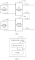
- FIG. 1 is a connection circuit diagram of a photovoltaic converter string according to the prior art.
- a first photovoltaic converter 100 and a second photovoltaic converter 200 are connected in series, and there is a voltage on an inverter side.
- series resonance generated by C 2 and L 2 causes an increase in a voltage between points C and D of the first photovoltaic converter 100 .
- the bypass diode may be short-circuited, fail, and be damaged.
- the present invention provides a photovoltaic converter string, a control method, and a system, to protect a bypass diode connected to an output end of a photovoltaic converter when the photovoltaic converter is inserted or removed.
- this application provides a photovoltaic converter string, including a plurality of photovoltaic converters, where output ends of the plurality of photovoltaic converters are connected in series, and an input end of each of the photovoltaic converters is connected to a corresponding photovoltaic module; each photovoltaic converter includes a buck/boost circuit and a controller, an output capacitor is connected between a positive output end and a negative output end of the buck/boost circuit, and both ends of the output capacitor are connected in parallel to a bypass diode; and the controller is configured to: when the buck/boost circuit is in an off state, control, to be conducted, one of switching transistors in the buck/boost circuit that are connected in parallel to the bypass diode, and control the other switching transistors in the buck/boost circuit to be cut off, so that a voltage that the bypass diode withstands is less than or equal to a breakdown voltage of the non-conducted switching transistor.
- an output voltage of the photovoltaic converter is applied to both ends of the non-conducted switching transistor in the switching transistors connected in parallel to the bypass diode, and after the output voltage of the photovoltaic converter reaches the breakdown voltage of the non-conducted switching transistor, an avalanche breakdown occurs on the non-conducted switching transistor, the switching transistor undergoing the breakdown dissipates excess energy in a form of heat, and a voltage of both ends of the bypass diode connected to a positive output end and a negative output end of the photovoltaic converter is clamped to be less than or equal to the breakdown voltage of the switching transistor.
- the voltage that the bypass diode withstands is less than or equal to the breakdown voltage of the non-conducted switching transistor, thereby preventing the bypass diode from withstanding an excessively high output voltage and preventing the bypass diode from being damaged due to an excessively high output voltage.
- the buck/boost circuit includes at least a first switching transistor, a second switching transistor, a third switching transistor, and an inductor; a first end of the first switching transistor is connected to a positive input end of the buck/boost circuit, and a second end of the first switching transistor is connected to the positive output end of the buck/boost circuit by using the inductor and the second switching transistor that are sequentially connected in series to the second end of the first switching transistor; a first end of the third switching transistor is connected to a common end of the inductor and the second switching transistor, and a second end of the third switching transistor is connected to the negative output end of the buck/boost circuit; and a negative input end of the buck/boost circuit is connected to the negative output end of the buck/boost circuit.
- the buck/boost circuit may be in a form of a buck-boost circuit, or may be a variant of a buck-boost circuit.
- a specific type of the buck/boost circuit is not limited in this embodiment of this application, provided that the buck/boost circuit can implement a boost function, a buck function, or a buck/boost function. It may be understood that the buck/boost circuit is a power conversion circuit, and can implement voltage conversion from one direct current to another.
- controller controls one switching transistor in a boost circuit in the buck/boost circuit to be conducted, and controls the other switching transistors in the buck/boost circuit to be cut off is specifically that the controller controls the second switching transistor to be conducted, and controls both the first switching transistor and the third switching transistor to be cut off; or that the controller controls the third switching transistor to be conducted, and controls both the first switching transistor and the second switching transistor to be cut off.
- a photovoltaic converter string including a plurality of photovoltaic converters, where output ends of the plurality of photovoltaic converters are connected in series, and an input end of each of the photovoltaic converters is connected to a corresponding photovoltaic module; each photovoltaic converter includes a buck/boost circuit and a controller, an output capacitor is connected between a positive output end and a negative output end of the buck/boost circuit, and both ends of the output capacitor are connected in parallel to a bypass diode; and the controller is configured to: when the buck/boost circuit is in an off state and it is determined that an output voltage of the buck/boost circuit is greater than or equal to a preset voltage, control energy of an output end of the buck/boost circuit to be reversely leaked to the correspondingly connected photovoltaic module, to reduce a voltage that the bypass diode withstands.
- the buck/boost circuit includes a first switching transistor, a second switching transistor, a third switching transistor, and an inductor; a first end of the first switching transistor is connected to a positive input end of the buck/boost circuit, and a second end of the first switching transistor is connected to the positive output end of the buck/boost circuit by using the inductor and the second switching transistor that are sequentially connected in series to the second end of the first switching transistor; a first end of the third switching transistor is connected to a common end of the inductor and the second switching transistor, and a second end of the third switching transistor is connected to a negative input end of the buck/boost circuit; and the negative input end of the buck/boost circuit is connected to the negative output end of the buck/boost circuit.
- the buck/boost circuit may be in a form of a buck-boost circuit, or may be a variant of a buck-boost circuit.
- a specific type of the buck/boost circuit is not limited in this embodiment of this application, provided that the buck/boost circuit can implement a boost function, a buck function, or a buck/boost function. It may be understood that the buck/boost circuit is a power conversion circuit, and can implement voltage conversion from one direct current to another.
- controller controls energy of an output end of the buck/boost circuit to be reversely leaked to the correspondingly connected photovoltaic module is specifically that the controller controls both the first switching transistor and the second switching transistor to be conducted and both a fifth switching transistor and the third switching transistor to be cut off.
- a channel is formed between the output end and the input end by controlling an on/off state of a switching transistor.
- the controller controls energy of an output end of the buck/boost circuit to be reversely leaked to the corresponding photovoltaic module is specifically that the controller controls the first switching transistor to be conducted, controls the second switching transistor by using a first PWM wave, and controls the third switching transistor by using a second PWM wave, where the first PWM wave and the second PWM wave are mutually complementary.
- a switching transistor is usually controlled by providing a driving pulse for a driving end of the switching transistor, in other words, is controlled by using a PWM wave.
- the controller controls energy of an output end of the buck/boost circuit to be reversely leaked to the correspondingly connected photovoltaic module is specifically that the controller controls the first switching transistor to be conducted, controls both a fifth switching transistor and the third switching transistor to be cut off, and controls the second switching transistor by using a third PWM wave.
- a method for controlling a photovoltaic converter string where the method is used to control a photovoltaic converter string, the photovoltaic converter string includes a plurality of photovoltaic converters, output ends of the plurality of photovoltaic converters are connected in series, an input end of each of the photovoltaic converters is connected to a corresponding photovoltaic module, each photovoltaic converter includes a buck/boost circuit and a controller, an output capacitor is connected between a positive output end and a negative output end of the buck/boost circuit, and both ends of the output capacitor are connected in parallel to a bypass diode; and the method includes: when the buck/boost circuit is in an off state, controlling, to be conducted, one of switching transistors in the buck/boost circuit that are connected in parallel to the bypass diode, and controlling the other switching transistors in the buck/boost circuit to be cut off, so that a voltage that the bypass diode
- an output voltage of the photovoltaic converter is applied to both ends of the non-conducted switching transistor in the switching transistors connected in parallel to the bypass diode, and after the output voltage of the photovoltaic converter reaches the breakdown voltage of the non-conducted switching transistor, an avalanche breakdown occurs on the non-conducted switching transistor, the switching transistor undergoing the breakdown dissipates excess energy in a form of heat, and a voltage of both ends of the bypass diode connected to a positive output end and a negative output end of the photovoltaic converter is clamped to be less than or equal to the breakdown voltage of the switching transistor.
- the voltage that the bypass diode withstands is less than or equal to the breakdown voltage of the non-conducted switching transistor, thereby preventing the bypass diode from withstanding an excessively high output voltage and preventing the bypass diode from being damaged due to an excessively high output voltage.
- a method for controlling a photovoltaic converter string where the method is used to control a photovoltaic converter string, the photovoltaic converter string includes a plurality of photovoltaic converters, output ends of the plurality of photovoltaic converters are connected in series, an input end of each of the photovoltaic converters is connected to a corresponding photovoltaic module, each photovoltaic converter includes a buck/boost circuit and a controller, an output capacitor is connected between a positive output end and a negative output end of the buck/boost circuit, and both ends of the output capacitor are connected in parallel to a bypass diode; and the method includes: when the buck/boost circuit is in an off state and it is determined that an output voltage of the buck/boost circuit is greater than or equal to a preset voltage, controlling energy of an output end of the buck/boost circuit to be reversely leaked to the correspondingly connected photovoltaic module, to reduce a
- energy of an output end of the photovoltaic converter may be leaked to the photovoltaic module connected to the input end, and an output voltage of the photovoltaic converter is clamped by using the photovoltaic module, so that the voltage that the bypass diode withstands is reduced.
- a photovoltaic system including the photovoltaic converter string according to the first aspect or the photovoltaic converter string according to the second aspect, and further including an inverter, where output ends of a plurality of photovoltaic converter strings are connected in parallel and connected to an input end of the inverter.
- the photovoltaic system includes the foregoing photovoltaic converter, when a bypass diode in the photovoltaic converter is protected, the entire photovoltaic system is not shut down, so that the photovoltaic system has higher operation efficiency.
- the present invention has at least the following advantages:
- one of switching transistors in a buck/boost circuit of a photovoltaic converter that are connected in parallel to the bypass diode may be controlled to be conducted, and the other switching transistors in the buck/boost circuit of the photovoltaic converter may also be controlled to be cut off.
- an output voltage of the photovoltaic converter is applied to both ends of the non-conducted switching transistor in the switching transistors connected in parallel to the bypass diode, and after the output voltage of the photovoltaic converter reaches a breakdown voltage of the non-conducted switching transistor, an avalanche breakdown occurs on the non-conducted switching transistor, the switching transistor undergoing the breakdown dissipates excess energy in a form of heat, and a voltage of both ends of the bypass diode connected to a positive output end and a negative output end of the photovoltaic converter is clamped to be less than or equal to the breakdown voltage of the switching transistor.
- the voltage that the bypass diode withstands is less than or equal to the breakdown voltage of the non-conducted switching transistor, thereby preventing the bypass diode from withstanding an excessively high output voltage and preventing the bypass diode from being damaged due to an excessively high output voltage.
- this application further provides a photovoltaic converter string.
- energy of an output end of the buck/boost circuit is controlled to be reversely leaked to a corresponding photovoltaic module, in other words, energy of an output end of a photovoltaic converter is controlled to be leaked to the photovoltaic module connected to an input end, and an output voltage of the photovoltaic converter is clamped by using the photovoltaic module, so that a voltage that a bypass diode withstands is reduced.
- FIG. 1 is a connection circuit diagram of converters according to the prior art
- FIG. 2 is a circuit diagram of a photovoltaic converter string according to Embodiment 1 of this application;
- FIG. 3 is a schematic structural diagram of a first photovoltaic converter in the photovoltaic converter string corresponding to FIG. 2 ;
- FIG. 4 a is a circuit diagram of a buck-boost circuit according to Embodiment 2 of this application;
- FIG. 4 b is a circuit diagram of another buck-boost circuit according to Embodiment 2 of this application.
- FIG. 5 is a circuit diagram of a photovoltaic converter according to Embodiment 2 of this application.
- FIG. 6 is an equivalent circuit diagram of a photovoltaic converter according to Embodiment 2 of this application.
- FIG. 7 is an equivalent circuit diagram of another photovoltaic converter according to Embodiment 2 of this application.
- FIG. 8 is a schematic structural diagram of a first photovoltaic converter in a photovoltaic converter string according to Embodiment 3 of this application;
- FIG. 9 is an equivalent circuit diagram of another photovoltaic converter according to Embodiment 4 of this application.
- FIG. 10 is an equivalent circuit diagram of still another photovoltaic converter according to Embodiment 4 of this application.
- FIG. 11 is a waveform diagram of a first PWM wave and a second PWM wave according to this application.
- FIG. 12 is a waveform diagram in which a first PWM wave and a second PWM are mutually complementary
- FIG. 13 is a waveform diagram in which a first PWM wave and a second PWM are mutually complementary and have a same duty cycle;
- FIG. 14 is an equivalent circuit diagram of still another photovoltaic converter according to Embodiment 4 of this application.
- FIG. 15 is a flowchart of a method for controlling a photovoltaic converter string according to an embodiment of this application.
- FIG. 16 is a schematic diagram of a photovoltaic system according to an embodiment of this application.
- FIG. 17 is a flowchart of another method for controlling a photovoltaic converter string according to an embodiment of this application.
- a plurality of photovoltaic converters are connected in series to form a photovoltaic converter string, and a plurality of converter strings may be connected in parallel and then connected to a large-capacity capacitor of a single-stage inverter.
- the large-capacity capacitor of the inverter stores energy and is equivalent to a voltage source
- a capacitor and an inductor at an output end of the photovoltaic converter generate series resonance, and the voltage source is used as a stepped voltage source of the series resonance.
- a voltage applied to a bypass diode is quite high and exceeds a withstand voltage of the bypass diode.
- bypass diode is damaged. Because output ends of the plurality of photovoltaic converters are connected in series, when a bypass diode of one photovoltaic converter is damaged, bypass diodes in other photovoltaic converters connected in series to the photovoltaic converter are also damaged.
- a switching transistor in a boost circuit may be controlled to be conducted, another switching transistor may be controlled to be cut off, and an output voltage of the photovoltaic converter is applied to both ends of the non-conducted switching transistor in the boost circuit.
- the output voltage reaches a breakdown voltage of the switching transistor, a breakdown occurs on the switching transistor.
- a voltage that the bypass diode withstands is restricted within a range of the breakdown voltage. In this way, the bypass diode is prevented from withstanding an excessively high output voltage, and therefore, the bypass diode is prevented from being damaged due to an excessively high output voltage.
- Embodiment 1 of this application provides a photovoltaic converter string.
- the photovoltaic converter string includes a plurality of photovoltaic converters, output ends of the plurality of photovoltaic converters are connected in series, and an input end of each of the photovoltaic converters is connected to a corresponding photovoltaic module.
- photovoltaic converters are in a one-to-one correspondence with photovoltaic modules.
- a quantity of photovoltaic converters included in the photovoltaic converter string is not specifically limited in this application.
- one inverter may correspond to one photovoltaic converter string, or one inverter may correspond to a plurality of photovoltaic converter strings. When one inverter corresponds to a plurality of photovoltaic converter strings, output ends of the plurality of photovoltaic converter strings are connected in parallel and connected to an output end of the inverter.
- a photovoltaic converter string includes at least the following two photovoltaic converters: a first photovoltaic converter and a second photovoltaic converter. “first” and “second” are merely used to distinguish between two photovoltaic converters for ease of description, and do not constitute a limitation on this application.
- FIG. 2 is a schematic structural diagram of a photovoltaic converter string according to Embodiment 1 of this application.
- the photovoltaic converter string 300 includes a first photovoltaic converter 301 a and a second photovoltaic converter 301 b .
- An input end of the first photovoltaic converter 301 a is connected to a first photovoltaic module 302 a
- an input end of the second photovoltaic converter 301 b is connected to a second photovoltaic module 302 b
- an output end of the first photovoltaic converter 301 a and an output end of the second photovoltaic converter 301 b are connected in series.
- a negative output end Va_out ⁇ of the first photovoltaic converter 301 a is connected to a positive output end Vb_out+ of the second photovoltaic converter 301 b .
- a positive output end Va_out+ of the first photovoltaic converter 301 a is used as a positive output end of the photovoltaic converter string, and a negative output end Vb_out ⁇ of the second photovoltaic converter 301 b is used as a negative output end of the photovoltaic converter string.
- first photovoltaic converter 301 a uses the first photovoltaic converter 301 a as an example for description.
- FIG. 3 is a schematic structural diagram of the first photovoltaic converter in the photovoltaic converter string corresponding to FIG. 2 .
- the first photovoltaic converter 301 a includes a buck/boost circuit 301 a 1 and a controller 302 a 2 .
- the controller 302 a 2 controls, to be conducted, one switching transistor in switching transistors in the buck/boost circuit 301 a 1 that are connected in parallel to the bypass diode, and also controls the other switching transistors in the buck/boost circuit to be cut off, so that a voltage that the bypass diode withstands is less than or equal to a breakdown voltage of the non-conducted switching transistor. It should be noted that the controller needs to complete the foregoing control process before a photovoltaic power system is started to output a voltage.
- That the buck/boost circuit is in an off state means that the controller included in the photovoltaic converter has not received a start instruction sent by a host computer, and the host computer is a controller of an inverter.
- a clamping function for the bypass diode can be implemented provided that one of the switching transistors is controlled to be conducted and the other switching transistors are controlled to be cut off. For example, if there are two switching transistors connected in parallel to the bypass diode, one switching transistor is controlled to be conducted, and the other switching transistor is controlled to be cut off, where being cut off means being non-conducted, so that the voltage that the bypass diode withstands is less than or equal to a breakdown voltage of the non-conducted switching transistor.
- the buck/boost circuit may be implemented by using a buck-boost circuit. It should be noted that the buck-boost circuit may operate in a boost mode, or may operate in a buck mode, or may operate in a buck-first and boost-next mode. A specific operation mode is not specifically limited in this embodiment of this application.
- all switching transistors in a boost circuit in the buck/boost circuit 301 a 1 are MOS field-effect transistors (MOSFET).
- one of switching transistors in a buck/boost circuit of a photovoltaic converter that are connected in parallel to the bypass diode may be controlled to be conducted, and the other switching transistors in the buck/boost circuit of the photovoltaic converter may also be controlled to be cut off.
- a switching transistor in a buck circuit is controlled to be cut off, one switching transistor that is on an output side of the buck/boost circuit and that is connected in parallel to the bypass diode is controlled to be conducted, and another switching transistor connected in parallel to the bypass diode is controlled to be cut off.
- an output voltage of the photovoltaic converter is applied to both ends of the non-conducted switching transistor on the output side, and after the output voltage of the photovoltaic converter reaches a breakdown voltage of the non-conducted switching transistor, an avalanche breakdown occurs on the non-conducted switching transistor, the switching transistor undergoing the breakdown dissipates excess energy in a form of heat, and a voltage of both ends of the bypass diode connected to a positive output end and a negative output end of the photovoltaic converter is clamped to be less than or equal to the breakdown voltage of the switching transistor.
- the voltage that the bypass diode withstands is less than or equal to the breakdown voltage of the non-conducted switching transistor, thereby preventing the bypass diode from withstanding an excessively high output voltage and preventing the bypass diode from being damaged due to an excessively high output voltage.
- a buck/boost circuit is a buck-boost circuit
- the buck-boost circuit includes at least a first switching transistor, a second switching transistor, a third switching transistor, and an inductor.
- FIG. 4 a is a circuit diagram of a buck-boost circuit according to Embodiment 2 of this application.
- the buck-boost circuit 401 includes at least a first switching transistor Q 1 , a second switching transistor Q 3 , a third switching transistor Q 4 , and a first inductor L 1 .
- the second switching transistor Q 3 and the third switching transistor Q 4 each may be a MOS field-effect transistor, and the first switching transistor Q 1 may be a MOS field-effect transistor, or may be another type of switching transistor. This is not specifically limited in this application.
- a first end of the first switching transistor Q 1 is connected to a positive input end V_in+ of the buck-boost circuit 401 , and a second end of the first switching transistor Q 1 is connected to a positive output end V_out+ of the buck-boost circuit 401 by using the first inductor L 1 and the second switching transistor Q 3 that are sequentially connected in series to the second end of the first switching transistor Q 1 .
- a first end of the third switching transistor Q 4 is connected to a common end of the first inductor L 1 and the second switching transistor Q 3 , and a second end of the third switching transistor Q 4 is connected to a negative output end V_out ⁇ of the buck-boost circuit.
- a negative input end V_in ⁇ of the buck-boost circuit 401 is connected to the negative output end V_out ⁇ of the buck-boost circuit 401 .
- the buck-boost circuit 401 may further include a fifth switching transistor. As shown in FIG. 4 b , a first end of the fifth switching transistor Q 2 is connected to a common end of the first switching transistor Q 1 and the first inductor L 1 , and a second end of the fifth switching transistor Q 2 is connected to the negative input end V_in ⁇ of the buck-boost circuit 401 .
- Switching transistors included in a boost circuit in the buck-boost circuit 401 are the second switching transistor Q 3 and the third switching transistor Q 4 .
- Switching transistors included in a buck circuit in the buck-boost circuit 401 are the first switching transistor Q 1 and the fifth switching transistor Q 2 .
- the following describes an operating principle when a photovoltaic converter in a photovoltaic converter string is a buck-boost circuit.
- FIG. 5 is a circuit diagram of a photovoltaic converter according to Embodiment 2 of this application.
- the photovoltaic converter includes a buck-boost circuit 401 and a controller.
- the controller is not shown in the figure.
- An input end of the buck-boost circuit 401 is connected to a photovoltaic module 402 . Because the photovoltaic module 402 outputs a direct current, the photovoltaic module 402 may be used as a direct current power.
- one switching transistor in a boost circuit may be controlled to be conducted, and the other switching transistors may be controlled to be cut off.
- the following describes an operating principle by conducting a second switching transistor Q 3 or a third switching transistor Q 4 in the boost circuit. A case in which the second switching transistor Q 3 is conducted and a first switching transistor Q 1 , a fifth switching transistor Q 2 , and the third switching transistor Q 4 are cut off is first described.
- controlling the second switching transistor Q 3 to be conducted means that the controller sends a drive signal to a control end of the second switching transistor Q 3 .
- the drive signal is usually a PWM wave.
- Controlling the third switching transistor Q 4 to be cut off means that the controller does not send a drive signal to a control end of the third switching transistor Q 4 .
- the third switching transistor Q 4 is non-conducted, if a voltage applied to both ends of the third switching transistor Q 4 is greater than a preset threshold, a current may also pass through the third switching transistor Q 4 .
- FIG. 6 is an equivalent circuit diagram of a photovoltaic converter according to Embodiment 2 of this application.
- the controller of the photovoltaic converter receives a start instruction sent by an inverter, in other words, before the photovoltaic converter is started and operates, the controller needs to control the second switching transistor Q 3 in the boost circuit in the buck-boost circuit to be conducted and the first switching transistor Q 1 , the fifth switching transistor Q 2 , and the third switching transistor Q 4 to be cut off.
- the circuit provided in FIG. 5 may be equivalent to that shown in FIG. 6 .
- the third switching transistor Q 4 undergoing the avalanche can dissipate energy in the series resonant circuit in a form of heat, so that the voltage between C and D is reduced to the breakdown voltage of the third switching transistor Q 4 , and a voltage that the bypass diode D 5 withstands is restricted to be less than or equal to the breakdown voltage of the third switching transistor Q 4 , thereby preventing the bypass diode D 5 from being damaged because the bypass diode D 5 withstands an excessively high output voltage.
- the following describes a case in which a controller controls a third switching transistor Q 4 in a boost circuit to be conducted and a second switching transistor Q 3 to be cut off.
- FIG. 7 is an equivalent circuit diagram of another photovoltaic converter according to Embodiment 2 of this application.
- a controller controls a third switching transistor Q 4 in a boost circuit in a buck-boost circuit to be conducted and a first switching transistor Q 1 , a fifth switching transistor Q 2 , and a second switching transistor Q 3 to be cut off.
- the circuit provided in FIG. 5 may be equivalent to that shown in FIG. 7 .
- the second switching transistor Q 3 undergoing the avalanche can dissipate energy in the series resonant circuit in a form of heat, so that the voltage between C and D is reduced to the breakdown voltage of the second switching transistor Q 3 , and a voltage that the bypass diode D 5 withstands is restricted to be less than or equal to the breakdown voltage of the second switching transistor Q 3 , thereby preventing the bypass diode D 5 from being damaged because the bypass diode D 5 withstands an excessively high output voltage.
- Embodiment 3 of this application further provides another photovoltaic converter string.
- the photovoltaic converter string includes a plurality of photovoltaic converters, output ends of the plurality of photovoltaic converters are connected in series, and an input end of each of the photovoltaic converters is connected to a corresponding photovoltaic module.
- photovoltaic converters are in a one-to-one correspondence with photovoltaic modules.
- a quantity of photovoltaic converters included in the photovoltaic converter string is not specifically limited in this application.
- one inverter may correspond to one photovoltaic converter string, or one inverter may correspond to a plurality of photovoltaic converter strings. When one inverter corresponds to a plurality of photovoltaic converter strings, output ends of the plurality of photovoltaic converter strings are connected in parallel and connected to an output end of the inverter.
- a photovoltaic converter string includes at least the following two photovoltaic converters: a first photovoltaic converter and a second photovoltaic converter. “first” and “second” are merely used to distinguish between two photovoltaic converters for ease of description, and do not constitute a limitation on this application.
- first photovoltaic converter 601 a uses the first photovoltaic converter 601 a as an example for description.
- FIG. 8 is a schematic structural diagram of a first photovoltaic converter in a photovoltaic converter string according to Embodiment 3 of this application.
- the first photovoltaic converter 601 a includes a buck-boost circuit 601 a 1 and a controller 602 a 2 .
- the controller 602 a 2 is configured to: when the buck/boost circuit is in an off state and it is determined that an output voltage of the buck-boost circuit 601 a 1 is greater than or equal to a preset voltage, control the buck-boost circuit 601 a 1 to reversely leak energy of an output end to a corresponding first photovoltaic module 602 a , and dissipate excess energy of the output end in a form of heat by using the first photovoltaic module 602 a.
- the preset voltage should be less than a breakdown voltage of the bypass diode.
- a switching transistor in the photovoltaic converter may be controlled to be conducted or cut off, so that a channel is formed between an output end and an input end.
- the buck-boost circuit may operate in a reverse buck mode, in other words, the output end of the photovoltaic converter transfers energy to the input end in a buck mode.
- a photovoltaic converter is a buck-boost circuit to describe a specific implementation of leaking energy of an output end to an input end.
- a controller is configured to: when the buck/boost circuit is in an off state and it is determined that an output voltage of the buck-boost circuit is greater than or equal to a preset voltage, control an on/off state of each switching transistor in the circuit, so that the buck-boost circuit reversely leaks energy of an output end to a photovoltaic module connected to an input end.
- the following first describes a principle in which the controller controls a first switching transistor Q 1 and a second switching transistor Q 2 to be conducted, and also controls a fifth switching transistor Q 2 and a third switching transistor Q 4 to be cut off, so that a channel is formed between the output end and the input end, and then the energy is reversely leaked.
- the controller sends a drive signal to a control end of a switching transistor to control the switching transistor to be conducted or cut off.
- the drive signal is a PWM wave
- the controller controls a switching transistor to be conducted, the controller sends a PWM wave with a duty cycle of 100% to a control end of the switching transistor; or if the controller controls a switching transistor to be cut off, the controller does not send a PWM wave to a control end of the switching transistor.
- FIG. 9 is an equivalent circuit diagram of another photovoltaic converter according to Embodiment 4 of this application.
- a controller determines that an output voltage of a buck-boost circuit 801 is greater than or equal to a preset voltage, the controller needs to control a first switching transistor Q 1 and a second switching transistor Q 3 in the buck-boost circuit 801 to be conducted, and control a fifth switching transistor Q 2 and a third switching transistor Q 4 to be cut off.
- the output voltage of the buck-boost circuit 801 may be implemented by using a voltage detection circuit.
- the voltage detection circuit sends the detected output voltage to the controller, and the controller determines whether the output voltage is greater than or equal to the preset voltage. Because the voltage detection circuit is relatively mature, details are not described herein.
- the controller determines that the voltage between the two points C and D is greater than the preset voltage, the controller controls the first switching transistor Q 1 and the second switching transistor Q 2 to be conducted, so that resonance energy of the output end is reversely leaked to a photovoltaic module 802 , and therefore, the voltage between C and D is reduced to the preset voltage.
- a voltage that the bypass diode D 5 withstands is restricted to be less than or equal to the preset voltage, thereby preventing the bypass diode D 5 from being damaged because the bypass diode D 5 withstands an excessively high output voltage.
- the controller may further control the buck-boost circuit to operate in a reverse buck mode, so that the buck-boost circuit reversely leaks the energy of the output end to the photovoltaic module.
- the following first describes a case in a first reverse buck operating mode in which a controller controls a first switching transistor Q 1 to be conducted, controls a fifth switching transistor Q 2 to be cut off, controls a second switching transistor Q 3 by using a first PWM wave, and controls a third switching transistor Q 4 by using a second PWM wave.
- Duty cycles of the first PWM wave and the second PWM wave may be the same or different. This is not specifically limited in this application.
- FIG. 10 is an equivalent circuit diagram of still another photovoltaic converter according to Embodiment 4 of this application.
- a controller determines that an output voltage of a buck-boost circuit 801 is greater than or equal to a preset voltage, the controller controls a first switching transistor Q 1 in the buck-boost circuit 801 to remain conducted, and controls a fifth switching transistor Q 2 to remain cut off, as shown in FIG. 10 .
- the controller determines that the voltage between the two points C and D is greater than the preset voltage
- the controller controls the first switching transistor Q 1 in the buck-boost circuit 801 to remain conducted, controls the fifth switching transistor Q 2 to remain cut off, controls a second switching transistor Q 3 by using a first PWM wave, and controls a third switching transistor Q 4 by using a second PWM wave
- the controller is configured to control the buck-boost circuit to operate in a reverse buck mode, so that resonance energy of the output end of the buck-boost circuit 801 is reversely leaked to a photovoltaic module 802 , and therefore, the voltage between C and D is reduced to the preset voltage.
- a voltage that the bypass diode D 5 withstands is restricted to be less than or equal to the preset voltage, thereby preventing the bypass diode D 5 from being damaged because the bypass diode D 5 withstands an excessively high output voltage.
- the controller controls the second switching transistor Q 3 and the third switching transistor Q 4 , the following case needs to be avoided:
- the two switching transistors are conducted at the same time, and consequently, there is a short circuit between a positive output end and a negative output end of the photovoltaic converter.
- a switching transistor when a PWM wave is at a high level, a switching transistor is controlled to be conducted; or when a PWM wave is at a low level, a switching transistor is controlled to be cut off.
- waveforms corresponding to the first PWM wave and the second PWM wave cannot be at a high level at the same time.
- FIG. 12 is a waveform diagram in which a first PWM wave and a second PWM are mutually complementary.
- FIG. 12 and FIG. 11 A difference between FIG. 12 and FIG. 11 lies in that the first PWM wave and the second PWM wave in FIG. 12 are mutually complementary.
- a controller controls a second switching transistor Q 3 by using the first PWM wave and controls a third switching transistor Q 4 by using the second PWM wave
- a case in which the second switching transistor Q 3 and the third switching transistor Q 4 are cut off at the same time does not occur, in other words, there is always a case in which one of the second switching transistor Q 3 and the third switching transistor Q 4 is conducted and the other one is cut off, so that resonance energy of an output end of a buck-boost circuit 801 can be reversely leaked to a photovoltaic module 802 quickly, and then a voltage between C and D is quickly reduced to a preset voltage.
- FIG. 13 is a waveform diagram in which a first PWM wave and a second PWM are mutually complementary and have a same duty cycle.
- a difference between the figure and FIG. 12 lies in that the first PWM wave and the second PWM wave in FIG. 13 are mutually complementary and have a same duty cycle of 50%.
- a controller controls a first switching transistor Q 1 to be conducted, controls both a fifth switching transistor Q 2 and a third switching transistor Q 4 to be cut off, and controls a second switching transistor Q 3 by using a third PWM wave.
- FIG. 14 is an equivalent circuit diagram of still another photovoltaic converter according to Embodiment 4 of this application.
- a controller determines that an output voltage of a buck-boost circuit 801 is greater than or equal to a preset voltage, the controller controls a first switching transistor Q 1 to be conducted, and controls both a fifth switching transistor Q 2 and a third switching transistor Q 3 to be cut off, as shown in FIG. 14 .
- the controller determines that the voltage between the two points C and D is greater than the preset voltage, the controller controls the first switching transistor Q 1 in the buck-boost circuit 801 to remain conducted, controls both the fifth switching transistor Q 2 and the third switching transistor Q 4 to be cut off, and controls a second switching transistor Q 3 by using a third PWM wave, so that the buck-boost circuit operates in a reverse buck mode.
- this embodiment of this application further provides a method for controlling a photovoltaic converter string.
- the method is used to control a photovoltaic converter string.
- the photovoltaic converter string includes a plurality of photovoltaic converters, output ends of the plurality of photovoltaic converters are connected in series, and an input end of each of the photovoltaic converters is connected to a corresponding photovoltaic module.
- a quantity of photovoltaic converters included in the photovoltaic converter string is not specifically limited in the method. In an actual distributed photovoltaic power system to which the method is applied, one inverter may correspond to one photovoltaic converter string, or one inverter may correspond to a plurality of photovoltaic converter strings.
- each photovoltaic converter When one inverter corresponds to a plurality of photovoltaic converter strings, output ends of the plurality of photovoltaic converter strings are connected in parallel and connected to an output end of the inverter. An input end of each photovoltaic converter is connected to a corresponding photovoltaic module, and each photovoltaic converter includes a buck/boost circuit and a controller.
- the method includes the following steps:
- the buck/boost circuit When the buck/boost circuit is in an off state, controlling, to be conducted, one switching transistor in switching transistors in the buck/boost circuit that are connected in parallel to a bypass diode, and controlling the other switching transistors in the buck/boost circuit to be cut off, so that a voltage that the bypass diode withstands is less than or equal to a breakdown voltage of the non-conducted switching transistor.
- a clamping function for the bypass diode can be implemented provided that one of the switching transistors is controlled to be conducted and the other switching transistors are controlled to be cut off.
- one of switching transistors in a buck/boost circuit of a photovoltaic converter that are connected in parallel to the bypass diode may be controlled to be conducted, and the other switching transistors in the buck/boost circuit of the photovoltaic converter may also be controlled to be cut off.
- a switching transistor in a buck circuit is controlled to be cut off
- one switching transistor that is on an output side of the buck/boost circuit and that is connected in parallel to the bypass diode is controlled to be conducted
- another switching transistor connected in parallel to the bypass diode is controlled to be cut off.
- an output voltage of the photovoltaic converter is applied to both ends of the non-conducted switching transistor on the output side, and after the output voltage of the photovoltaic converter reaches a breakdown voltage of the non-conducted switching transistor, an avalanche breakdown occurs on the non-conducted switching transistor, the switching transistor undergoing the breakdown dissipates excess energy in a form of heat, and a voltage of both ends of the bypass diode connected to a positive output end and a negative output end of the photovoltaic converter is clamped to be less than or equal to the breakdown voltage of the switching transistor.
- the voltage that the bypass diode withstands is less than or equal to the breakdown voltage of the non-conducted switching transistor, thereby preventing the bypass diode from withstanding an excessively high output voltage and preventing the bypass diode from being damaged due to an excessively high output voltage.
- this embodiment of this application further provides a method for controlling a photovoltaic converter string.
- FIG. 15 is a flowchart of a method for controlling a photovoltaic converter string according to an embodiment of this application.
- the method is used to control a photovoltaic converter string.
- the photovoltaic converter string includes a plurality of photovoltaic converters, output ends of the plurality of photovoltaic converters are connected in series, and an input end of each of the photovoltaic converters is connected to a corresponding photovoltaic module.
- a quantity of photovoltaic converters included in the photovoltaic converter string is not specifically limited in the method. In an actual distributed photovoltaic power system to which the method is applied, one inverter may correspond to one photovoltaic converter string, or one inverter may correspond to a plurality of photovoltaic converter strings.
- each photovoltaic converter When one inverter corresponds to a plurality of photovoltaic converter strings, output ends of the plurality of photovoltaic converter strings are connected in parallel and connected to an output end of the inverter. An input end of each photovoltaic converter is connected to a corresponding photovoltaic module, and each photovoltaic converter includes a buck/boost circuit and a controller.
- the method includes the following operations:
- S 1002 Control energy of an output end of the buck/boost circuit to be reversely leaked to the corresponding photovoltaic module.
- the method may includes the following operations:
- this application further provides a photovoltaic converter string.
- energy of an output end of the buck/boost circuit is controlled to be reversely leaked to a corresponding photovoltaic module, in other words, energy of an output end of a photovoltaic converter is controlled to be leaked to the photovoltaic module connected to an input end, and an output voltage of the photovoltaic converter is clamped by using the photovoltaic module, so that a voltage that a bypass diode withstands is reduced.
- this embodiment of this application further provides a photovoltaic system.
- the following provides detailed descriptions with reference to the accompanying drawings.
- the system includes the photovoltaic converter string described in any one of Embodiment 1 to Embodiment 4, and the system further includes an inverter.
- FIG. 16 is a schematic diagram of a photovoltaic system according to an embodiment of this application.
- the system includes the photovoltaic converter string described in any one of the foregoing embodiments, and further includes an inverter 1103 .
- a positive output end Va_out+ of a first photovoltaic converter 601 a is connected to a positive input end of the inverter 1103
- a negative output end Va_out ⁇ of a second photovoltaic converter 601 a is connected to a negative input end of the inverter 1103 .
- Each photovoltaic converter included in the system includes a buck/boost circuit and a controller.
- the controller in the system may be further configured to control, to be conducted, one of switching transistors in a buck/boost circuit of a photovoltaic converter that are connected in parallel to the bypass diode, and also control the other switching transistors in the buck/boost circuit of the photovoltaic converter to be cut off.
- a switching transistor in a buck circuit is controlled to be cut off
- one switching transistor that is on an output side of the buck/boost circuit and that is connected in parallel to the bypass diode is controlled to be conducted
- another switching transistor connected in parallel to the bypass diode is controlled to be cut off.
- an output voltage of the photovoltaic converter is applied to both ends of the non-conducted switching transistor on the output side, and after the output voltage of the photovoltaic converter reaches a breakdown voltage of the non-conducted switching transistor, an avalanche breakdown occurs on the non-conducted switching transistor, the switching transistor undergoing the breakdown dissipates excess energy in a form of heat, and a voltage of both ends of the bypass diode connected to a positive output end and a negative output end of the photovoltaic converter is clamped to be less than or equal to the breakdown voltage of the switching transistor.
- the voltage that the bypass diode withstands is less than or equal to the breakdown voltage of the non-conducted switching transistor, thereby preventing the bypass diode from withstanding an excessively high output voltage and preventing the bypass diode from being damaged due to an excessively high output voltage.
- controller in the system may be further configured to: when it is determined that an output voltage of a buck/boost circuit is greater than or equal to a preset voltage, control energy of an output end of the buck/boost circuit to be reversely leaked to a corresponding photovoltaic module, in other words, control energy of an output end of a photovoltaic converter to be leaked to the photovoltaic module connected to an input end, and an output voltage of the photovoltaic converter is clamped by using the photovoltaic module, so that a voltage that a bypass diode withstands is reduced.
- At least one means one or more, and “a plurality of” means two or more.
- the term “and/or” is used to describe an association relationship between associated objects, and indicates that three relationships may exist. For example, “A and/or B” may indicate the following three cases: Only A exists, only B exists, and both A and B exist. A and B may be singular or plural.
- the character “/” usually indicates an “or” relationship between the associated objects. “At least one of the following” or a similar expression thereof indicates any combination of the items, including any combination of one or more of the items.
- At least one of a, b, or c may indicate a, b, c, “a and b”, “a and c”, “b and c”, or “a, b, and c”, and a, b, and c”, and a, b, and c may be singular or plural.
Landscapes
- Engineering & Computer Science (AREA)
- Power Engineering (AREA)
- Dc-Dc Converters (AREA)
- Control Of Electrical Variables (AREA)
Applications Claiming Priority (1)
| Application Number | Priority Date | Filing Date | Title |
|---|---|---|---|
| PCT/CN2019/080482 WO2020198960A1 (fr) | 2019-03-29 | 2019-03-29 | Chaîne de modules de convertisseur photovoltaïque, procédé de commande et système |
Related Parent Applications (1)
| Application Number | Title | Priority Date | Filing Date |
|---|---|---|---|
| PCT/CN2019/080482 Continuation WO2020198960A1 (fr) | 2019-03-29 | 2019-03-29 | Chaîne de modules de convertisseur photovoltaïque, procédé de commande et système |
Publications (2)
| Publication Number | Publication Date |
|---|---|
| US20210328436A1 US20210328436A1 (en) | 2021-10-21 |
| US11605951B2 true US11605951B2 (en) | 2023-03-14 |
Family
ID=72664837
Family Applications (1)
| Application Number | Title | Priority Date | Filing Date |
|---|---|---|---|
| US17/362,119 Active US11605951B2 (en) | 2019-03-29 | 2021-06-29 | Photovoltaic converter string, control method, and system |
Country Status (6)
| Country | Link |
|---|---|
| US (1) | US11605951B2 (fr) |
| EP (1) | EP3859932B1 (fr) |
| JP (1) | JP7150172B2 (fr) |
| CN (1) | CN113261174B (fr) |
| AU (1) | AU2019440052B2 (fr) |
| WO (1) | WO2020198960A1 (fr) |
Families Citing this family (1)
| Publication number | Priority date | Publication date | Assignee | Title |
|---|---|---|---|---|
| US11764679B2 (en) * | 2020-01-15 | 2023-09-19 | Solaredge Technologies Ltd. | Power device |
Citations (16)
| Publication number | Priority date | Publication date | Assignee | Title |
|---|---|---|---|---|
| US20090284232A1 (en) * | 2008-05-14 | 2009-11-19 | National Semiconductor Corporation | Method and system for selecting between centralized and distributed maximum power point tracking in an energy generating system |
| DE102008059293A1 (de) | 2008-11-27 | 2010-06-02 | Manßhardt, Hans | Solar-Stromversorgung |
| JP2011507465A (ja) | 2007-12-05 | 2011-03-03 | ソラレッジ テクノロジーズ リミテッド | 分散型電力据付における安全機構、ウェークアップ方法およびシャットダウン方法 |
| US20120043818A1 (en) | 2010-08-18 | 2012-02-23 | Volterra Semiconductor Corporation | Switching Circuits For Extracting Power From An Electric Power Source And Associated Methods |
| US20120206118A1 (en) * | 2011-02-10 | 2012-08-16 | Williams Bertrand J | Dynamic Frequency and Pulse-Width Modulation of Dual-Mode Switching Power Controllers in Photovoltaic Arrays |
| US20130320778A1 (en) | 2011-02-02 | 2013-12-05 | Sma Solar Technology Ag | Protective Device for a Photovoltaic System |
| CN103701329A (zh) | 2014-01-14 | 2014-04-02 | 许昌学院 | 一种移相全桥软开关的太阳能光伏变换器 |
| JP2014128027A (ja) | 2012-12-27 | 2014-07-07 | Toshiba Corp | 駆動回路および半導体装置 |
| CN104660167A (zh) | 2015-02-25 | 2015-05-27 | 英利能源(中国)有限公司 | 一种具有功率优化器的光伏组件的el测试方法 |
| US9236743B2 (en) | 2013-07-31 | 2016-01-12 | Shehab Ahmed | Apparatus and method for voltage and current balancing in generation of output power in power generation systems |
| CN105743432A (zh) | 2015-11-19 | 2016-07-06 | 中民新能投资有限公司 | 一种光伏发电系统及其控制方法 |
| CN106787707A (zh) | 2017-02-24 | 2017-05-31 | 上海交通大学 | 内嵌储能型多模块串联式光伏直流升压变换器及应用方法 |
| CN106953525A (zh) | 2017-01-18 | 2017-07-14 | 上海交通大学 | 阻抗型多模块串联式光伏直流升压变换器 |
| CN206947565U (zh) | 2017-07-24 | 2018-01-30 | 张光宇 | 一种压缩机端子盖 |
| CN108448633A (zh) | 2018-04-28 | 2018-08-24 | 扬州大学 | 一种适合不同功率组件级联的光伏集成组件控制器 |
| US20180287484A1 (en) | 2017-03-29 | 2018-10-04 | Solaredge Technologies Ltd. | Bypass Circuit and Method to Bypass Power Modules in Power System |
Family Cites Families (5)
| Publication number | Priority date | Publication date | Assignee | Title |
|---|---|---|---|---|
| JP5574845B2 (ja) * | 2010-06-22 | 2014-08-20 | 株式会社東芝 | 電力変換装置 |
| JP6007578B2 (ja) * | 2012-05-10 | 2016-10-12 | 富士電機株式会社 | パワー半導体モジュールおよびその組立方法 |
| CN102694041A (zh) * | 2012-05-31 | 2012-09-26 | 镇江市通灵电器有限责任公司 | 一种保护光伏组件接线盒旁路二极管的方法 |
| JP7099075B2 (ja) * | 2017-08-15 | 2022-07-12 | 富士電機株式会社 | 半導体モジュール |
| CN108711842A (zh) * | 2018-08-20 | 2018-10-26 | 珠海格力电器股份有限公司 | 放电装置 |
-
2019
- 2019-03-29 AU AU2019440052A patent/AU2019440052B2/en active Active
- 2019-03-29 WO PCT/CN2019/080482 patent/WO2020198960A1/fr active Application Filing
- 2019-03-29 CN CN201980087601.1A patent/CN113261174B/zh active Active
- 2019-03-29 JP JP2021527227A patent/JP7150172B2/ja active Active
- 2019-03-29 EP EP19922952.7A patent/EP3859932B1/fr active Active
-
2021
- 2021-06-29 US US17/362,119 patent/US11605951B2/en active Active
Patent Citations (16)
| Publication number | Priority date | Publication date | Assignee | Title |
|---|---|---|---|---|
| JP2011507465A (ja) | 2007-12-05 | 2011-03-03 | ソラレッジ テクノロジーズ リミテッド | 分散型電力据付における安全機構、ウェークアップ方法およびシャットダウン方法 |
| US20090284232A1 (en) * | 2008-05-14 | 2009-11-19 | National Semiconductor Corporation | Method and system for selecting between centralized and distributed maximum power point tracking in an energy generating system |
| DE102008059293A1 (de) | 2008-11-27 | 2010-06-02 | Manßhardt, Hans | Solar-Stromversorgung |
| US20120043818A1 (en) | 2010-08-18 | 2012-02-23 | Volterra Semiconductor Corporation | Switching Circuits For Extracting Power From An Electric Power Source And Associated Methods |
| US20130320778A1 (en) | 2011-02-02 | 2013-12-05 | Sma Solar Technology Ag | Protective Device for a Photovoltaic System |
| US20120206118A1 (en) * | 2011-02-10 | 2012-08-16 | Williams Bertrand J | Dynamic Frequency and Pulse-Width Modulation of Dual-Mode Switching Power Controllers in Photovoltaic Arrays |
| JP2014128027A (ja) | 2012-12-27 | 2014-07-07 | Toshiba Corp | 駆動回路および半導体装置 |
| US9236743B2 (en) | 2013-07-31 | 2016-01-12 | Shehab Ahmed | Apparatus and method for voltage and current balancing in generation of output power in power generation systems |
| CN103701329A (zh) | 2014-01-14 | 2014-04-02 | 许昌学院 | 一种移相全桥软开关的太阳能光伏变换器 |
| CN104660167A (zh) | 2015-02-25 | 2015-05-27 | 英利能源(中国)有限公司 | 一种具有功率优化器的光伏组件的el测试方法 |
| CN105743432A (zh) | 2015-11-19 | 2016-07-06 | 中民新能投资有限公司 | 一种光伏发电系统及其控制方法 |
| CN106953525A (zh) | 2017-01-18 | 2017-07-14 | 上海交通大学 | 阻抗型多模块串联式光伏直流升压变换器 |
| CN106787707A (zh) | 2017-02-24 | 2017-05-31 | 上海交通大学 | 内嵌储能型多模块串联式光伏直流升压变换器及应用方法 |
| US20180287484A1 (en) | 2017-03-29 | 2018-10-04 | Solaredge Technologies Ltd. | Bypass Circuit and Method to Bypass Power Modules in Power System |
| CN206947565U (zh) | 2017-07-24 | 2018-01-30 | 张光宇 | 一种压缩机端子盖 |
| CN108448633A (zh) | 2018-04-28 | 2018-08-24 | 扬州大学 | 一种适合不同功率组件级联的光伏集成组件控制器 |
Also Published As
| Publication number | Publication date |
|---|---|
| CN113261174A (zh) | 2021-08-13 |
| WO2020198960A1 (fr) | 2020-10-08 |
| CN113261174B (zh) | 2024-05-17 |
| JP2022509095A (ja) | 2022-01-20 |
| EP3859932A1 (fr) | 2021-08-04 |
| EP3859932B1 (fr) | 2023-05-10 |
| EP3859932A4 (fr) | 2021-11-24 |
| JP7150172B2 (ja) | 2022-10-07 |
| US20210328436A1 (en) | 2021-10-21 |
| AU2019440052B2 (en) | 2023-11-09 |
| AU2019440052A1 (en) | 2021-05-27 |
Similar Documents
| Publication | Publication Date | Title |
|---|---|---|
| WO2019149104A1 (fr) | Circuit d'acquisition d'énergie redondant de module de puissance et son procédé de commande | |
| US8461507B2 (en) | Device system and method for coupling multiple photovoltaic arrays | |
| CN101604910B (zh) | 功率因数校正电路 | |
| US10547251B1 (en) | Method for shutdown of an active neutral point clamped converter | |
| US11005268B2 (en) | Optimizer, control method and parallel arrangement for photovoltaic system | |
| US10164539B1 (en) | Power conversion system with clamp mode switching | |
| CN101584107A (zh) | 直流电源装置和具有该直流电源装置的空气调节器 | |
| CN103944148A (zh) | 一种t型三电平逆变器的保护方法、装置及逆变电路 | |
| JP6334336B2 (ja) | 電力変換装置 | |
| US11811235B2 (en) | Inverter apparatus and power supply system | |
| US11239746B2 (en) | Two-stage converter and method for starting the same, LLC converter, and application system | |
| US11605951B2 (en) | Photovoltaic converter string, control method, and system | |
| CN1144345C (zh) | 反激同步整流dc/dc变换器保护装置 | |
| CN212323718U (zh) | 用于i型三电平apf的短路保护装置 | |
| CN111800085A (zh) | 光伏系统pid效应修复方法、装置和光伏系统 | |
| CN111585251A (zh) | 用于i型三电平apf的短路保护装置及其方法 | |
| CN117175505B (zh) | 一种储能电源逆变器驱动保护电路、方法及储能电源 | |
| Choi et al. | Development of active gate driver to reduce switching loss for inverter system | |
| US20230115497A1 (en) | Power Converter Analog Chip and Power Converter | |
| CN117458849B (zh) | 一种柔性直流换流阀子模块拓扑结构及其参数设计方法 | |
| US20230261562A1 (en) | Power conversion device and control method thereof | |
| US20230396176A1 (en) | Llc converter, control circuit, soft start method, apparatus, and chip | |
| US20230223835A1 (en) | Serial-parallel converter protection system, controller, and converter | |
| US20240079615A1 (en) | Rapid shutdown system of energy storage device | |
| US20240097615A1 (en) | Photovoltaic power generation system |
Legal Events
| Date | Code | Title | Description |
|---|---|---|---|
| AS | Assignment |
Owner name: HUAWEI TECHNOLOGIES CO., LTD., CHINA Free format text: ASSIGNMENT OF ASSIGNORS INTEREST;ASSIGNORS:GAO, YONGBING;WANG, PANPAN;JIANG, CHENGFENG;SIGNING DATES FROM 20190621 TO 20210625;REEL/FRAME:056706/0988 |
|
| FEPP | Fee payment procedure |
Free format text: ENTITY STATUS SET TO UNDISCOUNTED (ORIGINAL EVENT CODE: BIG.); ENTITY STATUS OF PATENT OWNER: LARGE ENTITY |
|
| STPP | Information on status: patent application and granting procedure in general |
Free format text: DOCKETED NEW CASE - READY FOR EXAMINATION |
|
| AS | Assignment |
Owner name: HUAWEI DIGITAL POWER TECHNOLOGIES CO., LTD., CHINA Free format text: ASSIGNMENT OF ASSIGNORS INTEREST;ASSIGNOR:HUAWEI TECHNOLOGIES CO., LTD.;REEL/FRAME:058601/0734 Effective date: 20211230 |
|
| STPP | Information on status: patent application and granting procedure in general |
Free format text: NON FINAL ACTION MAILED |
|
| STPP | Information on status: patent application and granting procedure in general |
Free format text: NOTICE OF ALLOWANCE MAILED -- APPLICATION RECEIVED IN OFFICE OF PUBLICATIONS |
|
| STCF | Information on status: patent grant |
Free format text: PATENTED CASE |
|
| CC | Certificate of correction |