EP3859932B1 - Chaîne de modules de convertisseur photovoltaïque, procédé de commande et système - Google Patents
Chaîne de modules de convertisseur photovoltaïque, procédé de commande et système Download PDFInfo
- Publication number
- EP3859932B1 EP3859932B1 EP19922952.7A EP19922952A EP3859932B1 EP 3859932 B1 EP3859932 B1 EP 3859932B1 EP 19922952 A EP19922952 A EP 19922952A EP 3859932 B1 EP3859932 B1 EP 3859932B1
- Authority
- EP
- European Patent Office
- Prior art keywords
- switching transistor
- buck
- photovoltaic
- boost circuit
- photovoltaic converter
- Prior art date
- Legal status (The legal status is an assumption and is not a legal conclusion. Google has not performed a legal analysis and makes no representation as to the accuracy of the status listed.)
- Active
Links
- 238000000034 method Methods 0.000 title claims description 35
- 230000015556 catabolic process Effects 0.000 claims description 53
- 239000003990 capacitor Substances 0.000 claims description 24
- 230000000295 complement effect Effects 0.000 claims description 8
- 238000010586 diagram Methods 0.000 description 32
- 238000006243 chemical reaction Methods 0.000 description 4
- 230000005669 field effect Effects 0.000 description 4
- 238000001514 detection method Methods 0.000 description 3
- 239000004065 semiconductor Substances 0.000 description 3
- 238000005516 engineering process Methods 0.000 description 2
- 229910044991 metal oxide Inorganic materials 0.000 description 2
- 150000004706 metal oxides Chemical class 0.000 description 2
- 238000010248 power generation Methods 0.000 description 2
- 230000000694 effects Effects 0.000 description 1
- 238000009434 installation Methods 0.000 description 1
Images


Classifications
-
- H—ELECTRICITY
- H02—GENERATION; CONVERSION OR DISTRIBUTION OF ELECTRIC POWER
- H02J—CIRCUIT ARRANGEMENTS OR SYSTEMS FOR SUPPLYING OR DISTRIBUTING ELECTRIC POWER; SYSTEMS FOR STORING ELECTRIC ENERGY
- H02J3/00—Circuit arrangements for ac mains or ac distribution networks
- H02J3/38—Arrangements for parallely feeding a single network by two or more generators, converters or transformers
- H02J3/381—Dispersed generators
-
- H—ELECTRICITY
- H02—GENERATION; CONVERSION OR DISTRIBUTION OF ELECTRIC POWER
- H02J—CIRCUIT ARRANGEMENTS OR SYSTEMS FOR SUPPLYING OR DISTRIBUTING ELECTRIC POWER; SYSTEMS FOR STORING ELECTRIC ENERGY
- H02J1/00—Circuit arrangements for dc mains or dc distribution networks
- H02J1/10—Parallel operation of dc sources
- H02J1/102—Parallel operation of dc sources being switching converters
-
- H—ELECTRICITY
- H02—GENERATION; CONVERSION OR DISTRIBUTION OF ELECTRIC POWER
- H02M—APPARATUS FOR CONVERSION BETWEEN AC AND AC, BETWEEN AC AND DC, OR BETWEEN DC AND DC, AND FOR USE WITH MAINS OR SIMILAR POWER SUPPLY SYSTEMS; CONVERSION OF DC OR AC INPUT POWER INTO SURGE OUTPUT POWER; CONTROL OR REGULATION THEREOF
- H02M1/00—Details of apparatus for conversion
- H02M1/0067—Converter structures employing plural converter units, other than for parallel operation of the units on a single load
- H02M1/0077—Plural converter units whose outputs are connected in series
-
- H—ELECTRICITY
- H02—GENERATION; CONVERSION OR DISTRIBUTION OF ELECTRIC POWER
- H02M—APPARATUS FOR CONVERSION BETWEEN AC AND AC, BETWEEN AC AND DC, OR BETWEEN DC AND DC, AND FOR USE WITH MAINS OR SIMILAR POWER SUPPLY SYSTEMS; CONVERSION OF DC OR AC INPUT POWER INTO SURGE OUTPUT POWER; CONTROL OR REGULATION THEREOF
- H02M1/00—Details of apparatus for conversion
- H02M1/32—Means for protecting converters other than automatic disconnection
-
- H—ELECTRICITY
- H02—GENERATION; CONVERSION OR DISTRIBUTION OF ELECTRIC POWER
- H02M—APPARATUS FOR CONVERSION BETWEEN AC AND AC, BETWEEN AC AND DC, OR BETWEEN DC AND DC, AND FOR USE WITH MAINS OR SIMILAR POWER SUPPLY SYSTEMS; CONVERSION OF DC OR AC INPUT POWER INTO SURGE OUTPUT POWER; CONTROL OR REGULATION THEREOF
- H02M3/00—Conversion of dc power input into dc power output
- H02M3/02—Conversion of dc power input into dc power output without intermediate conversion into ac
- H02M3/04—Conversion of dc power input into dc power output without intermediate conversion into ac by static converters
- H02M3/10—Conversion of dc power input into dc power output without intermediate conversion into ac by static converters using discharge tubes with control electrode or semiconductor devices with control electrode
- H02M3/145—Conversion of dc power input into dc power output without intermediate conversion into ac by static converters using discharge tubes with control electrode or semiconductor devices with control electrode using devices of a triode or transistor type requiring continuous application of a control signal
- H02M3/155—Conversion of dc power input into dc power output without intermediate conversion into ac by static converters using discharge tubes with control electrode or semiconductor devices with control electrode using devices of a triode or transistor type requiring continuous application of a control signal using semiconductor devices only
- H02M3/156—Conversion of dc power input into dc power output without intermediate conversion into ac by static converters using discharge tubes with control electrode or semiconductor devices with control electrode using devices of a triode or transistor type requiring continuous application of a control signal using semiconductor devices only with automatic control of output voltage or current, e.g. switching regulators
- H02M3/158—Conversion of dc power input into dc power output without intermediate conversion into ac by static converters using discharge tubes with control electrode or semiconductor devices with control electrode using devices of a triode or transistor type requiring continuous application of a control signal using semiconductor devices only with automatic control of output voltage or current, e.g. switching regulators including plural semiconductor devices as final control devices for a single load
- H02M3/1582—Buck-boost converters
-
- H—ELECTRICITY
- H02—GENERATION; CONVERSION OR DISTRIBUTION OF ELECTRIC POWER
- H02J—CIRCUIT ARRANGEMENTS OR SYSTEMS FOR SUPPLYING OR DISTRIBUTING ELECTRIC POWER; SYSTEMS FOR STORING ELECTRIC ENERGY
- H02J2300/00—Systems for supplying or distributing electric power characterised by decentralized, dispersed, or local generation
- H02J2300/20—The dispersed energy generation being of renewable origin
- H02J2300/22—The renewable source being solar energy
- H02J2300/24—The renewable source being solar energy of photovoltaic origin
- H02J2300/26—The renewable source being solar energy of photovoltaic origin involving maximum power point tracking control for photovoltaic sources
-
- Y—GENERAL TAGGING OF NEW TECHNOLOGICAL DEVELOPMENTS; GENERAL TAGGING OF CROSS-SECTIONAL TECHNOLOGIES SPANNING OVER SEVERAL SECTIONS OF THE IPC; TECHNICAL SUBJECTS COVERED BY FORMER USPC CROSS-REFERENCE ART COLLECTIONS [XRACs] AND DIGESTS
- Y02—TECHNOLOGIES OR APPLICATIONS FOR MITIGATION OR ADAPTATION AGAINST CLIMATE CHANGE
- Y02E—REDUCTION OF GREENHOUSE GAS [GHG] EMISSIONS, RELATED TO ENERGY GENERATION, TRANSMISSION OR DISTRIBUTION
- Y02E10/00—Energy generation through renewable energy sources
- Y02E10/50—Photovoltaic [PV] energy
- Y02E10/56—Power conversion systems, e.g. maximum power point trackers
Definitions
- the present invention relates to the field of photovoltaic power generation technologies, and in particular, to a photovoltaic converter string, a control method, and a system.
- Photovoltaic power generation is a technology that uses a photovoltaic effect of a semiconductor interface to convert light energy into electric energy.
- a conventional distributed photovoltaic power system mainly includes photovoltaic modules, a controller, and an inverter.
- the photovoltaic modules are connected in series to form a photovoltaic string, and the photovoltaic string is connected to an input end of the inverter.
- the photovoltaic modules are affected by factors such as different installation angles, different shades, hot spots, and inconsistent attenuation, voltage-current curves of a plurality of photovoltaic modules in a same photovoltaic string are inconsistent, in other words, a mismatch occurs between photovoltaic modules.
- each photovoltaic module in a same photovoltaic string cannot output maximum power of the photovoltaic module, and an energy yield of the entire photovoltaic system cannot reach the maximum accordingly. Therefore, to implement maximum power output, a photovoltaic converter is added to the photovoltaic system, and the photovoltaic converter can perform maximum power tracking on each photovoltaic module, so that each photovoltaic module outputs maximum power of the photovoltaic module.
- a plurality of photovoltaic converters are connected in series to form a photovoltaic converter string.
- a plurality of photovoltaic converter strings may be connected in parallel and then connected to an input end of an inverter.
- Example of such systems could be found in patent document US 2018/287484 .
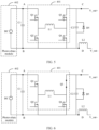
- FIG. 1 is a connection circuit diagram of a photovoltaic converter string according to the prior art.
- a first photovoltaic converter 100 and a second photovoltaic converter 200 are connected in series, and there is a voltage on an inverter side.
- series resonance generated by C2 and L2 causes an increase in a voltage between points C and D of the first photovoltaic converter 100.
- the bypass diode may be short-circuited, fail, and be damaged.
- the present invention provides a photovoltaic converter string, a control method, and a system, to protect a bypass diode connected to an output end of a photovoltaic converter when the photovoltaic converter is inserted or removed.
- this application provides a photovoltaic converter string, including a plurality of photovoltaic converters, where output ends of the plurality of photovoltaic converters are connected in series, and an input end of each of the photovoltaic converters is connected to a corresponding photovoltaic module; each photovoltaic converter includes a buck/boost circuit and a controller, an output capacitor is connected between a positive output end and a negative output end of the buck/boost circuit, and both ends of the output capacitor are connected in parallel to a bypass diode; and the controller is configured to: when the buck/boost circuit is in an off state, control, to be conducted, one of switching transistors in the buck/boost circuit that are connected in parallel to the bypass diode, and control the other switching transistors in the buck/boost circuit to be cut off, so that a voltage that the bypass diode withstands is less than or equal to a breakdown voltage of the non-conducted switching transistor.
- an output voltage of the photovoltaic converter is applied to both ends of the non-conducted switching transistor in the switching transistors connected in parallel to the bypass diode, and after the output voltage of the photovoltaic converter reaches the breakdown voltage of the non-conducted switching transistor, an avalanche breakdown occurs on the non-conducted switching transistor, the switching transistor undergoing the breakdown dissipates excess energy in a form of heat, and a voltage of both ends of the bypass diode connected to a positive output end and a negative output end of the photovoltaic converter is clamped to be less than or equal to the breakdown voltage of the switching transistor.
- the voltage that the bypass diode withstands is less than or equal to the breakdown voltage of the non-conducted switching transistor, thereby preventing the bypass diode from withstanding an excessively high output voltage and preventing the bypass diode from being damaged due to an excessively high output voltage.
- the buck/boost circuit includes at least a first switching transistor, a second switching transistor, a third switching transistor, and an inductor; a first end of the first switching transistor is connected to a positive input end of the buck/boost circuit, and a second end of the first switching transistor is connected to the positive output end of the buck/boost circuit by using the inductor and the second switching transistor that are sequentially connected in series to the second end of the first switching transistor; a first end of the third switching transistor is connected to a common end of the inductor and the second switching transistor, and a second end of the third switching transistor is connected to the negative output end of the buck/boost circuit; and a negative input end of the buck/boost circuit is connected to the negative output end of the buck/boost circuit.
- the buck/boost circuit may be in a form of a buck-boost circuit, or may be a variant of a buck-boost circuit.
- a specific type of the buck/boost circuit is not limited in this embodiment of this application, provided that the buck/boost circuit can implement a boost function, a buck function, or a buck/boost function. It may be understood that the buck/boost circuit is a power conversion circuit, and can implement voltage conversion from one direct current to another.
- controller controls one switching transistor in a boost circuit in the buck/boost circuit to be conducted, and controls the other switching transistors in the buck/boost circuit to be cut off is specifically that the controller controls the second switching transistor to be conducted, and controls both the first switching transistor and the third switching transistor to be cut off; or that the controller controls the third switching transistor to be conducted, and controls both the first switching transistor and the second switching transistor to be cut off.
- a photovoltaic converter string including a plurality of photovoltaic converters, where output ends of the plurality of photovoltaic converters are connected in series, and an input end of each of the photovoltaic converters is connected to a corresponding photovoltaic module; each photovoltaic converter includes a buck/boost circuit and a controller, an output capacitor is connected between a positive output end and a negative output end of the buck/boost circuit, and both ends of the output capacitor are connected in parallel to a bypass diode; and the controller is configured to: when the buck/boost circuit is in an off state and it is determined that an output voltage of the buck/boost circuit is greater than or equal to a preset voltage, control energy of an output end of the buck/boost circuit to be reversely leaked to the correspondingly connected photovoltaic module, to reduce a voltage that the bypass diode withstands.
- the buck/boost circuit includes a first switching transistor, a second switching transistor, a third switching transistor, and an inductor; a first end of the first switching transistor is connected to a positive input end of the buck/boost circuit, and a second end of the first switching transistor is connected to the positive output end of the buck/boost circuit by using the inductor and the second switching transistor that are sequentially connected in series to the second end of the first switching transistor; a first end of the third switching transistor is connected to a common end of the inductor and the second switching transistor, and a second end of the third switching transistor is connected to a negative input end of the buck/boost circuit; and the negative input end of the buck/boost circuit is connected to the negative output end of the buck/boost circuit.
- the buck/boost circuit may be in a form of a buck-boost circuit, or may be a variant of a buck-boost circuit.
- a specific type of the buck/boost circuit is not limited in this embodiment of this application, provided that the buck/boost circuit can implement a boost function, a buck function, or a buck/boost function. It may be understood that the buck/boost circuit is a power conversion circuit, and can implement voltage conversion from one direct current to another.
- controller controls energy of an output end of the buck/boost circuit to be reversely leaked to the correspondingly connected photovoltaic module is specifically that the controller controls both the first switching transistor and the second switching transistor to be conducted and both a fifth switching transistor and the third switching transistor to be cut off.
- a channel is formed between the output end and the input end by controlling an on/off state of a switching transistor.
- the controller controls energy of an output end of the buck/boost circuit to be reversely leaked to the corresponding photovoltaic module is specifically that the controller controls the first switching transistor to be conducted, controls the second switching transistor by using a first PWM wave, and controls the third switching transistor by using a second PWM wave, where the first PWM wave and the second PMW wave are mutually complementary.
- a switching transistor is usually controlled by providing a driving pulse for a driving end of the switching transistor, in other words, is controlled by using a PWM wave.
- the controller controls energy of an output end of the buck/boost circuit to be reversely leaked to the correspondingly connected photovoltaic module is specifically that the controller controls the first switching transistor to be conducted, controls both a fifth switching transistor and the third switching transistor to be cut off, and controls the second switching transistor by using a third PWM wave.
- a method for controlling a photovoltaic converter string where the method is used to control a photovoltaic converter string, the photovoltaic converter string includes a plurality of photovoltaic converters, output ends of the plurality of photovoltaic converters are connected in series, an input end of each of the photovoltaic converters is connected to a corresponding photovoltaic module, each photovoltaic converter includes a buck/boost circuit and a controller, an output capacitor is connected between a positive output end and a negative output end of the buck/boost circuit, and both ends of the output capacitor are connected in parallel to a bypass diode; and the method includes: when the buck/boost circuit is in an off state, controlling, to be conducted, one of switching transistors in the buck/boost circuit that are connected in parallel to the bypass diode, and controlling the other switching transistors in the buck/boost circuit to be cut off, so that a voltage that the bypass diode
- an output voltage of the photovoltaic converter is applied to both ends of the non-conducted switching transistor in the switching transistors connected in parallel to the bypass diode, and after the output voltage of the photovoltaic converter reaches the breakdown voltage of the non-conducted switching transistor, an avalanche breakdown occurs on the non-conducted switching transistor, the switching transistor undergoing the breakdown dissipates excess energy in a form of heat, and a voltage of both ends of the bypass diode connected to a positive output end and a negative output end of the photovoltaic converter is clamped to be less than or equal to the breakdown voltage of the switching transistor.
- the voltage that the bypass diode withstands is less than or equal to the breakdown voltage of the non-conducted switching transistor, thereby preventing the bypass diode from withstanding an excessively high output voltage and preventing the bypass diode from being damaged due to an excessively high output voltage.
- a method for controlling a photovoltaic converter string where the method is used to control a photovoltaic converter string, the photovoltaic converter string includes a plurality of photovoltaic converters, output ends of the plurality of photovoltaic converters are connected in series, an input end of each of the photovoltaic converters is connected to a corresponding photovoltaic module, each photovoltaic converter includes a buck/boost circuit and a controller, an output capacitor is connected between a positive output end and a negative output end of the buck/boost circuit, and both ends of the output capacitor are connected in parallel to a bypass diode; and the method includes: when the buck/boost circuit is in an off state and it is determined that an output voltage of the buck/boost circuit is greater than or equal to a preset voltage, controlling energy of an output end of the buck/boost circuit to be reversely leaked to the correspondingly connected photovoltaic module, to reduce a
- energy of an output end of the photovoltaic converter may be leaked to the photovoltaic module connected to the input end, and an output voltage of the photovoltaic converter is clamped by using the photovoltaic module, so that the voltage that the bypass diode withstands is reduced.
- a photovoltaic system including the photovoltaic converter string according to the first aspect or the photovoltaic converter string according to the second aspect, and further including an inverter, where output ends of a plurality of photovoltaic converter strings are connected in parallel and connected to an input end of the inverter.
- the photovoltaic system includes the foregoing photovoltaic converter, when a bypass diode in the photovoltaic converter is protected, the entire photovoltaic system is not shut down, so that the photovoltaic system has higher operation efficiency.
- the present invention has at least the following advantages: To prevent a bypass diode connected to an output end from being damaged when a photovoltaic converter string is connected due to a misoperation, one of switching transistors in a buck/boost circuit of a photovoltaic converter that are connected in parallel to the bypass diode may be controlled to be conducted, and the other switching transistors in the buck/boost circuit of the photovoltaic converter may also be controlled to be cut off.
- an output voltage of the photovoltaic converter is applied to both ends of the non-conducted switching transistor in the switching transistors connected in parallel to the bypass diode, and after the output voltage of the photovoltaic converter reaches a breakdown voltage of the non-conducted switching transistor, an avalanche breakdown occurs on the non-conducted switching transistor, the switching transistor undergoing the breakdown dissipates excess energy in a form of heat, and a voltage of both ends of the bypass diode connected to a positive output end and a negative output end of the photovoltaic converter is clamped to be less than or equal to the breakdown voltage of the switching transistor.
- the voltage that the bypass diode withstands is less than or equal to the breakdown voltage of the non-conducted switching transistor, thereby preventing the bypass diode from withstanding an excessively high output voltage and preventing the bypass diode from being damaged due to an excessively high output voltage.
- this application further provides a photovoltaic converter string.
- energy of an output end of the buck/boost circuit is controlled to be reversely leaked to a corresponding photovoltaic module, in other words, energy of an output end of a photovoltaic converter is controlled to be leaked to the photovoltaic module connected to an input end, and an output voltage of the photovoltaic converter is clamped by using the photovoltaic module, so that a voltage that a bypass diode withstands is reduced.
- a plurality of photovoltaic converters are connected in series to form a photovoltaic converter string, and a plurality of converter strings may be connected in parallel and then connected to a large-capacity capacitor of a single-stage inverter.
- the large-capacity capacitor of the inverter stores energy and is equivalent to a voltage source
- a capacitor and an inductor at an output end of the photovoltaic converter generate series resonance, and the voltage source is used as a stepped voltage source of the series resonance.
- a voltage applied to a bypass diode is quite high and exceeds a withstand voltage of the bypass diode.
- bypass diode is damaged. Because output ends of the plurality of photovoltaic converters are connected in series, when a bypass diode of one photovoltaic converter is damaged, bypass diodes in other photovoltaic converters connected in series to the photovoltaic converter are also damaged.
- a switching transistor in a boost circuit may be controlled to be conducted, another switching transistor may be controlled to be cut off, and an output voltage of the photovoltaic converter is applied to both ends of the non-conducted switching transistor in the boost circuit.
- the output voltage reaches a breakdown voltage of the switching transistor, a breakdown occurs on the switching transistor.
- a voltage that the bypass diode withstands is restricted within a range of the breakdown voltage. In this way, the bypass diode is prevented from withstanding an excessively high output voltage, and therefore, the bypass diode is prevented from being damaged due to an excessively high output voltage.
- Embodiment 1 of this application provides a photovoltaic converter string.
- the photovoltaic converter string includes a plurality of photovoltaic converters, output ends of the plurality of photovoltaic converters are connected in series, and an input end of each of the photovoltaic converters is connected to a corresponding photovoltaic module.
- photovoltaic converters are in a one-to-one correspondence with photovoltaic modules.
- a quantity of photovoltaic converters included in the photovoltaic converter string is not specifically limited in this application.
- one inverter may correspond to one photovoltaic converter string, or one inverter may correspond to a plurality of photovoltaic converter strings. When one inverter corresponds to a plurality of photovoltaic converter strings, output ends of the plurality of photovoltaic converter strings are connected in parallel and connected to an output end of the inverter.
- a photovoltaic converter string includes at least the following two photovoltaic converters: a first photovoltaic converter and a second photovoltaic converter.
- first and second are merely used to distinguish between two photovoltaic converters for ease of description, and do not constitute a limitation on this application.
- FIG. 2 is a schematic structural diagram of a photovoltaic converter string according to Embodiment 1 of this application.
- the photovoltaic converter string 300 includes a first photovoltaic converter 301a and a second photovoltaic converter 301b.
- An input end of the first photovoltaic converter 301a is connected to a first photovoltaic module 302a
- an input end of the second photovoltaic converter 301b is connected to a second photovoltaic module 302b
- an output end of the first photovoltaic converter 301a and an output end of the second photovoltaic converter 301b are connected in series.
- a negative output end Va_out- of the first photovoltaic converter 301a is connected to a positive output end Vb_out+ of the second photovoltaic converter 301b.
- a positive output end Va_out+ of the first photovoltaic converter 301a is used as a positive output end of the photovoltaic converter string, and a negative output end Vb_out- of the second photovoltaic converter 301b is used as a negative output end of the photovoltaic converter string.
- first photovoltaic converter 301a uses the first photovoltaic converter 301a as an example for description.
- FIG. 3 is a schematic structural diagram of the first photovoltaic converter in the photovoltaic converter string corresponding to FIG. 2 .
- the first photovoltaic converter 301a includes a buck/boost circuit 301a1 and a controller 302a2.
- the controller 302a2 controls, to be conducted, one switching transistor in switching transistors in the buck/boost circuit 301a1 that are connected in parallel to the bypass diode, and also controls the other switching transistors in the buck/boost circuit to be cut off, so that a voltage that the bypass diode withstands is less than or equal to a breakdown voltage of the non-conducted switching transistor. It should be noted that the controller needs to complete the foregoing control process before a photovoltaic power system is started to output a voltage.
- That the buck/boost circuit is in an off state means that the controller included in the photovoltaic converter has not received a start instruction sent by a host computer, and the host computer is a controller of an inverter.
- a clamping function for the bypass diode can be implemented provided that one of the switching transistors is controlled to be conducted and the other switching transistors are controlled to be cut off. For example, if there are two switching transistors connected in parallel to the bypass diode, one switching transistor is controlled to be conducted, and the other switching transistor is controlled to be cut off, where being cut off means being non-conducted, so that the voltage that the bypass diode withstands is less than or equal to a breakdown voltage of the non-conducted switching transistor.
- the buck/boost circuit may be implemented by using a buck-boost circuit. It should be noted that the buck-boost circuit may operate in a boost mode, or may operate in a buck mode, or may operate in a buck-first and boost-next mode. A specific operation mode is not specifically limited in this embodiment of this application.
- all switching transistors in a boost circuit in the buck/boost circuit 301a1 are MOS field-effect transistors (metal-oxide semiconductor, metal-oxide semiconductor field-effect transistor).
- one of switching transistors in a buck/boost circuit of a photovoltaic converter that are connected in parallel to the bypass diode may be controlled to be conducted, and the other switching transistors in the buck/boost circuit of the photovoltaic converter may also be controlled to be cut off.
- a switching transistor in a buck circuit is controlled to be cut off, one switching transistor that is on an output side of the buck/boost circuit and that is connected in parallel to the bypass diode is controlled to be conducted, and another switching transistor connected in parallel to the bypass diode is controlled to be cut off.
- an output voltage of the photovoltaic converter is applied to both ends of the non-conducted switching transistor on the output side, and after the output voltage of the photovoltaic converter reaches a breakdown voltage of the non-conducted switching transistor, an avalanche breakdown occurs on the non-conducted switching transistor, the switching transistor undergoing the breakdown dissipates excess energy in a form of heat, and a voltage of both ends of the bypass diode connected to a positive output end and a negative output end of the photovoltaic converter is clamped to be less than or equal to the breakdown voltage of the switching transistor.
- the voltage that the bypass diode withstands is less than or equal to the breakdown voltage of the non-conducted switching transistor, thereby preventing the bypass diode from withstanding an excessively high output voltage and preventing the bypass diode from being damaged due to an excessively high output voltage.
- a buck/boost circuit is a buck-boost circuit
- the buck-boost circuit includes at least a first switching transistor, a second switching transistor, a third switching transistor, and an inductor.
- FIG. 4a is a circuit diagram of a buck-boost circuit according to Embodiment 2 of this application.
- the buck-boost circuit 401 includes at least a first switching transistor Q1, a second switching transistor Q3, a third switching transistor Q4, and a first inductor L1.
- the second switching transistor Q3 and the third switching transistor Q4 each may be a MOS field-effect transistor, and the first switching transistor Q1 may be a MOS field-effect transistor, or may be another type of switching transistor. This is not specifically limited in this application.
- a first end of the first switching transistor Q1 is connected to a positive input end V_in+ of the buck-boost circuit 401, and a second end of the first switching transistor Q1 is connected to a positive output end V_out+ of the buck-boost circuit 401 by using the first inductor L1 and the second switching transistor Q3 that are sequentially connected in series to the second end of the first switching transistor Q1.
- a first end of the third switching transistor Q4 is connected to a common end of the first inductor L1 and the second switching transistor Q3, and a second end of the third switching transistor Q4 is connected to a negative output end V_out- of the buck-boost circuit.
- a negative input end V_in- of the buck-boost circuit 401 is connected to the negative output end V_out-of the buck-boost circuit 401.
- the buck-boost circuit 401 may further include a fifth switching transistor. As shown in FIG. 4b , a first end of the fifth switching transistor Q2 is connected to a common end of the first switching transistor Q1 and the first inductor L1, and a second end of the fifth switching transistor Q2 is connected to the negative input end V_in- of the buck-boost circuit 401.
- Switching transistors included in a boost circuit in the buck-boost circuit 401 are the second switching transistor Q3 and the third switching transistor Q4.
- Switching transistors included in a buck circuit in the buck-boost circuit 401 are the first switching transistor Q1 and the fifth switching transistor Q2.
- the following describes an operating principle when a photovoltaic converter in a photovoltaic converter string is a buck-boost circuit.
- FIG. 5 is a circuit diagram of a photovoltaic converter according to Embodiment 2 of this application.
- the photovoltaic converter includes a buck-boost circuit 401 and a controller.
- the controller is not shown in the figure.
- An input end of the buck-boost circuit 401 is connected to a photovoltaic module 402. Because the photovoltaic module 402 outputs a direct current, the photovoltaic module 402 may be used as a direct current power.
- one switching transistor in a boost circuit may be controlled to be conducted, and the other switching transistors may be controlled to be cut off.
- the following describes an operating principle by conducting a second switching transistor Q3 or a third switching transistor Q4 in the boost circuit. A case in which the second switching transistor Q3 is conducted and a first switching transistor Q1, a fifth switching transistor Q2, and the third switching transistor Q4 are cut off is first described.
- controlling the second switching transistor Q3 to be conducted means that the controller sends a drive signal to a control end of the second switching transistor Q3.
- the drive signal is usually a PWM wave.
- Controlling the third switching transistor Q4 to be cut off means that the controller does not send a drive signal to a control end of the third switching transistor Q4.
- FIG. 6 is an equivalent circuit diagram of a photovoltaic converter according to Embodiment 2 of this application.
- the controller of the photovoltaic converter receives a start instruction sent by an inverter, in other words, before the photovoltaic converter is started and operates, the controller needs to control the second switching transistor Q3 in the boost circuit in the buck-boost circuit to be conducted and the first switching transistor Q1, the fifth switching transistor Q2, and the third switching transistor Q4 to be cut off.
- the circuit provided in FIG. 5 may be equivalent to that shown in FIG. 6 .
- the third switching transistor Q4 undergoing the avalanche can dissipate energy in the series resonant circuit in a form of heat, so that the voltage between C and D is reduced to the breakdown voltage of the third switching transistor Q4, and a voltage that the bypass diode D5 withstands is restricted to be less than or equal to the breakdown voltage of the third switching transistor Q4, thereby preventing the bypass diode D5 from being damaged because the bypass diode D5 withstands an excessively high output voltage.
- the following describes a case in which a controller controls a third switching transistor Q4 in a boost circuit to be conducted and a second switching transistor Q3 to be cut off.
- FIG. 7 is an equivalent circuit diagram of another photovoltaic converter according to Embodiment 2 of this application.
- a controller controls a third switching transistor Q4 in a boost circuit in a buck-boost circuit to be conducted and a first switching transistor Q1, a fifth switching transistor Q2, and a second switching transistor Q3 to be cut off.
- the circuit provided in FIG. 5 may be equivalent to that shown in FIG. 7 .
- the second switching transistor Q3 undergoing the avalanche can dissipate energy in the series resonant circuit in a form of heat, so that the voltage between C and D is reduced to the breakdown voltage of the second switching transistor Q3, and a voltage that the bypass diode D5 withstands is restricted to be less than or equal to the breakdown voltage of the second switching transistor Q3, thereby preventing the bypass diode D5 from being damaged because the bypass diode D5 withstands an excessively high output voltage.
- Embodiment 3 of this application further provides another photovoltaic converter string.
- the photovoltaic converter string includes a plurality of photovoltaic converters, output ends of the plurality of photovoltaic converters are connected in series, and an input end of each of the photovoltaic converters is connected to a corresponding photovoltaic module.
- photovoltaic converters are in a one-to-one correspondence with photovoltaic modules.
- a quantity of photovoltaic converters included in the photovoltaic converter string is not specifically limited in this application.
- one inverter may correspond to one photovoltaic converter string, or one inverter may correspond to a plurality of photovoltaic converter strings. When one inverter corresponds to a plurality of photovoltaic converter strings, output ends of the plurality of photovoltaic converter strings are connected in parallel and connected to an output end of the inverter.
- a photovoltaic converter string includes at least the following two photovoltaic converters: a first photovoltaic converter and a second photovoltaic converter.
- first and second are merely used to distinguish between two photovoltaic converters for ease of description, and do not constitute a limitation on this application.
- first photovoltaic converter 601a uses the first photovoltaic converter 601a as an example for description.
- FIG. 8 is a schematic structural diagram of a first photovoltaic converter in a photovoltaic converter string according to Embodiment 3 of this application.
- the first photovoltaic converter 601a includes a buck-boost circuit 601a1 and a controller 602a2.
- the controller 602a2 is configured to: when the buck/boost circuit is in an off state and it is determined that an output voltage of the buck-boost circuit 601a1 is greater than or equal to a preset voltage, control the buck-boost circuit 601a1 to reversely leak energy of an output end to a corresponding first photovoltaic module 602a, and dissipate excess energy of the output end in a form of heat by using the first photovoltaic module 602a.
- the preset voltage should be less than a breakdown voltage of the bypass diode.
- a switching transistor in the photovoltaic converter may be controlled to be conducted or cut off, so that a channel is formed between an output end and an input end.
- the buck-boost circuit may operate in a reverse buck mode, in other words, the output end of the photovoltaic converter transfers energy to the input end in a buck mode.
- a photovoltaic converter is a buck-boost circuit to describe a specific implementation of leaking energy of an output end to an input end.
- a controller is configured to: when the buck/boost circuit is in an off state and it is determined that an output voltage of the buck-boost circuit is greater than or equal to a preset voltage, control an on/off state of each switching transistor in the circuit, so that the buck-boost circuit reversely leaks energy of an output end to a photovoltaic module connected to an input end.
- the following first describes a principle in which the controller controls a first switching transistor Q1 and a second switching transistor Q2 to be conducted, and also controls a fifth switching transistor Q2 and a third switching transistor Q4 to be cut off, so that a channel is formed between the output end and the input end, and then the energy is reversely leaked.
- the controller sends a drive signal to a control end of a switching transistor to control the switching transistor to be conducted or cut off.
- the drive signal is a PWM wave
- the controller controls a switching transistor to be conducted, the controller sends a PWM wave with a duty cycle of 100% to a control end of the switching transistor; or if the controller controls a switching transistor to be cut off, the controller does not send a PWM wave to a control end of the switching transistor.
- FIG. 9 is an equivalent circuit diagram of another photovoltaic converter according to Embodiment 4 of this application.
- a controller determines that an output voltage of a buck-boost circuit 801 is greater than or equal to a preset voltage, the controller needs to control a first switching transistor Q1 and a second switching transistor Q3 in the buck-boost circuit 801 to be conducted, and control a fifth switching transistor Q2 and a third switching transistor Q4 to be cut off.
- the output voltage of the buck-boost circuit 801 may be implemented by using a voltage detection circuit.
- the voltage detection circuit sends the detected output voltage to the controller, and the controller determines whether the output voltage is greater than or equal to the preset voltage. Because the voltage detection circuit is relatively mature, details are not described herein.
- the controller determines that the voltage between the two points C and D is greater than the preset voltage, the controller controls the first switching transistor Q1 and the second switching transistor Q2 to be conducted, so that resonance energy of the output end is reversely leaked to a photovoltaic module 802, and therefore, the voltage between C and D is reduced to the preset voltage.
- a voltage that the bypass diode D5 withstands is restricted to be less than or equal to the preset voltage, thereby preventing the bypass diode D5 from being damaged because the bypass diode D5 withstands an excessively high output voltage.
- the controller determines that the output voltage of the buck-boost circuit is greater than or equal to the preset voltage, the controller may further control the buck-boost circuit to operate in a reverse buck mode, so that the buck-boost circuit reversely leaks the energy of the output end to the photovoltaic module.
- the following first describes a case in a first reverse buck operating mode in which a controller controls a first switching transistor Q1 to be conducted, controls a fifth switching transistor Q2 to be cut off, controls a second switching transistor Q3 by using a first PWM wave, and controls a third switching transistor Q4 by using a second PWM wave.
- Duty cycles of the first PWM wave and the second PWM wave may be the same or different. This is not specifically limited in this application.
- FIG. 10 is an equivalent circuit diagram of still another photovoltaic converter according to Embodiment 4 of this application.
- a controller determines that an output voltage of a buck-boost circuit 801 is greater than or equal to a preset voltage, the controller controls a first switching transistor Q1 in the buck-boost circuit 801 to remain conducted, and controls a fifth switching transistor Q2 to remain cut off, as shown in FIG. 10 .
- the controller determines that the voltage between the two points C and D is greater than the preset voltage
- the controller controls the first switching transistor Q1 in the buck-boost circuit 801 to remain conducted, controls the fifth switching transistor Q2 to remain cut off, controls a second switching transistor Q3 by using a first PWM wave, and controls a third switching transistor Q4 by using a second PWM wave
- the controller is configured to control the buck-boost circuit to operate in a reverse buck mode, so that resonance energy of the output end of the buck-boost circuit 801 is reversely leaked to a photovoltaic module 802, and therefore, the voltage between C and D is reduced to the preset voltage.
- a voltage that the bypass diode D5 withstands is restricted to be less than or equal to the preset voltage, thereby preventing the bypass diode D5 from being damaged because the bypass diode D5 withstands an excessively high output voltage.
- the controller controls the second switching transistor Q3 and the third switching transistor Q4, the following case needs to be avoided:
- the two switching transistors are conducted at the same time, and consequently, there is a short circuit between a positive output end and a negative output end of the photovoltaic converter.
- a switching transistor when a PWM wave is at a high level, a switching transistor is controlled to be conducted; or when a PWM wave is at a low level, a switching transistor is controlled to be cut off.
- waveforms corresponding to the first PWM wave and the second PWM wave cannot be at a high level at the same time.
- FIG. 12 is a waveform diagram in which a first PWM wave and a second PWM are mutually complementary.
- a difference between FIG. 12 and FIG. 11 lies in that the first PWM wave and the second PWM wave in FIG. 12 are mutually complementary.
- a controller controls a second switching transistor Q3 by using the first PWM wave and controls a third switching transistor Q4 by using the second PWM wave
- a case in which the second switching transistor Q3 and the third switching transistor Q4 are cut off at the same time does not occur, in other words, there is always a case in which one of the second switching transistor Q3 and the third switching transistor Q4 is conducted and the other one is cut off, so that resonance energy of an output end of a buck-boost circuit 801 can be reversely leaked to a photovoltaic module 802 quickly, and then a voltage between C and D is quickly reduced to a preset voltage.
- FIG. 13 is a waveform diagram in which a first PWM wave and a second PWM are mutually complementary and have a same duty cycle.
- a difference between the figure and FIG. 12 lies in that the first PWM wave and the second PWM wave in FIG. 13 are mutually complementary and have a same duty cycle of 50%.
- a controller controls a first switching transistor Q1 to be conducted, controls both a fifth switching transistor Q2 and a third switching transistor Q4 to be cut off, and controls a second switching transistor Q3 by using a third PWM wave.
- FIG. 14 is an equivalent circuit diagram of still another photovoltaic converter according to Embodiment 2 of this application.
- a controller determines that an output voltage of a buck-boost circuit 801 is greater than or equal to a preset voltage, the controller controls a first switching transistor Q1 to be conducted, and controls both a fifth switching transistor Q2 and a third switching transistor Q3 to be cut off, as shown in FIG. 14 .
- the controller determines that the voltage between the two points C and D is greater than the preset voltage, the controller controls the first switching transistor Q1 in the buck-boost circuit 801 to remain conducted, controls both the fifth switching transistor Q2 and the third switching transistor Q4 to be cut off, and controls a second switching transistor Q3 by using a third PWM wave, so that the buck-boost circuit operates in a reverse buck mode.
- this embodiment of this application further provides a method for controlling a photovoltaic converter string.
- the method is used to control a photovoltaic converter string.
- the photovoltaic converter string includes a plurality of photovoltaic converters, output ends of the plurality of photovoltaic converters are connected in series, and an input end of each of the photovoltaic converters is connected to a corresponding photovoltaic module.
- a quantity of photovoltaic converters included in the photovoltaic converter string is not specifically limited in the method. In an actual distributed photovoltaic power system to which the method is applied, one inverter may correspond to one photovoltaic converter string, or one inverter may correspond to a plurality of photovoltaic converter strings.
- each photovoltaic converter When one inverter corresponds to a plurality of photovoltaic converter strings, output ends of the plurality of photovoltaic converter strings are connected in parallel and connected to an output end of the inverter. An input end of each photovoltaic converter is connected to a corresponding photovoltaic module, and each photovoltaic converter includes a buck/boost circuit and a controller.
- the method includes the following steps: When the buck/boost circuit is in an off state, controlling, to be conducted, one switching transistor in switching transistors in the buck/boost circuit that are connected in parallel to a bypass diode, and controlling the other switching transistors in the buck/boost circuit to be cut off, so that a voltage that the bypass diode withstands is less than or equal to a breakdown voltage of the non-conducted switching transistor.
- a clamping function for the bypass diode can be implemented provided that one of the switching transistors is controlled to be conducted and the other switching transistors are controlled to be cut off.
- one of switching transistors in a buck/boost circuit of a photovoltaic converter that are connected in parallel to the bypass diode may be controlled to be conducted, and the other switching transistors in the buck/boost circuit of the photovoltaic converter may also be controlled to be cut off.
- a switching transistor in a buck circuit is controlled to be cut off
- one switching transistor that is on an output side of the buck/boost circuit and that is connected in parallel to the bypass diode is controlled to be conducted
- another switching transistor connected in parallel to the bypass diode is controlled to be cut off.
- an output voltage of the photovoltaic converter is applied to both ends of the non-conducted switching transistor on the output side, and after the output voltage of the photovoltaic converter reaches a breakdown voltage of the non-conducted switching transistor, an avalanche breakdown occurs on the non-conducted switching transistor, the switching transistor undergoing the breakdown dissipates excess energy in a form of heat, and a voltage of both ends of the bypass diode connected to a positive output end and a negative output end of the photovoltaic converter is clamped to be less than or equal to the breakdown voltage of the switching transistor.
- the voltage that the bypass diode withstands is less than or equal to the breakdown voltage of the non-conducted switching transistor, thereby preventing the bypass diode from withstanding an excessively high output voltage and preventing the bypass diode from being damaged due to an excessively high output voltage.
- this embodiment of this application further provides a method for controlling a photovoltaic converter string.
- FIG. 15 is a flowchart of a method for controlling a photovoltaic converter string according to an embodiment of this application.
- the method is used to control a photovoltaic converter string.
- the photovoltaic converter string includes a plurality of photovoltaic converters, output ends of the plurality of photovoltaic converters are connected in series, and an input end of each of the photovoltaic converters is connected to a corresponding photovoltaic module.
- a quantity of photovoltaic converters included in the photovoltaic converter string is not specifically limited in the method. In an actual distributed photovoltaic power system to which the method is applied, one inverter may correspond to one photovoltaic converter string, or one inverter may correspond to a plurality of photovoltaic converter strings.
- each photovoltaic converter When one inverter corresponds to a plurality of photovoltaic converter strings, output ends of the plurality of photovoltaic converter strings are connected in parallel and connected to an output end of the inverter. An input end of each photovoltaic converter is connected to a corresponding photovoltaic module, and each photovoltaic converter includes a buck/boost circuit and a controller.
- the method includes the following steps: S1001: When the buck/boost circuit is in an off state, determine whether an output voltage of the buck/boost circuit is greater than or equal to a preset voltage.
- S1002 Control energy of an output end of the buck/boost circuit to be reversely leaked to the corresponding photovoltaic module.
- this application further provides a photovoltaic converter string.
- energy of an output end of the buck/boost circuit is controlled to be reversely leaked to a corresponding photovoltaic module, in other words, energy of an output end of a photovoltaic converter is controlled to be leaked to the photovoltaic module connected to an input end, and an output voltage of the photovoltaic converter is clamped by using the photovoltaic module, so that a voltage that a bypass diode withstands is reduced.
- this embodiment of this application further provides a photovoltaic system.
- the following provides detailed descriptions with reference to the accompanying drawings.
- the system includes the photovoltaic converter string described in any one of Embodiment 1 to Embodiment 4, and the system further includes an inverter.
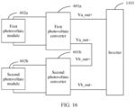
- FIG. 16 is a schematic diagram of a photovoltaic system according to an embodiment of this application.
- the system includes the photovoltaic converter string described in any one of the foregoing embodiments, and further includes an inverter 1103.
- a positive output end Va_out+ of a first photovoltaic converter 601a is connected to a positive input end of the inverter 1103, and a negative output end Va_out- of a second photovoltaic converter 601a is connected to a negative input end of the inverter 1103.
- Each photovoltaic converter included in the system includes a buck/boost circuit and a controller.
- the controller in the system may be further configured to control, to be conducted, one of switching transistors in a buck/boost circuit of a photovoltaic converter that are connected in parallel to the bypass diode, and also control the other switching transistors in the buck/boost circuit of the photovoltaic converter to be cut off.
- a switching transistor in a buck circuit is controlled to be cut off
- one switching transistor that is on an output side of the buck/boost circuit and that is connected in parallel to the bypass diode is controlled to be conducted
- another switching transistor connected in parallel to the bypass diode is controlled to be cut off.
- an output voltage of the photovoltaic converter is applied to both ends of the non-conducted switching transistor on the output side, and after the output voltage of the photovoltaic converter reaches a breakdown voltage of the non-conducted switching transistor, an avalanche breakdown occurs on the non-conducted switching transistor, the switching transistor undergoing the breakdown dissipates excess energy in a form of heat, and a voltage of both ends of the bypass diode connected to a positive output end and a negative output end of the photovoltaic converter is clamped to be less than or equal to the breakdown voltage of the switching transistor.
- the voltage that the bypass diode withstands is less than or equal to the breakdown voltage of the non-conducted switching transistor, thereby preventing the bypass diode from withstanding an excessively high output voltage and preventing the bypass diode from being damaged due to an excessively high output voltage.
- controller in the system may be further configured to: when it is determined that an output voltage of a buck/boost circuit is greater than or equal to a preset voltage, control energy of an output end of the buck/boost circuit to be reversely leaked to a corresponding photovoltaic module, in other words, control energy of an output end of a photovoltaic converter to be leaked to the photovoltaic module connected to an input end, and an output voltage of the photovoltaic converter is clamped by using the photovoltaic module, so that a voltage that a bypass diode withstands is reduced.
- At least one of a, b, or c may indicate a, b, c, "a and b", “a and c", “b and c", or "a, b, and c", and a, b, and c", and a, b, and c may be singular or plural.
Landscapes
- Engineering & Computer Science (AREA)
- Power Engineering (AREA)
- Dc-Dc Converters (AREA)
- Control Of Electrical Variables (AREA)
Claims (11)
- Chaîne de convertisseurs photovoltaïques (300), comprenant une pluralité de convertisseurs photovoltaïques (301 a, b...), dans laquelle les extrémités de sortie de la pluralité de convertisseurs photovoltaïques sont connectées en série, et une extrémité d'entrée de chacun des convertisseurs photovoltaïques est connectée à un module photovoltaïque correspondant ;chaque convertisseur photovoltaïque comprend un circuit survolteur/dévolteur et un dispositif de commande, un condensateur de sortie est connecté entre une extrémité de sortie positive et une extrémité de sortie négative du circuit survolteur/dévolteur, et les deux extrémités du condensateur de sortie sont connectées en parallèle à une diode de dérivation (D5), etle dispositif de commande est configuré pour : lorsque le dispositif de commande inclus dans le convertisseur n'a pas reçu d'instruction de démarrage, commander, pour qu'il soit allumé, l'un des transistors de commutation dans le circuit survolteur/dévolteur qui sont connectés en parallèle à la diode de dérivation, et commander les autres transistors de commutation dans le circuit survolteur/dévolteur pour qu'ils soient éteints, de sorte qu'une tension que la diode de dérivation supporte soit inférieure ou égale à une tension de claquage du transistor de commutation non allumé.
- Chaîne de convertisseurs photovoltaïques selon la revendication 1, dans laquelle le circuit survolteur/dévolteur comprend au moins un premier transistor de commutation, un deuxième transistor de commutation, un troisième transistor de commutation et un inducteur ;une première extrémité du premier transistor de commutation est connectée à une extrémité d'entrée positive du circuit survolteur/dévolteur, et une seconde extrémité du premier transistor de commutation est connectée à l'extrémité de sortie positive du circuit survolteur/dévolteur à l'aide de l'inducteur et du deuxième transistor de commutation qui sont connectés séquentiellement en série à la seconde extrémité du premier transistor de commutation ;une première extrémité du troisième transistor de commutation est connectée à une extrémité commune de l'inducteur et du deuxième transistor de commutation, et une seconde extrémité du troisième transistor de commutation est connectée à l'extrémité de sortie négative du circuit survolteur/dévolteur ; etune extrémité d'entrée négative du circuit survolteur/dévolteur est connectée à l'extrémité de sortie négative du circuit survolteur/dévolteur.
- Chaîne de convertisseurs photovoltaïques selon la revendication 2, dans laquelle le fait que le dispositif de commande commande un transistor de commutation dans un circuit survolteur dans le circuit survolteur/dévolteur pour qu'il soit allumé, et commande les autres transistors de commutation dans le circuit survolteur/dévolteur pour qu'ils soient éteints est spécifiquement :le dispositif de commande commande le deuxième transistor de commutation pour qu'il soit allumé, et commande à la fois le premier transistor de commutation et le troisième transistor de commutation pour qu'ils soient éteints ; oule dispositif de commande commande le troisième transistor de commutation pour qu'il soit allumé, et commande à la fois le premier transistor de commutation et le deuxième transistor de commutation pour qu'ils soient éteints.
- Chaîne de convertisseurs photovoltaïques, comprenant une pluralité de convertisseurs photovoltaïques (601 a, b...), dans laquelle les extrémités de sortie de la pluralité de convertisseurs photovoltaïques sont connectées en série, et une extrémité d'entrée de chacun des convertisseurs photovoltaïques est connectée à un convertisseur photovoltaïque correspondant ;chaque convertisseur photovoltaïque comprend un circuit survolteur/dévolteur et un dispositif de commande, un condensateur de sortie est connecté entre une extrémité de sortie positive et une extrémité de sortie négative du circuit survolteur/dévolteur, et les deux extrémités du condensateur de sortie sont connectées en parallèle à une diode de dérivation (D5) ; etle dispositif de commande est configuré pour : lorsque le dispositif de commande inclus dans le convertisseur n'a pas reçu d'instruction de démarrage et qu'il est déterminé qu'une tension de sortie du circuit survolteur/dévolteur est supérieure ou égale à une tension prédéfinie, commander l'énergie d'une extrémité de sortie du circuit survolteur/dévolteur de sorte qu'un canal est formé entre l'extrémité de sortie et l'extrémité d'entrée du convertisseur, pour réduire une tension que la diode de dérivation supporte.
- Chaîne de convertisseurs photovoltaïques selon la revendication 4, dans laquelle le circuit survolteur/dévolteur comprend un premier transistor de commutation, un deuxième transistor de commutation, un troisième transistor de commutation et un inducteur ;une première extrémité du premier transistor de commutation est connectée à une extrémité d'entrée positive du circuit survolteur/dévolteur, et une seconde extrémité du premier transistor de commutation est connectée à l'extrémité de sortie positive du circuit survolteur/dévolteur à l'aide de l'inducteur et du deuxième transistor de commutation qui sont connectés séquentiellement en série à la seconde extrémité du premier transistor de commutation ;une première extrémité du troisième transistor de commutation est connectée à une extrémité commune de l'inducteur et du deuxième transistor de commutation, et une seconde extrémité du troisième transistor de commutation est connectée à une extrémité d'entrée négative du circuit survolteur/dévolteur ; etl'extrémité d'entrée négative du circuit survolteur/dévolteur est connectée à l'extrémité de sortie négative du circuit survolteur/dévolteur.
- Chaîne de convertisseurs photovoltaïques selon la revendication 5, dans laquelle le fait que le dispositif de commande commande l'énergie d'une extrémité de sortie du circuit survolteur/dévolteur pour qu'elle fuie de manière inverse vers le module photovoltaïque correspondant est spécifiquement :
le dispositif de commande commande à la fois le premier transistor de commutation et le deuxième transistor de commutation pour qu'ils soient allumés et à la fois le cinquième transistor de commutation et le troisième transistor de commutation pour qu'ils soient éteints. - Chaîne de convertisseurs photovoltaïques selon la revendication 5, dans laquelle le fait que le dispositif de commande commande l'énergie d'une extrémité de sortie du circuit survolteur/dévolteur pour qu'elle fuie de manière inverse vers le module photovoltaïque connecté de manière correspondante est spécifiquement :
le dispositif de commande commande le premier transistor de commutation pour qu'il soit allumé, commande le deuxième transistor de commutation à l'aide d'une première onde MIL et commande le troisième transistor de commutation à l'aide d'une seconde onde MIL, dans laquelle la première onde MIL et la seconde onde MIL sont mutuellement complémentaires. - Chaîne de convertisseurs photovoltaïques selon la revendication 5, dans laquelle le fait que le dispositif de commande commande l'énergie d'une extrémité de sortie du circuit survolteur/dévolteur pour qu'elle fuie de manière inverse vers le module photovoltaïque connecté de manière correspondante, est spécifiquement :
le dispositif de commande commande le premier transistor de commutation pour qu'il soit allumé, commande à la fois le cinquième transistor de commutation et le troisième transistor de commutation pour qu'ils soient éteints, et commande le deuxième transistor de commutation à l'aide d'une troisième onde MIL. - Procédé pour commander une chaîne de convertisseurs photovoltaïques (300), dans lequel le procédé est utilisé pour commander une chaîne de convertisseurs photovoltaïques, la chaîne de convertisseurs photovoltaïques comprend une pluralité de convertisseurs photovoltaïques (301 a, b...), les extrémités de sortie de la pluralité des convertisseurs photovoltaïques sont connectés en série, une extrémité d'entrée de chacun des convertisseurs photovoltaïques correspond à un module photovoltaïque connecté, chaque convertisseur photovoltaïque comprend un circuit survolteur/dévolteur et un dispositif de commande, un condensateur de sortie est connecté entre une extrémité de sortie positive et une extrémité de sortie négative du circuit survolteur/dévolteur, et les deux extrémités du condensateur de sortie sont connectées en parallèle à une diode de dérivation (D5) ; et
le procédé comprend : lorsque le dispositif de commande inclus dans le convertisseur n'a pas reçu d'instruction de démarrage, la commande, pour qu'il soit allumé, de l'un des transistors de commutation dans le circuit survolteur/dévolteur qui sont connectés en parallèle à la diode de dérivation, et la commande des autres transistors de commutation dans le circuit survolteur/dévolteur pour qu'ils soient éteints, de sorte qu'une tension que la diode de dérivation supporte est inférieure ou égale à une tension de claquage du transistor de commutation non allumé. - Procédé pour commander une chaîne de convertisseurs photovoltaïques, dans lequel le procédé est utilisé pour commander une chaîne de convertisseurs photovoltaïques, la chaîne de convertisseurs photovoltaïques comprend une pluralité de convertisseurs photovoltaïques (601 a, b...), les extrémités de sortie de la pluralité de convertisseurs photovoltaïques sont connectées en série, une extrémité d'entrée de chacun des convertisseurs photovoltaïques correspond à un module photovoltaïque connecté, chaque convertisseur photovoltaïque comprend un circuit survolteur/dévolteur et un dispositif de commande, un condensateur de sortie est connecté entre une extrémité de sortie positive et une extrémité de sortie négative du circuit survolteur/dévolteur, et les deux extrémités du condensateur de sortie sont connectées en parallèle à une diode de dérivation (D5) ; et
le procédé comprend : lorsque le dispositif de commande inclus dans le convertisseur n'a pas reçu d'instruction de démarrage et qu'il est déterminé qu'une tension de sortie du circuit survolteur/dévolteur est supérieure ou égale à une tension prédéfinie, la commande de l'énergie d'une extrémité de sortie du circuit survolteur/dévolteur de telle sorte qu'un canal soit formé entre l'extrémité de sortie et l'extrémité d'entrée du convertisseur, afin de réduire une tension que la diode de dérivation supporte. - Système photovoltaïque, comprenant la chaîne de convertisseurs photovoltaïques selon l'une quelconque des revendications 1 à 3 ou la chaîne de convertisseurs photovoltaïques selon l'une quelconque des revendications 4 à 8, et comprenant en outre un onduleur, dans lequel
les extrémités de sortie de la pluralité de chaînes de convertisseurs photovoltaïques sont connectées en parallèle et connectées à une extrémité d'entrée de l'onduleur.
Applications Claiming Priority (1)
| Application Number | Priority Date | Filing Date | Title |
|---|---|---|---|
| PCT/CN2019/080482 WO2020198960A1 (fr) | 2019-03-29 | 2019-03-29 | Chaîne de modules de convertisseur photovoltaïque, procédé de commande et système |
Publications (3)
| Publication Number | Publication Date |
|---|---|
| EP3859932A1 EP3859932A1 (fr) | 2021-08-04 |
| EP3859932A4 EP3859932A4 (fr) | 2021-11-24 |
| EP3859932B1 true EP3859932B1 (fr) | 2023-05-10 |
Family
ID=72664837
Family Applications (1)
| Application Number | Title | Priority Date | Filing Date |
|---|---|---|---|
| EP19922952.7A Active EP3859932B1 (fr) | 2019-03-29 | 2019-03-29 | Chaîne de modules de convertisseur photovoltaïque, procédé de commande et système |
Country Status (6)
| Country | Link |
|---|---|
| US (1) | US11605951B2 (fr) |
| EP (1) | EP3859932B1 (fr) |
| JP (1) | JP7150172B2 (fr) |
| CN (1) | CN113261174B (fr) |
| AU (1) | AU2019440052B2 (fr) |
| WO (1) | WO2020198960A1 (fr) |
Families Citing this family (1)
| Publication number | Priority date | Publication date | Assignee | Title |
|---|---|---|---|---|
| US11764679B2 (en) * | 2020-01-15 | 2023-09-19 | Solaredge Technologies Ltd. | Power device |
Family Cites Families (21)
| Publication number | Priority date | Publication date | Assignee | Title |
|---|---|---|---|---|
| CN101933209B (zh) * | 2007-12-05 | 2015-10-21 | 太阳能安吉有限公司 | 分布式电力装置中的安全机构、醒来和关闭方法 |
| US7991511B2 (en) * | 2008-05-14 | 2011-08-02 | National Semiconductor Corporation | Method and system for selecting between centralized and distributed maximum power point tracking in an energy generating system |
| DE102008059293A1 (de) * | 2008-11-27 | 2010-06-02 | Manßhardt, Hans | Solar-Stromversorgung |
| JP5574845B2 (ja) * | 2010-06-22 | 2014-08-20 | 株式会社東芝 | 電力変換装置 |
| US9035626B2 (en) * | 2010-08-18 | 2015-05-19 | Volterra Semiconductor Corporation | Switching circuits for extracting power from an electric power source and associated methods |
| EP2671256B1 (fr) * | 2011-02-02 | 2019-03-13 | SMA Solar Technology AG | Dispositif de protection pour installation photovoltaïque |
| US8970068B2 (en) * | 2011-02-10 | 2015-03-03 | Draker, Inc. | Pseudo-random bit sequence generation for maximum power point tracking in photovoltaic arrays |
| JP6007578B2 (ja) * | 2012-05-10 | 2016-10-12 | 富士電機株式会社 | パワー半導体モジュールおよびその組立方法 |
| CN102694041A (zh) * | 2012-05-31 | 2012-09-26 | 镇江市通灵电器有限责任公司 | 一种保护光伏组件接线盒旁路二极管的方法 |
| JP6001445B2 (ja) | 2012-12-27 | 2016-10-05 | 株式会社東芝 | 駆動回路および半導体装置 |
| US9236743B2 (en) | 2013-07-31 | 2016-01-12 | Shehab Ahmed | Apparatus and method for voltage and current balancing in generation of output power in power generation systems |
| CN103701329A (zh) * | 2014-01-14 | 2014-04-02 | 许昌学院 | 一种移相全桥软开关的太阳能光伏变换器 |
| CN104660167A (zh) | 2015-02-25 | 2015-05-27 | 英利能源(中国)有限公司 | 一种具有功率优化器的光伏组件的el测试方法 |
| CN105743432B (zh) * | 2015-11-19 | 2019-04-09 | 中民新能投资集团有限公司 | 一种光伏发电系统及其控制方法 |
| CN106953525B (zh) * | 2017-01-18 | 2019-08-23 | 上海交通大学 | 阻抗型多模块串联式光伏直流升压变换器 |
| CN106787707B (zh) * | 2017-02-24 | 2020-05-22 | 上海交通大学 | 内嵌储能型多模块串联式光伏直流升压变换器及应用方法 |
| CN117175565A (zh) * | 2017-03-29 | 2023-12-05 | 太阳能安吉科技有限公司 | 旁路电路和在电力系统中旁通电力模块的方法 |
| CN206947565U (zh) | 2017-07-24 | 2018-01-30 | 张光宇 | 一种压缩机端子盖 |
| JP7099075B2 (ja) * | 2017-08-15 | 2022-07-12 | 富士電機株式会社 | 半導体モジュール |
| CN108448633B (zh) * | 2018-04-28 | 2019-12-06 | 扬州大学 | 一种适合不同功率组件级联的光伏集成组件控制器 |
| CN108711842A (zh) * | 2018-08-20 | 2018-10-26 | 珠海格力电器股份有限公司 | 放电装置 |
-
2019
- 2019-03-29 AU AU2019440052A patent/AU2019440052B2/en active Active
- 2019-03-29 WO PCT/CN2019/080482 patent/WO2020198960A1/fr active Application Filing
- 2019-03-29 CN CN201980087601.1A patent/CN113261174B/zh active Active
- 2019-03-29 JP JP2021527227A patent/JP7150172B2/ja active Active
- 2019-03-29 EP EP19922952.7A patent/EP3859932B1/fr active Active
-
2021
- 2021-06-29 US US17/362,119 patent/US11605951B2/en active Active
Also Published As
| Publication number | Publication date |
|---|---|
| CN113261174A (zh) | 2021-08-13 |
| WO2020198960A1 (fr) | 2020-10-08 |
| CN113261174B (zh) | 2024-05-17 |
| JP2022509095A (ja) | 2022-01-20 |
| EP3859932A1 (fr) | 2021-08-04 |
| EP3859932A4 (fr) | 2021-11-24 |
| JP7150172B2 (ja) | 2022-10-07 |
| US11605951B2 (en) | 2023-03-14 |
| US20210328436A1 (en) | 2021-10-21 |
| AU2019440052B2 (en) | 2023-11-09 |
| AU2019440052A1 (en) | 2021-05-27 |
Similar Documents
| Publication | Publication Date | Title |
|---|---|---|
| US8461507B2 (en) | Device system and method for coupling multiple photovoltaic arrays | |
| US9640972B2 (en) | Controlled switch-off of a power switch | |
| US7964837B2 (en) | Photovoltaic inverter interface device, system, and method | |
| US11005268B2 (en) | Optimizer, control method and parallel arrangement for photovoltaic system | |
| CN103944148A (zh) | 一种t型三电平逆变器的保护方法、装置及逆变电路 | |
| JP6334336B2 (ja) | 電力変換装置 | |
| CN101584107A (zh) | 直流电源装置和具有该直流电源装置的空气调节器 | |
| US11239746B2 (en) | Two-stage converter and method for starting the same, LLC converter, and application system | |
| US11605951B2 (en) | Photovoltaic converter string, control method, and system | |
| CN109391135B (zh) | 一种掉电保持电路以及开关电源 | |
| WO2020183700A1 (fr) | Dispositif de commande et système de génération de puissance solaire | |
| CN113938001A (zh) | 三电平变换器及其控制方法、以及供电系统 | |
| KR20130115719A (ko) | 계통연계형 멀티스트링 태양광 인버터 시스템 | |
| CN111800085A (zh) | 光伏系统pid效应修复方法、装置和光伏系统 | |
| KR102010385B1 (ko) | 전력변환장치 | |
| CN216056834U (zh) | 一种应用于电压暂降的逆变电路 | |
| US20230115497A1 (en) | Power Converter Analog Chip and Power Converter | |
| CN117175505B (zh) | 一种储能电源逆变器驱动保护电路、方法及储能电源 | |
| TWI680622B (zh) | 具有過流保護控制之換流裝置 | |
| US11545891B2 (en) | Power device and operation method thereof | |
| WO2022082769A1 (fr) | Circuit à démarrage lent à reflux d'onduleur photovoltaïque de chaîne | |
| CN117728684A (zh) | 一种功率变换器及光伏系统 | |
| KR102047868B1 (ko) | 전력 변환 장치, 그를 포함하는 에너지 저장 시스템 및 그의 구동 방법 | |
| JP2022026735A (ja) | 電力変換装置 | |
| CN114944745A (zh) | 一种变流系统及容错控制方法 |
Legal Events
| Date | Code | Title | Description |
|---|---|---|---|
| STAA | Information on the status of an ep patent application or granted ep patent |
Free format text: STATUS: THE INTERNATIONAL PUBLICATION HAS BEEN MADE |
|
| PUAI | Public reference made under article 153(3) epc to a published international application that has entered the european phase |
Free format text: ORIGINAL CODE: 0009012 |
|
| STAA | Information on the status of an ep patent application or granted ep patent |
Free format text: STATUS: REQUEST FOR EXAMINATION WAS MADE |
|
| 17P | Request for examination filed |
Effective date: 20210429 |
|
| AK | Designated contracting states |
Kind code of ref document: A1 Designated state(s): AL AT BE BG CH CY CZ DE DK EE ES FI FR GB GR HR HU IE IS IT LI LT LU LV MC MK MT NL NO PL PT RO RS SE SI SK SM TR |
|
| A4 | Supplementary search report drawn up and despatched |
Effective date: 20211021 |
|
| RIC1 | Information provided on ipc code assigned before grant |
Ipc: H02M 1/32 20070101ALI20211015BHEP Ipc: H02M 3/335 20060101ALI20211015BHEP Ipc: H02M 3/28 20060101ALI20211015BHEP Ipc: H02J 3/38 20060101AFI20211015BHEP |
|
| RAP1 | Party data changed (applicant data changed or rights of an application transferred) |
Owner name: HUAWEI DIGITAL POWER TECHNOLOGIES CO., LTD. |
|
| DAV | Request for validation of the european patent (deleted) | ||
| DAX | Request for extension of the european patent (deleted) | ||
| RIC1 | Information provided on ipc code assigned before grant |
Ipc: H02M 1/32 20070101ALI20221010BHEP Ipc: H02M 3/335 20060101ALI20221010BHEP Ipc: H02M 3/28 20060101ALI20221010BHEP Ipc: H02J 3/38 20060101AFI20221010BHEP |
|
| GRAP | Despatch of communication of intention to grant a patent |
Free format text: ORIGINAL CODE: EPIDOSNIGR1 |
|
| STAA | Information on the status of an ep patent application or granted ep patent |
Free format text: STATUS: GRANT OF PATENT IS INTENDED |
|
| INTG | Intention to grant announced |
Effective date: 20221122 |
|
| GRAS | Grant fee paid |
Free format text: ORIGINAL CODE: EPIDOSNIGR3 |
|
| GRAA | (expected) grant |
Free format text: ORIGINAL CODE: 0009210 |
|
| STAA | Information on the status of an ep patent application or granted ep patent |
Free format text: STATUS: THE PATENT HAS BEEN GRANTED |
|
| AK | Designated contracting states |
Kind code of ref document: B1 Designated state(s): AL AT BE BG CH CY CZ DE DK EE ES FI FR GB GR HR HU IE IS IT LI LT LU LV MC MK MT NL NO PL PT RO RS SE SI SK SM TR |
|
| REG | Reference to a national code |
Ref country code: GB Ref legal event code: FG4D |
|
| REG | Reference to a national code |
Ref country code: AT Ref legal event code: REF Ref document number: 1567688 Country of ref document: AT Kind code of ref document: T Effective date: 20230515 Ref country code: CH Ref legal event code: EP |
|
| REG | Reference to a national code |
Ref country code: DE Ref legal event code: R096 Ref document number: 602019028965 Country of ref document: DE |
|
| REG | Reference to a national code |
Ref country code: IE Ref legal event code: FG4D |
|
| P01 | Opt-out of the competence of the unified patent court (upc) registered |
Effective date: 20230524 |
|
| REG | Reference to a national code |
Ref country code: LT Ref legal event code: MG9D |
|
| REG | Reference to a national code |
Ref country code: NL Ref legal event code: MP Effective date: 20230510 |
|
| REG | Reference to a national code |
Ref country code: AT Ref legal event code: MK05 Ref document number: 1567688 Country of ref document: AT Kind code of ref document: T Effective date: 20230510 |
|
| PG25 | Lapsed in a contracting state [announced via postgrant information from national office to epo] |
Ref country code: SE Free format text: LAPSE BECAUSE OF FAILURE TO SUBMIT A TRANSLATION OF THE DESCRIPTION OR TO PAY THE FEE WITHIN THE PRESCRIBED TIME-LIMIT Effective date: 20230510 Ref country code: PT Free format text: LAPSE BECAUSE OF FAILURE TO SUBMIT A TRANSLATION OF THE DESCRIPTION OR TO PAY THE FEE WITHIN THE PRESCRIBED TIME-LIMIT Effective date: 20230911 Ref country code: NO Free format text: LAPSE BECAUSE OF FAILURE TO SUBMIT A TRANSLATION OF THE DESCRIPTION OR TO PAY THE FEE WITHIN THE PRESCRIBED TIME-LIMIT Effective date: 20230810 Ref country code: NL Free format text: LAPSE BECAUSE OF FAILURE TO SUBMIT A TRANSLATION OF THE DESCRIPTION OR TO PAY THE FEE WITHIN THE PRESCRIBED TIME-LIMIT Effective date: 20230510 Ref country code: ES Free format text: LAPSE BECAUSE OF FAILURE TO SUBMIT A TRANSLATION OF THE DESCRIPTION OR TO PAY THE FEE WITHIN THE PRESCRIBED TIME-LIMIT Effective date: 20230510 Ref country code: AT Free format text: LAPSE BECAUSE OF FAILURE TO SUBMIT A TRANSLATION OF THE DESCRIPTION OR TO PAY THE FEE WITHIN THE PRESCRIBED TIME-LIMIT Effective date: 20230510 |
|
| PG25 | Lapsed in a contracting state [announced via postgrant information from national office to epo] |
Ref country code: RS Free format text: LAPSE BECAUSE OF FAILURE TO SUBMIT A TRANSLATION OF THE DESCRIPTION OR TO PAY THE FEE WITHIN THE PRESCRIBED TIME-LIMIT Effective date: 20230510 Ref country code: PL Free format text: LAPSE BECAUSE OF FAILURE TO SUBMIT A TRANSLATION OF THE DESCRIPTION OR TO PAY THE FEE WITHIN THE PRESCRIBED TIME-LIMIT Effective date: 20230510 Ref country code: LV Free format text: LAPSE BECAUSE OF FAILURE TO SUBMIT A TRANSLATION OF THE DESCRIPTION OR TO PAY THE FEE WITHIN THE PRESCRIBED TIME-LIMIT Effective date: 20230510 Ref country code: LT Free format text: LAPSE BECAUSE OF FAILURE TO SUBMIT A TRANSLATION OF THE DESCRIPTION OR TO PAY THE FEE WITHIN THE PRESCRIBED TIME-LIMIT Effective date: 20230510 Ref country code: IS Free format text: LAPSE BECAUSE OF FAILURE TO SUBMIT A TRANSLATION OF THE DESCRIPTION OR TO PAY THE FEE WITHIN THE PRESCRIBED TIME-LIMIT Effective date: 20230910 Ref country code: HR Free format text: LAPSE BECAUSE OF FAILURE TO SUBMIT A TRANSLATION OF THE DESCRIPTION OR TO PAY THE FEE WITHIN THE PRESCRIBED TIME-LIMIT Effective date: 20230510 Ref country code: GR Free format text: LAPSE BECAUSE OF FAILURE TO SUBMIT A TRANSLATION OF THE DESCRIPTION OR TO PAY THE FEE WITHIN THE PRESCRIBED TIME-LIMIT Effective date: 20230811 |
|
| PG25 | Lapsed in a contracting state [announced via postgrant information from national office to epo] |
Ref country code: FI Free format text: LAPSE BECAUSE OF FAILURE TO SUBMIT A TRANSLATION OF THE DESCRIPTION OR TO PAY THE FEE WITHIN THE PRESCRIBED TIME-LIMIT Effective date: 20230510 |
|
| PG25 | Lapsed in a contracting state [announced via postgrant information from national office to epo] |
Ref country code: SK Free format text: LAPSE BECAUSE OF FAILURE TO SUBMIT A TRANSLATION OF THE DESCRIPTION OR TO PAY THE FEE WITHIN THE PRESCRIBED TIME-LIMIT Effective date: 20230510 |
|
| PG25 | Lapsed in a contracting state [announced via postgrant information from national office to epo] |
Ref country code: SM Free format text: LAPSE BECAUSE OF FAILURE TO SUBMIT A TRANSLATION OF THE DESCRIPTION OR TO PAY THE FEE WITHIN THE PRESCRIBED TIME-LIMIT Effective date: 20230510 Ref country code: SK Free format text: LAPSE BECAUSE OF FAILURE TO SUBMIT A TRANSLATION OF THE DESCRIPTION OR TO PAY THE FEE WITHIN THE PRESCRIBED TIME-LIMIT Effective date: 20230510 Ref country code: RO Free format text: LAPSE BECAUSE OF FAILURE TO SUBMIT A TRANSLATION OF THE DESCRIPTION OR TO PAY THE FEE WITHIN THE PRESCRIBED TIME-LIMIT Effective date: 20230510 Ref country code: EE Free format text: LAPSE BECAUSE OF FAILURE TO SUBMIT A TRANSLATION OF THE DESCRIPTION OR TO PAY THE FEE WITHIN THE PRESCRIBED TIME-LIMIT Effective date: 20230510 Ref country code: DK Free format text: LAPSE BECAUSE OF FAILURE TO SUBMIT A TRANSLATION OF THE DESCRIPTION OR TO PAY THE FEE WITHIN THE PRESCRIBED TIME-LIMIT Effective date: 20230510 Ref country code: CZ Free format text: LAPSE BECAUSE OF FAILURE TO SUBMIT A TRANSLATION OF THE DESCRIPTION OR TO PAY THE FEE WITHIN THE PRESCRIBED TIME-LIMIT Effective date: 20230510 |
|
| REG | Reference to a national code |
Ref country code: DE Ref legal event code: R097 Ref document number: 602019028965 Country of ref document: DE |
|
| PLBE | No opposition filed within time limit |
Free format text: ORIGINAL CODE: 0009261 |
|
| STAA | Information on the status of an ep patent application or granted ep patent |
Free format text: STATUS: NO OPPOSITION FILED WITHIN TIME LIMIT |
|
| 26N | No opposition filed |
Effective date: 20240213 |
|
| PGFP | Annual fee paid to national office [announced via postgrant information from national office to epo] |
Ref country code: DE Payment date: 20240130 Year of fee payment: 6 |
|
| PG25 | Lapsed in a contracting state [announced via postgrant information from national office to epo] |
Ref country code: SI Free format text: LAPSE BECAUSE OF FAILURE TO SUBMIT A TRANSLATION OF THE DESCRIPTION OR TO PAY THE FEE WITHIN THE PRESCRIBED TIME-LIMIT Effective date: 20230510 |