US11355469B2 - Connection structure and method for producing same - Google Patents
Connection structure and method for producing same Download PDFInfo
- Publication number
- US11355469B2 US11355469B2 US16/957,568 US201816957568A US11355469B2 US 11355469 B2 US11355469 B2 US 11355469B2 US 201816957568 A US201816957568 A US 201816957568A US 11355469 B2 US11355469 B2 US 11355469B2
- Authority
- US
- United States
- Prior art keywords
- electrode
- electronic member
- substrate
- conductive
- conductive particle
- Prior art date
- Legal status (The legal status is an assumption and is not a legal conclusion. Google has not performed a legal analysis and makes no representation as to the accuracy of the status listed.)
- Active
Links
Images


Classifications
-
- H—ELECTRICITY
- H10—SEMICONDUCTOR DEVICES; ELECTRIC SOLID-STATE DEVICES NOT OTHERWISE PROVIDED FOR
- H10W—GENERIC PACKAGES, INTERCONNECTIONS, CONNECTORS OR OTHER CONSTRUCTIONAL DETAILS OF DEVICES COVERED BY CLASS H10
- H10W72/00—Interconnections or connectors in packages
- H10W72/071—Connecting or disconnecting
- H10W72/073—Connecting or disconnecting of die-attach connectors
-
- H—ELECTRICITY
- H01—ELECTRIC ELEMENTS
- H01R—ELECTRICALLY-CONDUCTIVE CONNECTIONS; STRUCTURAL ASSOCIATIONS OF A PLURALITY OF MUTUALLY-INSULATED ELECTRICAL CONNECTING ELEMENTS; COUPLING DEVICES; CURRENT COLLECTORS
- H01R11/00—Individual connecting elements providing two or more spaced connecting locations for conductive members which are, or may be, thereby interconnected, e.g. end pieces for wires or cables supported by the wire or cable and having means for facilitating electrical connection to some other wire, terminal, or conductive member, blocks of binding posts
- H01R11/01—Individual connecting elements providing two or more spaced connecting locations for conductive members which are, or may be, thereby interconnected, e.g. end pieces for wires or cables supported by the wire or cable and having means for facilitating electrical connection to some other wire, terminal, or conductive member, blocks of binding posts characterised by the form or arrangement of the conductive interconnection between the connecting locations
-
- H01L24/32—
-
- H—ELECTRICITY
- H10—SEMICONDUCTOR DEVICES; ELECTRIC SOLID-STATE DEVICES NOT OTHERWISE PROVIDED FOR
- H10W—GENERIC PACKAGES, INTERCONNECTIONS, CONNECTORS OR OTHER CONSTRUCTIONAL DETAILS OF DEVICES COVERED BY CLASS H10
- H10W72/00—Interconnections or connectors in packages
- H10W72/30—Die-attach connectors
-
- C—CHEMISTRY; METALLURGY
- C09—DYES; PAINTS; POLISHES; NATURAL RESINS; ADHESIVES; COMPOSITIONS NOT OTHERWISE PROVIDED FOR; APPLICATIONS OF MATERIALS NOT OTHERWISE PROVIDED FOR
- C09J—ADHESIVES; NON-MECHANICAL ASPECTS OF ADHESIVE PROCESSES IN GENERAL; ADHESIVE PROCESSES NOT PROVIDED FOR ELSEWHERE; USE OF MATERIALS AS ADHESIVES
- C09J11/00—Features of adhesives not provided for in group C09J9/00, e.g. additives
- C09J11/02—Non-macromolecular additives
- C09J11/04—Non-macromolecular additives inorganic
-
- C—CHEMISTRY; METALLURGY
- C09—DYES; PAINTS; POLISHES; NATURAL RESINS; ADHESIVES; COMPOSITIONS NOT OTHERWISE PROVIDED FOR; APPLICATIONS OF MATERIALS NOT OTHERWISE PROVIDED FOR
- C09J—ADHESIVES; NON-MECHANICAL ASPECTS OF ADHESIVE PROCESSES IN GENERAL; ADHESIVE PROCESSES NOT PROVIDED FOR ELSEWHERE; USE OF MATERIALS AS ADHESIVES
- C09J201/00—Adhesives based on unspecified macromolecular compounds
-
- C—CHEMISTRY; METALLURGY
- C09—DYES; PAINTS; POLISHES; NATURAL RESINS; ADHESIVES; COMPOSITIONS NOT OTHERWISE PROVIDED FOR; APPLICATIONS OF MATERIALS NOT OTHERWISE PROVIDED FOR
- C09J—ADHESIVES; NON-MECHANICAL ASPECTS OF ADHESIVE PROCESSES IN GENERAL; ADHESIVE PROCESSES NOT PROVIDED FOR ELSEWHERE; USE OF MATERIALS AS ADHESIVES
- C09J7/00—Adhesives in the form of films or foils
-
- C—CHEMISTRY; METALLURGY
- C09—DYES; PAINTS; POLISHES; NATURAL RESINS; ADHESIVES; COMPOSITIONS NOT OTHERWISE PROVIDED FOR; APPLICATIONS OF MATERIALS NOT OTHERWISE PROVIDED FOR
- C09J—ADHESIVES; NON-MECHANICAL ASPECTS OF ADHESIVE PROCESSES IN GENERAL; ADHESIVE PROCESSES NOT PROVIDED FOR ELSEWHERE; USE OF MATERIALS AS ADHESIVES
- C09J9/00—Adhesives characterised by their physical nature or the effects produced, e.g. glue sticks
- C09J9/02—Electrically-conducting adhesives
-
- H01L24/29—
-
- H—ELECTRICITY
- H01—ELECTRIC ELEMENTS
- H01R—ELECTRICALLY-CONDUCTIVE CONNECTIONS; STRUCTURAL ASSOCIATIONS OF A PLURALITY OF MUTUALLY-INSULATED ELECTRICAL CONNECTING ELEMENTS; COUPLING DEVICES; CURRENT COLLECTORS
- H01R43/00—Apparatus or processes specially adapted for manufacturing, assembling, maintaining, or repairing of line connectors or current collectors or for joining electric conductors
-
- H—ELECTRICITY
- H05—ELECTRIC TECHNIQUES NOT OTHERWISE PROVIDED FOR
- H05K—PRINTED CIRCUITS; CASINGS OR CONSTRUCTIONAL DETAILS OF ELECTRIC APPARATUS; MANUFACTURE OF ASSEMBLAGES OF ELECTRICAL COMPONENTS
- H05K1/00—Printed circuits
- H05K1/02—Details
- H05K1/14—Structural association of two or more printed circuits
-
- H—ELECTRICITY
- H05—ELECTRIC TECHNIQUES NOT OTHERWISE PROVIDED FOR
- H05K—PRINTED CIRCUITS; CASINGS OR CONSTRUCTIONAL DETAILS OF ELECTRIC APPARATUS; MANUFACTURE OF ASSEMBLAGES OF ELECTRICAL COMPONENTS
- H05K3/00—Apparatus or processes for manufacturing printed circuits
- H05K3/30—Assembling printed circuits with electric components, e.g. with resistors
- H05K3/32—Assembling printed circuits with electric components, e.g. with resistors electrically connecting electric components or wires to printed circuits
- H05K3/321—Assembling printed circuits with electric components, e.g. with resistors electrically connecting electric components or wires to printed circuits by conductive adhesives
- H05K3/323—Assembling printed circuits with electric components, e.g. with resistors electrically connecting electric components or wires to printed circuits by conductive adhesives by applying an anisotropic conductive adhesive layer over an array of pads
-
- H—ELECTRICITY
- H05—ELECTRIC TECHNIQUES NOT OTHERWISE PROVIDED FOR
- H05K—PRINTED CIRCUITS; CASINGS OR CONSTRUCTIONAL DETAILS OF ELECTRIC APPARATUS; MANUFACTURE OF ASSEMBLAGES OF ELECTRICAL COMPONENTS
- H05K3/00—Apparatus or processes for manufacturing printed circuits
- H05K3/36—Assembling printed circuits with other printed circuits
- H05K3/361—Assembling flexible printed circuits with other printed circuits
-
- H01L2224/29144—
-
- H01L2224/29155—
-
- H01L2224/29164—
-
- H01L2224/32145—
-
- H—ELECTRICITY
- H10—SEMICONDUCTOR DEVICES; ELECTRIC SOLID-STATE DEVICES NOT OTHERWISE PROVIDED FOR
- H10W—GENERIC PACKAGES, INTERCONNECTIONS, CONNECTORS OR OTHER CONSTRUCTIONAL DETAILS OF DEVICES COVERED BY CLASS H10
- H10W72/00—Interconnections or connectors in packages
- H10W72/01—Manufacture or treatment
- H10W72/013—Manufacture or treatment of die-attach connectors
- H10W72/01331—Manufacture or treatment of die-attach connectors using blanket deposition
- H10W72/01333—Manufacture or treatment of die-attach connectors using blanket deposition in liquid form, e.g. spin coating, spray coating or immersion coating
-
- H—ELECTRICITY
- H10—SEMICONDUCTOR DEVICES; ELECTRIC SOLID-STATE DEVICES NOT OTHERWISE PROVIDED FOR
- H10W—GENERIC PACKAGES, INTERCONNECTIONS, CONNECTORS OR OTHER CONSTRUCTIONAL DETAILS OF DEVICES COVERED BY CLASS H10
- H10W72/00—Interconnections or connectors in packages
- H10W72/071—Connecting or disconnecting
- H10W72/073—Connecting or disconnecting of die-attach connectors
- H10W72/07331—Connecting techniques
- H10W72/07332—Compression bonding, e.g. thermocompression bonding
-
- H—ELECTRICITY
- H10—SEMICONDUCTOR DEVICES; ELECTRIC SOLID-STATE DEVICES NOT OTHERWISE PROVIDED FOR
- H10W—GENERIC PACKAGES, INTERCONNECTIONS, CONNECTORS OR OTHER CONSTRUCTIONAL DETAILS OF DEVICES COVERED BY CLASS H10
- H10W72/00—Interconnections or connectors in packages
- H10W72/071—Connecting or disconnecting
- H10W72/073—Connecting or disconnecting of die-attach connectors
- H10W72/07331—Connecting techniques
- H10W72/07337—Connecting techniques using a polymer adhesive, e.g. an adhesive based on silicone or epoxy
- H10W72/07338—Connecting techniques using a polymer adhesive, e.g. an adhesive based on silicone or epoxy hardening the adhesive by curing, e.g. thermosetting
-
- H—ELECTRICITY
- H10—SEMICONDUCTOR DEVICES; ELECTRIC SOLID-STATE DEVICES NOT OTHERWISE PROVIDED FOR
- H10W—GENERIC PACKAGES, INTERCONNECTIONS, CONNECTORS OR OTHER CONSTRUCTIONAL DETAILS OF DEVICES COVERED BY CLASS H10
- H10W72/00—Interconnections or connectors in packages
- H10W72/071—Connecting or disconnecting
- H10W72/073—Connecting or disconnecting of die-attach connectors
- H10W72/07351—Connecting or disconnecting of die-attach connectors characterised by changes in properties of the die-attach connectors during connecting
- H10W72/07353—Connecting or disconnecting of die-attach connectors characterised by changes in properties of the die-attach connectors during connecting changes in shapes
-
- H—ELECTRICITY
- H10—SEMICONDUCTOR DEVICES; ELECTRIC SOLID-STATE DEVICES NOT OTHERWISE PROVIDED FOR
- H10W—GENERIC PACKAGES, INTERCONNECTIONS, CONNECTORS OR OTHER CONSTRUCTIONAL DETAILS OF DEVICES COVERED BY CLASS H10
- H10W72/00—Interconnections or connectors in packages
- H10W72/071—Connecting or disconnecting
- H10W72/074—Connecting or disconnecting of anisotropic conductive adhesives
-
- H—ELECTRICITY
- H10—SEMICONDUCTOR DEVICES; ELECTRIC SOLID-STATE DEVICES NOT OTHERWISE PROVIDED FOR
- H10W—GENERIC PACKAGES, INTERCONNECTIONS, CONNECTORS OR OTHER CONSTRUCTIONAL DETAILS OF DEVICES COVERED BY CLASS H10
- H10W72/00—Interconnections or connectors in packages
- H10W72/30—Die-attach connectors
- H10W72/321—Structures or relative sizes of die-attach connectors
- H10W72/325—Die-attach connectors having a filler embedded in a matrix
-
- H—ELECTRICITY
- H10—SEMICONDUCTOR DEVICES; ELECTRIC SOLID-STATE DEVICES NOT OTHERWISE PROVIDED FOR
- H10W—GENERIC PACKAGES, INTERCONNECTIONS, CONNECTORS OR OTHER CONSTRUCTIONAL DETAILS OF DEVICES COVERED BY CLASS H10
- H10W72/00—Interconnections or connectors in packages
- H10W72/30—Die-attach connectors
- H10W72/331—Shapes of die-attach connectors
-
- H—ELECTRICITY
- H10—SEMICONDUCTOR DEVICES; ELECTRIC SOLID-STATE DEVICES NOT OTHERWISE PROVIDED FOR
- H10W—GENERIC PACKAGES, INTERCONNECTIONS, CONNECTORS OR OTHER CONSTRUCTIONAL DETAILS OF DEVICES COVERED BY CLASS H10
- H10W72/00—Interconnections or connectors in packages
- H10W72/30—Die-attach connectors
- H10W72/351—Materials of die-attach connectors
- H10W72/352—Materials of die-attach connectors comprising metals or metalloids, e.g. solders
-
- H—ELECTRICITY
- H10—SEMICONDUCTOR DEVICES; ELECTRIC SOLID-STATE DEVICES NOT OTHERWISE PROVIDED FOR
- H10W—GENERIC PACKAGES, INTERCONNECTIONS, CONNECTORS OR OTHER CONSTRUCTIONAL DETAILS OF DEVICES COVERED BY CLASS H10
- H10W72/00—Interconnections or connectors in packages
- H10W72/30—Die-attach connectors
- H10W72/351—Materials of die-attach connectors
- H10W72/353—Materials of die-attach connectors not comprising solid metals or solid metalloids, e.g. ceramics
- H10W72/354—Materials of die-attach connectors not comprising solid metals or solid metalloids, e.g. ceramics comprising polymers
-
- H—ELECTRICITY
- H10—SEMICONDUCTOR DEVICES; ELECTRIC SOLID-STATE DEVICES NOT OTHERWISE PROVIDED FOR
- H10W—GENERIC PACKAGES, INTERCONNECTIONS, CONNECTORS OR OTHER CONSTRUCTIONAL DETAILS OF DEVICES COVERED BY CLASS H10
- H10W72/00—Interconnections or connectors in packages
- H10W72/50—Bond wires
- H10W72/59—Bond pads specially adapted therefor
-
- H—ELECTRICITY
- H10—SEMICONDUCTOR DEVICES; ELECTRIC SOLID-STATE DEVICES NOT OTHERWISE PROVIDED FOR
- H10W—GENERIC PACKAGES, INTERCONNECTIONS, CONNECTORS OR OTHER CONSTRUCTIONAL DETAILS OF DEVICES COVERED BY CLASS H10
- H10W72/00—Interconnections or connectors in packages
- H10W72/90—Bond pads, in general
- H10W72/921—Structures or relative sizes of bond pads
- H10W72/923—Bond pads having multiple stacked layers
-
- H—ELECTRICITY
- H10—SEMICONDUCTOR DEVICES; ELECTRIC SOLID-STATE DEVICES NOT OTHERWISE PROVIDED FOR
- H10W—GENERIC PACKAGES, INTERCONNECTIONS, CONNECTORS OR OTHER CONSTRUCTIONAL DETAILS OF DEVICES COVERED BY CLASS H10
- H10W72/00—Interconnections or connectors in packages
- H10W72/90—Bond pads, in general
- H10W72/951—Materials of bond pads
- H10W72/952—Materials of bond pads comprising metals or metalloids, e.g. PbSn, Ag or Cu
-
- H—ELECTRICITY
- H10—SEMICONDUCTOR DEVICES; ELECTRIC SOLID-STATE DEVICES NOT OTHERWISE PROVIDED FOR
- H10W—GENERIC PACKAGES, INTERCONNECTIONS, CONNECTORS OR OTHER CONSTRUCTIONAL DETAILS OF DEVICES COVERED BY CLASS H10
- H10W72/00—Interconnections or connectors in packages
- H10W72/90—Bond pads, in general
- H10W72/951—Materials of bond pads
- H10W72/953—Materials of bond pads not comprising solid metals or solid metalloids, e.g. polymers, ceramics or liquids
-
- H—ELECTRICITY
- H10—SEMICONDUCTOR DEVICES; ELECTRIC SOLID-STATE DEVICES NOT OTHERWISE PROVIDED FOR
- H10W—GENERIC PACKAGES, INTERCONNECTIONS, CONNECTORS OR OTHER CONSTRUCTIONAL DETAILS OF DEVICES COVERED BY CLASS H10
- H10W72/00—Interconnections or connectors in packages
- H10W72/90—Bond pads, in general
- H10W72/981—Auxiliary members, e.g. spacers
-
- H—ELECTRICITY
- H10—SEMICONDUCTOR DEVICES; ELECTRIC SOLID-STATE DEVICES NOT OTHERWISE PROVIDED FOR
- H10W—GENERIC PACKAGES, INTERCONNECTIONS, CONNECTORS OR OTHER CONSTRUCTIONAL DETAILS OF DEVICES COVERED BY CLASS H10
- H10W90/00—Package configurations
- H10W90/701—Package configurations characterised by the relative positions of pads or connectors relative to package parts
- H10W90/731—Package configurations characterised by the relative positions of pads or connectors relative to package parts of die-attach connectors
- H10W90/732—Package configurations characterised by the relative positions of pads or connectors relative to package parts of die-attach connectors between stacked chips
-
- H—ELECTRICITY
- H10—SEMICONDUCTOR DEVICES; ELECTRIC SOLID-STATE DEVICES NOT OTHERWISE PROVIDED FOR
- H10W—GENERIC PACKAGES, INTERCONNECTIONS, CONNECTORS OR OTHER CONSTRUCTIONAL DETAILS OF DEVICES COVERED BY CLASS H10
- H10W90/00—Package configurations
- H10W90/701—Package configurations characterised by the relative positions of pads or connectors relative to package parts
- H10W90/731—Package configurations characterised by the relative positions of pads or connectors relative to package parts of die-attach connectors
- H10W90/734—Package configurations characterised by the relative positions of pads or connectors relative to package parts of die-attach connectors between a chip and a stacked insulating package substrate, interposer or RDL
Definitions
- the present invention relates to a connection structure and a method of manufacturing the same.
- An adhesive having conductive particles dispersed in the adhesive has been used in, for example, connection between a liquid crystal display and a TCP (Tape Carrier Package), connection between an FPC (Flexible Printed Circuit) and a TCP, or connection between an FPC and a printed wiring board.
- TCP Transmission Carrier Package
- FPC Flexible Printed Circuit
- Such an adhesive is required to further enhance the conductivity between adherends, and reliability.
- Patent Literature 1 describes a conductive film comprising a conductive layer containing predetermined silver-coated dendritic copper powder particles on a substrate film, and discloses that such a conductive film can provide sufficient conductive properties without including a silver powder.
- Patent Literature 1 International Publication No. WO 2014/021037
- an insulating layer may be formed on an electrode.
- the insulating layer is generally removed in advance in order to satisfactorily connect the electrodes to each other.
- the step of removing the insulating layer becomes a burden in the manufacturing process of the electronic member, it is required that the electronic members can be connected to each other without removing the insulating layer, and furthermore, it is desirable that the pressure at the time of the connection is low (for example, about 1.0 MPa).
- an object of the present invention is to provide a method of manufacturing a connection structure and a connection structure which are capable of connecting an electronic member having an insulating layer formed thereon at a low pressure.
- One aspect of the present invention is a method of manufacturing a connection structure, comprising disposing an adhesive layer between a first electronic member comprising a first substrate and a first electrode formed on the first substrate and a second electronic member comprising a second substrate and a second electrode formed on the second substrate, and pressure-bonding the first electronic member and the second electronic member via the adhesive layer such that the first electrode and the second electrode are electrically connected to each other, wherein the first electronic member further comprises an insulating layer formed on a side of the first electrode opposite to the first substrate, and wherein the adhesive layer comprises: a first conductive particle being a dendritic conductive particle; and a second conductive particle being a conductive particle other than the first conductive particle and the second conductive particle comprising a non-conductive core and a conductive layer provided on the core.
- connection structure comprising: a first electronic member comprising a first substrate, a first electrode formed on the first substrate, and an insulating layer formed on a side of the first electrode opposite to the first substrate; a second electronic member comprising a second substrate and a second electrode formed on the second substrate; and a connecting member connecting the first electrode and the second electrode electrically to each other, wherein the connecting member comprises: a first conductive particle being a dendritic conductive particle; and a second conductive particle being a conductive particle other than the first conductive particle and the second conductive particle comprising a non-conductive core and a conductive layer provided on the core.
- the conductive layer may comprise at least one selected from the group consisting of gold, nickel, and palladium.
- connection structure and a connection structure which are capable of connecting an electronic member having an insulating layer formed thereon at a low pressure.
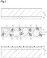
- FIG. 1 is a schematic cross-sectional view showing an embodiment of a method of manufacturing a connection structure.
- FIG. 2 is a schematic cross-sectional view showing an embodiment of a connection structure.
- FIG. 3 is a schematic view showing a method of manufacturing a connection structure for evaluation in examples.
- FIG. 4 is a schematic view showing a method of measuring connection resistance in examples.
- FIG. 1 is a schematic cross-sectional view showing an embodiment of a method of manufacturing a connection structure. As shown in FIG. 1 , first of all, a first electronic member 1 , a second electronic member 2 , and an adhesive film (adhesive layer) 3 are prepared.
- the first electronic member 1 includes a first substrate 4 , a first electrode 5 formed on a main surface of the first substrate 4 , and an insulating layer 6 formed on a side of the first electrode 5 opposite to the first substrate 4 .
- the second electronic member 2 includes a second substrate 7 and a second electrode 8 formed on a main surface of the second substrate 7 .
- the second electronic member may further include an insulating layer similar to that of the first electronic member 1 on the side of the second electrode 8 opposite to the second substrate 7 .
- the first electronic member and the second electronic member may be the same as or different from each other.
- Each of the first substrate 4 and the second substrate 7 may be a substrate formed of glass, ceramic, polyimide, polycarbonate, polyester, polyethersulfone, or the like.
- Each of the first electrode 5 and the second electrode 8 may be an electrode formed of gold, silver, copper, tin, aluminum, ruthenium, rhodium, palladium, osmium, iridium, platinum, indium tin oxide (ITO), or the like.
- the thickness of each of the first electrode 5 and the second electrode 8 may be, for example, 5 ⁇ m or more, 10 ⁇ m or more, or 20 ⁇ m or more, and may be 200 ⁇ m or less, 100 ⁇ m or less, or 50 ⁇ m or less.
- the insulating layer 6 is formed of, for example, a polymer such as polyolefin such as polypropylene or polyamide such as nylon.
- the thickness of the insulating layer 6 may be, for example, 1 ⁇ m or more, 2 ⁇ m or more, or 3 ⁇ m or more, and may be 8 ⁇ m or less, 6 ⁇ m or less, or 4 ⁇ m or less.
- the insulating layer 6 is formed by, for example, disposing an insulating film such as a film of the above-described polymer on the first electrode 5 which is formed on the main surface of the first substrate 4 .
- the adhesive film 3 is formed of an adhesive layer containing an adhesive component 9 and a first conductive particle 10 and a second conductive particle 11 which are dispersed in the adhesive component 9 .
- the adhesive component 9 is composed of, for example, a material exhibiting curability by heat or light, and may be an epoxy type adhesive, a radically curable adhesive, and a thermoplastic adhesive containing polyurethane, polyvinyl ester or the like. Since the adhesive component 9 is excellent in heat resistance and moisture resistance after adhesion, the adhesive component may be composed of a crosslinkable material.
- the epoxy type adhesive contains an epoxy resin which is a thermosetting resin as a main component.
- the epoxy type adhesive is preferably used from the viewpoint that the epoxy type adhesive can be cured in a short time, has good connection workability, is excellent in adhesiveness, and the like.
- the radically curable adhesive has properties such as being excellent in curability at a low temperature in a short time as compared with the epoxy type adhesive, and is therefore suitably used according to the application.
- the epoxy type adhesive contains, for example, an epoxy resin (thermosetting material) and a curing agent, and may further contain a thermoplastic resin, a coupling agent, a filler, and the like as necessary.
- the epoxy resin examples include a bisphenol A type epoxy resin, a bisphenol F type epoxy resin, a bisphenol S type epoxy resin, a phenol novolak type epoxy resin, a cresol novolak type epoxy resin, a bisphenol A novolak type epoxy resin, a bisphenol F novolak type epoxy resin, an alicyclic epoxy resin, a glycidyl ester type epoxy resin, a glycidyl amine type epoxy resin, a hydantoin type epoxy resin, an isocyanurate type epoxy resin, and an aliphatic chain epoxy resin.
- These epoxy resins may be halogenated or hydrogenated, and may have a structure in which an acryloyl group or a methacryloyl group is added to a side chain. These epoxy resins are used singly or in combinations of two or more.
- the curing agent is not particularly limited as long as the curing agent can cure the epoxy resin, and examples thereof include an anionic polymerization catalyst type curing agent, a cationic polymerization catalyst type curing agent, and a polyaddition type curing agent.
- the curing agent is preferable to be an anionic or cationic polymerization catalyst type curing agent from the viewpoint of excellent fast curability and no need for chemical equivalent consideration.
- anionic or cationic polymerization catalyst type curing agent may include an imidazole, a hydrazide, a boron trifluoride-amine complex, an onium salt (aromatic sulfonium salt, aromatic diazonium salt, aliphatic sulfonium salt, and the like), an amine imide, a diaminomaleonitrile, a melamine and its derivatives, a polyamine salt, a dicyandiamide, and these modified products.
- the polyaddition type curing agent include a polyamine, a polymercaptan, a polyphenol, and an acid anhydride.
- These curing agents may be latent curing agents that are microencapsulated by being coated with polymer substances such as polyurethanes and polyesters, metal thin films of nickel, copper, and the like, inorganic substances such as calcium silicate.
- the latent curing agent is preferable since the pot life can be extended.
- the curing agents are used singly or in combinations of two or more.
- the content of the curing agent may be 0.05 to 20 parts by mass with respect to 100 parts by mass of the total amount of the thermosetting material and the thermoplastic resin added as necessary.
- a radically curable adhesive contains, for example, a radical polymerizable material and a radical polymerization initiator (also referred to as a curing agent), and may further contain a thermoplastic resin, a coupling agent, a filler, and the like, as necessary.
- radical polymerizable material for example, any material having a functional group which is polymerized by radical can be used without particular limitation.
- radical polymerizable materials may include an acrylate (including corresponding methacrylate, the same applies hereinafter) compound, an acryloxy (including corresponding methacryloxy, the same applies hereinafter) compound, a maleimide compound, a citraconimide resin, and a nadimide resin.
- These radical polymerizable materials may be in a state of a monomer or a state of an oligomer, or may be in a mixture state of a monomer and an oligomer.
- Examples of an acrylate compound include methyl acrylate, ethyl acrylate, isopropyl acrylate, isobutyl acrylate, ethylene glycol diacrylate, diethylene glycol diacrylate, trimethylolpropane triacrylate, tetramethylolmethane tetraacrylate, 2-hydroxy-1,3-diacryloxypropane, 2,2-bis[4-(acryloxymethoxy)phenyl]propane, 2,2-bis[4-(acryloxypolyethoxy)phenyl]propane, dicyclopentenyl acrylate, tricyclodecanyl acrylate, tris(acryloyloxyethyl)isocyanurate, urethane acrylate, and phosphoric acid ester diacrylate.
- a radical polymerizable material such as an acrylate compound may be used together with a polymerization inhibitor such as hydroquinone and methyl ether hydroquinone as necessary.
- the radical polymerizable material such as an acrylate compound preferably has at least one substituent such as a dicyclopentenyl group, a tricyclodecanyl group, and a triazine ring.
- the radical polymerizable material other than the acrylate compound for example, the compound described in International Publication No. WO 2009/063827 can be suitably used.
- the radical polymerizable materials may be used singly or in combinations of two or more.
- radical polymerization initiator for example, any compound capable of decomposing upon heating or irradiation with light to generate radicals can be used without particular limitation.
- Specific examples of the radical polymerization initiator may include a peroxide compound an azo compound. These compounds are appropriately selected depending on the target connection temperature, connection time, pot life, and the like.
- radical polymerization initiator preferably include diacyl peroxide, peroxy dicarbonate, peroxy ester, peroxy ketal, dialkyl peroxide, hydroperoxide, and silyl peroxide.
- peroxy ester, dialkyl peroxide, hydroperoxide, and silyl peroxide and the like are preferable, and peroxy ester is more preferable from the viewpoint of being capable of obtaining high reactivity.
- the radical polymerization initiators for example, the compound described in International Publication No. WO 2009/063827 can be suitably used.
- the radical polymerization initiators are used singly or in combinations of two or more.
- the content of the radical polymerization initiator may be 0.1 to 10 parts by mass with respect to 100 parts by mass of the total amount of the radical polymerizable material and the thermoplastic resin added as necessary.
- thermoplastic resin which is blended as necessary in the epoxy type adhesive and the radically curable adhesive makes it easy to provide excellent film formability to the adhesive, for example.
- thermoplastic resin include a phenoxy resin, a polyvinyl formal resin, a polystyrene resin, a polyvinyl butyral resin, a polyester resin, a polyamide resin, a xylene resin, a polyurethane resin, a polyester urethane resin, a phenol resin, and a terpene phenol resin.
- the thermoplastic resin for example, the compound described in International Publication No. WO 2009/063827 can be suitably used.
- a phenoxy resin is preferable since adhesiveness, compatibility, heat resistance, mechanical strength, and the like are excellent.
- the thermoplastic resins are used singly or in combinations of two or more.
- the content of the thermoplastic resin may be 5 to 80 parts by mass with respect to 100 parts by mass of the total amount of the thermoplastic resin and the thermosetting material when the thermoplastic resin is added to the epoxy type adhesive.
- the content of the thermoplastic resin may be 5 to 80 parts by mass with respect to 100 parts by mass of the total amount of the thermoplastic resin and the radical polymerizable material when the thermoplastic resin is added to the radically curable adhesive.
- the adhesive component 9 includes a thermal radical curable adhesive containing a thermoplastic resin, a radical polymerizable material in a liquid state at 30° C., and a radical polymerization initiator.
- the thermal radical curable adhesive has a lower viscosity than the above adhesive component.
- the content of the radical polymerizable material in the thermal radical curable adhesive is preferably 20 to 80 parts by mass, more preferably 30 to 80 parts by mass, and further preferably 40 to 80 parts by mass, with respect to 100 parts by mass of the total amount of the thermoplastic resin and the radical polymerizable material.
- the adhesive component 9 may be an epoxy type adhesive containing a thermoplastic resin, a thermosetting material including an epoxy resin in a liquid state at 30° C., and a curing agent.
- the content of the epoxy resin in the epoxy type adhesive is preferably 20 to 80 parts by mass, more preferably 40 to 80 parts by mass, and further preferably 30 to 80 parts by mass, with respect to 100 parts by mass of the total amount of the thermoplastic resin and the thermosetting material.
- the adhesive component 9 preferably further comprises a component that exerts an effect of relaxing the internal stress, from the viewpoint of suppressing the warping of the substrate caused by the difference in linear expansion coefficient between the IC chip and the substrate.
- a component that exerts an effect of relaxing the internal stress include an acrylic rubber and an elastomer component.
- the adhesive component 9 may be a radical curable adhesive as described in International Publication No. WO 98/44067.
- the volume proportion of the adhesive component 9 in the adhesive film 3 may be 55% by volume or more or 65% by volume or more, and 95% by volume or less or 85% by volume or less, based on the total volume of the adhesive film 3 .
- the first conductive particle 10 exhibits a dendritic shape (also referred to as a dendrite shape) and comprises one main shaft and a plurality of branches that two-dimensionally or three-dimensionally branch from the main shaft.
- the first conductive particle 10 may be formed from a metal such as copper or silver, and may be, for example, a silver-coated copper particle in which a copper particle is coated with silver.
- the first conductive particle 10 may be known one, and specifically is available, for example, as ACBY-2 (Mitsui Mining & Smelting Co., Ltd.), CE-1110 (Fukuda Metal Foil & Powder Co., Ltd.), #FSP (JX Nippon Mining & Metals Corporation), and #51-R (JX Nippon Mining & Metals Corporation).
- the first conductive particle 10 can also be manufactured by a known method (for example, the method described in the above Patent Literature 1).
- the content of the first conductive particle 10 in the adhesive film 3 (the volume proportion of the first conductive particle 10 in the adhesive film 3 ) may be 2% by volume or more or 8% by volume or more, and 25% by volume or less or 15% by volume or less, based on the total volume of the adhesive film 3 .
- the second conductive particle 11 has a nonconductive core body and a conductive layer provided on the core body.
- the core body is formed from a nonconductive material such as glass, ceramic, and resin, and is preferably formed from resin.
- the resin include an acrylic resin, a styrene resin, a silicone resin, a polybutadiene resin, or copolymers of monomers constituting these resins.
- the average particle diameter of the core body may be, for example, 2 to 30 ⁇ m.
- the conductive layer is formed from, for example, gold, silver, copper, nickel, palladium, or an alloy thereof. From the viewpoint of excellent conductivity, the conductive layer preferably comprises at least one selected from gold, nickel, and palladium, more preferably comprises gold or palladium, and further preferably comprises gold.
- the conductive layer is formed, for example, by plating the above metal on the core body.
- the thickness of the conductive layer may be, for example, 10 to 400 nm.
- the average particle diameter of the second conductive particle 11 is preferably 30 ⁇ m or less, more preferably 25 ⁇ m or less, and further preferably 20 ⁇ m or less, from the viewpoint that the film can be suitably thinned.
- the average particle diameter of the second conductive particle 11 may be, for example, 1 ⁇ m or more.
- the average particle diameters of the second conductive particle 11 and the core constituting it are measured by a particle size distribution measuring apparatus (Microtrac (product name, Nikkiso Co., Ltd.)) using a laser diffraction-scattering method.
- the content of the second conductive particle 11 in the adhesive film 3 may be 2% by volume or more or 5% by volume or more, and 20% by volume or less or 10% by volume or less, based on the total volume of the adhesive film 3 .
- the thickness of the adhesive film 3 may be, for example, 5 ⁇ m or more, 7 ⁇ m or more, or 10 ⁇ m or more, and may be 30 ⁇ m or less, 25 ⁇ m or less, or 20 ⁇ m or less.
- the adhesive layer may be prepared by, for example, applying a paste-like adhesive composition onto the first electronic member 1 or the second electronic member 2 .
- the paste-like adhesive composition is obtained by, for example, heating a mixture containing the adhesive component, the first conductive particles, and the second conductive particles, or dissolving the mixture in a solvent.
- a solvent for example, a solvent having a boiling point of 50 to 150° C. under atmospheric pressure is used.
- the adhesive film (adhesive layer) 3 is disposed between the first electronic member 1 and the second electronic member 2 , and the first electronic member 1 and the second electronic member 2 are pressure-bonded to each other via the adhesive film (adhesive layer) 3 .
- the first electronic member 2 , the adhesive film (adhesive layer) 3 , and the second electronic member 1 are pressed and heated in the stacking direction such that the first electrode 5 and the second electrode 8 are electrically connected to each other.
- the heating temperature is, for example, 50 to 190° C.
- the pressure is, for example, 0.1 to 30 MPa. These heating and pressurizing are performed, for example, in the range of 0.5 seconds to 120 seconds.
- FIG. 2 is a schematic cross-sectional view showing an embodiment of the connection structure.
- the connection structure 20 includes a first electronic member 1 having a first substrate 4 , a first electrode 5 formed on the first substrate 4 , and an insulating layer 6 formed on the side of the first electrode 5 opposite to the first substrate 4 , a second electronic member 2 having a second substrate 7 and a second electrode 8 formed on the second substrate 7 , and a connecting member 21 connecting the first electrode 5 and the second electrodes 8 electrically to each other.
- the connecting member 21 includes a cured product 22 of the adhesive component 9 , the first conductive particles 10 and the second conductive particles 11 which are dispersed in the cured product 22 . That is, the connecting member 21 is formed by curing the adhesive film 3 .
- the first electronic member 1 on which the insulating layer 6 can be suitably connected. That is, since the first conductive particles 10 included in the adhesive film 3 have a dendritic shape, when the electronic members 1 and 2 are pressure-bonded to each other, as shown in FIG. 2 , the first conductive particles 10 can break through the insulating layer 6 and be electrically connected to the first electrode 5 .
- the second conductive particles 11 serve as a main conductive path for electrically connecting the first electrode 5 and the second electrode 8 to each other, a suitable connection can be achieved even at a low pressure, and reliability is excellent, as compared with, for example, a case where an adhesive film containing only the first conductive particles 10 is used.
- the adhesive film 3 is composed of the adhesive layer 1 containing the adhesive component 9 , the first conductive particles 10 , and the second conductive particles 11 , but in another embodiment, the adhesive film may be composed of two or more layers.
- the first conductive particles 10 and the second conductive particles 11 may be included in at least one layer of the two or more layers, and may be included in the same layer as or different layers from each other.
- the adhesive component 9 , the first conductive particles 10 , and second conductive particles 11 included in two or more layers may be the same as or different from each other.
- the adhesive film may include a first adhesive layer containing the first conductive particles 10 and a second adhesive layer containing the second conductive particles 11 .
- the first adhesive layer may not contain the second conductive particles 11
- the second adhesive layer may not contain the first conductive particles 10 .
- the first adhesive layer containing the first conductive particles 10 is preferably disposed toward the first electronic member 1 having the insulating layer 6 when the adhesive film is disposed between the electronic members 1 and 2 , from the viewpoint of more suitably obtaining the above-described effect that the first conductive particles 10 break through the insulating layer 6 .
- the adhesive film may include a first adhesive layer containing the first conductive particles 10 and the second conductive particles 11 and a second adhesive layer containing no conductive particles (consisting of only the adhesive component).
- the first adhesive layer containing the first conductive particles 10 is preferably disposed toward the first electronic member 1 having the insulating layer 6 when the adhesive film is disposed between the electronic members 1 and 2 , from the viewpoint of more suitably obtaining the above-described effect that the first conductive particles 10 break through the insulating layer 6 .
- this adhesive film is suitably used, for example, when the second electrode 8 of the second electronic member 2 has an uneven shape. That is, in this adhesive film, since the second adhesive layer (adhesive component) containing no conductive particles easily flows, it can flow along the uneven shape of the second electrode 8 when the electronic members 1 and 2 are pressure-bonded. Therefore, since the adhesive component is satisfactorily filled between the electronic members 1 and 2 , the electronic members 1 and 2 can be suitably bonded to each other.
- the adhesive film may include a first adhesive layer containing the first conductive particles 10 , a second adhesive layer containing the second conductive particles 11 , and a third adhesive layer containing the first conductive particles 10 in this order.
- the first adhesive layer and the third adhesive layer may not contain the second conductive particles 11
- the second adhesive layer may not contain the first conductive particles 10 .
- the adhesive film according to this embodiment is suitably used when the insulating layer 6 is also provided on the second electronic member. That is, in this adhesive film, since the first conductive particles 10 are disposed on both sides of the adhesive film, the first conductive particles 10 can suitably break through the insulating layer 6 even when the insulating layer 6 is provided in the second electronic member.
- a phenoxy resin product name: PKHC, weight average molecular weight: 45000, manufactured by Union Carbide Corporation
- PKHC weight average molecular weight: 45000, manufactured by Union Carbide Corporation
- urethane acrylate product name: UN7700, manufactured by Negami Chemical Industrial Co., Ltd.
- phosphoric acid ester dimethacrylate product name: Light Ester P-2M, manufactured by Kyoeisha Chemical Co., Ltd.
- 1,1-bis(t-hexylperoxy)-3,3,5-trimethylcyclohexane product name: Perhexa TMH, manufactured by NOF Corporation
- the dendritic conductive particles (silver-coated copper particles, manufactured by Mitsui Mining & Smelting Co., Ltd., product name: ACBY-2) were used as conductive particles B1 (the first conductive particles).
- Benzoyl peroxide as a polymerization initiator was added to a mixed solution of divinylbenzene, styrene monomer, and butyl methacrylate, and polymerization reaction was performed by heating at high speed with uniform stirring to obtain a fine particle dispersion solution.
- This fine particles dispersion solution was filtered and dried under reduced pressure to obtain a block body which was an aggregate of fine particles.
- This block body was pulverized to prepare core bodies (resin particles) having an average particle diameter of 20 ⁇ m and different crosslinking density.
- a palladium catalyst (product name: MK-2605, manufactured by Muromachi Technos Co., Ltd.) was supported on the surface of the above core bodies, and the core bodies were activated with an accelerator (product name: MK-370, manufactured by Muromachi Technos Co., Ltd.).
- the core body was added to a mixed solution of nickel sulfate aqueous solution, sodium hypophosphite aqueous solution, and sodium tartrate aqueous solution heated to 60° C. to perform a pre-electroless plating step. The mixture was stirred for 20 minutes, and it was confirmed that hydrogen bubbling stopped.
- a mixed solution of nickel sulfate, sodium hypophosphite, sodium citrate, and a plating stabilizer was added and stirred until pH was stabilized, and the post-electroless plating step was performed until hydrogen bubbling stopped. Subsequently, the plating solution was filtered, the filtrate was washed with water, and then dried with a vacuum dryer at 80° C. to prepare a nickel-plated conductive particles C1 (the second conductive particles).
- the properties of the obtained adhesive film when used as a connecting member were evaluated by the following procedure.
- an adhesive film 31 obtained by cutting the obtained adhesive film into 6 mm ⁇ 6 mm was disposed substantially at the center of a 6 mm ⁇ 50 mm copper foil 32 and bonded by heating and pressing (50° C., 0.1 MPa, 2 seconds) using BD-07 manufactured by Ohashi Seisakusho Co., Ltd. Subsequently, as shown in FIGS.
- the aluminum laminate film 33 was placed on the laminate of the copper foil 32 and the adhesive film 31 to cover the adhesive film 31 , and the laminate was heated and pressed (150° C., 1.0 MPa, 10 seconds) by BD-07 manufactured by Ohashi Seisakusho Co., Ltd.
- connection structure for evaluation in which the copper foil 32 , the adhesive film 31 , the insulating layer (polypropylene layer), and the aluminum foil were laminated in this order was obtained.
- An ammeter and a voltmeter were connected to the obtained connection structure as shown in FIG. 4 , and the connection resistance (initial) was measured by a four-terminal method. The results are shown in Table 1.
- an adhesive film 31 obtained by cutting the obtained adhesive film into 6 mm ⁇ 6 mm was disposed substantially at the center of a 6 mm ⁇ 50 mm copper foil 32 and bonded by heating and pressing (50° C., 0.5 MPa, 2 seconds) using BD-07 manufactured by Ohashi Seisakusho Co., Ltd. Subsequently, as shown in FIGS.
- An aluminum laminate film 33 was placed on the laminate of the copper foil 32 and the adhesive film 31 to cover the adhesive film 31 , and the laminate was heated and pressed (150° C., 3.0 MPa, 10 seconds) by BD-07 manufactured by Ohashi Seisakusho Co., Ltd.
- BD-07 manufactured by Ohashi Seisakusho Co., Ltd.
- connection resistance (initial) was measured by a four-terminal method.
- the resistance was measured after the terminal was strongly pressed and sufficiently conducted.
- a heat cycle test in which a heat cycle of holding at ⁇ 20° C. for 30 minutes, increasing the temperature to 100° C. over 10 minutes, holding at 100° C. for 30 minutes, and decreasing the temperature to ⁇ 20° C. over 10 minutes was repeated 500 times was performed on the connection structure using TSA-43EL manufactured by ESPEC CORP., and then the connection resistance (after the heat cycle test) was measured in the same manner as described above. The results are shown in Table 1.
- a preparation of an adhesive film, and a preparation and evaluation of a connection structure were performed in the same manner as in Example 1 except that the conductive particles B1 (first conductive particles) were not used in the adhesive layer.
- a preparation of an adhesive film, and a preparation and evaluation of a connection structure were performed in the same manner as in Example 1 except that the conductive particles C1 (second conductive particles) were not used in the adhesive layer.
- first electronic member 1 : first electronic member
- 2 second electronic member
- 3 adhesive film (adhesive layer)
- 4 first substrate
- 5 first electrode
- 6 insulating layer
- 7 second substrate
- 8 second electrode
- 10 first conductive particle
- 11 second conductive particle
- 20 connection structure
- 21 connecting member.
Landscapes
- Engineering & Computer Science (AREA)
- Chemical & Material Sciences (AREA)
- Organic Chemistry (AREA)
- Manufacturing & Machinery (AREA)
- Microelectronics & Electronic Packaging (AREA)
- Inorganic Chemistry (AREA)
- Adhesives Or Adhesive Processes (AREA)
- Conductive Materials (AREA)
- Manufacturing Of Electrical Connectors (AREA)
- Glass Compositions (AREA)
Abstract
Description
| TABLE 1 | ||||
| Comparative | Comparative | |||
| Example 1 | Example 1 | Example 2 | ||
| Conductivity in | 0.48 | 2.6 | 3.9 |
| Low-Pressure Connection | |||
| (connection resistance/Ω) |
| Reliability | Initial | 0.22 | 1.56 | 0.76 |
| (connection | After | 0.35 | 22.5 | 8.7 |
| resistance/Ω) | heat cycle test | |||
Claims (12)
Applications Claiming Priority (4)
| Application Number | Priority Date | Filing Date | Title |
|---|---|---|---|
| JP2017-254726 | 2017-12-28 | ||
| JPJP2017-254726 | 2017-12-28 | ||
| JP2017254726 | 2017-12-28 | ||
| PCT/JP2018/048242 WO2019131904A1 (en) | 2017-12-28 | 2018-12-27 | Connection structure and method for producing same |
Publications (2)
| Publication Number | Publication Date |
|---|---|
| US20200321305A1 US20200321305A1 (en) | 2020-10-08 |
| US11355469B2 true US11355469B2 (en) | 2022-06-07 |
Family
ID=67063791
Family Applications (1)
| Application Number | Title | Priority Date | Filing Date |
|---|---|---|---|
| US16/957,568 Active US11355469B2 (en) | 2017-12-28 | 2018-12-27 | Connection structure and method for producing same |
Country Status (6)
| Country | Link |
|---|---|
| US (1) | US11355469B2 (en) |
| JP (1) | JP7314801B2 (en) |
| KR (1) | KR102732406B1 (en) |
| CN (1) | CN111512502B (en) |
| TW (1) | TWI797225B (en) |
| WO (1) | WO2019131904A1 (en) |
Families Citing this family (5)
| Publication number | Priority date | Publication date | Assignee | Title |
|---|---|---|---|---|
| WO2018042701A1 (en) | 2016-08-30 | 2018-03-08 | 日立化成株式会社 | Adhesive composition |
| WO2021177375A1 (en) * | 2020-03-04 | 2021-09-10 | 昭和電工マテリアルズ株式会社 | Adhesive film and reel body |
| KR102470033B1 (en) * | 2020-12-21 | 2022-11-23 | 한국전자기술연구원 | Device mounting sinterable bonding material comprising dendritic metal powder and semiconductor device package using the same |
| TWI884347B (en) * | 2021-03-26 | 2025-05-21 | 日商拓自達電線股份有限公司 | Conductive adhesive layer |
| JPWO2024190620A1 (en) * | 2023-03-13 | 2024-09-19 |
Citations (21)
| Publication number | Priority date | Publication date | Assignee | Title |
|---|---|---|---|---|
| JPH10116640A (en) | 1997-05-23 | 1998-05-06 | Hitachi Chem Co Ltd | Connection structure for circuit |
| WO2001064807A1 (en) | 2000-02-29 | 2001-09-07 | Matsushita Electric Industrial Co., Ltd. | Conductive adhesive, apparatus for mounting electronic component, and method for mounting the same |
| US20010028953A1 (en) | 1998-11-16 | 2001-10-11 | 3M Innovative Properties Company | Adhesive compositions and methods of use |
| JP2003045229A (en) | 2001-07-27 | 2003-02-14 | Toppan Forms Co Ltd | Conductive adhesive and method of mounting IC chip using the same |
| US6787233B1 (en) | 1998-10-19 | 2004-09-07 | Dynal Biotech Asa | Particles |
| JP2006108523A (en) | 2004-10-08 | 2006-04-20 | Hitachi Chem Co Ltd | Method of connecting electrical component using anisotropic conductive film |
| US20080230749A1 (en) | 2004-05-19 | 2008-09-25 | Bridgestone Corporation | Adhesive Agent Composition and Adhesive Film For Electronic Component |
| US20090133900A1 (en) * | 2005-04-14 | 2009-05-28 | Matsushita Electric Industrial Co., Ltd. | Electronic circuit device and method for manufacturing same |
| US20090189254A1 (en) * | 2005-08-22 | 2009-07-30 | Hitachi Chemical Dupont Microsystems, Ltd. | Circuit connection structure, method for producing the same and semiconductor substrate for circuit connection structure |
| JP2012028334A (en) | 2011-09-07 | 2012-02-09 | Sony Chemical & Information Device Corp | Anisotropic conductive film and method of manufacturing connecting structure |
| US20120177930A1 (en) | 2009-07-08 | 2012-07-12 | Anja Henckens | Electrically Conductive Adhesives |
| WO2013035164A1 (en) | 2011-09-06 | 2013-03-14 | 日立化成株式会社 | Adhesive composition and connection body |
| WO2013150907A1 (en) | 2012-04-02 | 2013-10-10 | 株式会社スリーボンド | Electroconductive composition |
| CN103548207A (en) | 2011-05-18 | 2014-01-29 | 日立化成株式会社 | Circuit connection material, connection structure of circuit components, and manufacturing method of connection structure of circuit components |
| WO2014021037A1 (en) | 2012-08-02 | 2014-02-06 | 三井金属鉱業株式会社 | Electroconductive film |
| JP2014078478A (en) | 2012-09-24 | 2014-05-01 | Tamura Seisakusho Co Ltd | Anisotropic conductive paste and printed wiring board using the same |
| US20150129812A1 (en) | 2012-05-04 | 2015-05-14 | Tesa Se | Three-dimensional electrically conductive adhesive film |
| JP2015097240A (en) | 2013-11-15 | 2015-05-21 | 三井金属鉱業株式会社 | Metal foil for press bonding and electronic component package |
| TW201739327A (en) | 2016-03-25 | 2017-11-01 | 迪睿合股份有限公司 | Method for manufacturing connection structure |
| US20190241770A1 (en) | 2016-08-30 | 2019-08-08 | Hitachi Chemical Company, Ltd. | Adhesive composition |
| US10633559B2 (en) * | 2009-12-21 | 2020-04-28 | Tesa Se | Heat-activated, glueable surface elements |
Family Cites Families (3)
| Publication number | Priority date | Publication date | Assignee | Title |
|---|---|---|---|---|
| WO2005002002A1 (en) * | 2003-06-25 | 2005-01-06 | Hitachi Chemical Co., Ltd. | Circuit connecting material, film-like circuit connecting material using the same, circuit member connecting structure, and method of producing the same |
| JP4019328B2 (en) * | 2006-06-08 | 2007-12-12 | 日立化成工業株式会社 | Electrode connection method |
| JP5916334B2 (en) * | 2011-10-07 | 2016-05-11 | デクセリアルズ株式会社 | Anisotropic conductive adhesive and manufacturing method thereof, light emitting device and manufacturing method thereof |
-
2018
- 2018-12-27 JP JP2019562183A patent/JP7314801B2/en active Active
- 2018-12-27 KR KR1020207020835A patent/KR102732406B1/en active Active
- 2018-12-27 WO PCT/JP2018/048242 patent/WO2019131904A1/en not_active Ceased
- 2018-12-27 CN CN201880082955.2A patent/CN111512502B/en active Active
- 2018-12-27 US US16/957,568 patent/US11355469B2/en active Active
- 2018-12-28 TW TW107147600A patent/TWI797225B/en active
Patent Citations (23)
| Publication number | Priority date | Publication date | Assignee | Title |
|---|---|---|---|---|
| JPH10116640A (en) | 1997-05-23 | 1998-05-06 | Hitachi Chem Co Ltd | Connection structure for circuit |
| US6787233B1 (en) | 1998-10-19 | 2004-09-07 | Dynal Biotech Asa | Particles |
| US20010028953A1 (en) | 1998-11-16 | 2001-10-11 | 3M Innovative Properties Company | Adhesive compositions and methods of use |
| WO2001064807A1 (en) | 2000-02-29 | 2001-09-07 | Matsushita Electric Industrial Co., Ltd. | Conductive adhesive, apparatus for mounting electronic component, and method for mounting the same |
| JP2003045229A (en) | 2001-07-27 | 2003-02-14 | Toppan Forms Co Ltd | Conductive adhesive and method of mounting IC chip using the same |
| US20080230749A1 (en) | 2004-05-19 | 2008-09-25 | Bridgestone Corporation | Adhesive Agent Composition and Adhesive Film For Electronic Component |
| JP2006108523A (en) | 2004-10-08 | 2006-04-20 | Hitachi Chem Co Ltd | Method of connecting electrical component using anisotropic conductive film |
| US20090133900A1 (en) * | 2005-04-14 | 2009-05-28 | Matsushita Electric Industrial Co., Ltd. | Electronic circuit device and method for manufacturing same |
| US20090189254A1 (en) * | 2005-08-22 | 2009-07-30 | Hitachi Chemical Dupont Microsystems, Ltd. | Circuit connection structure, method for producing the same and semiconductor substrate for circuit connection structure |
| US20120177930A1 (en) | 2009-07-08 | 2012-07-12 | Anja Henckens | Electrically Conductive Adhesives |
| US10633559B2 (en) * | 2009-12-21 | 2020-04-28 | Tesa Se | Heat-activated, glueable surface elements |
| CN103548207A (en) | 2011-05-18 | 2014-01-29 | 日立化成株式会社 | Circuit connection material, connection structure of circuit components, and manufacturing method of connection structure of circuit components |
| CN103764776A (en) | 2011-09-06 | 2014-04-30 | 日立化成株式会社 | Adhesive compositions and linkers |
| WO2013035164A1 (en) | 2011-09-06 | 2013-03-14 | 日立化成株式会社 | Adhesive composition and connection body |
| JP2012028334A (en) | 2011-09-07 | 2012-02-09 | Sony Chemical & Information Device Corp | Anisotropic conductive film and method of manufacturing connecting structure |
| TW201348400A (en) | 2012-04-02 | 2013-12-01 | Three Bond Co Ltd | Electroconductive composition |
| WO2013150907A1 (en) | 2012-04-02 | 2013-10-10 | 株式会社スリーボンド | Electroconductive composition |
| US20150129812A1 (en) | 2012-05-04 | 2015-05-14 | Tesa Se | Three-dimensional electrically conductive adhesive film |
| WO2014021037A1 (en) | 2012-08-02 | 2014-02-06 | 三井金属鉱業株式会社 | Electroconductive film |
| JP2014078478A (en) | 2012-09-24 | 2014-05-01 | Tamura Seisakusho Co Ltd | Anisotropic conductive paste and printed wiring board using the same |
| JP2015097240A (en) | 2013-11-15 | 2015-05-21 | 三井金属鉱業株式会社 | Metal foil for press bonding and electronic component package |
| TW201739327A (en) | 2016-03-25 | 2017-11-01 | 迪睿合股份有限公司 | Method for manufacturing connection structure |
| US20190241770A1 (en) | 2016-08-30 | 2019-08-08 | Hitachi Chemical Company, Ltd. | Adhesive composition |
Also Published As
| Publication number | Publication date |
|---|---|
| JP7314801B2 (en) | 2023-07-26 |
| US20200321305A1 (en) | 2020-10-08 |
| TW201933964A (en) | 2019-08-16 |
| KR102732406B1 (en) | 2024-11-19 |
| WO2019131904A1 (en) | 2019-07-04 |
| JPWO2019131904A1 (en) | 2020-12-24 |
| TWI797225B (en) | 2023-04-01 |
| CN111512502A (en) | 2020-08-07 |
| CN111512502B (en) | 2022-06-03 |
| KR20200103043A (en) | 2020-09-01 |
Similar Documents
| Publication | Publication Date | Title |
|---|---|---|
| US12163073B2 (en) | Connected electronic members | |
| US11355469B2 (en) | Connection structure and method for producing same | |
| JP7347576B2 (en) | adhesive film | |
| JP2023029350A (en) | adhesive film | |
| US12134720B2 (en) | Adhesive film | |
| US12227683B2 (en) | Connector production method and adhesive film |
Legal Events
| Date | Code | Title | Description |
|---|---|---|---|
| FEPP | Fee payment procedure |
Free format text: ENTITY STATUS SET TO UNDISCOUNTED (ORIGINAL EVENT CODE: BIG.); ENTITY STATUS OF PATENT OWNER: LARGE ENTITY |
|
| AS | Assignment |
Owner name: HITACHI CHEMICAL COMPANY, LTD., JAPAN Free format text: ASSIGNMENT OF ASSIGNORS INTEREST;ASSIGNORS:SHIRAKAWA, TETSUYUKI;FUKUI, TAKAHIRO;IWAMOTO, SHINNOSUKE;SIGNING DATES FROM 20200701 TO 20200704;REEL/FRAME:053626/0974 |
|
| STPP | Information on status: patent application and granting procedure in general |
Free format text: DOCKETED NEW CASE - READY FOR EXAMINATION |
|
| STPP | Information on status: patent application and granting procedure in general |
Free format text: NON FINAL ACTION MAILED |
|
| STPP | Information on status: patent application and granting procedure in general |
Free format text: RESPONSE TO NON-FINAL OFFICE ACTION ENTERED AND FORWARDED TO EXAMINER |
|
| STPP | Information on status: patent application and granting procedure in general |
Free format text: NOTICE OF ALLOWANCE MAILED -- APPLICATION RECEIVED IN OFFICE OF PUBLICATIONS |
|
| AS | Assignment |
Owner name: SHOWA DENKO MATERIALS CO., LTD., JAPAN Free format text: CHANGE OF NAME;ASSIGNOR:HITACHI CHEMICAL COMPANY, LTD.;REEL/FRAME:059858/0916 Effective date: 20201001 |
|
| STPP | Information on status: patent application and granting procedure in general |
Free format text: AWAITING TC RESP, ISSUE FEE PAYMENT RECEIVED |
|
| STPP | Information on status: patent application and granting procedure in general |
Free format text: AWAITING TC RESP, ISSUE FEE PAYMENT VERIFIED |
|
| STCF | Information on status: patent grant |
Free format text: PATENTED CASE |
|
| AS | Assignment |
Owner name: RESONAC CORPORATION, JAPAN Free format text: CHANGE OF NAME;ASSIGNOR:SHOWA DENKO MATERIALS CO., LTD.;REEL/FRAME:062992/0805 Effective date: 20230101 |
|
| AS | Assignment |
Owner name: RESONAC CORPORATION, JAPAN Free format text: CHANGE OF ADDRESS;ASSIGNOR:RESONAC CORPORATION;REEL/FRAME:066599/0037 Effective date: 20231001 |
|
| MAFP | Maintenance fee payment |
Free format text: PAYMENT OF MAINTENANCE FEE, 4TH YEAR, LARGE ENTITY (ORIGINAL EVENT CODE: M1551); ENTITY STATUS OF PATENT OWNER: LARGE ENTITY Year of fee payment: 4 |