JP5916334B2 - Anisotropic conductive adhesive and manufacturing method thereof, light emitting device and manufacturing method thereof - Google Patents
Anisotropic conductive adhesive and manufacturing method thereof, light emitting device and manufacturing method thereof Download PDFInfo
- Publication number
- JP5916334B2 JP5916334B2 JP2011222498A JP2011222498A JP5916334B2 JP 5916334 B2 JP5916334 B2 JP 5916334B2 JP 2011222498 A JP2011222498 A JP 2011222498A JP 2011222498 A JP2011222498 A JP 2011222498A JP 5916334 B2 JP5916334 B2 JP 5916334B2
- Authority
- JP
- Japan
- Prior art keywords
- light
- anisotropic conductive
- conductive adhesive
- light emitting
- emitting element
- Prior art date
- Legal status (The legal status is an assumption and is not a legal conclusion. Google has not performed a legal analysis and makes no representation as to the accuracy of the status listed.)
- Active
Links
- 239000000853 adhesive Substances 0.000 title claims description 78
- 230000001070 adhesive effect Effects 0.000 title claims description 78
- 238000004519 manufacturing process Methods 0.000 title claims description 21
- 239000002245 particle Substances 0.000 claims description 88
- 239000002184 metal Substances 0.000 claims description 69
- 229910052751 metal Inorganic materials 0.000 claims description 69
- 239000010410 layer Substances 0.000 claims description 57
- 239000011247 coating layer Substances 0.000 claims description 39
- 238000000034 method Methods 0.000 claims description 37
- BQCADISMDOOEFD-UHFFFAOYSA-N Silver Chemical compound [Ag] BQCADISMDOOEFD-UHFFFAOYSA-N 0.000 claims description 29
- 229910052709 silver Inorganic materials 0.000 claims description 29
- 239000004332 silver Substances 0.000 claims description 29
- 229920005989 resin Polymers 0.000 claims description 25
- 239000011347 resin Substances 0.000 claims description 25
- 229910001316 Ag alloy Inorganic materials 0.000 claims description 16
- 238000004544 sputter deposition Methods 0.000 claims description 16
- 239000004840 adhesive resin Substances 0.000 claims description 13
- 229920006223 adhesive resin Polymers 0.000 claims description 13
- 229910052737 gold Inorganic materials 0.000 claims description 13
- 239000003795 chemical substances by application Substances 0.000 claims description 11
- 238000007747 plating Methods 0.000 claims description 9
- 229910052802 copper Inorganic materials 0.000 claims description 6
- 229910052782 aluminium Inorganic materials 0.000 claims description 5
- 229910052804 chromium Inorganic materials 0.000 claims description 5
- 229910052733 gallium Inorganic materials 0.000 claims description 5
- 229910052732 germanium Inorganic materials 0.000 claims description 5
- 229910052735 hafnium Inorganic materials 0.000 claims description 5
- 229910052738 indium Inorganic materials 0.000 claims description 5
- 229910052741 iridium Inorganic materials 0.000 claims description 5
- 229910052742 iron Inorganic materials 0.000 claims description 5
- 229910052750 molybdenum Inorganic materials 0.000 claims description 5
- 229910052763 palladium Inorganic materials 0.000 claims description 5
- 229910052697 platinum Inorganic materials 0.000 claims description 5
- 229910052703 rhodium Inorganic materials 0.000 claims description 5
- 229910052707 ruthenium Inorganic materials 0.000 claims description 5
- 229910052710 silicon Inorganic materials 0.000 claims description 5
- 229910052715 tantalum Inorganic materials 0.000 claims description 5
- 229910052718 tin Inorganic materials 0.000 claims description 5
- 229910052721 tungsten Inorganic materials 0.000 claims description 5
- 229910052720 vanadium Inorganic materials 0.000 claims description 5
- 229910052725 zinc Inorganic materials 0.000 claims description 5
- 229910052726 zirconium Inorganic materials 0.000 claims description 5
- 229910052779 Neodymium Inorganic materials 0.000 claims description 4
- 229910052797 bismuth Inorganic materials 0.000 claims description 4
- 150000002739 metals Chemical class 0.000 claims description 4
- 229910052719 titanium Inorganic materials 0.000 claims description 4
- 229910045601 alloy Inorganic materials 0.000 claims description 3
- 239000000956 alloy Substances 0.000 claims description 3
- 239000003292 glue Substances 0.000 claims description 2
- PXHVJJICTQNCMI-UHFFFAOYSA-N Nickel Chemical compound [Ni] PXHVJJICTQNCMI-UHFFFAOYSA-N 0.000 description 26
- 238000013508 migration Methods 0.000 description 21
- 230000005012 migration Effects 0.000 description 21
- 230000000052 comparative effect Effects 0.000 description 19
- 239000010931 gold Substances 0.000 description 14
- 239000000758 substrate Substances 0.000 description 14
- 229910052759 nickel Inorganic materials 0.000 description 13
- 239000004593 Epoxy Substances 0.000 description 12
- 150000001875 compounds Chemical class 0.000 description 12
- -1 Bi Ti Inorganic materials 0.000 description 10
- 238000012360 testing method Methods 0.000 description 9
- 210000001787 dendrite Anatomy 0.000 description 8
- PCHJSUWPFVWCPO-UHFFFAOYSA-N gold Chemical compound [Au] PCHJSUWPFVWCPO-UHFFFAOYSA-N 0.000 description 8
- LYCAIKOWRPUZTN-UHFFFAOYSA-N Ethylene glycol Chemical compound OCCO LYCAIKOWRPUZTN-UHFFFAOYSA-N 0.000 description 7
- 239000010949 copper Substances 0.000 description 7
- 239000003822 epoxy resin Substances 0.000 description 6
- 239000010419 fine particle Substances 0.000 description 6
- 229920000647 polyepoxide Polymers 0.000 description 6
- 239000010408 film Substances 0.000 description 5
- 125000003055 glycidyl group Chemical group C(C1CO1)* 0.000 description 5
- 239000000463 material Substances 0.000 description 5
- 125000002723 alicyclic group Chemical group 0.000 description 4
- 238000007772 electroless plating Methods 0.000 description 4
- 230000002349 favourable effect Effects 0.000 description 4
- 230000031700 light absorption Effects 0.000 description 4
- 239000000203 mixture Substances 0.000 description 4
- 238000007789 sealing Methods 0.000 description 4
- 239000010409 thin film Substances 0.000 description 4
- BRLQWZUYTZBJKN-UHFFFAOYSA-N Epichlorohydrin Chemical compound ClCC1CO1 BRLQWZUYTZBJKN-UHFFFAOYSA-N 0.000 description 3
- DNIAPMSPPWPWGF-UHFFFAOYSA-N Propylene glycol Chemical compound CC(O)CO DNIAPMSPPWPWGF-UHFFFAOYSA-N 0.000 description 3
- YXFVVABEGXRONW-UHFFFAOYSA-N Toluene Chemical compound CC1=CC=CC=C1 YXFVVABEGXRONW-UHFFFAOYSA-N 0.000 description 3
- 239000002253 acid Substances 0.000 description 3
- IISBACLAFKSPIT-UHFFFAOYSA-N bisphenol A Chemical compound C=1C=C(O)C=CC=1C(C)(C)C1=CC=C(O)C=C1 IISBACLAFKSPIT-UHFFFAOYSA-N 0.000 description 3
- 230000007797 corrosion Effects 0.000 description 3
- 238000005260 corrosion Methods 0.000 description 3
- LNEPOXFFQSENCJ-UHFFFAOYSA-N haloperidol Chemical class C1CC(O)(C=2C=CC(Cl)=CC=2)CCN1CCCC(=O)C1=CC=C(F)C=C1 LNEPOXFFQSENCJ-UHFFFAOYSA-N 0.000 description 3
- 125000000623 heterocyclic group Chemical group 0.000 description 3
- 238000001579 optical reflectometry Methods 0.000 description 3
- BASFCYQUMIYNBI-UHFFFAOYSA-N platinum Substances [Pt] BASFCYQUMIYNBI-UHFFFAOYSA-N 0.000 description 3
- 239000000047 product Substances 0.000 description 3
- 238000002310 reflectometry Methods 0.000 description 3
- 239000002904 solvent Substances 0.000 description 3
- 229910002070 thin film alloy Inorganic materials 0.000 description 3
- 239000011701 zinc Substances 0.000 description 3
- SVTBMSDMJJWYQN-UHFFFAOYSA-N 2-methylpentane-2,4-diol Chemical compound CC(O)CC(C)(C)O SVTBMSDMJJWYQN-UHFFFAOYSA-N 0.000 description 2
- QTWJRLJHJPIABL-UHFFFAOYSA-N 2-methylphenol;3-methylphenol;4-methylphenol Chemical compound CC1=CC=C(O)C=C1.CC1=CC=CC(O)=C1.CC1=CC=CC=C1O QTWJRLJHJPIABL-UHFFFAOYSA-N 0.000 description 2
- PAYRUJLWNCNPSJ-UHFFFAOYSA-N Aniline Chemical compound NC1=CC=CC=C1 PAYRUJLWNCNPSJ-UHFFFAOYSA-N 0.000 description 2
- 229910000881 Cu alloy Inorganic materials 0.000 description 2
- RTZKZFJDLAIYFH-UHFFFAOYSA-N Diethyl ether Chemical compound CCOCC RTZKZFJDLAIYFH-UHFFFAOYSA-N 0.000 description 2
- PEDCQBHIVMGVHV-UHFFFAOYSA-N Glycerine Chemical compound OCC(O)CO PEDCQBHIVMGVHV-UHFFFAOYSA-N 0.000 description 2
- QIGBRXMKCJKVMJ-UHFFFAOYSA-N Hydroquinone Chemical compound OC1=CC=C(O)C=C1 QIGBRXMKCJKVMJ-UHFFFAOYSA-N 0.000 description 2
- KKEYFWRCBNTPAC-UHFFFAOYSA-N Terephthalic acid Chemical compound OC(=O)C1=CC=C(C(O)=O)C=C1 KKEYFWRCBNTPAC-UHFFFAOYSA-N 0.000 description 2
- 150000008065 acid anhydrides Chemical class 0.000 description 2
- 239000002313 adhesive film Substances 0.000 description 2
- 239000011230 binding agent Substances 0.000 description 2
- 230000015572 biosynthetic process Effects 0.000 description 2
- PXKLMJQFEQBVLD-UHFFFAOYSA-N bisphenol F Chemical compound C1=CC(O)=CC=C1CC1=CC=C(O)C=C1 PXKLMJQFEQBVLD-UHFFFAOYSA-N 0.000 description 2
- YCIMNLLNPGFGHC-UHFFFAOYSA-N catechol Chemical compound OC1=CC=CC=C1O YCIMNLLNPGFGHC-UHFFFAOYSA-N 0.000 description 2
- 239000000919 ceramic Substances 0.000 description 2
- 229930003836 cresol Natural products 0.000 description 2
- 238000001035 drying Methods 0.000 description 2
- 230000000694 effects Effects 0.000 description 2
- WGCNASOHLSPBMP-UHFFFAOYSA-N hydroxyacetaldehyde Natural products OCC=O WGCNASOHLSPBMP-UHFFFAOYSA-N 0.000 description 2
- QQVIHTHCMHWDBS-UHFFFAOYSA-N isophthalic acid Chemical compound OC(=O)C1=CC=CC(C(O)=O)=C1 QQVIHTHCMHWDBS-UHFFFAOYSA-N 0.000 description 2
- 238000005259 measurement Methods 0.000 description 2
- VYKXQOYUCMREIS-UHFFFAOYSA-N methylhexahydrophthalic anhydride Chemical compound C1CCCC2C(=O)OC(=O)C21C VYKXQOYUCMREIS-UHFFFAOYSA-N 0.000 description 2
- 229920003986 novolac Polymers 0.000 description 2
- 230000003287 optical effect Effects 0.000 description 2
- KDLHZDBZIXYQEI-UHFFFAOYSA-N palladium Substances [Pd] KDLHZDBZIXYQEI-UHFFFAOYSA-N 0.000 description 2
- XNGIFLGASWRNHJ-UHFFFAOYSA-N phthalic acid Chemical compound OC(=O)C1=CC=CC=C1C(O)=O XNGIFLGASWRNHJ-UHFFFAOYSA-N 0.000 description 2
- 239000000243 solution Substances 0.000 description 2
- 238000005477 sputtering target Methods 0.000 description 2
- 239000000126 substance Substances 0.000 description 2
- 239000013077 target material Substances 0.000 description 2
- ARCGXLSVLAOJQL-UHFFFAOYSA-N trimellitic acid Chemical compound OC(=O)C1=CC=C(C(O)=O)C(C(O)=O)=C1 ARCGXLSVLAOJQL-UHFFFAOYSA-N 0.000 description 2
- NIDNOXCRFUCAKQ-UMRXKNAASA-N (1s,2r,3s,4r)-bicyclo[2.2.1]hept-5-ene-2,3-dicarboxylic acid Chemical compound C1[C@H]2C=C[C@@H]1[C@H](C(=O)O)[C@@H]2C(O)=O NIDNOXCRFUCAKQ-UMRXKNAASA-N 0.000 description 1
- JYEUMXHLPRZUAT-UHFFFAOYSA-N 1,2,3-triazine Chemical group C1=CN=NN=C1 JYEUMXHLPRZUAT-UHFFFAOYSA-N 0.000 description 1
- QARDZRSRMBMAFJ-UHFFFAOYSA-N 1-(oxiran-2-yl)-n-(oxiran-2-ylmethyl)-1-[oxiran-2-yl-(oxiran-2-ylmethylamino)methoxy]methanamine Chemical compound C1OC1CNC(C1OC1)OC(C1OC1)NCC1CO1 QARDZRSRMBMAFJ-UHFFFAOYSA-N 0.000 description 1
- DBMWNANFZQEHDV-UHFFFAOYSA-N 1-aminocyclohexa-2,4-dien-1-ol Chemical compound NC1(O)CC=CC=C1 DBMWNANFZQEHDV-UHFFFAOYSA-N 0.000 description 1
- GVPODVKBTHCGFU-UHFFFAOYSA-N 2,4,6-tribromoaniline Chemical compound NC1=C(Br)C=C(Br)C=C1Br GVPODVKBTHCGFU-UHFFFAOYSA-N 0.000 description 1
- LJBWJFWNFUKAGS-UHFFFAOYSA-N 2-[bis(2-hydroxyphenyl)methyl]phenol Chemical compound OC1=CC=CC=C1C(C=1C(=CC=CC=1)O)C1=CC=CC=C1O LJBWJFWNFUKAGS-UHFFFAOYSA-N 0.000 description 1
- VEORPZCZECFIRK-UHFFFAOYSA-N 3,3',5,5'-tetrabromobisphenol A Chemical compound C=1C(Br)=C(O)C(Br)=CC=1C(C)(C)C1=CC(Br)=C(O)C(Br)=C1 VEORPZCZECFIRK-UHFFFAOYSA-N 0.000 description 1
- ALKYHXVLJMQRLQ-UHFFFAOYSA-N 3-Hydroxy-2-naphthoate Chemical compound C1=CC=C2C=C(O)C(C(=O)O)=CC2=C1 ALKYHXVLJMQRLQ-UHFFFAOYSA-N 0.000 description 1
- IBFJDBNISOJRCW-UHFFFAOYSA-N 3-methylphthalic acid Chemical compound CC1=CC=CC(C(O)=O)=C1C(O)=O IBFJDBNISOJRCW-UHFFFAOYSA-N 0.000 description 1
- YBRVSVVVWCFQMG-UHFFFAOYSA-N 4,4'-diaminodiphenylmethane Chemical compound C1=CC(N)=CC=C1CC1=CC=C(N)C=C1 YBRVSVVVWCFQMG-UHFFFAOYSA-N 0.000 description 1
- VPWNQTHUCYMVMZ-UHFFFAOYSA-N 4,4'-sulfonyldiphenol Chemical compound C1=CC(O)=CC=C1S(=O)(=O)C1=CC=C(O)C=C1 VPWNQTHUCYMVMZ-UHFFFAOYSA-N 0.000 description 1
- ODJUOZPKKHIEOZ-UHFFFAOYSA-N 4-[2-(4-hydroxy-3,5-dimethylphenyl)propan-2-yl]-2,6-dimethylphenol Chemical compound CC1=C(O)C(C)=CC(C(C)(C)C=2C=C(C)C(O)=C(C)C=2)=C1 ODJUOZPKKHIEOZ-UHFFFAOYSA-N 0.000 description 1
- ALYNCZNDIQEVRV-UHFFFAOYSA-N 4-aminobenzoic acid Chemical compound NC1=CC=C(C(O)=O)C=C1 ALYNCZNDIQEVRV-UHFFFAOYSA-N 0.000 description 1
- XRBNDLYHPCVYGC-UHFFFAOYSA-N 4-phenylbenzene-1,2,3-triol Chemical group OC1=C(O)C(O)=CC=C1C1=CC=CC=C1 XRBNDLYHPCVYGC-UHFFFAOYSA-N 0.000 description 1
- GZVHEAJQGPRDLQ-UHFFFAOYSA-N 6-phenyl-1,3,5-triazine-2,4-diamine Chemical compound NC1=NC(N)=NC(C=2C=CC=CC=2)=N1 GZVHEAJQGPRDLQ-UHFFFAOYSA-N 0.000 description 1
- 239000004925 Acrylic resin Substances 0.000 description 1
- 229920000178 Acrylic resin Polymers 0.000 description 1
- 229930185605 Bisphenol Natural products 0.000 description 1
- RYGMFSIKBFXOCR-UHFFFAOYSA-N Copper Chemical compound [Cu] RYGMFSIKBFXOCR-UHFFFAOYSA-N 0.000 description 1
- MQJKPEGWNLWLTK-UHFFFAOYSA-N Dapsone Chemical compound C1=CC(N)=CC=C1S(=O)(=O)C1=CC=C(N)C=C1 MQJKPEGWNLWLTK-UHFFFAOYSA-N 0.000 description 1
- 239000004677 Nylon Substances 0.000 description 1
- ISWSIDIOOBJBQZ-UHFFFAOYSA-N Phenol Chemical compound OC1=CC=CC=C1 ISWSIDIOOBJBQZ-UHFFFAOYSA-N 0.000 description 1
- 239000004698 Polyethylene Substances 0.000 description 1
- 239000004793 Polystyrene Substances 0.000 description 1
- 239000007983 Tris buffer Substances 0.000 description 1
- GKXVJHDEWHKBFH-UHFFFAOYSA-N [2-(aminomethyl)phenyl]methanamine Chemical compound NCC1=CC=CC=C1CN GKXVJHDEWHKBFH-UHFFFAOYSA-N 0.000 description 1
- 150000007513 acids Chemical class 0.000 description 1
- 125000001931 aliphatic group Chemical group 0.000 description 1
- 229960004050 aminobenzoic acid Drugs 0.000 description 1
- RWCCWEUUXYIKHB-UHFFFAOYSA-N benzophenone Chemical compound C=1C=CC=CC=1C(=O)C1=CC=CC=C1 RWCCWEUUXYIKHB-UHFFFAOYSA-N 0.000 description 1
- 239000012965 benzophenone Substances 0.000 description 1
- 230000005540 biological transmission Effects 0.000 description 1
- 238000005266 casting Methods 0.000 description 1
- 239000011248 coating agent Substances 0.000 description 1
- 238000000576 coating method Methods 0.000 description 1
- 239000013039 cover film Substances 0.000 description 1
- IFDVQVHZEKPUSC-UHFFFAOYSA-N cyclohex-3-ene-1,2-dicarboxylic acid Chemical compound OC(=O)C1CCC=CC1C(O)=O IFDVQVHZEKPUSC-UHFFFAOYSA-N 0.000 description 1
- YMHQVDAATAEZLO-UHFFFAOYSA-N cyclohexane-1,1-diamine Chemical compound NC1(N)CCCCC1 YMHQVDAATAEZLO-UHFFFAOYSA-N 0.000 description 1
- 230000006866 deterioration Effects 0.000 description 1
- 238000010586 diagram Methods 0.000 description 1
- 235000014113 dietary fatty acids Nutrition 0.000 description 1
- 238000009792 diffusion process Methods 0.000 description 1
- GYZLOYUZLJXAJU-UHFFFAOYSA-N diglycidyl ether Chemical compound C1OC1COCC1CO1 GYZLOYUZLJXAJU-UHFFFAOYSA-N 0.000 description 1
- 238000010292 electrical insulation Methods 0.000 description 1
- 238000005516 engineering process Methods 0.000 description 1
- 125000003700 epoxy group Chemical group 0.000 description 1
- 150000002148 esters Chemical class 0.000 description 1
- 150000002170 ethers Chemical class 0.000 description 1
- 238000011156 evaluation Methods 0.000 description 1
- 229930195729 fatty acid Natural products 0.000 description 1
- 239000000194 fatty acid Substances 0.000 description 1
- 150000004665 fatty acids Chemical class 0.000 description 1
- 239000012530 fluid Substances 0.000 description 1
- 235000011187 glycerol Nutrition 0.000 description 1
- 238000009499 grossing Methods 0.000 description 1
- VBZWSGALLODQNC-UHFFFAOYSA-N hexafluoroacetone Chemical compound FC(F)(F)C(=O)C(F)(F)F VBZWSGALLODQNC-UHFFFAOYSA-N 0.000 description 1
- 229940051250 hexylene glycol Drugs 0.000 description 1
- 150000002460 imidazoles Chemical class 0.000 description 1
- 230000001771 impaired effect Effects 0.000 description 1
- 238000009413 insulation Methods 0.000 description 1
- 150000002500 ions Chemical class 0.000 description 1
- 239000007788 liquid Substances 0.000 description 1
- 238000001755 magnetron sputter deposition Methods 0.000 description 1
- 239000007769 metal material Substances 0.000 description 1
- SLCVBVWXLSEKPL-UHFFFAOYSA-N neopentyl glycol Chemical compound OCC(C)(C)CO SLCVBVWXLSEKPL-UHFFFAOYSA-N 0.000 description 1
- 229910052758 niobium Inorganic materials 0.000 description 1
- 229920001778 nylon Polymers 0.000 description 1
- JMANVNJQNLATNU-UHFFFAOYSA-N oxalonitrile Chemical compound N#CC#N JMANVNJQNLATNU-UHFFFAOYSA-N 0.000 description 1
- AFEQENGXSMURHA-UHFFFAOYSA-N oxiran-2-ylmethanamine Chemical compound NCC1CO1 AFEQENGXSMURHA-UHFFFAOYSA-N 0.000 description 1
- 150000002989 phenols Chemical class 0.000 description 1
- 229920003229 poly(methyl methacrylate) Polymers 0.000 description 1
- 229920000728 polyester Polymers 0.000 description 1
- 229920006267 polyester film Polymers 0.000 description 1
- 229920000573 polyethylene Polymers 0.000 description 1
- 229920000193 polymethacrylate Polymers 0.000 description 1
- 239000004926 polymethyl methacrylate Substances 0.000 description 1
- 229920000098 polyolefin Polymers 0.000 description 1
- 229920001451 polypropylene glycol Polymers 0.000 description 1
- 229920002223 polystyrene Polymers 0.000 description 1
- 239000000843 powder Substances 0.000 description 1
- 239000002244 precipitate Substances 0.000 description 1
- 238000002360 preparation method Methods 0.000 description 1
- 239000011164 primary particle Substances 0.000 description 1
- 239000000700 radioactive tracer Substances 0.000 description 1
- 238000005546 reactive sputtering Methods 0.000 description 1
- GHMLBKRAJCXXBS-UHFFFAOYSA-N resorcinol Chemical compound OC1=CC=CC(O)=C1 GHMLBKRAJCXXBS-UHFFFAOYSA-N 0.000 description 1
- 229960001755 resorcinol Drugs 0.000 description 1
- 239000004065 semiconductor Substances 0.000 description 1
- 239000002356 single layer Substances 0.000 description 1
- 239000007787 solid Substances 0.000 description 1
- 150000005846 sugar alcohols Polymers 0.000 description 1
- UFDHBDMSHIXOKF-UHFFFAOYSA-N tetrahydrophthalic acid Natural products OC(=O)C1=C(C(O)=O)CCCC1 UFDHBDMSHIXOKF-UHFFFAOYSA-N 0.000 description 1
- 150000003568 thioethers Chemical class 0.000 description 1
- 150000004992 toluidines Chemical class 0.000 description 1
Images

Classifications
-
- H—ELECTRICITY
- H01—ELECTRIC ELEMENTS
- H01L—SEMICONDUCTOR DEVICES NOT COVERED BY CLASS H10
- H01L33/00—Semiconductor devices having potential barriers specially adapted for light emission; Processes or apparatus specially adapted for the manufacture or treatment thereof or of parts thereof; Details thereof
- H01L33/44—Semiconductor devices having potential barriers specially adapted for light emission; Processes or apparatus specially adapted for the manufacture or treatment thereof or of parts thereof; Details thereof characterised by the coatings, e.g. passivation layer or anti-reflective coating
- H01L33/46—Reflective coating, e.g. dielectric Bragg reflector
-
- H—ELECTRICITY
- H01—ELECTRIC ELEMENTS
- H01B—CABLES; CONDUCTORS; INSULATORS; SELECTION OF MATERIALS FOR THEIR CONDUCTIVE, INSULATING OR DIELECTRIC PROPERTIES
- H01B1/00—Conductors or conductive bodies characterised by the conductive materials; Selection of materials as conductors
- H01B1/20—Conductive material dispersed in non-conductive organic material
- H01B1/22—Conductive material dispersed in non-conductive organic material the conductive material comprising metals or alloys
-
- C—CHEMISTRY; METALLURGY
- C09—DYES; PAINTS; POLISHES; NATURAL RESINS; ADHESIVES; COMPOSITIONS NOT OTHERWISE PROVIDED FOR; APPLICATIONS OF MATERIALS NOT OTHERWISE PROVIDED FOR
- C09J—ADHESIVES; NON-MECHANICAL ASPECTS OF ADHESIVE PROCESSES IN GENERAL; ADHESIVE PROCESSES NOT PROVIDED FOR ELSEWHERE; USE OF MATERIALS AS ADHESIVES
- C09J11/00—Features of adhesives not provided for in group C09J9/00, e.g. additives
-
- C—CHEMISTRY; METALLURGY
- C09—DYES; PAINTS; POLISHES; NATURAL RESINS; ADHESIVES; COMPOSITIONS NOT OTHERWISE PROVIDED FOR; APPLICATIONS OF MATERIALS NOT OTHERWISE PROVIDED FOR
- C09J—ADHESIVES; NON-MECHANICAL ASPECTS OF ADHESIVE PROCESSES IN GENERAL; ADHESIVE PROCESSES NOT PROVIDED FOR ELSEWHERE; USE OF MATERIALS AS ADHESIVES
- C09J9/00—Adhesives characterised by their physical nature or the effects produced, e.g. glue sticks
-
- H—ELECTRICITY
- H01—ELECTRIC ELEMENTS
- H01L—SEMICONDUCTOR DEVICES NOT COVERED BY CLASS H10
- H01L33/00—Semiconductor devices having potential barriers specially adapted for light emission; Processes or apparatus specially adapted for the manufacture or treatment thereof or of parts thereof; Details thereof
- H01L33/48—Semiconductor devices having potential barriers specially adapted for light emission; Processes or apparatus specially adapted for the manufacture or treatment thereof or of parts thereof; Details thereof characterised by the semiconductor body packages
- H01L33/62—Arrangements for conducting electric current to or from the semiconductor body, e.g. lead-frames, wire-bonds or solder balls
-
- H—ELECTRICITY
- H01—ELECTRIC ELEMENTS
- H01L—SEMICONDUCTOR DEVICES NOT COVERED BY CLASS H10
- H01L2224/00—Indexing scheme for arrangements for connecting or disconnecting semiconductor or solid-state bodies and methods related thereto as covered by H01L24/00
- H01L2224/01—Means for bonding being attached to, or being formed on, the surface to be connected, e.g. chip-to-package, die-attach, "first-level" interconnects; Manufacturing methods related thereto
- H01L2224/10—Bump connectors; Manufacturing methods related thereto
- H01L2224/15—Structure, shape, material or disposition of the bump connectors after the connecting process
- H01L2224/16—Structure, shape, material or disposition of the bump connectors after the connecting process of an individual bump connector
- H01L2224/161—Disposition
- H01L2224/16151—Disposition the bump connector connecting between a semiconductor or solid-state body and an item not being a semiconductor or solid-state body, e.g. chip-to-substrate, chip-to-passive
- H01L2224/16221—Disposition the bump connector connecting between a semiconductor or solid-state body and an item not being a semiconductor or solid-state body, e.g. chip-to-substrate, chip-to-passive the body and the item being stacked
- H01L2224/16225—Disposition the bump connector connecting between a semiconductor or solid-state body and an item not being a semiconductor or solid-state body, e.g. chip-to-substrate, chip-to-passive the body and the item being stacked the item being non-metallic, e.g. insulating substrate with or without metallisation
-
- H—ELECTRICITY
- H01—ELECTRIC ELEMENTS
- H01L—SEMICONDUCTOR DEVICES NOT COVERED BY CLASS H10
- H01L2224/00—Indexing scheme for arrangements for connecting or disconnecting semiconductor or solid-state bodies and methods related thereto as covered by H01L24/00
- H01L2224/01—Means for bonding being attached to, or being formed on, the surface to be connected, e.g. chip-to-package, die-attach, "first-level" interconnects; Manufacturing methods related thereto
- H01L2224/26—Layer connectors, e.g. plate connectors, solder or adhesive layers; Manufacturing methods related thereto
- H01L2224/31—Structure, shape, material or disposition of the layer connectors after the connecting process
- H01L2224/32—Structure, shape, material or disposition of the layer connectors after the connecting process of an individual layer connector
- H01L2224/321—Disposition
- H01L2224/32151—Disposition the layer connector connecting between a semiconductor or solid-state body and an item not being a semiconductor or solid-state body, e.g. chip-to-substrate, chip-to-passive
- H01L2224/32221—Disposition the layer connector connecting between a semiconductor or solid-state body and an item not being a semiconductor or solid-state body, e.g. chip-to-substrate, chip-to-passive the body and the item being stacked
- H01L2224/32225—Disposition the layer connector connecting between a semiconductor or solid-state body and an item not being a semiconductor or solid-state body, e.g. chip-to-substrate, chip-to-passive the body and the item being stacked the item being non-metallic, e.g. insulating substrate with or without metallisation
-
- H—ELECTRICITY
- H01—ELECTRIC ELEMENTS
- H01L—SEMICONDUCTOR DEVICES NOT COVERED BY CLASS H10
- H01L2224/00—Indexing scheme for arrangements for connecting or disconnecting semiconductor or solid-state bodies and methods related thereto as covered by H01L24/00
- H01L2224/01—Means for bonding being attached to, or being formed on, the surface to be connected, e.g. chip-to-package, die-attach, "first-level" interconnects; Manufacturing methods related thereto
- H01L2224/42—Wire connectors; Manufacturing methods related thereto
- H01L2224/47—Structure, shape, material or disposition of the wire connectors after the connecting process
- H01L2224/48—Structure, shape, material or disposition of the wire connectors after the connecting process of an individual wire connector
- H01L2224/4805—Shape
- H01L2224/4809—Loop shape
- H01L2224/48091—Arched
-
- H—ELECTRICITY
- H01—ELECTRIC ELEMENTS
- H01L—SEMICONDUCTOR DEVICES NOT COVERED BY CLASS H10
- H01L2224/00—Indexing scheme for arrangements for connecting or disconnecting semiconductor or solid-state bodies and methods related thereto as covered by H01L24/00
- H01L2224/01—Means for bonding being attached to, or being formed on, the surface to be connected, e.g. chip-to-package, die-attach, "first-level" interconnects; Manufacturing methods related thereto
- H01L2224/42—Wire connectors; Manufacturing methods related thereto
- H01L2224/47—Structure, shape, material or disposition of the wire connectors after the connecting process
- H01L2224/48—Structure, shape, material or disposition of the wire connectors after the connecting process of an individual wire connector
- H01L2224/481—Disposition
- H01L2224/48151—Connecting between a semiconductor or solid-state body and an item not being a semiconductor or solid-state body, e.g. chip-to-substrate, chip-to-passive
- H01L2224/48221—Connecting between a semiconductor or solid-state body and an item not being a semiconductor or solid-state body, e.g. chip-to-substrate, chip-to-passive the body and the item being stacked
- H01L2224/48225—Connecting between a semiconductor or solid-state body and an item not being a semiconductor or solid-state body, e.g. chip-to-substrate, chip-to-passive the body and the item being stacked the item being non-metallic, e.g. insulating substrate with or without metallisation
- H01L2224/48227—Connecting between a semiconductor or solid-state body and an item not being a semiconductor or solid-state body, e.g. chip-to-substrate, chip-to-passive the body and the item being stacked the item being non-metallic, e.g. insulating substrate with or without metallisation connecting the wire to a bond pad of the item
-
- H—ELECTRICITY
- H01—ELECTRIC ELEMENTS
- H01L—SEMICONDUCTOR DEVICES NOT COVERED BY CLASS H10
- H01L2224/00—Indexing scheme for arrangements for connecting or disconnecting semiconductor or solid-state bodies and methods related thereto as covered by H01L24/00
- H01L2224/01—Means for bonding being attached to, or being formed on, the surface to be connected, e.g. chip-to-package, die-attach, "first-level" interconnects; Manufacturing methods related thereto
- H01L2224/42—Wire connectors; Manufacturing methods related thereto
- H01L2224/47—Structure, shape, material or disposition of the wire connectors after the connecting process
- H01L2224/49—Structure, shape, material or disposition of the wire connectors after the connecting process of a plurality of wire connectors
- H01L2224/491—Disposition
- H01L2224/49105—Connecting at different heights
- H01L2224/49107—Connecting at different heights on the semiconductor or solid-state body
-
- H—ELECTRICITY
- H01—ELECTRIC ELEMENTS
- H01L—SEMICONDUCTOR DEVICES NOT COVERED BY CLASS H10
- H01L2224/00—Indexing scheme for arrangements for connecting or disconnecting semiconductor or solid-state bodies and methods related thereto as covered by H01L24/00
- H01L2224/73—Means for bonding being of different types provided for in two or more of groups H01L2224/10, H01L2224/18, H01L2224/26, H01L2224/34, H01L2224/42, H01L2224/50, H01L2224/63, H01L2224/71
- H01L2224/732—Location after the connecting process
- H01L2224/73201—Location after the connecting process on the same surface
- H01L2224/73203—Bump and layer connectors
- H01L2224/73204—Bump and layer connectors the bump connector being embedded into the layer connector
-
- H—ELECTRICITY
- H01—ELECTRIC ELEMENTS
- H01L—SEMICONDUCTOR DEVICES NOT COVERED BY CLASS H10
- H01L2224/00—Indexing scheme for arrangements for connecting or disconnecting semiconductor or solid-state bodies and methods related thereto as covered by H01L24/00
- H01L2224/73—Means for bonding being of different types provided for in two or more of groups H01L2224/10, H01L2224/18, H01L2224/26, H01L2224/34, H01L2224/42, H01L2224/50, H01L2224/63, H01L2224/71
- H01L2224/732—Location after the connecting process
- H01L2224/73251—Location after the connecting process on different surfaces
- H01L2224/73265—Layer and wire connectors
-
- H—ELECTRICITY
- H01—ELECTRIC ELEMENTS
- H01L—SEMICONDUCTOR DEVICES NOT COVERED BY CLASS H10
- H01L2924/00—Indexing scheme for arrangements or methods for connecting or disconnecting semiconductor or solid-state bodies as covered by H01L24/00
- H01L2924/06—Polymers
- H01L2924/078—Adhesive characteristics other than chemical
- H01L2924/0781—Adhesive characteristics other than chemical being an ohmic electrical conductor
- H01L2924/07811—Extrinsic, i.e. with electrical conductive fillers
-
- H—ELECTRICITY
- H01—ELECTRIC ELEMENTS
- H01L—SEMICONDUCTOR DEVICES NOT COVERED BY CLASS H10
- H01L33/00—Semiconductor devices having potential barriers specially adapted for light emission; Processes or apparatus specially adapted for the manufacture or treatment thereof or of parts thereof; Details thereof
- H01L33/48—Semiconductor devices having potential barriers specially adapted for light emission; Processes or apparatus specially adapted for the manufacture or treatment thereof or of parts thereof; Details thereof characterised by the semiconductor body packages
- H01L33/58—Optical field-shaping elements
- H01L33/60—Reflective elements
Landscapes
- Engineering & Computer Science (AREA)
- Chemical & Material Sciences (AREA)
- Microelectronics & Electronic Packaging (AREA)
- Organic Chemistry (AREA)
- Power Engineering (AREA)
- Computer Hardware Design (AREA)
- Manufacturing & Machinery (AREA)
- Physics & Mathematics (AREA)
- Dispersion Chemistry (AREA)
- Spectroscopy & Molecular Physics (AREA)
- Led Device Packages (AREA)
- Conductive Materials (AREA)
- Adhesives Or Adhesive Processes (AREA)
Description
本発明は、異方性導電接着剤に関し、特にLED(発光ダイオード)等の半導体素子の配線基板へのフリップチップ実装に用いる異方性導電接着剤の技術に関する。 The present invention relates to an anisotropic conductive adhesive, and more particularly to a technique of an anisotropic conductive adhesive used for flip chip mounting of a semiconductor element such as an LED (light emitting diode) on a wiring board.
近年、LEDを用いた光機能素子が注目されている。
このような光機能素子としては、小型化等のため、LEDチップを配線基板上に直接実装するフリップチップ実装が行われている。
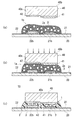
配線基板上にLEDチップをフリップチップ実装する方法としては、図3(a)〜(c)に示すように、従来、種々のものが知られている。
In recent years, attention has been paid to optical functional elements using LEDs.
As such an optical functional element, flip chip mounting in which an LED chip is directly mounted on a wiring board is performed for miniaturization and the like.
As a method of flip-chip mounting an LED chip on a wiring board, various methods are conventionally known as shown in FIGS.
図3(a)は、ワイヤボンディングによる実装方法である。
図3(a)に示す発光装置101では、LEDチップ103の第1及び第2の電極104、105を上側(配線基板102と反対側)にした状態で、LEDチップ103を配線基板102上にダイボンド接着剤110、111によって固定する。
そして、ボンディングワイヤ106、108によって配線基板102上の第1及び第2のパターン電極107、109とLEDチップ103の第1及び第2の電極104、105をそれぞれ電気的に接続する。
FIG. 3A shows a mounting method by wire bonding.
In the
Then, the first and
図3(b)は、導電性ペーストによる実装方法である。
図3(b)に示す発光装置121では、LEDチップ103の第1及び第2の電極104、105を配線基板102側に向けた状態で、これら第1及び第2の電極104、105と配線基板102の第1及び第2のパターン電極124、125とを、例えば銅ペースト等の導電性ペースト122、123によって電気的に接続するとともに、封止樹脂126、127によってLEDチップ103を配線基板102上に接着する。
FIG. 3B shows a mounting method using a conductive paste.
In the
図3(c)は、異方性導電接着剤による実装方法である。
図3(c)に示す発光装置131では、LEDチップ103の第1及び第2の電極104、105を配線基板102側に向けた状態で、これら第1及び第2の電極104、105と、配線基板102の第1及び第2のパターン電極124、125上に設けたバンプ132、133とを、異方性導電接着剤134中の導電性粒子135によって電気的に接続するとともに、異方性導電接着剤134中の絶縁性接着剤樹脂136によってLEDチップ103を配線基板102上に接着する。
FIG. 3C shows a mounting method using an anisotropic conductive adhesive.
In the
しかしながら、上述した従来技術には、種々の課題がある。
まず、ワイヤボンディングによる実装方法においては、金からなるボンディングワイヤ106、108が例えば波長が400〜500nmの光を吸収するため、発光効率が低下してしまう。
また、この方法の場合、オーブンを用いてダイボンド接着剤110、111を硬化させるため、硬化時間が長く、生産効率を向上させることが困難である。
However, the above-described prior art has various problems.
First, in the mounting method by wire bonding, since the
In this method, since the
一方、導電性ペースト122、123を用いる実装方法では、導電性ペースト122、123のみの接着力は弱く、封止樹脂126、127による補強が必要となるが、この封止樹脂126、127により、導電性ペースト122、123内へ光が拡散したり、導電性ペースト122、123内において光が吸収されることにより、発光効率が低下してしまう。
また、この方法の場合、オーブンを用いて封止樹脂126、127を硬化させるため、硬化時間が長く、生産効率を向上させることが困難である。
On the other hand, in the mounting method using the
In this method, since the
他方、異方性導電接着剤134を用いる実装方法では、異方性導電接着剤134中の導電性粒子135の色が茶色であるため絶縁性接着剤樹脂136の色も茶色になり、異方性導電接着剤134内において光が吸収されることにより、発光効率が低下してしまう。
On the other hand, in the mounting method using the anisotropic
このような問題を解決するため、光の反射率が高く、電気抵抗が低い銀(Ag)を用いて導電層を形成することによって光の吸収を抑え、発光効率を低下させることのない異方性導電接着剤を提供することも提案されている。 In order to solve such a problem, an anisotropic layer that suppresses light absorption and does not decrease luminous efficiency by forming a conductive layer using silver (Ag) having high light reflectance and low electrical resistance. It has also been proposed to provide a conductive conductive adhesive.
しかし、銀は化学的に不安定な材料であるため、酸化や硫化しやすいという問題があり、また、熱圧着後において、通電を行うことによってマイグレーションが発生し、これにより配線部分の断線や接着剤の劣化による接着強度の低下を引き起こすという問題がある。 However, since silver is a chemically unstable material, there is a problem that it easily oxidizes and sulphides, and after thermocompression, migration occurs due to energization, which causes disconnection and adhesion of the wiring part. There exists a problem of causing the fall of the adhesive strength by deterioration of an agent.
かかる問題を解決するため、例えば特許文献4に記載されているように、反射率、耐食性、耐マイグレーション性に優れたAg系薄膜合金も提案されている。
このAg系薄膜合金を導電性粒子の表面に被覆すれば、耐食性、耐マイグレーション性は向上するが、このAg系薄膜合金を最表層に用い、下地層に例えばニッケルを用いると、ニッケルの反射率がAgより低いため、導電性粒子全体の反射率が低下してしまうという問題がある。
In order to solve such a problem, for example, as described in Patent Document 4, an Ag-based thin film alloy excellent in reflectance, corrosion resistance, and migration resistance has also been proposed.
If this Ag-based thin film alloy is coated on the surface of the conductive particles, the corrosion resistance and migration resistance will be improved, but if this Ag-based thin film alloy is used as the outermost layer and nickel is used for the underlayer, for example, the reflectance of nickel Is lower than Ag, there is a problem that the reflectivity of the entire conductive particle is lowered.
本発明は、このような従来の技術の課題を考慮してなされたもので、その目的とするところは、銀系金属を導電層とする導電性粒子を用い、光反射率が高く、しかも優れた耐マイグレーション性を有する異方性導電接着剤の技術を提供することにある。 The present invention has been made in consideration of such problems of the conventional technology, and the object of the present invention is to use conductive particles having a silver-based metal as a conductive layer, have high light reflectivity, and be excellent. Another object of the present invention is to provide a technique for an anisotropic conductive adhesive having migration resistance.
上記目的を達成するためになされた本発明は、絶縁性接着剤樹脂中に光反射性の導電性粒子を含有する異方性導電接着剤であって、前記光反射性の導電性粒子が、核となる樹脂粒子の表面に、ピーク波長460nmにおける反射率が60%以上の金属からなる光反射性金属層が形成され、さらに、当該光反射性金属層の表面に銀合金からなる被覆層が形成され、前記光反射性金属層は、当該金属中に銀を98重量%以上含有し、前記被覆層は、当該金属中に銀を95重量%以上含有し、かつ、当該銀以外に、Bi、Ti、Zr、Hf、V、Nd、Ta、Cr、Mo、W、Fe、Ru、Co、Rh、Ir、Pd、Pt、Cu、Au、Zn、Al、Ga、In、Si、Ge、Snからなる群から選択される1又は2以上の金属を含有するものである。
本発明では、前記被覆層は、Ag:Nd:Cuを98.84〜99.07:0.36〜0.44:0.57〜0.72重量%の範囲で含む場合にも効果的である。
また、本発明は、上述したいずれかの異方性導電接着剤を製造する方法であって、前記光反射性金属層を、めっき法によって形成し、前記被覆層を、スパッタリング法によって形成する工程を有する異方性導電接着剤の製造方法である。
一方、本発明は、絶縁性接着剤樹脂中に光反射性の導電性粒子を含有する異方性導電接着剤を製造する方法であって、前記光反射性の導電性粒子が、核となる樹脂粒子の表面に、ピーク波長460nmにおける反射率が60%以上の金属からなる光反射性金属層が形成され、さらに、当該光反射性金属層の表面に銀合金からなる被覆層が形成されてなり、前記光反射性金属層を、当該金属中に銀を98重量%以上含有するように、めっき法によって形成し、前記被覆層を、当該金属中に銀を95重量%以上含有するように、合金からなるターゲットを用いてスパッタリング法によって形成する工程を有する異方性導電接着剤の製造方法である。
本発明では、前記被覆層は、当該金属中に、前記銀以外に、Bi、Ti、Zr、Hf、V、Nd、Ta、Cr、Mo、W、Fe、Ru、Co、Rh、Ir、Pd、Pt、Cu、Au、Zn、Al、Ga、In、Si、Ge、Snからなる群から選択される1又は2以上の金属を含有する場合にも効果的である。
本発明では、前記被覆層は、Ag:Nd:Cuを98.84〜99.07:0.36〜0.44:0.57〜0.72重量%の範囲で含む場合にも効果的である。
さらに、本発明は、対となる接続電極を有する配線基板と、前記配線基板の対となる接続電極にそれぞれ対応する接続電極を有する発光素子とを備え、上述したいずれかの異方性導電接着剤によって前記発光素子が前記配線基板上に接着され、かつ、当該発光素子の接続電極が、当該異方性導電接着剤の導電性粒子を介して当該配線基板の対応する接続電極に対しそれぞれ電気的に接続されている発光装置である。
さらにまた、本発明は、対となる接続電極を有する配線基板と、前記配線基板の接続電極にそれぞれ対応する接続電極を有する発光素子とを用意し、前記配線基板の接続電極と前記発光素子の接続電極を対向する方向に配置した状態で、当該発光素子と当該発光素子との間に上述したいずれかの異方性導電接着剤を配置し、前記配線基板に対して前記発光素子を熱圧着する工程を有する発光素子の製造方法である。
The present invention made to achieve the above object is an anisotropic conductive adhesive containing light reflective conductive particles in an insulating adhesive resin, wherein the light reflective conductive particles are: A light reflective metal layer made of a metal having a reflectance of 60% or more at a peak wavelength of 460 nm is formed on the surface of the resin particle serving as a nucleus, and a coating layer made of a silver alloy is further formed on the surface of the light reflective metal layer. And the light-reflecting metal layer contains 98 wt% or more of silver in the metal, the coating layer contains 95 wt% or more of silver in the metal, and, in addition to the silver, Bi Ti, Zr, Hf, V, Nd, Ta, Cr, Mo, W, Fe, Ru, Co, Rh, Ir, Pd, Pt, Cu, Au, Zn, Al, Ga, In, Si, Ge, Sn Monodea containing one or more metals selected from the group consisting of .
In the present invention, the coating layer is also effective when it contains Ag: Nd: Cu in the range of 98.84 to 99.07: 0.36 to 0.44: 0.57 to 0.72% by weight. is there.
The present invention is also a method for producing any of the above-described anisotropic conductive adhesives, the step of forming the light-reflective metal layer by a plating method and the coating layer by a sputtering method. It is a manufacturing method of the anisotropic conductive adhesive which has.
On the other hand, the present invention is a method for producing an anisotropic conductive adhesive containing light-reflective conductive particles in an insulating adhesive resin, wherein the light-reflective conductive particles serve as a nucleus. A light reflective metal layer made of a metal having a reflectance of 60% or more at a peak wavelength of 460 nm is formed on the surface of the resin particle, and a coating layer made of a silver alloy is formed on the surface of the light reflective metal layer. The light-reflecting metal layer is formed by plating so that the metal contains 98% by weight or more of silver, and the covering layer contains 95% by weight or more of silver in the metal. And a method for producing an anisotropic conductive adhesive having a step of forming by sputtering using a target made of an alloy.
In the present invention, the coating layer includes, in addition to the silver, Bi, Ti, Zr, Hf, V, Nd, Ta, Cr, Mo, W, Fe, Ru, Co, Rh, Ir, Pd in the metal. It is also effective when it contains one or more metals selected from the group consisting of Pt, Cu, Au, Zn, Al, Ga, In, Si, Ge, and Sn.
In the present invention, the coating layer is also effective when it contains Ag: Nd: Cu in the range of 98.84 to 99.07: 0.36 to 0.44: 0.57 to 0.72% by weight. is there.
Furthermore, the present invention includes a wiring board having a pair of connection electrodes, and a light emitting element having a connection electrode corresponding to each of the connection electrodes to be a pair of the wiring boards, and any one of the anisotropic conductive adhesives described above The light emitting element is bonded onto the wiring board by an agent, and the connection electrode of the light emitting element is electrically connected to the corresponding connection electrode of the wiring board through the conductive particles of the anisotropic conductive adhesive. Connected light emitting devices.
Furthermore, the present invention provides a wiring board having a pair of connection electrodes and a light emitting element having a connection electrode corresponding to each of the connection electrodes of the wiring board, and the connection electrode of the wiring board and the light emitting element In a state where the connection electrodes are arranged in the opposing direction, any one of the anisotropic conductive adhesives described above is arranged between the light emitting element and the light emitting element, and the light emitting element is thermocompression bonded to the wiring board. It is a manufacturing method of the light emitting element which has the process to do.
本発明の場合、異方性導電接着剤の導電性粒子が、核となる樹脂粒子の表面に、ピーク波長460nmにおける反射率が60%以上の金属からなる光反射性金属層が形成され、さらに、光反射性金属層の表面に光反射性金属層と同様に反射率の大きい銀合金からなる被覆層が形成されていることから、異方性導電接着剤による光の吸収を最小限に抑えることができる。
その結果、本発明の異方性導電接着剤を用いて配線基板上に発光素子を実装すれば、発光素子の発光効率を低下させることがなく、効率良く光を取り出すことが可能な発光装置を提供することができる。
また、本発明の異方性導電接着剤は、光反射性金属層の表面にマイグレーションの起こりにくい銀合金からなる被覆層が形成されていることから、耐マイグレーション性を向上させることができる。
一方、本発明の方法によれば、異方性導電接着剤の配置と熱圧着工程という簡素で迅速な工程により、上述した顕著な効果を奏する発光装置を製造することができるので、生産効率を大幅に向上させることができる。
In the case of the present invention, a light-reflective metal layer made of a metal having a reflectance at a peak wavelength of 460 nm of 60% or more is formed on the surface of resin particles that are the conductive particles of the anisotropic conductive adhesive. Since the surface of the light reflective metal layer is formed with a coating layer made of a silver alloy having a high reflectance like the light reflective metal layer, the absorption of light by the anisotropic conductive adhesive is minimized. be able to.
As a result, a light emitting device capable of efficiently extracting light without reducing the light emission efficiency of the light emitting element by mounting the light emitting element on the wiring board using the anisotropic conductive adhesive of the present invention. Can be provided.
In addition, the anisotropic conductive adhesive of the present invention can improve the migration resistance because the coating layer made of a silver alloy that hardly causes migration is formed on the surface of the light reflective metal layer.
On the other hand, according to the method of the present invention, it is possible to manufacture a light emitting device that exhibits the above-described remarkable effects by a simple and quick process of arranging an anisotropic conductive adhesive and a thermocompression bonding process. It can be greatly improved.
本発明によれば、銀系金属を導電層とする導電性粒子を用い、光反射率が高く、しかも優れた耐マイグレーション性を有する異方性導電接着剤の技術を提供することができる。 ADVANTAGE OF THE INVENTION According to this invention, the technique of the anisotropic conductive adhesive which uses the electroconductive particle which uses a silver-type metal as a conductive layer, has high light reflectivity, and has the outstanding migration resistance can be provided.
以下、本発明の好ましい実施の形態を図面を参照して詳細に説明する。
なお、本発明は、特にペースト状の異方導電性接着剤が好ましく適用することができるものである。
Hereinafter, preferred embodiments of the present invention will be described in detail with reference to the drawings.
In the present invention, in particular, a paste-like anisotropic conductive adhesive can be preferably applied.
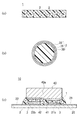
図1(a)は、本発明に係る異方性導電接着剤の構成を模式的に示す断面図、図1(b)は、本発明に用いる導電性粒子の構成を示す拡大断面図、図1(c)は、本発明に係る発光装置の実施の形態の構成を示す断面図である。 1A is a cross-sectional view schematically showing the configuration of the anisotropic conductive adhesive according to the present invention, and FIG. 1B is an enlarged cross-sectional view showing the configuration of the conductive particles used in the present invention. 1 (c) is a cross-sectional view showing a configuration of an embodiment of a light emitting device according to the present invention.
図1(a)に示すように、本発明の異方性導電接着剤1は、絶縁性接着剤樹脂2中に、複数の導電性粒子3が分散された状態で含有してなるものである。
本発明の場合、絶縁性接着剤樹脂2としては、特に限定されることはないが、透明性、接着性、耐熱性、機械的強度、電気絶縁性に優れる観点からは、エポキシ系樹脂と、その硬化剤とを含む組成物を好適に用いることができる。
エポキシ系樹脂は、具体的には、脂環式エポキシ化合物や複素環式エポキシ化合物や水素添加エポキシ化合物などである。脂環式エポキシ化合物としては、分子内に2つ以上のエポキシ基を有するものが好ましく挙げられる。これらは液状であっても、固体状であってもよい。具体的には、グリシジルヘキサヒドロビスフェノールA、3,4−エポキシシクロヘキセニルメチル−3',4'−エポキシシクロヘキセンカルボキシレート等を挙げることができる。中でも、硬化物にLED素子の実装等に適した光透過性を確保でき、速硬化性にも優れている点から、グリシジルヘキサヒドロビスフェノールA、3,4−エポキシシクロヘキセニルメチル−3',4'−エポキシシクロヘキセンカルボキシレートを好ましく使用することができる。
複素環系エポキシ化合物としては、トリアジン環を有するエポキシ化合物を挙げることができ、特に好ましくは1,3,5−トリス(2,3−エポキシプロピル)−1,3,5−トリアジン−2,4,6−(1H,3H,5H)−トリオンを挙げることができる。
水素添加エポキシ化合物としては、先述の脂環式エポキシ化合物や複素環式エポキシ化合物の水素添加物や、その他公知の水素添加エポキシ樹脂を使用することができる。
また、これらのエポキシ化合物に加えて本発明の効果を損なわない限り、他のエポキシ樹脂を併用してもよい。例えば、ビスフェノールA、ビスフェノールF、ビスフェノールS、テトラメチルビスフェノールA、ジアリールビスフェノールA、ハイドロキノン、カテコール、レゾルシン、クレゾール、テトラブロモビスフェノールA、トリヒドロキシビフェニル、ベンゾフェノン、ビスレゾルシノール、ビスフェノールヘキサフルオロアセトン、テトラメチルビスフェノールA、テトラメチルビスフェノールF、トリス(ヒドロキシフェニル)メタン、ビキシレノール、フェノールノボラック、クレゾールノボラックなどの多価フェノールとエピクロルヒドリンとを反応させて得られるグリシジルエーテル1グリセリン、ネオペンチルグリコール、エチレングリコール、プロピレングリコール、チレングリコール、ヘキシレングリコール、ポリエチレングリコール、ポリプロピレングリコールなどの脂肪族多価アルコールとエピクロルヒドリンとを反応させて得られるポリグリシジルエーテルlp−オキシ安息香酸、β−オキシナフトエ酸のようなヒドロキシカルボン酸とエピクロルヒドリンとを反応させて得られるグリシジルエーテルエステル1フタル酸、メチルフタル酸、イソフタル酸、テレフタル酸、テトラハイドロフタル酸、エンドメチレンテトラハイドロフタル酸、エンドメチレンヘキサハイドロフタル酸、トリメリット酸、重合脂肪酸のようなポリカルボン酸から得られるポリグリシジルエステル1アミノフェノール、アミノアルキルフェノールから得られるグリシジルアミノグリシジルエーテル1アミノ安息香酸から得られるグリシジルアミノグリシジルエステル1アニリン、トルイジン、トリブロムアニリン、キシリレンジアミン、ジアミノシクロヘキサン、ビスアミノメチルシクロヘキサン、4,4'−ジアミノジフェニルメタン、4,4'−ジアミノジフェニルスルホンなどから得られるグリシジルアミン1エポキシ化ポリオレフィン等の公知のエポキシ樹脂類が挙げられる。
また、硬化剤としては、酸無水物、イミダゾール化合物、ジシアンなどを挙げることができる。中でも、硬化剤を変色させ難い酸無水物、特に脂環式酸無水物系硬化剤を好ましく使用することができる。具体的には、メチルヘキサヒドロフタル酸無水物等を好ましく挙げることができる。
なお、脂環式のエポキシ化合物と脂環式酸無水物系硬化剤とを使用する場合、それぞれの使用量は、脂環式酸無水物形硬化剤が少なすぎると未硬化エポキシ化合物が多くなり、多すぎると余剰の硬化剤の影響で被着体材料の腐食が促進される傾向があるので、脂環式エポキシ化合物100質量部に対し、好ましくは80〜120質量部、より好ましくは95〜105質量部の割合で使用することができる。
As shown in FIG. 1 (a), the anisotropic
In the case of the present invention, the insulating
Specifically, the epoxy resin is an alicyclic epoxy compound, a heterocyclic epoxy compound, a hydrogenated epoxy compound, or the like. Preferred examples of the alicyclic epoxy compound include those having two or more epoxy groups in the molecule. These may be liquid or solid. Specific examples include glycidyl hexahydrobisphenol A, 3,4-epoxycyclohexenylmethyl-3 ′, 4′-epoxycyclohexene carboxylate, and the like. Among them, glycidyl hexahydrobisphenol A, 3,4-epoxycyclohexenylmethyl-3 ′, 4 is preferable because it can ensure light transmission suitable for mounting LED elements on the cured product and is excellent in rapid curing. '-Epoxycyclohexenecarboxylate can be preferably used.
Examples of the heterocyclic epoxy compound include an epoxy compound having a triazine ring, and 1,3,5-tris (2,3-epoxypropyl) -1,3,5-triazine-2,4 is particularly preferable. , 6- (1H, 3H, 5H) -trione.
As the hydrogenated epoxy compound, hydrogenated products of the above-described alicyclic epoxy compounds and heterocyclic epoxy compounds, and other known hydrogenated epoxy resins can be used.
In addition to these epoxy compounds, other epoxy resins may be used in combination as long as the effects of the present invention are not impaired. For example, bisphenol A, bisphenol F, bisphenol S, tetramethylbisphenol A, diarylbisphenol A, hydroquinone, catechol, resorcin, cresol, tetrabromobisphenol A, trihydroxybiphenyl, benzophenone, bisresorcinol, bisphenol hexafluoroacetone, tetramethylbisphenol G,
Examples of the curing agent include acid anhydrides, imidazole compounds, and dicyan. Among these, acid anhydrides that are difficult to discolor the curing agent, particularly alicyclic acid anhydride curing agents, can be preferably used. Specifically, methylhexahydrophthalic anhydride etc. can be mentioned preferably.
In addition, when using an alicyclic epoxy compound and an alicyclic acid anhydride-based curing agent, the amount of each used increases the amount of uncured epoxy compound if there is too little alicyclic acid anhydride type curing agent. If the amount is too large, corrosion of the adherend material tends to be accelerated due to the influence of the excess curing agent. It can be used at a ratio of 105 parts by mass.
本発明の導電性粒子3は、核となる樹脂粒子30を有し、この樹脂粒子30の表面に、光反射性金属層31が形成され、さらに、光反射性金属層31の表面に銀合金からなる被覆層32が形成されて構成されている。
The
本発明の場合、樹脂粒子30は、特に限定されることはないが、高い導通信頼性を得る観点からは、例えば架橋ポリスチレン系、ベンゾグアナミン系、ナイロン系、PMMA(ポリメタクリレート)系などからなる樹脂粒子を好適に用いることができる。
樹脂粒子30の大きさは、特に限定されることはないが、高い導通信頼性を得る観点からは、平均粒径で3μm〜5μmのものを好適に用いることができる。
In the case of the present invention, the
Although the magnitude | size of the
樹脂粒子30の表面に形成される光反射性金属層31は、青色光のピーク波長であるピーク波長460nmにおける反射率が60%以上、より好ましくは反射率が95%以上の金属材料からなる。
The light-reflective metal layer 31 formed on the surface of the
光反射性金属層31の材料としては、単一の層からなる銀(Ag)、ニッケル(Ni)層表面に金(Au)層が形成されたものがあげられる。 Examples of the material of the light reflective metal layer 31 include a silver (Ag) layer made of a single layer and a nickel (Ni) layer surface on which a gold (Au) layer is formed.
これらのうちでも、反射率をより向上させる観点からは、銀を用いることが好ましい。
この場合、銀としては、純度(金属成分中における割合)が98重量%以上のものを用いることが好ましい。
Among these, it is preferable to use silver from the viewpoint of further improving the reflectance.
In this case, it is preferable to use silver having a purity (ratio in the metal component) of 98% by weight or more.
本発明の場合、光反射性金属層31の形成方法は、特に限定されることはないが、表面を平滑にして反射率をより向上させる観点からは、めっき法を採用することが好ましい。 In the present invention, the method for forming the light-reflective metal layer 31 is not particularly limited, but it is preferable to employ a plating method from the viewpoint of further improving the reflectance by smoothing the surface.
本発明の場合、光反射性金属層31の厚さは特に限定されることはないが、所望の反射率を確保する観点からは、0.05μm以上に設定することが好ましい。
光反射性金属層31の表面に形成される被覆層32は、銀を主体とする合金(本明細書では、「銀合金」という。)からなるものである。
In the present invention, the thickness of the light reflective metal layer 31 is not particularly limited, but is preferably set to 0.05 μm or more from the viewpoint of securing a desired reflectance.
The
本発明の場合、被覆層32の銀合金は、金属中における銀の割合が95重量%以上のものを用いることが好ましい。
この場合、反射率をより向上させる観点からは、光反射性金属層31の金属中における銀の割合が、被覆層32の金属中における割合より大きくなるように構成することが好ましい。
In the case of the present invention, the silver alloy of the
In this case, from the viewpoint of further improving the reflectivity, it is preferable that the ratio of silver in the metal of the light reflective metal layer 31 is larger than the ratio of the
なお、銀合金において、銀の他に含有する金属としては、例えば、Bi、Ti、Zr、Hf、V、Nb、Ta、Cr、Mo、W、Fe、Ru、Co、Rh、Ir、Ni、Pd、Pt、Cu、Au、Zn、Al、Ga、In、Si、Ge、Sn等があげられる。 In addition, in a silver alloy, as a metal contained in addition to silver, for example, Bi, Ti, Zr, Hf, V, Nb, Ta, Cr, Mo, W, Fe, Ru, Co, Rh, Ir, Ni, Pd, Pt, Cu, Au, Zn, Al, Ga, In, Si, Ge, Sn and the like can be mentioned.
そして、本発明の場合、被覆層32の材料としては、青色光のピーク波長であるピーク波長460nmにおける反射率が60%以上、より好ましくは反射率が90%以上の材料からなるものを用いることが好ましい。
In the case of the present invention, the material of the
本発明の場合、被覆層32の形成方法は、特に限定されることはないが、銀合金を均一に被覆する観点からは、スパッタリング法を採用することが好ましい。
In the present invention, the method for forming the
スパッタリング法は、物体に薄膜を形成する方法の一つであり、真空中で行うものである。スパッタリング法では、容器内を真空にした状態で、成膜対象物とスパッタリングターゲットとの間に電圧を印加してグロー放電を生じさせる。これにより発生した電子やイオンが高速でターゲットに衝突することにより、ターゲット材料の粒子が弾き飛ばされ、その粒子(スパッタ粒子)が成膜対象物の表面に付着して薄膜が形成される。
ここで、本発明のような微小な粒子にスパッタリングによって薄膜を形成する方法としては、一次粒子まで分散させた微粒子を装置内の容器にセットし、容器を回転させて微粒子を流動させるとよい。すなわち、このような流動状態の微粒子に対してスパッタリングを行うことにより、各微粒子の全面にターゲット材料のスパッタ粒子が衝突し、各微粒子の全面に薄膜を形成させることができる。
また、本発明に適用するスパッタリング法としては、二極スパッタリング法、マグネトロンスパッタリング法、高周波スパッタリング法、反応性スパッタリング法を含む公知のスパッタリング法を採用することが可能である。
The sputtering method is one of methods for forming a thin film on an object, and is performed in a vacuum. In the sputtering method, a glow discharge is generated by applying a voltage between the film formation target and the sputtering target in a state where the inside of the container is evacuated. Electrons and ions generated thereby collide with the target at a high speed, so that particles of the target material are blown off, and the particles (sputtered particles) adhere to the surface of the film formation target to form a thin film.
Here, as a method of forming a thin film by sputtering on fine particles as in the present invention, fine particles dispersed up to primary particles are set in a container in the apparatus, and the fine particles are flowed by rotating the container. That is, by sputtering the fine particles in such a fluid state, the sputtered particles of the target material collide with the entire surface of each fine particle, and a thin film can be formed on the entire surface of each fine particle.
In addition, as a sputtering method applied to the present invention, known sputtering methods including a bipolar sputtering method, a magnetron sputtering method, a high frequency sputtering method, and a reactive sputtering method can be employed.
本発明の場合、被覆層32の厚さは特に限定されることはないが、所望の耐マイグレーション性を確保する観点からは、0.07μm以上に設定することが好ましい。
In the present invention, the thickness of the
本発明の場合、絶縁性接着剤樹脂2に対する導電性粒子3の含有量は特に限定されることはないが、光反射率、耐マイグレーション性、絶縁性の確保を考慮すると、絶縁性接着剤樹脂2を100重量部に対し、導電性粒子3を1重量部以上100重量部以下含有させることが好ましい。
In the case of the present invention, the content of the
本発明の異方性導電接着剤1を製造するには、例えば、所定のエポキシ樹脂等を溶解させた溶液に、所定の溶剤に分散させた上記導電性粒子3を加えて混合してバインダーペーストを調製する。
In order to produce the anisotropic
ここで、異方性導電接着剤フィルムを製造する場合には、このバインダーペーストを例えばポリエステルフィルム等の剥離フィルム上にコーティングし、乾燥後、カバーフィルムをラミネートして所望の厚さの異方導電性接着フィルムを得る。 Here, when manufacturing an anisotropic conductive adhesive film, this binder paste is coated on a release film such as a polyester film, and after drying, the cover film is laminated and an anisotropic conductive film having a desired thickness is laminated. An adhesive film is obtained.
一方、図1(c)に示すように、本実施の形態の発光装置10は、例えばセラミックスからなる配線基板20と、この配線基板20上に発光素子40が実装されて構成されている。
On the other hand, as shown in FIG. 1C, the
本実施の形態の場合、配線基板20上には、対となる接続電極として、第1及び第2の接続電極21、22が、例えば、銀めっきによって所定のパターン形状に形成されている。
第1及び第2の接続電極21、22の例えば隣接する端部には、例えばスタッドバンプからなる凸状の端子部21b、22bがそれぞれ設けられている。
In the case of the present embodiment, first and
For example, convex
一方、発光素子40としては、例えば、ピーク波長が400nm以上500nm以下の可視光を発光するLED(発光ダイオード)が用いられている。
本発明は、特に、ピーク波長が460nm近傍の青色用のLEDを好適に用いることができる。
On the other hand, as the
In particular, the present invention can suitably use a blue LED having a peak wavelength of around 460 nm.
発光素子40は、その本体部40aが例えば長方体形状に形成され、一方の面上に、アノード電極及びカソード電極である、第1及び第2の接続電極41、42が設けられている。
The
ここで、配線基板20の第1及び第2の接続電極21、22の端子部21b、22bと、発光素子40の第1及び第2の接続電極41、42とは、対向させて配置した場合に、各接続部分が対向するように、それぞれの大きさ並びに形状が設定されている。
そして、発光素子40が、硬化させた上記異方性導電接着剤1によって配線基板20上に接着されている。
Here, the
The
さらに、発光素子40の第1及び第2の接続電極41、42が、異方性導電接着剤1の導電性粒子3を介して配線基板20の対応する第1及び第2の接続電極21、22(端子部21b、22b)に対しそれぞれ電気的に接続されている。
Further, the first and
すなわち、発光素子40の第1の接続電極41が、導電性粒子3の接触によって配線基板20の第1の接続電極21の端子部21bに対し電気的に接続されるとともに、発光素子40の第2の接続電極42が、導電性粒子3の接触によって配線基板20の第2の接続電極22の端子部22bに対し電気的に接続されている。
That is, the
その一方で、配線基板20の第1の接続電極21及び発光素子40の第1の接続電極41と、配線基板20の第2の接続電極22及び発光素子40の第2の接続電極42とは、異方性導電接着剤1中の絶縁性接着剤樹脂2によって互いに絶縁されている。
On the other hand, the
図2(a)〜(c)は、本発明の発光装置の製造工程の実施の形態を示す図である。
まず、図2(a)に示すように、対となる第1及び第2の接続電極21、22を有する配線基板20と、配線基板20の第1及び第2の接続電極21、22にそれぞれ対応する第1及び第2の接続電極41、42を有する発光素子40とを用意する。
2A to 2C are diagrams showing an embodiment of a manufacturing process of the light emitting device of the present invention.
First, as shown in FIG. 2A, the
そして、配線基板20の第1及び第2の接続電極21、22の端子部21b、22bと、発光素子40の第1及び第2の接続電極41、42とを、対向する方向に配置した状態で、配線基板20の第1及び第2の接続電極21、22の端子部21b、22bを覆うように未硬化のペースト状の異方性導電接着剤1aを配置する。
And the state which has arrange | positioned the
なお、例えば未硬化の異方性導電接着剤1aがフィルム状のものである場合には、例えば図示しない貼付装置によって未硬化の異方性導電接着剤1aを、配線基板20の第1及び第2の接続電極21、22が設けられた側の面の所定位置に貼り付ける。
For example, when the uncured anisotropic conductive adhesive 1a is in the form of a film, the uncured anisotropic conductive adhesive 1a is removed from the first and
そして、図2(b)に示すように、未硬化の異方性導電接着剤1a上に発光素子40を載置し、図示しない熱圧着ヘッドによって発光素子40の発光側の面、すなわち、第1及び第2の接続電極41、42が設けられた側と反対側の面40bに対して所定の圧力及び温度で加圧・加熱を行う。
Then, as shown in FIG. 2B, the
これにより、未硬化の異方性導電接着剤1aの絶縁性接着剤樹脂2aが硬化し、図2(c)に示すように、その接着力によって発光素子40が配線基板20上に接着固定される。
As a result, the insulating
また、この熱圧着工程において、配線基板20の第1及び第2の接続電極21、22の端子部21b、22bと、発光素子40の第1及び第2の接続電極41、42とに複数の導電性粒子3がそれぞれ接触して加圧され、その結果、発光素子40の第1の接続電極41と配線基板20の第1の接続電極21、並びに、発光素子40の第2の接続電極42と配線基板20の第2の接続電極22が、それぞれ電気的に接続される。
In this thermocompression bonding step, a plurality of
その一方で、配線基板20の第1の接続電極21及び発光素子40の第1の接続電極41と、配線基板20の第2の接続電極22及び発光素子40の第2の接続電極42とは、異方性導電接着剤1中の絶縁性接着剤樹脂2によって互いに絶縁された状態になる。
そして、以上の工程により、目的とする発光装置10が得られる。
On the other hand, the
And the target light-emitting
以上述べた本実施の形態によれば、異方性導電接着剤1の導電性粒子3が、核となる樹脂粒子30の表面に、ピーク波長460nmにおける反射率が60%以上の金属からなる光反射性金属層31が形成され、さらに、光反射性金属層31の表面に光反射性金属層31と同様に反射率の大きい銀合金からなる被覆層32が形成されていることから、異方性導電接着剤1による光の吸収を最小限に抑えることができる。
According to the present embodiment described above, the
その結果、本発明の異方性導電接着剤1を用いて配線基板20上に発光素子40を実装すれば、発光素子40の発光効率を低下させることがなく、効率良く光を取り出すことが可能な発光装置10を提供することができる。
As a result, if the
また、本発明の異方性導電接着剤1は、光反射性金属層31の表面にマイグレーションの起こりにくい銀合金からなる被覆層32が形成されていることから、耐マイグレーション性を向上させることができる。
Further, the anisotropic
一方、本発明の方法によれば、異方性導電接着剤1の配置工程と、熱圧着工程という簡素で迅速な工程により、発光装置10を製造することができるので、生産効率を大幅に向上させることができる。
On the other hand, according to the method of the present invention, the
なお、本発明は上述した実施の形態に限られることなく、種々の変更を行うことができる。
例えば、図1(c)及び図2(c)に示す発光装置10は、その形状や大きさを簡略化して模式的に示したもので、配線基板並びに発光素子の接続電極の形状、大きさ及び数等については、適宜変更することができる。
The present invention is not limited to the above-described embodiment, and various changes can be made.
For example, the
また、本発明は例えばピーク波長が460nm近傍の青色用の発光素子のみならず、種々のピーク波長を有する発光素子に適用することができる。
ただし、本発明は、ピーク波長が460nm近傍の発光素子に適用した場合に最も効果があるものである。
Further, the present invention can be applied not only to a blue light emitting element having a peak wavelength of around 460 nm, but also to light emitting elements having various peak wavelengths.
However, the present invention is most effective when applied to a light emitting device having a peak wavelength of around 460 nm.
以下、実施例及び比較例を挙げて本発明を具体的に説明するが、本発明は以下の実施例に限定されるものではない。 EXAMPLES Hereinafter, although an Example and a comparative example are given and this invention is demonstrated concretely, this invention is not limited to a following example.
<接着剤組成物の調製>
エポキシ樹脂(日産化学工業社製 TEPIC)50重量部、硬化剤としてメチルヘキサヒドロフタル酸無水物(新日本理化社製 MH−700)50重量部、硬化促進剤(四国化学社製 2E4MZ)2重量部及び溶剤であるトルエンを用いて接着剤組成物を調製した。
<Preparation of adhesive composition>
50 parts by weight of an epoxy resin (TEPIC manufactured by Nissan Chemical Industries, Ltd.), 50 parts by weight of methylhexahydrophthalic anhydride (MH-700 manufactured by Shin Nippon Chemical Co., Ltd.) as a curing agent, 2 parts by weight of a curing accelerator (2E4MZ manufactured by Shikoku Chemicals) An adhesive composition was prepared using parts and toluene as a solvent.
<導電性粒子の作成>
〔実施例粒子1〕
平均粒径5μmの架橋アクリル樹脂からなる樹脂粒子(根上工業社製 アートパール J−6P)の表面に、無電解めっき法により、厚さ0.3μmの銀(Ag)からなる光反射性金属層を形成した。
この場合、めっき液としては、(上村工業社製 プレサRGA−14)を用いた。
この光反射性金属層の表面に、スパッタリング法により、厚さ0.13μmの銀合金からなる被覆層を形成した。
この場合、スパッタリング装置としては、共立社製の粉体スパッタリング装置を用い、スパッタターゲットとしては、溶解、鋳造法により作製したAg・Nd・Cu合金ターゲットを用いた。
このAg・Nd・Cu合金ターゲットは、Ag:Nd:Cuを98.84〜99.07:0.36〜0.44:0.57〜0.72重量%の範囲で含むものである。
<Creation of conductive particles>
[Example particle 1]
A light- reflective metal layer made of silver (Ag) having a thickness of 0.3 μm on the surface of resin particles made of a cross-linked acrylic resin having an average particle size of 5 μm (Art Pearl J-6P manufactured by Negami Kogyo Co., Ltd.) by electroless plating. Formed.
In this case, (Puresa RGA-14 manufactured by Uemura Kogyo Co., Ltd.) was used as the plating solution.
A coating layer made of a silver alloy having a thickness of 0.13 μm was formed on the surface of the light reflective metal layer by sputtering.
In this case, as the sputtering apparatus, using a powder sputtering equipment made co Tatsusha, is as a sputtering target, dissolved, using an Ag · Nd · Cu alloy target prepared by casting method.
This Ag · Nd · Cu alloy target contains Ag: Nd: Cu in the range of 98.84 to 99.07: 0.36 to 0.44: 0.57 to 0.72% by weight.
〔実施例粒子2〕
樹脂粒子の表面に、無電解めっき法により、ニッケル/金からなる厚さ0.13μmの光反射性金属層を形成した。また、銀合金からなる被覆層の厚さを0.4μmとした。それ以外は実施例粒子1と同一の条件で実施例粒子2を作成した。
[Example particle 2]
A light- reflective metal layer made of nickel / gold with a thickness of 0.13 μm was formed on the surface of the resin particles by electroless plating. Further, the thickness of the coating layer made of the silver alloy was set to 0.4 μm. Except that,
〔実施例粒子3〕
ニッケル/金からなる被覆層の厚さを0.13μmとした以外は実施例粒子2と同一の条件で実施例粒子3を作成した。
[Example particle 3]
〔実施例粒子4〕
銀合金からなる被覆層の厚さを0.05μmとした以外は実施例粒子1と同一の条件で実施例粒子4を作成した。
[Example particle 4]
Example particle 4 was prepared under the same conditions as
〔実施例粒子5〕
樹脂粒子の表面に、無電解めっき法によってニッケルのみからなる光反射性層金属層を形成した以外は実施例粒子3と同一の条件で実施例粒子5を作成した。
[Example particle 5]
Example particle 5 was produced under the same conditions as
〔比較例粒子1〕
樹脂粒子の表面に無電解めっき法によって銀からなる光反射性金属層を形成する一方で、被覆層は形成せず、その他は実施例粒子1と同一の条件で比較例粒子1を作成した。
[Comparative Example Particle 1]
While the light-reflective metal layer made of silver was formed on the surface of the resin particle by electroless plating, the coating layer was not formed, and the other
〔比較例粒子2〕
厚さ0.3μmの金(Au)からなる被覆層を形成した以外は実施例粒子5と同一の条件で比較例粒子2を作成した。
[Comparative Example Particle 2]
〔比較例粒子3〕
樹脂粒子の表面に、ニッケルからなるめっきを施す一方で、被覆層を形成せず、その他は実施例粒子1と同一の条件で比較例粒子3を作成した。
[Comparative Example Particle 3]
The surface of the resin particles was plated with nickel, while the coating layer was not formed, and the other
<異方性導電接着剤の作成>
上述した接着剤組成物100重量部(溶剤を除く)に対して上述した実施例粒子1〜5及び比較例粒子1〜3をそれぞれ15重量部混入して、実施例1〜5並びに比較例1〜3の異方性導電接着剤を得た。
<Creation of anisotropic conductive adhesive>
Examples 1 to 5 and Comparative Example 1 were mixed with 15 parts by weight of each of the above-described
<評価>
(1)反射率
実施例1〜5及び比較例1〜3の異方性導電接着剤を平滑な板上に乾燥後の厚さが70μmとなるように塗布し、硬化させて反射率測定用のサンプルを作成した。
各サンプルについて、分光測色計(コニカミノルタ社製 CM−3600d)を用い、青色波長である波長460nmにおける反射率を測定した。その結果を表1に示す。
<Evaluation>
(1) Reflectance The anisotropic conductive adhesives of Examples 1 to 5 and Comparative Examples 1 to 3 were applied on a smooth plate so that the thickness after drying was 70 μm, and cured to reflect the reflectance. A sample was created.
About each sample, the reflectance in wavelength 460nm which is a blue wavelength was measured using the spectrocolorimeter (Konica Minolta company make CM-3600d). The results are shown in Table 1.
(2)耐マイグレーション性
実施例1〜5及び比較例1〜3の異方性導電接着剤を用い、セラミックからなる基板上にLED素子(0.35×0.35mm□)を接着固定(フィリップチップ実装)し、LED素子実装モジュールを作成した。
作成したLED実装モジュールに対し、それぞれ温度85℃、相対湿度85%RHの環境下で通電させる高温高湿試験を、100時間、500時間行い、それぞれの外観を顕微鏡で目視観察した。その結果を表1に示す。
ここでは、異方性導電接着剤中にデンドライト(樹状に延びる析出物)が発生しなかった場合は「○」、デンドライトの発生が認められた場合は「△」とした。
(2) Migration resistance Using the anisotropic conductive adhesives of Examples 1 to 5 and Comparative Examples 1 to 3, an LED element (0.35 × 0.35 mm □) is bonded and fixed on a ceramic substrate (Philip). Chip mounting) to produce an LED element mounting module.
A high-temperature and high-humidity test in which the LED mounting module thus prepared was energized in an environment of a temperature of 85 ° C. and a relative humidity of 85% RH was conducted for 100 hours and 500 hours, and the appearance of each was visually observed with a microscope. The results are shown in Table 1.
Here, when no dendrite (dendritic precipitate) was generated in the anisotropic conductive adhesive, “◯” was indicated, and when dendrite was observed, “Δ”.
(3)導通信頼性
上述した耐マイグレーション性試験において、100時間、500時間、1000時間ごとに電気測定を行いカーブトレーサー(國洋電機工業社製 TCT−2004)によりVf値を測定するとともに、導通の破断(オープン)の有無、短絡発生の有無を確認した。すなわち、導通の破断が確認できた場合は「○」として評価し、測定パターンの一部がショートした場合を「△」として評価した。その結果を表1に示す。
(3) Conduction reliability In the migration resistance test described above, electrical measurement is performed every 100 hours, 500 hours, and 1000 hours, and the Vf value is measured by a curve tracer (TCT-2004, manufactured by Kuniyo Denki Kogyo Co., Ltd.). The presence or absence of breakage (opening) and the presence or absence of a short circuit were confirmed. That is, when the rupture of conduction was confirmed, it was evaluated as “◯”, and when a part of the measurement pattern was short-circuited, “Δ” was evaluated. The results are shown in Table 1.

<実施例1>
表1から明らかなように、実施例1の異方性導電接着剤を用いた樹脂硬化物は、反射率が38%を示し、比較例1に示される、純銀の光反射性金属層上に被覆層を設けない導電性粒子を用いたものと同等の値を示した。
また、実施例1の異方性導電接着剤を用いて作成したLED素子実装モジュールの外観を観察したところ、500時間の高温高湿試験後においてデンドライトは確認されず、耐マイグレーション性も良好であった。
さらに、電気特性については初期状態から変化がなく、導通信頼性も良好であった。
<Example 1>
As is clear from Table 1, the cured resin using the anisotropic conductive adhesive of Example 1 showed a reflectance of 38%, and on the pure silver light-reflecting metal layer shown in Comparative Example 1. A value equivalent to that using conductive particles without a coating layer was exhibited.
Further, when the appearance of the LED element mounting module produced using the anisotropic conductive adhesive of Example 1 was observed, no dendrite was confirmed after the high temperature and high humidity test for 500 hours, and the migration resistance was also good. It was.
Furthermore, the electrical characteristics did not change from the initial state, and the conduction reliability was good.
<実施例2>
導電性粒子の光反射性金属層がニッケル/金めっきからなる実施例2の異方性導電接着剤を用いた樹脂硬化物は、反射率が30%を示し、実施例1のものには及ばなかったが、十分実用可能なレベルであった。
また、実施例2の異方性導電接着剤を用いて作成したLED素子実装モジュールの外観観察については、500時間の高温高湿試験後においてデンドライトは確認されず、耐マイグレーション性も良好であった。
さらに、電気特性については初期状態から変化がなく、導通信頼性も良好であった。
<Example 2>
The resin cured product using the anisotropic conductive adhesive of Example 2 in which the light-reflective metal layer of the conductive particles is made of nickel / gold plating has a reflectance of 30%, which is equivalent to that of Example 1. Although it was not, it was a practical level.
Moreover, about the external appearance observation of the LED element mounting module produced using the anisotropic conductive adhesive of Example 2, dendrite was not confirmed after the high temperature high humidity test of 500 hours, and the migration resistance was also favorable. .
Furthermore, the electrical characteristics did not change from the initial state, and the conduction reliability was good.
<実施例3>
導電性粒子の光反射性金属層がニッケル/金めっきからなり、被覆層の厚さが実施例2より薄い実施例3のものは、反射率が24%を示し、実施例1及び実施例2のものには及ばなかったが、実用可能なレベルであった。
また、実施例3の異方性導電接着剤を用いて作成したLED素子実装モジュールの外観観察については、500時間の高温高湿試験後においてデンドライトは確認されず、耐マイグレーション性も良好であった。
さらに、電気特性については初期状態から変化がなく、導通信頼性も良好であった。
<Example 3>
The light-reflective metal layer of the conductive particles is made of nickel / gold plating, and the thickness of the coating layer of Example 3 where the thickness of the coating layer is thinner than that of Example 2 shows a reflectance of 24%. It was not practical, but it was a practical level.
Moreover, about the external appearance observation of the LED element mounting module produced using the anisotropic conductive adhesive of Example 3, a dendrite was not confirmed after the high temperature high humidity test of 500 hours, and the migration resistance was also favorable. .
Furthermore, the electrical characteristics did not change from the initial state, and the conduction reliability was good.
<実施例4>
導電性粒子の光反射性金属層が純銀からなり、被覆層の厚さが実施例1より薄い実施例4のものは、反射率が26%を示し、比較例1に示される最表層が純銀である導電性粒子を用いたものと遜色のない値を示した。
また、実施例4の異方性導電接着剤を用いて作成したLED素子実装モジュールの外観観察については、500時間の高温高湿試験後においてデンドライトは確認されず、耐マイグレーション性も良好であった。
さらに、電気特性については初期状態から変化がなく、導通信頼性も良好であった。
<Example 4>
The light-reflective metal layer of the conductive particles is made of pure silver, and the coating layer of Example 4 whose thickness is thinner than that of Example 1 has a reflectance of 26%, and the outermost layer shown in Comparative Example 1 is pure silver. The value which is inferior to that using the conductive particles is shown.
Moreover, about the external appearance observation of the LED element mounting module produced using the anisotropic conductive adhesive of Example 4, dendrite was not confirmed after the high temperature high humidity test for 500 hours, and the migration resistance was also favorable. .
Furthermore, the electrical characteristics did not change from the initial state, and the conduction reliability was good.
<実施例5>
光反射性層金属層がニッケルからなる導電性粒子を用いた実施例5のものは、反射率が39%で実施例1と同等であったが、500時間の高温高湿試験後における外観観察においてデンドライトが確認された点で、実施例1の方が優れているといえる。
<Example 5>
Those light-reflective layer metal layer of Example 5 using nickel or Ranaru conductive particles, the reflectance was equivalent to that of Example 1 in 39%, after high-temperature and high-humidity test for 500 hours It can be said that Example 1 is superior in that dendrite is confirmed in appearance observation.
<比較例1>
純銀からなる光反射性金属層上に被覆層を設けない導電性粒子を用いた比較例1の異方性導電接着剤は、反射率が40%で最も良好であったが、100時間の高温高湿試験後における外観観察においてデンドライトが確認され、耐マイグレーション性が実施例1〜4のものに比べて劣っていた。
また、導通試験においては、500時間まではショート等が確認されないものの、1000時間になると断線が確認された。
<Comparative Example 1>
The anisotropic conductive adhesive of Comparative Example 1 using conductive particles without a coating layer on a light-reflective metal layer made of pure silver was the best with a reflectance of 40%. Dendrites were confirmed in appearance observation after the high humidity test, and the migration resistance was inferior to those of Examples 1 to 4.
In the continuity test, no short circuit or the like was confirmed until 500 hours, but disconnection was confirmed after 1000 hours.
<比較例2>
導電性粒子の光反射性金属層がニッケルからなり、被覆層が金(Au)からなる比較例2のものは、耐マイグレーション性及び導通信頼性は良好であったが、反射率が18%を示し、実施例1〜5のものに比べて劣っていた。
<Comparative Example 2>
The comparative example 2 in which the light-reflecting metal layer of the conductive particles is made of nickel and the coating layer is made of gold (Au) has good migration resistance and conduction reliability, but the reflectance is 18%. It was inferior to those of Examples 1-5.
<比較例3>
ニッケルからなる光反射性金属層上に被覆層を設けない導電性粒子を用いた比較例3のものは、耐マイグレーション性及び導通信頼性は良好であったが、反射率が15%を示し、実施例1〜5のものに比べて極端に劣っていた。
<Comparative Example 3>
The thing of the comparative example 3 which used the electroconductive particle which does not provide a coating layer on the light-reflective metal layer which consists of nickel had favorable migration resistance and conduction | electrical_connection reliability, but the reflectance showed 15%, It was extremely inferior compared with the thing of Examples 1-5.
以上の結果より、本発明によれば、光反射率が高く、しかも優れた耐マイグレーション性を有する発光素子用の異方性導電接着剤が得られることを実証することができた。 From the above results, according to the present invention, it was proved that an anisotropic conductive adhesive for a light-emitting element having high light reflectance and excellent migration resistance was obtained.
1…異方性導電接着剤
2…絶縁性接着剤樹脂
3…導電性粒子
10…発光装置
20…配線基板
21…第1の接続電極
22…第2の接続電極
30…樹脂粒子
31…光反射性金属層
32…被覆層
40…発光素子
41…第1の接続電極
42…第2の接続電極
DESCRIPTION OF
Claims (8)
前記光反射性の導電性粒子が、核となる樹脂粒子の表面に、ピーク波長460nmにおける反射率が60%以上の金属からなる光反射性金属層が形成され、さらに、当該光反射性金属層の表面に銀合金からなる被覆層が形成され、
前記光反射性金属層は、当該金属中に銀を98重量%以上含有し、
前記被覆層は、当該金属中に銀を95重量%以上含有し、かつ、当該銀以外に、Bi、Ti、Zr、Hf、V、Nd、Ta、Cr、Mo、W、Fe、Ru、Co、Rh、Ir、Pd、Pt、Cu、Au、Zn、Al、Ga、In、Si、Ge、Snからなる群から選択される1又は2以上の金属を含有する異方性導電接着剤。 An anisotropic conductive adhesive containing light-reflective conductive particles in an insulating adhesive resin,
A light reflective metal layer made of a metal having a reflectance of 60% or more at a peak wavelength of 460 nm is formed on the surface of the resin particle serving as a core of the light reflective conductive particles, and the light reflective metal layer coating layer made of a silver alloy is formed on the surface,
The light reflective metal layer contains 98% by weight or more of silver in the metal,
The coating layer contains 95% by weight or more of silver in the metal, and besides the silver, Bi, Ti, Zr, Hf, V, Nd, Ta, Cr, Mo, W, Fe, Ru, Co An anisotropic conductive adhesive containing one or more metals selected from the group consisting of Rh, Ir, Pd, Pt, Cu, Au, Zn, Al, Ga, In, Si, Ge, and Sn .
前記光反射性金属層を、めっき法によって形成し、前記被覆層を、スパッタリング法によって形成する工程を有する異方性導電接着剤の製造方法。 A method for producing the anisotropic conductive adhesive according to claim 1 or 2,
The manufacturing method of the anisotropic conductive adhesive which has the process of forming the said light-reflective metal layer by the plating method, and forming the said coating layer by sputtering method.
前記光反射性の導電性粒子が、核となる樹脂粒子の表面に、ピーク波長460nmにおける反射率が60%以上の金属からなる光反射性金属層が形成され、さらに、当該光反射性金属層の表面に銀合金からなる被覆層が形成されてなり、A light reflective metal layer made of a metal having a reflectance of 60% or more at a peak wavelength of 460 nm is formed on the surface of the resin particle serving as a core of the light reflective conductive particles, and the light reflective metal layer A coating layer made of a silver alloy is formed on the surface of
前記光反射性金属層を、当該金属中に銀を98重量%以上含有するように、めっき法によって形成し、The light-reflecting metal layer is formed by plating so that the metal contains 98% by weight or more of silver,
前記被覆層を、当該金属中に銀を95重量%以上含有するように、合金からなるターゲットを用いてスパッタリング法によって形成する工程を有する異方性導電接着剤の製造方法。The manufacturing method of the anisotropic conductive adhesive which has the process of forming the said coating layer by sputtering method using the target which consists of an alloy so that silver may contain 95 weight% or more in the said metal.
前記配線基板の対となる接続電極にそれぞれ対応する接続電極を有する発光素子とを備え、
請求項1又は2のいずれか1項記載の異方性導電接着剤によって前記発光素子が前記配線基板上に接着され、かつ、当該発光素子の接続電極が、当該異方性導電接着剤の導電性粒子を介して当該配線基板の対応する接続電極に対しそれぞれ電気的に接続されている発光装置。 A wiring board having a pair of connection electrodes;
A light emitting element having connection electrodes corresponding to the connection electrodes to be paired with the wiring board,
The light emitting element is bonded onto the wiring board by the anisotropic conductive adhesive according to claim 1, and the connection electrode of the light emitting element is electrically conductive by the anisotropic conductive adhesive. Light-emitting device that is electrically connected to the corresponding connection electrode of the wiring board through the conductive particles.
前記配線基板の接続電極と前記発光素子の接続電極を対向する方向に配置した状態で、当該発光素子と当該発光素子との間に請求項1又は2のいずれか1項記載の異方性導電接着剤を配置し、
前記配線基板に対して前記発光素子を熱圧着する工程を有する発光素子の製造方法。 Preparing a wiring board having a pair of connection electrodes and a light emitting element having a connection electrode corresponding to each of the connection electrodes of the wiring board;
3. The anisotropic conduction according to claim 1, wherein the connection electrode of the wiring board and the connection electrode of the light emitting element are arranged in a facing direction, and the anisotropic conduction according to claim 1 is between the light emitting element and the light emitting element. Place the glue,
A method for manufacturing a light emitting element, comprising a step of thermocompression bonding the light emitting element to the wiring board.
Priority Applications (7)
| Application Number | Priority Date | Filing Date | Title |
|---|---|---|---|
| JP2011222498A JP5916334B2 (en) | 2011-10-07 | 2011-10-07 | Anisotropic conductive adhesive and manufacturing method thereof, light emitting device and manufacturing method thereof |
| CN201280060251.8A CN104039914B (en) | 2011-10-07 | 2012-10-05 | Anisotropically conducting adhesive and manufacture method, light-emitting device and manufacture method thereof |
| EP12838614.1A EP2765173A4 (en) | 2011-10-07 | 2012-10-05 | Anisotropic conductive adhesive and method for producing same, and light-emitting device and method for producing same |
| KR1020147011209A KR102010103B1 (en) | 2011-10-07 | 2012-10-05 | Anisotropic conductive adhesive and method for producing same, and light-emitting device and method for producing same |
| PCT/JP2012/076011 WO2013051708A1 (en) | 2011-10-07 | 2012-10-05 | Anisotropic conductive adhesive and method for producing same, and light-emitting device and method for producing same |
| TW101136830A TWI559334B (en) | 2011-10-07 | 2012-10-05 | Anisotropic conductive adhesive and method for producing the same, light emitting device and method for producing the same |
| US14/246,618 US20140217450A1 (en) | 2011-10-07 | 2014-04-07 | Anisotropic conductive adhesive and method for manufacturing same, and light-emitting device and method for manufacturing same |
Applications Claiming Priority (1)
| Application Number | Priority Date | Filing Date | Title |
|---|---|---|---|
| JP2011222498A JP5916334B2 (en) | 2011-10-07 | 2011-10-07 | Anisotropic conductive adhesive and manufacturing method thereof, light emitting device and manufacturing method thereof |
Publications (3)
| Publication Number | Publication Date |
|---|---|
| JP2013082784A JP2013082784A (en) | 2013-05-09 |
| JP2013082784A5 JP2013082784A5 (en) | 2014-11-20 |
| JP5916334B2 true JP5916334B2 (en) | 2016-05-11 |
Family
ID=48043861
Family Applications (1)
| Application Number | Title | Priority Date | Filing Date |
|---|---|---|---|
| JP2011222498A Active JP5916334B2 (en) | 2011-10-07 | 2011-10-07 | Anisotropic conductive adhesive and manufacturing method thereof, light emitting device and manufacturing method thereof |
Country Status (7)
| Country | Link |
|---|---|
| US (1) | US20140217450A1 (en) |
| EP (1) | EP2765173A4 (en) |
| JP (1) | JP5916334B2 (en) |
| KR (1) | KR102010103B1 (en) |
| CN (1) | CN104039914B (en) |
| TW (1) | TWI559334B (en) |
| WO (1) | WO2013051708A1 (en) |
Families Citing this family (30)
| Publication number | Priority date | Publication date | Assignee | Title |
|---|---|---|---|---|
| JP5965199B2 (en) * | 2012-04-17 | 2016-08-03 | デクセリアルズ株式会社 | Anisotropic conductive adhesive and manufacturing method thereof, light emitting device and manufacturing method thereof |
| US9269681B2 (en) * | 2012-11-16 | 2016-02-23 | Qualcomm Incorporated | Surface finish on trace for a thermal compression flip chip (TCFC) |
| JP5985414B2 (en) * | 2013-02-19 | 2016-09-06 | デクセリアルズ株式会社 | Anisotropic conductive adhesive, light emitting device, and method of manufacturing anisotropic conductive adhesive |
| WO2014132979A1 (en) * | 2013-02-27 | 2014-09-04 | 日亜化学工業株式会社 | Light emitting device, method for mounting light emitting element, and mounting device for light emitting elements |
| KR20160061339A (en) * | 2013-09-26 | 2016-05-31 | 데쿠세리아루즈 가부시키가이샤 | Light emitting device, anisotropic conductive adhesive and method for manufacturing light emitting device |
| TWI707484B (en) * | 2013-11-14 | 2020-10-11 | 晶元光電股份有限公司 | Light-emitting device |
| JP6324746B2 (en) * | 2014-02-03 | 2018-05-16 | デクセリアルズ株式会社 | Connection body, method for manufacturing connection body, electronic device |
| JP6347635B2 (en) * | 2014-03-19 | 2018-06-27 | デクセリアルズ株式会社 | Anisotropic conductive adhesive |
| WO2016047950A1 (en) * | 2014-09-26 | 2016-03-31 | Seoul Viosys Co., Ltd. | Light emitting device and method of fabricating the same |
| EP3271953B1 (en) * | 2015-05-21 | 2019-05-01 | Goertek Inc. | Transferring method and manufacturing method of micro-led |
| DE102015112967A1 (en) * | 2015-08-06 | 2017-02-09 | Osram Opto Semiconductors Gmbh | Method for producing an optoelectronic component and optoelectronic component |
| JP2017157724A (en) * | 2016-03-02 | 2017-09-07 | デクセリアルズ株式会社 | Display apparatus and manufacturing method of the same, light emitting apparatus, and manufacturing method of the same |
| DE102016106494A1 (en) * | 2016-04-08 | 2017-10-12 | Osram Opto Semiconductors Gmbh | OPTOELECTRONIC COMPONENT AND METHOD FOR MANUFACTURING AN OPTOELECTRONIC COMPONENT |
| KR102555383B1 (en) * | 2016-12-07 | 2023-07-12 | 엘지디스플레이 주식회사 | Lighting apparatus using organic light emitting diode and method of fabricating the same |
| JP7314801B2 (en) * | 2017-12-28 | 2023-07-26 | 株式会社レゾナック | Connection structure and manufacturing method thereof |
| JP7160302B2 (en) * | 2018-01-31 | 2022-10-25 | 三国電子有限会社 | CONNECTED STRUCTURE AND METHOD OF MAKING CONNECTED STRUCTURE |
| JP7046351B2 (en) | 2018-01-31 | 2022-04-04 | 三国電子有限会社 | How to make a connection structure |
| JP7185252B2 (en) | 2018-01-31 | 2022-12-07 | 三国電子有限会社 | Method for producing connection structure |
| JP7093639B2 (en) * | 2018-02-06 | 2022-06-30 | 三菱マテリアル株式会社 | Silver coated resin particles |
| JP6566178B1 (en) * | 2018-03-01 | 2019-08-28 | 住友ベークライト株式会社 | Paste adhesive composition and semiconductor device |
| WO2019167819A1 (en) * | 2018-03-01 | 2019-09-06 | 住友ベークライト株式会社 | Paste adhesive composition and semiconductor device |
| TWI671921B (en) * | 2018-09-14 | 2019-09-11 | 頎邦科技股份有限公司 | Chip package and chip |
| EP3675190B1 (en) | 2018-12-25 | 2023-05-03 | Nichia Corporation | Method of manufacturing light source device and light source device |
| JP7366337B2 (en) * | 2018-12-25 | 2023-10-23 | 日亜化学工業株式会社 | Manufacturing method of light source device and light source device |
| TWI690102B (en) * | 2019-01-04 | 2020-04-01 | 友達光電股份有限公司 | Light emitting apparatus and manufacturing method thereof |
| JP7298256B2 (en) * | 2019-04-11 | 2023-06-27 | 株式会社レゾナック | conductive particles |
| JP7292669B2 (en) * | 2019-04-11 | 2023-06-19 | 株式会社レゾナック | Method for producing conductive particles |
| CN111574937B (en) * | 2020-05-15 | 2021-10-08 | 武汉华星光电半导体显示技术有限公司 | Anisotropic conductive adhesive, display panel and display device |
| DE102021120689A1 (en) * | 2021-08-09 | 2023-02-09 | OSRAM Opto Semiconductors Gesellschaft mit beschränkter Haftung | TRANSFER PROCESSES FOR OPTOELECTRONIC SEMICONDUCTOR COMPONENTS |
| KR20240038495A (en) * | 2022-09-16 | 2024-03-25 | 삼성전자주식회사 | High reflectance anisotropic conductive film and display module including the same |
Family Cites Families (26)
| Publication number | Priority date | Publication date | Assignee | Title |
|---|---|---|---|---|
| JP2933771B2 (en) | 1991-11-25 | 1999-08-16 | 住友ベークライト株式会社 | Epoxy resin composition for optical semiconductor encapsulation |
| JPH07157720A (en) * | 1993-12-03 | 1995-06-20 | Sumitomo Bakelite Co Ltd | Film having anisotropic electrical conductivity |
| JP3284262B2 (en) * | 1996-09-05 | 2002-05-20 | セイコーエプソン株式会社 | Liquid crystal display device and electronic device using the same |
| US6833180B1 (en) * | 1997-07-04 | 2004-12-21 | Nippon Zeon Company, Ltd. | Adhesive for semiconductor part |
| US5990498A (en) * | 1997-09-16 | 1999-11-23 | Polaroid Corporation | Light-emitting diode having uniform irradiance distribution |
| JP2001234152A (en) * | 2000-02-24 | 2001-08-28 | Sumitomo Metal Mining Co Ltd | Conductive adhesive |
| EP2495732A3 (en) * | 2000-08-04 | 2014-04-16 | Sekisui Chemical Co., Ltd. | Conductive fine particles, method for plating fine particles, and substrate structure |
| JP2002260446A (en) * | 2001-02-27 | 2002-09-13 | Sekisui Chem Co Ltd | Conductive fine particle and conductive connecting structure |
| JP2003026763A (en) | 2001-07-13 | 2003-01-29 | New Japan Chem Co Ltd | Epoxy resin composition |
| EP1626400A4 (en) * | 2003-05-22 | 2008-05-14 | Ricoh Kk | Optical recording medium |
| KR100732017B1 (en) * | 2003-06-25 | 2007-06-25 | 히다치 가세고교 가부시끼가이샤 | Circuit connecting material, film-like circuit connecting material using the same, circuit member connecting structure, and method of producing the same |
| DE10347704A1 (en) | 2003-10-14 | 2005-05-12 | Bayer Ag | Process for the preparation of purified elastomers from solution |
| JP4433876B2 (en) * | 2004-05-18 | 2010-03-17 | 住友金属鉱山株式会社 | Epoxy resin composition and adhesive for optical semiconductor using the same |
| CN1989573A (en) * | 2004-08-05 | 2007-06-27 | 积水化学工业株式会社 | Conductive fine particle, method for producing conductive fine particle and electroless silver plating liquid |
| JP4802666B2 (en) * | 2005-11-08 | 2011-10-26 | 住友金属鉱山株式会社 | Epoxy resin adhesive composition and optical semiconductor adhesive using the same |
| JP2007258324A (en) * | 2006-03-22 | 2007-10-04 | Matsushita Electric Ind Co Ltd | Light-emitting device and manufacturing method thereof |
| JP4978286B2 (en) * | 2007-04-16 | 2012-07-18 | ソニー株式会社 | Silver-based thin film alloy |
| JP5430093B2 (en) * | 2008-07-24 | 2014-02-26 | デクセリアルズ株式会社 | Conductive particles, anisotropic conductive film, joined body, and connection method |
| US20120202218A1 (en) * | 2008-09-12 | 2012-08-09 | Modpro Ab | Detection method and device based on nanoparticle aggregation |
| JP5617210B2 (en) * | 2009-09-14 | 2014-11-05 | デクセリアルズ株式会社 | Light-reflective anisotropic conductive adhesive and light-emitting device |
| JP5526698B2 (en) * | 2009-10-16 | 2014-06-18 | デクセリアルズ株式会社 | Light reflective conductive particles, anisotropic conductive adhesive, and light emitting device |
| JP2011186414A (en) * | 2010-02-12 | 2011-09-22 | Sony Corp | Optical device, sun screening apparatus, fitting, window material, and method of producing optical device |
| JP5745776B2 (en) * | 2010-03-15 | 2015-07-08 | デクセリアルズ株式会社 | Optical laminate and joinery |
| JP5586300B2 (en) * | 2010-03-31 | 2014-09-10 | デクセリアルズ株式会社 | Functional laminate and functional structure |
| JP5583613B2 (en) * | 2011-02-04 | 2014-09-03 | 株式会社日本触媒 | Conductive fine particles |
| JP5609716B2 (en) * | 2011-03-07 | 2014-10-22 | デクセリアルズ株式会社 | Light-reflective anisotropic conductive adhesive and light-emitting device |
-
2011
- 2011-10-07 JP JP2011222498A patent/JP5916334B2/en active Active
-
2012
- 2012-10-05 CN CN201280060251.8A patent/CN104039914B/en active Active
- 2012-10-05 EP EP12838614.1A patent/EP2765173A4/en not_active Withdrawn
- 2012-10-05 TW TW101136830A patent/TWI559334B/en active
- 2012-10-05 WO PCT/JP2012/076011 patent/WO2013051708A1/en active Application Filing
- 2012-10-05 KR KR1020147011209A patent/KR102010103B1/en active IP Right Grant
-
2014
- 2014-04-07 US US14/246,618 patent/US20140217450A1/en not_active Abandoned
Also Published As
| Publication number | Publication date |
|---|---|
| KR102010103B1 (en) | 2019-08-12 |
| EP2765173A1 (en) | 2014-08-13 |
| EP2765173A4 (en) | 2015-04-29 |
| TWI559334B (en) | 2016-11-21 |
| US20140217450A1 (en) | 2014-08-07 |
| TW201331955A (en) | 2013-08-01 |
| KR20140084076A (en) | 2014-07-04 |
| WO2013051708A1 (en) | 2013-04-11 |
| CN104039914A (en) | 2014-09-10 |
| JP2013082784A (en) | 2013-05-09 |
| CN104039914B (en) | 2016-08-24 |
Similar Documents
| Publication | Publication Date | Title |
|---|---|---|
| JP5916334B2 (en) | Anisotropic conductive adhesive and manufacturing method thereof, light emitting device and manufacturing method thereof | |
| JP5965199B2 (en) | Anisotropic conductive adhesive and manufacturing method thereof, light emitting device and manufacturing method thereof | |
| JP5985414B2 (en) | Anisotropic conductive adhesive, light emitting device, and method of manufacturing anisotropic conductive adhesive | |
| JP5526698B2 (en) | Light reflective conductive particles, anisotropic conductive adhesive, and light emitting device | |
| JP6292808B2 (en) | Adhesive and light emitting device | |
| CN106062119B (en) | Anisotropically conducting adhesive | |
| JP6066643B2 (en) | Anisotropic conductive adhesive | |
| JP5555038B2 (en) | Light-reflective anisotropic conductive adhesive and light-emitting device | |
| JPWO2012144033A1 (en) | Light reflective conductive particles, anisotropic conductive adhesive, and light emitting device | |
| JP2014160708A (en) | Anisotropic conductive adhesive material, light-emitting device, and method for manufacturing anisotropic conductive adhesive material | |
| JP2014030026A (en) | Anisotropic conducting adhesive material, and light-emitting device | |
| JP5785306B2 (en) | Light-reflective anisotropic conductive adhesive and light-emitting device |
Legal Events
| Date | Code | Title | Description |
|---|---|---|---|
| A521 | Request for written amendment filed |
Free format text: JAPANESE INTERMEDIATE CODE: A821 Effective date: 20141003 Free format text: JAPANESE INTERMEDIATE CODE: A523 Effective date: 20141003 |
|
| A621 | Written request for application examination |
Free format text: JAPANESE INTERMEDIATE CODE: A621 Effective date: 20141003 |
|
| A131 | Notification of reasons for refusal |
Free format text: JAPANESE INTERMEDIATE CODE: A131 Effective date: 20150915 |
|
| A521 | Request for written amendment filed |
Free format text: JAPANESE INTERMEDIATE CODE: A523 Effective date: 20151116 Free format text: JAPANESE INTERMEDIATE CODE: A821 Effective date: 20151116 |
|
| TRDD | Decision of grant or rejection written | ||
| A01 | Written decision to grant a patent or to grant a registration (utility model) |
Free format text: JAPANESE INTERMEDIATE CODE: A01 Effective date: 20160329 |
|
| A61 | First payment of annual fees (during grant procedure) |
Free format text: JAPANESE INTERMEDIATE CODE: A61 Effective date: 20160405 |
|
| R150 | Certificate of patent or registration of utility model |
Ref document number: 5916334 Country of ref document: JP Free format text: JAPANESE INTERMEDIATE CODE: R150 |
|
| R250 | Receipt of annual fees |
Free format text: JAPANESE INTERMEDIATE CODE: R250 |
|
| R250 | Receipt of annual fees |
Free format text: JAPANESE INTERMEDIATE CODE: R250 |
|
| R250 | Receipt of annual fees |
Free format text: JAPANESE INTERMEDIATE CODE: R250 |
|
| R250 | Receipt of annual fees |
Free format text: JAPANESE INTERMEDIATE CODE: R250 |
|
| R250 | Receipt of annual fees |
Free format text: JAPANESE INTERMEDIATE CODE: R250 |
|
| R250 | Receipt of annual fees |
Free format text: JAPANESE INTERMEDIATE CODE: R250 |