US11309688B2 - Nitride semiconductor light-emitting element, method for manufacturing nitride semiconductor light-emitting element, and nitride semiconductor light-emitting device - Google Patents
Nitride semiconductor light-emitting element, method for manufacturing nitride semiconductor light-emitting element, and nitride semiconductor light-emitting device Download PDFInfo
- Publication number
- US11309688B2 US11309688B2 US16/584,173 US201916584173A US11309688B2 US 11309688 B2 US11309688 B2 US 11309688B2 US 201916584173 A US201916584173 A US 201916584173A US 11309688 B2 US11309688 B2 US 11309688B2
- Authority
- US
- United States
- Prior art keywords
- trench
- nitride semiconductor
- semiconductor light
- emitting element
- waveguide
- Prior art date
- Legal status (The legal status is an assumption and is not a legal conclusion. Google has not performed a legal analysis and makes no representation as to the accuracy of the status listed.)
- Active, expires
Links
Images


Classifications
-
- H—ELECTRICITY
- H01—ELECTRIC ELEMENTS
- H01S—DEVICES USING THE PROCESS OF LIGHT AMPLIFICATION BY STIMULATED EMISSION OF RADIATION [LASER] TO AMPLIFY OR GENERATE LIGHT; DEVICES USING STIMULATED EMISSION OF ELECTROMAGNETIC RADIATION IN WAVE RANGES OTHER THAN OPTICAL
- H01S5/00—Semiconductor lasers
- H01S5/30—Structure or shape of the active region; Materials used for the active region
- H01S5/34—Structure or shape of the active region; Materials used for the active region comprising quantum well or superlattice structures, e.g. single quantum well [SQW] lasers, multiple quantum well [MQW] lasers or graded index separate confinement heterostructure [GRINSCH] lasers
- H01S5/343—Structure or shape of the active region; Materials used for the active region comprising quantum well or superlattice structures, e.g. single quantum well [SQW] lasers, multiple quantum well [MQW] lasers or graded index separate confinement heterostructure [GRINSCH] lasers in AIIIBV compounds, e.g. AlGaAs-laser, InP-based laser
- H01S5/34333—Structure or shape of the active region; Materials used for the active region comprising quantum well or superlattice structures, e.g. single quantum well [SQW] lasers, multiple quantum well [MQW] lasers or graded index separate confinement heterostructure [GRINSCH] lasers in AIIIBV compounds, e.g. AlGaAs-laser, InP-based laser with a well layer based on Ga(In)N or Ga(In)P, e.g. blue laser
-
- B—PERFORMING OPERATIONS; TRANSPORTING
- B28—WORKING CEMENT, CLAY, OR STONE
- B28D—WORKING STONE OR STONE-LIKE MATERIALS
- B28D5/00—Fine working of gems, jewels, crystals, e.g. of semiconductor material; apparatus or devices therefor
- B28D5/0005—Fine working of gems, jewels, crystals, e.g. of semiconductor material; apparatus or devices therefor by breaking, e.g. dicing
- B28D5/0011—Fine working of gems, jewels, crystals, e.g. of semiconductor material; apparatus or devices therefor by breaking, e.g. dicing with preliminary treatment, e.g. weakening by scoring
-
- B—PERFORMING OPERATIONS; TRANSPORTING
- B28—WORKING CEMENT, CLAY, OR STONE
- B28D—WORKING STONE OR STONE-LIKE MATERIALS
- B28D5/00—Fine working of gems, jewels, crystals, e.g. of semiconductor material; apparatus or devices therefor
- B28D5/0005—Fine working of gems, jewels, crystals, e.g. of semiconductor material; apparatus or devices therefor by breaking, e.g. dicing
- B28D5/0017—Fine working of gems, jewels, crystals, e.g. of semiconductor material; apparatus or devices therefor by breaking, e.g. dicing using moving tools
- B28D5/0023—Fine working of gems, jewels, crystals, e.g. of semiconductor material; apparatus or devices therefor by breaking, e.g. dicing using moving tools rectilinearly
-
- H—ELECTRICITY
- H01—ELECTRIC ELEMENTS
- H01L—SEMICONDUCTOR DEVICES NOT COVERED BY CLASS H10
- H01L21/00—Processes or apparatus adapted for the manufacture or treatment of semiconductor or solid state devices or of parts thereof
- H01L21/02—Manufacture or treatment of semiconductor devices or of parts thereof
- H01L21/04—Manufacture or treatment of semiconductor devices or of parts thereof the devices having at least one potential-jump barrier or surface barrier, e.g. PN junction, depletion layer or carrier concentration layer
- H01L21/18—Manufacture or treatment of semiconductor devices or of parts thereof the devices having at least one potential-jump barrier or surface barrier, e.g. PN junction, depletion layer or carrier concentration layer the devices having semiconductor bodies comprising elements of Group IV of the Periodic System or AIIIBV compounds with or without impurities, e.g. doping materials
- H01L21/20—Deposition of semiconductor materials on a substrate, e.g. epitaxial growth solid phase epitaxy
-
- H—ELECTRICITY
- H01—ELECTRIC ELEMENTS
- H01L—SEMICONDUCTOR DEVICES NOT COVERED BY CLASS H10
- H01L21/00—Processes or apparatus adapted for the manufacture or treatment of semiconductor or solid state devices or of parts thereof
- H01L21/02—Manufacture or treatment of semiconductor devices or of parts thereof
- H01L21/04—Manufacture or treatment of semiconductor devices or of parts thereof the devices having at least one potential-jump barrier or surface barrier, e.g. PN junction, depletion layer or carrier concentration layer
- H01L21/18—Manufacture or treatment of semiconductor devices or of parts thereof the devices having at least one potential-jump barrier or surface barrier, e.g. PN junction, depletion layer or carrier concentration layer the devices having semiconductor bodies comprising elements of Group IV of the Periodic System or AIIIBV compounds with or without impurities, e.g. doping materials
- H01L21/30—Treatment of semiconductor bodies using processes or apparatus not provided for in groups H01L21/20 - H01L21/26
- H01L21/302—Treatment of semiconductor bodies using processes or apparatus not provided for in groups H01L21/20 - H01L21/26 to change their surface-physical characteristics or shape, e.g. etching, polishing, cutting
- H01L21/306—Chemical or electrical treatment, e.g. electrolytic etching
- H01L21/3065—Plasma etching; Reactive-ion etching
-
- H—ELECTRICITY
- H01—ELECTRIC ELEMENTS
- H01L—SEMICONDUCTOR DEVICES NOT COVERED BY CLASS H10
- H01L33/00—Semiconductor devices with at least one potential-jump barrier or surface barrier specially adapted for light emission; Processes or apparatus specially adapted for the manufacture or treatment thereof or of parts thereof; Details thereof
- H01L33/005—Processes
- H01L33/0062—Processes for devices with an active region comprising only III-V compounds
- H01L33/0075—Processes for devices with an active region comprising only III-V compounds comprising nitride compounds
-
- H—ELECTRICITY
- H01—ELECTRIC ELEMENTS
- H01S—DEVICES USING THE PROCESS OF LIGHT AMPLIFICATION BY STIMULATED EMISSION OF RADIATION [LASER] TO AMPLIFY OR GENERATE LIGHT; DEVICES USING STIMULATED EMISSION OF ELECTROMAGNETIC RADIATION IN WAVE RANGES OTHER THAN OPTICAL
- H01S5/00—Semiconductor lasers
- H01S5/02—Structural details or components not essential to laser action
- H01S5/0201—Separation of the wafer into individual elements, e.g. by dicing, cleaving, etching or directly during growth
- H01S5/0202—Cleaving
-
- H—ELECTRICITY
- H01—ELECTRIC ELEMENTS
- H01S—DEVICES USING THE PROCESS OF LIGHT AMPLIFICATION BY STIMULATED EMISSION OF RADIATION [LASER] TO AMPLIFY OR GENERATE LIGHT; DEVICES USING STIMULATED EMISSION OF ELECTROMAGNETIC RADIATION IN WAVE RANGES OTHER THAN OPTICAL
- H01S5/00—Semiconductor lasers
- H01S5/02—Structural details or components not essential to laser action
- H01S5/026—Monolithically integrated components, e.g. waveguides, monitoring photo-detectors, drivers
-
- H—ELECTRICITY
- H01—ELECTRIC ELEMENTS
- H01S—DEVICES USING THE PROCESS OF LIGHT AMPLIFICATION BY STIMULATED EMISSION OF RADIATION [LASER] TO AMPLIFY OR GENERATE LIGHT; DEVICES USING STIMULATED EMISSION OF ELECTROMAGNETIC RADIATION IN WAVE RANGES OTHER THAN OPTICAL
- H01S5/00—Semiconductor lasers
- H01S5/20—Structure or shape of the semiconductor body to guide the optical wave ; Confining structures perpendicular to the optical axis, e.g. index or gain guiding, stripe geometry, broad area lasers, gain tailoring, transverse or lateral reflectors, special cladding structures, MQW barrier reflection layers
- H01S5/22—Structure or shape of the semiconductor body to guide the optical wave ; Confining structures perpendicular to the optical axis, e.g. index or gain guiding, stripe geometry, broad area lasers, gain tailoring, transverse or lateral reflectors, special cladding structures, MQW barrier reflection layers having a ridge or stripe structure
- H01S5/2202—Structure or shape of the semiconductor body to guide the optical wave ; Confining structures perpendicular to the optical axis, e.g. index or gain guiding, stripe geometry, broad area lasers, gain tailoring, transverse or lateral reflectors, special cladding structures, MQW barrier reflection layers having a ridge or stripe structure by making a groove in the upper laser structure
-
- H—ELECTRICITY
- H01—ELECTRIC ELEMENTS
- H01S—DEVICES USING THE PROCESS OF LIGHT AMPLIFICATION BY STIMULATED EMISSION OF RADIATION [LASER] TO AMPLIFY OR GENERATE LIGHT; DEVICES USING STIMULATED EMISSION OF ELECTROMAGNETIC RADIATION IN WAVE RANGES OTHER THAN OPTICAL
- H01S5/00—Semiconductor lasers
- H01S5/30—Structure or shape of the active region; Materials used for the active region
- H01S5/34—Structure or shape of the active region; Materials used for the active region comprising quantum well or superlattice structures, e.g. single quantum well [SQW] lasers, multiple quantum well [MQW] lasers or graded index separate confinement heterostructure [GRINSCH] lasers
- H01S5/343—Structure or shape of the active region; Materials used for the active region comprising quantum well or superlattice structures, e.g. single quantum well [SQW] lasers, multiple quantum well [MQW] lasers or graded index separate confinement heterostructure [GRINSCH] lasers in AIIIBV compounds, e.g. AlGaAs-laser, InP-based laser
- H01S5/34346—Structure or shape of the active region; Materials used for the active region comprising quantum well or superlattice structures, e.g. single quantum well [SQW] lasers, multiple quantum well [MQW] lasers or graded index separate confinement heterostructure [GRINSCH] lasers in AIIIBV compounds, e.g. AlGaAs-laser, InP-based laser characterised by the materials of the barrier layers
-
- H—ELECTRICITY
- H01—ELECTRIC ELEMENTS
- H01L—SEMICONDUCTOR DEVICES NOT COVERED BY CLASS H10
- H01L21/00—Processes or apparatus adapted for the manufacture or treatment of semiconductor or solid state devices or of parts thereof
- H01L21/02—Manufacture or treatment of semiconductor devices or of parts thereof
- H01L21/04—Manufacture or treatment of semiconductor devices or of parts thereof the devices having at least one potential-jump barrier or surface barrier, e.g. PN junction, depletion layer or carrier concentration layer
- H01L21/18—Manufacture or treatment of semiconductor devices or of parts thereof the devices having at least one potential-jump barrier or surface barrier, e.g. PN junction, depletion layer or carrier concentration layer the devices having semiconductor bodies comprising elements of Group IV of the Periodic System or AIIIBV compounds with or without impurities, e.g. doping materials
- H01L21/28—Manufacture of electrodes on semiconductor bodies using processes or apparatus not provided for in groups H01L21/20 - H01L21/268
- H01L21/283—Deposition of conductive or insulating materials for electrodes conducting electric current
- H01L21/285—Deposition of conductive or insulating materials for electrodes conducting electric current from a gas or vapour, e.g. condensation
- H01L21/28506—Deposition of conductive or insulating materials for electrodes conducting electric current from a gas or vapour, e.g. condensation of conductive layers
- H01L21/28512—Deposition of conductive or insulating materials for electrodes conducting electric current from a gas or vapour, e.g. condensation of conductive layers on semiconductor bodies comprising elements of Group IV of the Periodic System
-
- H—ELECTRICITY
- H01—ELECTRIC ELEMENTS
- H01S—DEVICES USING THE PROCESS OF LIGHT AMPLIFICATION BY STIMULATED EMISSION OF RADIATION [LASER] TO AMPLIFY OR GENERATE LIGHT; DEVICES USING STIMULATED EMISSION OF ELECTROMAGNETIC RADIATION IN WAVE RANGES OTHER THAN OPTICAL
- H01S2304/00—Special growth methods for semiconductor lasers
-
- H—ELECTRICITY
- H01—ELECTRIC ELEMENTS
- H01S—DEVICES USING THE PROCESS OF LIGHT AMPLIFICATION BY STIMULATED EMISSION OF RADIATION [LASER] TO AMPLIFY OR GENERATE LIGHT; DEVICES USING STIMULATED EMISSION OF ELECTROMAGNETIC RADIATION IN WAVE RANGES OTHER THAN OPTICAL
- H01S5/00—Semiconductor lasers
- H01S5/02—Structural details or components not essential to laser action
- H01S5/0206—Substrates, e.g. growth, shape, material, removal or bonding
-
- H—ELECTRICITY
- H01—ELECTRIC ELEMENTS
- H01S—DEVICES USING THE PROCESS OF LIGHT AMPLIFICATION BY STIMULATED EMISSION OF RADIATION [LASER] TO AMPLIFY OR GENERATE LIGHT; DEVICES USING STIMULATED EMISSION OF ELECTROMAGNETIC RADIATION IN WAVE RANGES OTHER THAN OPTICAL
- H01S5/00—Semiconductor lasers
- H01S5/02—Structural details or components not essential to laser action
- H01S5/022—Mountings; Housings
- H01S5/0233—Mounting configuration of laser chips
- H01S5/02345—Wire-bonding
-
- H—ELECTRICITY
- H01—ELECTRIC ELEMENTS
- H01S—DEVICES USING THE PROCESS OF LIGHT AMPLIFICATION BY STIMULATED EMISSION OF RADIATION [LASER] TO AMPLIFY OR GENERATE LIGHT; DEVICES USING STIMULATED EMISSION OF ELECTROMAGNETIC RADIATION IN WAVE RANGES OTHER THAN OPTICAL
- H01S5/00—Semiconductor lasers
- H01S5/04—Processes or apparatus for excitation, e.g. pumping, e.g. by electron beams
- H01S5/042—Electrical excitation ; Circuits therefor
- H01S5/0425—Electrodes, e.g. characterised by the structure
- H01S5/04252—Electrodes, e.g. characterised by the structure characterised by the material
-
- H—ELECTRICITY
- H01—ELECTRIC ELEMENTS
- H01S—DEVICES USING THE PROCESS OF LIGHT AMPLIFICATION BY STIMULATED EMISSION OF RADIATION [LASER] TO AMPLIFY OR GENERATE LIGHT; DEVICES USING STIMULATED EMISSION OF ELECTROMAGNETIC RADIATION IN WAVE RANGES OTHER THAN OPTICAL
- H01S5/00—Semiconductor lasers
- H01S5/10—Construction or shape of the optical resonator, e.g. extended or external cavity, coupled cavities, bent-guide, varying width, thickness or composition of the active region
- H01S5/1053—Comprising an active region having a varying composition or cross-section in a specific direction
- H01S5/1064—Comprising an active region having a varying composition or cross-section in a specific direction varying width along the optical axis
-
- H—ELECTRICITY
- H01—ELECTRIC ELEMENTS
- H01S—DEVICES USING THE PROCESS OF LIGHT AMPLIFICATION BY STIMULATED EMISSION OF RADIATION [LASER] TO AMPLIFY OR GENERATE LIGHT; DEVICES USING STIMULATED EMISSION OF ELECTROMAGNETIC RADIATION IN WAVE RANGES OTHER THAN OPTICAL
- H01S5/00—Semiconductor lasers
- H01S5/20—Structure or shape of the semiconductor body to guide the optical wave ; Confining structures perpendicular to the optical axis, e.g. index or gain guiding, stripe geometry, broad area lasers, gain tailoring, transverse or lateral reflectors, special cladding structures, MQW barrier reflection layers
- H01S5/2004—Confining in the direction perpendicular to the layer structure
- H01S5/2009—Confining in the direction perpendicular to the layer structure by using electron barrier layers
Definitions
- the present disclosure relates to nitride semiconductor light-emitting elements, methods for manufacturing a nitride semiconductor light-emitting element, and nitride semiconductor light-emitting devices, and in particular relates to a watt-class high-output semiconductor light-emitting element used in a projector light source and a headlamp for automobiles.
- projectors have been widely used as projection-type image display devices which project an enlarged optical image obtained using a spatial light modulation element such as a compact liquid-crystal panel that forms an image corresponding to an image signal onto a screen through a projector lens by illuminating the spatial light modulation element by light from a light source such as a lamp.
- the light source generally includes an ultra-high pressure mercury lamp which exhibits high luminescence efficiency in the wavelength range of visible light.
- a light-emitting diode (LED) or a laser which is a semiconductor light-emitting element characterized by high luminance, high definition, low power consumption, a long operational life, etc. have recently begun to be used instead of a high pressure mercury lamp in a light source of a projector.
- a laser projector including a watt-class high-output semiconductor laser as a light source has begun to spread.
- the watt-class high-output semiconductor laser has begun to develop into a light source for vehicle headlamps.
- a light source including a semiconductor light-emitting element such as a laser has been spreading to various fields.
- a waveguide has different widths at one end portion and the other end portion in the cavity length direction.
- a semiconductor laser element including a tapered strip waveguide is known (for example, Japanese Unexamined Patent Application Publication No. 2009-295680).
- Examples of a semiconductor light-emitting element suitable for a light source of a projector include a nitride-based semiconductor laser which uses a nitride-based material.
- a light source that emits blue-violet light in a wavelength range of 405 nm is provided using a nitride-based semiconductor laser, blue phosphor, green phosphor, and red phosphor are excited by laser light emitted from the nitride-based semiconductor layer, and blue light, green light, and red light are emitted from these phosphors; thus, a compact, low power consuming laser projector can be provided.
- the nitride-based semiconductor laser involves splitting along a crystal face other than a cleavage surface upon an element split. Therefore, the high likelihood of problems such as a split out of an element split line or cracking of a laser element in the process of cutting out an individual laser element from a wafer (the process of obtaining a chip) has been an issue.
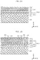
- FIG. 49 is a plan view of semiconductor light-emitting element 1000 according to Conventional Example 1 disclosed in Japanese Unexamined Patent Application Publication No. 2011-029224.
- semiconductor layer stacked body 1200 formed on a substrate includes guide trench 1201 for element splits which extends in the direction of an element split.
- FIG. 50 is a plan view of semiconductor light-emitting element 2000 according to Conventional Example 2 disclosed in Japanese Unexamined Patent Application Publication No. 2007-329459.
- semiconductor layer stacked body 2200 formed on a substrate includes first guide trench 2201 for element splits which is in the form of a projection at a leading end, and further includes a second guide trench 2202 at the bottom of first guide trench 2201 .
- a nitride oxide semiconductor light-emitting element in which the position of a waveguide is offset along the width of the element has been studied, but it is not easy to manufacture, in quantity, a nitride semiconductor light-emitting element in which the position of a waveguide is offset along the width of the element while maintaining a structure in which the waveguide has different widths at one end portion and the other end portion.
- the first purpose of the present disclosure is to provide, for example, a method for manufacturing a nitride semiconductor light-emitting element by which it is possible to easily manufacture, in quantity, a semiconductor laser element in which a waveguide has different widths at one end portion and the other end portion and the position of the waveguide is offset along the width of the element.
- the second purpose of the present disclosure is to provide, for example, a method for manufacturing a nitride semiconductor light-emitting element in which upon an element split, generation of particles can be sufficiently reduced.
- a method for manufacturing a first nitride semiconductor light-emitting element includes: fabricating a semiconductor layer stacked substrate including a semiconductor layer stacked body on a substrate, the semiconductor layer stacked body including a plurality of waveguides extending in a second direction substantially orthogonal to a first direction; fabricating a plurality of bar-shaped substrates by splitting the semiconductor layer stacked substrate along a plurality of first-direction split lines parallel to the first direction, resulting in the plurality of waveguides being cut; and fabricating a plurality of individual elements by splitting each of the plurality of bar-shaped substrates along a plurality of second-direction split lines parallel to the second direction.
- a waveguide in each of the plurality of individual elements has different widths at one end portion and another end portion and a center line of the waveguide is located off a center of the individual element along the first direction
- the semiconductor layer stacked substrate includes a plurality of element forming regions corresponding to the plurality of individual elements, the plurality of element forming regions include a first element forming region and a second element forming region which are adjacent to each other in the second direction, and two of the plurality of second-direction split lines sandwiching the first element forming region and two of the plurality of second-direction split lines sandwiching the second element forming region are misaligned in the first direction.
- a first nitride semiconductor light-emitting element includes: a substrate; and a semiconductor element structure on one surface of the substrate, and the semiconductor element structure includes a waveguide extending in a second direction substantially orthogonal to a first direction.
- the nitride semiconductor light-emitting element has: a first side surface substantially parallel to the second direction; a second side surface opposite to the first side surface; a third side surface substantially orthogonal to the first side surface and the second side surface; and a fourth side surface opposite to the third side surface.
- Each of the third side surface and the fourth side surface is a cleavage surface.
- the nitride semiconductor light-emitting element includes a first recess near the intersection between the first side surface and the third side surface in a plan view.
- the first recess has a side surface inclined at an angle of at least 45 degrees with respect to the third side surface.
- W 1 ⁇ W 2 is satisfied where W 1 is a first width of the waveguide in the fourth side surface and W 2 is a second width of the waveguide in the third side surface.
- the waveguide is located offset in the first direction.
- a method for manufacturing a second nitride semiconductor light-emitting element includes: (i) forming a first trench and a second trench in a semiconductor layer stacked substrate along a second direction substantially orthogonal to a first direction in a substrate plane, the first trench and the second trench sandwiching an area in which a plurality of waveguides extending in the second direction are formed, the semiconductor layer stacked substrate including, on a substrate, a semiconductor layer stacked body in which the plurality of waveguides are formed; (ii) splitting the semiconductor layer stacked substrate into segments by cleaving the semiconductor layer stacked substrate in a predetermined split position along the first direction in the substrate plane; (iii) forming a third trench extending in the second direction between the first trench and the second trench in the semiconductor layer stacked substrate; and (iv) splitting the semiconductor layer stacked substrate along the third trench into segments.
- a recess is formed in the predetermined split position between the first trench
- a second nitride semiconductor light-emitting element includes: a substrate; and a semiconductor element structure on one surface of the substrate, the semiconductor element structure including a waveguide extending in a second direction substantially orthogonal to a first direction.
- the nitride semiconductor light-emitting element further includes: a first side surface substantially parallel to the second direction; a second side surface opposite to the first side surface: a third side surface substantially perpendicular to the first side surface and the second side surface; and a fourth side surface opposite to the third side surface.
- Each of the third side surface and the fourth side surface is a cleavage surface.
- the nitride semiconductor light-emitting element further includes: a first trench between the second side surface and the waveguide, the first trench extending in the second direction; a second trench between the first side surface and the waveguide, the second trench extending in the second direction; a first recess near an intersection between the first side surface and the third side surface; a second recess near an intersection between the first side surface and the fourth side surface; a first depressed portion depressed toward the second side surface from the first side surface; and a second depressed portion depressed toward the first side surface from the second side surface.
- the nitride semiconductor light-emitting element can be easily manufactured in quantity.
- a nitride semiconductor light-emitting element in which a waveguide has different widths at one end portion and the other end portion and the position of the waveguide is offset along the width of the element is offset along the width of the element.
- generation of particles upon an element split can be sufficiently reduced, and thus a nitride semiconductor light-emitting element the operation of which is guaranteed for several thousands of hours in the watt-class operating state can be manufactured in quantity.
- a nitride semiconductor light-emitting element excellent in mass productivity can be provided.
- FIG. 1A is a cross-sectional view of a portion of a semiconductor layer stacked substrate according to Embodiment 1;
- FIG. 1B is a cross-sectional view of a nitride semiconductor light-emitting element according to Embodiment 1;
- FIG. 2A is a diagram illustrating the process of forming a semiconductor layer stacked body on a substrate in a method for manufacturing a nitride semiconductor light-emitting element according to Embodiment 1;
- FIG. 2B is a diagram illustrating the process of forming a first trench and a second trench in a method for manufacturing a nitride semiconductor light-emitting element according to Embodiment 1;
- FIG. 2C is a diagram illustrating the process of forming a waveguide in a method for manufacturing a nitride semiconductor light-emitting element according to Embodiment 1;
- FIG. 2D is a diagram illustrating the process of forming an electric current blocking layer in a method for manufacturing a nitride semiconductor light-emitting element according to Embodiment 1;
- FIG. 2E is a diagram illustrating the process of forming a p-side ohmic electrode and a p-side electrode in a method for manufacturing a nitride semiconductor light-emitting element according to Embodiment 1;
- FIG. 2F is a diagram illustrating the process of forming an n-side electrode in a method for manufacturing a nitride semiconductor light-emitting element according to Embodiment 1;
- FIG. 2G is a diagram illustrating the process of forming a fourth trench in a method for manufacturing a nitride semiconductor light-emitting element according to Embodiment 1;
- FIG. 2H is a diagram illustrating the process of cleaving a semiconductor layer stacked substrate in a method for manufacturing a nitride semiconductor light-emitting element according to Embodiment 1;
- FIG. 2I is a diagram illustrating the process of forming an end surface coating film on a bar-shaped substrate in a method for manufacturing a nitride semiconductor light-emitting element according to Embodiment 1;
- FIG. 2J is a diagram illustrating the process of forming a third trench in a method for manufacturing a nitride semiconductor light-emitting element according to Embodiment 1;
- FIG. 2K is a diagram illustrating the process of splitting a bar-shaped substrate in a method for manufacturing a nitride semiconductor light-emitting element according to Embodiment 1;
- FIG. 3 is a diagram schematically illustrating a nitride semiconductor light-emitting element manufactured by a method for manufacturing a nitride semiconductor light-emitting element according to Embodiment 1;
- FIG. 4 is an enlarged view of a portion of a bar-shaped substrate according to Embodiment 1;
- FIG. 5 is an enlarged view of a portion of a bar-shaped substrate according to Embodiment 1;
- FIG. 6 is a plan view of a nitride semiconductor light-emitting element according to Embodiment 1;
- FIG. 7 is a cross-sectional view of a nitride semiconductor light-emitting element according to Embodiment 1;
- FIG. 8 is a plan view of a nitride semiconductor light-emitting element according to a comparative example
- FIG. 9 is an enlarged view of a main portion of a bar-shaped substrate according to a comparative example.
- FIG. 10 is an enlarged view of a portion of a bar-shaped substrate according to Embodiment 1;
- FIG. 11 illustrates the relationship between the remaining thickness of a semiconductor layer stacked body on a substrate and the warpage of a nitride semiconductor light-emitting element
- FIG. 12 is a diagram schematically illustrating the relationship between the stress on a semiconductor layer stacked body on a substrate and the load upon an element split in the case where a bar-shaped substrate is significantly warped and in the case where a bar-shaped substrate is slightly warped;
- FIG. 13 is a diagram illustrating the relationship between the shape of a third trench and the focus of laser beams upon forming the third trench;
- FIG. 14 is a diagram illustrating the relationship between the flying distance of debris and the amount of defocus of laser beams upon forming a third trench
- FIG. 15 is an enlarged plan view of an area in the vicinity of an end portion of a split trench forming region on a bar-shaped substrate according to Embodiment 1;
- FIG. 16 is a plan view illustrating variations of a split trench forming region on a bar-shaped substrate according to Embodiment 1;
- FIG. 17 illustrates the relationship between the rate of occurrence of an out-of-line split and distance L 1 between the vertex of a split trench forming region in the longitudinal direction and a split position (cleavage surface);
- FIG. 18 is an enlarged view of a portion of a semiconductor layer stacked substrate according to Embodiment 1;
- FIG. 19 is an enlarged plan view of an area around a recess in a semiconductor layer stacked substrate according to Embodiment 1;
- FIG. 20 illustrates the relationship between the rate of creation of a step in an end surface and ⁇ 1, ⁇ 2 related to a first trench and a second trench in a semiconductor layer stacked substrate according to Embodiment 1;
- FIG. 21 is a diagram illustrating a cleavage surface of a semiconductor layer stacked substrate that has been cleaved
- FIG. 22 illustrates the values of displacement of vertical optical axes of a nitride semiconductor light-emitting element with a step in an end surface and a nitride semiconductor light-emitting element without steps in an end surface;
- FIG. 23 is a plan view illustrating variations of a first trench (first outer wall) and a second trench (second outer wall) of a semiconductor layer stacked substrate according to Embodiment 1;
- FIG. 24 illustrates the O 2 addition amount dependency of the density of particles adhered to a film surface when a trace amount of O 2 gas is added to an AlN film upon film formation on a Si substrate;
- FIG. 25 is a diagram illustrating an end surface coating film structure that further improves the advantageous effect of reducing film separation of an end surface coating film according to Embodiment 1;
- FIG. 26 is for explaining the advantageous effects obtained when a nitride semiconductor light-emitting element according to Embodiment 1 is fabricated;
- FIG. 27 is an enlarged plan view of an area in the vicinity of an end portion of a split trench forming region on a bar-shaped substrate according to Variation 2 of Embodiment 1;
- FIG. 28 is a diagram illustrating a nitride semiconductor light-emitting element including a tapered strip ridge when wires are connected to the nitride semiconductor light-emitting element;
- FIG. 29 is a diagram illustrating a nitride semiconductor light-emitting element including a tapered strip ridge when wires are connected to the nitride semiconductor light-emitting element;
- FIG. 30 is a plan view of a portion of a semiconductor layer stacked substrate according to a comparative example
- FIG. 31 is a plan view illustrating two types of nitride semiconductor light-emitting elements each obtained by splitting a semiconductor layer stacked substrate according to a comparative example
- FIG. 32 is a perspective view of a nitride semiconductor light-emitting element according to Embodiment 2;
- FIG. 33 is a front view of a nitride semiconductor light-emitting element according to Embodiment 2;
- FIG. 34 is a top view of a nitride semiconductor light-emitting element according to Embodiment 2;
- FIG. 35A is a cross-sectional view of a nitride semiconductor light-emitting element according to Embodiment 2, taken along line A-A in FIG. 34 ;
- FIG. 35B is a cross-sectional view of a nitride semiconductor light-emitting element according to Embodiment 2, taken along line B-B in FIG. 34 ;
- FIG. 36 is a plan view illustrating the shape of a waveguide in a nitride semiconductor light-emitting element according to Embodiment 2;
- FIG. 37A is a diagram illustrating the process of forming a semiconductor layer stacked body on a substrate in a method for manufacturing a nitride semiconductor light-emitting element according to Embodiment 2;
- FIG. 37B is a diagram illustrating the process of forming a guide trench (a third trench and a fourth trench) in a method for manufacturing a nitride semiconductor light-emitting element according to Embodiment 2;
- FIG. 37C is a diagram illustrating the process of forming a waveguide in a method for manufacturing a nitride semiconductor light-emitting element according to Embodiment 2;
- FIG. 37D is a diagram illustrating the process of forming an electric current blocking layer in a method for manufacturing a nitride semiconductor light-emitting element according to Embodiment 2;
- FIG. 37E is a diagram illustrating the process of forming a p-side ohmic electrode and a p-side electrode in a method for manufacturing a nitride semiconductor light-emitting element according to Embodiment 2;
- FIG. 37F is a diagram illustrating the process of forming an n-side electrode in a method for manufacturing a nitride semiconductor light-emitting element according to Embodiment 2;
- FIG. 37G is a diagram illustrating the process of forming a first trench in a method for manufacturing a nitride semiconductor light-emitting element according to Embodiment 2;
- FIG. 37H is a diagram illustrating the process of cleaving a semiconductor layer stacked substrate in a method for manufacturing a nitride semiconductor light-emitting element according to Embodiment 2;
- FIG. 37I is a diagram illustrating the process of forming an end surface coating film on a bar-shaped substrate in a method for manufacturing a nitride semiconductor light-emitting element according to Embodiment 2;
- FIG. 37J is a diagram illustrating the process of forming a second trench in a method for manufacturing a nitride semiconductor light-emitting element according to Embodiment 2;
- FIG. 37K is a diagram illustrating the process of splitting a bar-shaped substrate in a method for manufacturing a nitride semiconductor light-emitting element according to Embodiment 2;
- FIG. 38 is an enlarged view of region X enclosed by the dashed line in (b) in FIG. 37C ;
- FIG. 39 is an enlarged view of region Y enclosed by the dashed line in (b) in FIG. 37G ;
- FIG. 40 is a cross-sectional view taken along second crosswise split line XL 2 in (b) in FIG. 37G ;
- FIG. 41 is for explaining out-of-line cleavage that occurs upon cleavage of a semiconductor layer stacked substrate
- FIG. 42 illustrates the relationship between angle ⁇ of a side surface of a seventh trench to a cleavage direction and the rate of creation of a step in an end surface around the seventh trench;
- FIG. 43A is a diagram illustrating the first variation of a first trench
- FIG. 43B is a diagram illustrating the second variation of a first trench
- FIG. 44 is a diagram illustrating the configuration of a nitride semiconductor light-emitting device according to Embodiment 2;
- FIG. 45 is a diagram illustrating a nitride semiconductor light-emitting element to which debris generated during the forming of a second trench is adhering;
- FIG. 46 is a plan view of a nitride semiconductor light-emitting element according to Variation 1 of Embodiment 2;
- FIG. 47 is a plan view of a portion of a semiconductor layer stacked substrate according to Variation 2 of Embodiment 2;
- FIG. 48 is a cross-sectional view of a nitride semiconductor light-emitting element according to Variation 3 of Embodiment 2;
- FIG. 49 is a plan view of a semiconductor light-emitting element according to Conventional Example 1.
- FIG. 50 is a plan view of a semiconductor light-emitting element according to Conventional Example 2.
- the X-axis, the Y-axis, and the Z-axis represent the three axes in a three-dimensional orthogonal coordinate system.
- the Z-axis direction is a vertical direction
- a direction perpendicular to the Z-axis i.e., a direction parallel to the XY plane
- the X-axis and the Y-axis are orthogonal to each other, and each is an axis that is orthogonal to the Z-axis.
- the X-axis direction and the Y-axis direction are directions in the substrate plane of substrate 100 . In other words, the XY plane is parallel to the principal surface of substrate 100 .
- the laser cavity length direction of a nitride semiconductor light-emitting element is the Y-axis direction.
- the X-axis direction is the first direction
- the Y-axis direction is the second direction. Note that the direction the arrow of each of the X-axis, the Y-axis, and the Z-axis faces is the positive direction.
- the element split itself is within the guide trench, but, since the guide trench has a predetermined width, the element split line varies within the width range of the guide trench, causing the problem of disturbing the straightness of element splits Furthermore, actual fabrication of laser elements by the method disclosed in Japanese Unexamined Patent Application Publication No. 2011-029224 shows that a certain percentage of the laser elements are formed out-of-line from the guide trench.
- the advantageous effect of reducing out-of-line element splits along the second guide trench can be expected due to the form of a projection at the leading end of the first guide trench.
- the focus of a laser for forming trenches is unstable at the bottom of the first guide trench due to the depth of the first guide trench.
- the shape of the second guide trench formed by the laser becomes unstable; it has been found that the element split line is unstable because the second guide trench is not accurately formed.
- a coating film which adjusts reflectivity is formed on the end surface (laser exit surface and reflection surface) of the laser element, and it has been found that if the laser element is split with the element split line displaced due to, for example, bending of the element split line, a large force is applied to the end surface of the laser element, resulting in the problem of the end surface coating film being separated.
- the inventors have diligently studied and found a technique that reduces displacement of the element split line and sufficiently reduces generation of particles upon the element split by: forming a first trench and a second trench which extend in the extending direction (second direction) of a waveguide in a semiconductor layer stacked body formed on a substrate; forming a recess between the first trench and the second trench; and further forming, between the first trench and the second trench, a third trench extending in the extending direction of the waveguide.
- Embodiment 1 of the present disclosure has been conceived to solve such problems and aims to provide, for example, a nitride semiconductor light-emitting element and a method for manufacturing a nitride semiconductor light-emitting element in which displacement of the element split line is reduced and generation of particles upon an element split is sufficiently reduced.
- FIG. 1A is a cross-sectional view of a portion of semiconductor layer stacked substrate 102 according to Embodiment 1.
- FIG. 1B is a cross-sectional view of nitride semiconductor light-emitting element 101 according to Embodiment 1.
- nitride semiconductor light-emitting element 101 illustrated in FIG. 1A is a nitride semiconductor light-emitting element stacked substrate, and nitride semiconductor light-emitting element 101 illustrated in FIG. 1B can be obtained by splitting semiconductor layer stacked substrate 102 .
- nitride semiconductor light-emitting element 101 is a nitride semiconductor laser including semiconductor element structure 200 made from a nitride-based material.
- semiconductor layer stacked substrate 102 includes substrate 100 and semiconductor layer stacked body 200 A stacked on substrate 100 .
- nitride semiconductor light-emitting element 101 includes substrate 100 and semiconductor element structure 200 stacked on substrate 100 .
- Substrate 100 is a semiconductor substrate such as a nitride semiconductor substrate and, for example, is a GaN substrate made from GaN. In the present embodiment, a hexagonal crystal, n-type GaN substrate is used as substrate 100 .
- semiconductor layer stacked body 200 A of semiconductor layer stacked substrate 102 illustrated in FIG. 1A and semiconductor layer stacked body 200 in nitride semiconductor layer light-emitting element 101 illustrated in FIG. 1B have the same layer configuration.
- semiconductor layer stacked substrate 102 and nitride semiconductor light-emitting element 101 include first nitride semiconductor layer 210 of the first conductivity type, active layer 220 , and second nitride semiconductor layer 230 of the second conductivity type sequentially on substrate 100 as semiconductor layer stacked body 200 A and semiconductor element structure 200 .
- First nitride semiconductor layer 210 includes, for example, n-type clad layer 211 made from n-type AlGaN and n-side guide layer 212 made from GaN formed on n-type clad layer 211 .
- Active layer 220 is a nitride semiconductor layer.
- active layer 220 is an undoped quantum well active layer and, for example, has a quantum well structure in which a quantum well layer made from InGaN and a quantum barrier layer made from InGaN are alternately stacked.
- Second nitride semiconductor layer 230 includes, for example, p-side guide layer 231 made from InGaN, p-type electron barrier layer (overflow controlling layer) 232 formed on p-side guide layer 231 , p-type clad layer 233 made from p-type AlGaN formed on p-type electron barrier layer 232 , and p-type contact layer 234 made from p-type GaN formed on p-type clad layer 233 .
- second nitride semiconductor layer 230 of semiconductor layer stacked substrate 102 includes a plurality of waveguides 201 extending in the form of ridge stripes in the laser cavity length direction.
- second nitride semiconductor layer 230 of nitride semiconductor light-emitting element 101 includes single waveguide 201 extending in the laser cavity length direction.
- Waveguide 201 functions as an electric current injecting region and an optical waveguide in nitride semiconductor light-emitting element 101 .
- Each waveguide 201 can be formed by digging, in second nitride semiconductor layer 230 , two openings 202 extending in the laser cavity length direction. In other words, each waveguide 201 is sandwiched between two openings 202 formed in second nitride semiconductor layer 230 . In the present embodiment, waveguide 201 is formed by digging in p-type clad layer 233 and p-type contact layer 234 .
- electric current blocking layer 240 made from SiO 2 covers second nitride semiconductor layer 230 (in the present embodiment, p-type contact layer 234 ), except for a portion over each waveguide 201 , from above. In other words, electric current blocking layer 240 is formed including an opening above p-type contact layer 234 .
- P-side ohmic electrode 250 and p-side electrode 260 are formed above semiconductor element structure 200 and semiconductor layer stacked body 200 A as a first electrode.
- P-side ohmic electrode 250 is formed in the opening of electric current blocking layer 240 .
- P-side electrode 260 is formed on p-side ohmic electrode 250 .
- P-side ohmic electrode 250 is made, for example, from Pd and Pt, and p-side electrode 260 is made, for example, from Ti, Pt, and Au.
- P-side electrode 260 is formed as the uppermost surface of each of semiconductor layer stacked substrate 102 and nitride semiconductor light-emitting element 101 .
- n-side electrode 270 is formed on the other side (back surface) opposite to one surface (p-side electrode 260 -side surface) of substrate 100 as a second electrode.
- N-side electrode 270 is made, for example, from Ti, Pt, and Au.
- first trench 111 and second trench 112 are formed along the longitudinal direction of the plurality of waveguides 201 (Y-axis direction: the second direction), between two adjacent waveguides 201 among the plurality of waveguides 201 .
- first trench 111 and second trench 112 extend substantially parallel to waveguides 201 .
- First trench 111 and second trench 112 are formed adjacent to each other as a pair, and waveguide 201 is present between the pair of first trench 111 and second trench 112 that are adjacent to each other.
- Each of first trench 111 and second trench 112 is in the form of a recess defined by the lower surface and two facing side surfaces formed almost at a right angle with respect to the lower surface.
- waveguide 201 is present between one first trench 111 and one second trench 112 .
- First trench 111 and second trench 112 are formed by digging in semiconductor layer stacked body 200 A. Specifically, first trench 111 and second trench 112 are dug so that the bottom of each of first trench 111 and second trench 112 reaches first nitride semiconductor layer 210 . In other words, first trench 111 and second trench 112 are formed by digging in second nitride semiconductor layer 230 , active layer 220 , and a portion of first nitride semiconductor layer 210 . In the present embodiment, digging extends halfway in n-type clad layer 211 ; the bottom of each of first trench 111 and second trench 112 reaches the inside of n-type clad layer 211 . Note that first trench 111 and second trench 112 have the same depth, but this is not limiting.
- FIG. 2A to FIG. 2K are diagrams for describing the method for manufacturing nitride semiconductor light-emitting element 101 according to Embodiment 1.
- semiconductor layer stacked substrate 102 is fabricated as illustrated in FIG. 2A to FIG. 2F , and semiconductor layer stacked substrate 102 is split as illustrated in FIG. 2G to FIG. 2K . Specific processes will be described in detail below.
- a n-type GaN substrate is prepared as substrate 100 , and semiconductor layer stacked body 200 A is formed on the entire upper surface of substrate 100 by epitaxial growth of a semiconductor layer including a plurality of nitride semiconductors.
- first nitride semiconductor layer 210 is formed by causing n-type clad layer 211 made from Ge-doped n-type AlGaN and n-side guide layer 212 made from n-type GaN to sequentially grow on substrate 100 .
- a quantum well active layer in which a well layer made from undoped InGaN and a barrier layer made from undoped InGaN are alternately stacked once or more than once is formed on first nitride semiconductor layer 210 (in the present embodiment, on n-side guide layer 212 ) as active layer 220 .
- p-side guide layer 231 made from InGaN
- p-type electron barrier layer 232 p-type electron barrier layer 232
- p-type clad layer 233 made from Mg-doped p-type AlGaN
- p-type contact layer 234 made from p-type GaN are sequentially formed on active layer 220 .
- first trench 111 and second trench 112 are formed along the Y-axis direction, sandwiching the area in which the plurality of waveguides 201 are formed.
- mask 400 made of a SiO 2 film and a first resist film are sequentially formed on p-type contact layer 234 using a vacuum deposition method and an etching technique, and an opening is formed in the first resist film using a photolithography technique. This opening of the first resist film is formed in a portion corresponding to each of first trench 111 and second trench 112 .
- first opening 401 is formed in mask 400 by etching, using an etching technique, a portion of mask 400 that corresponds to the opening of the first resist film, and then the remaining first resist film is removed.
- first trench 111 and second trench 112 are formed by etching, using a dry-etching technique such as reactive ion etching (RIE), semiconductor layer stacked body 200 A in a portion that is located on and below p-type contact layer 234 and corresponds to first opening 401 of mask 400 .
- RIE reactive ion etching
- first trench 111 and second trench 112 are formed by digging in semiconductor layer stacked body 200 A toward substrate 100 by means of etching and removing active layer 220 and second nitride semiconductor layer 230 until the bottom surface of each of first trench 111 and second trench 112 reaches first nitride semiconductor layer 210 .
- the bottom (depth) of each of first trench 111 and second trench 112 reaches at least first nitride semiconductor layer 210 and may reach substrate 100 .
- first nitride semiconductor layer 210 or substrate 100 is exposed at the bottom of each of first trench 111 and second trench 112 .
- the bottom of each of first trench 111 and second trench 112 reaches n-type clad layer 211 .
- first trench 111 and second trench 112 can be formed. Furthermore, in this process, although details will be described later, recess 120 (refer to FIG. 2G and FIG. 5 ) is formed between first trench 111 and second trench 112 . Recess 120 is formed at the same time as first trench 111 and second trench 112 are formed. Therefore, the depth of recess 120 is the same as the depth of each of first trench 111 and second trench 112 . Furthermore, first trench 111 and second trench 112 are connected by recess 120 . In other words, first trench 111 , second trench 112 , and recess 120 share the bottom surface and are formed continuous with one another. Note that details of the entire shape including the top view shape of first trench 111 , second trench 112 , and recess 120 will be described later.
- waveguides 201 in the form of ridge stripes are formed in semiconductor layer stacked body 200 A.
- a second resist film (not illustrated in the drawings) is formed on mask 400 , and using a photolithography technique, openings in the form of stripes are formed in the second resist film. These openings of the second resist film are formed in portions corresponding to openings 202 between which waveguide 201 is located.
- second opening 402 is formed in mask 400 by etching, using an etching technique, a portion of mask 400 that corresponds to the opening of the second resist film, and then the remaining second resist film is removed.
- two openings 202 are formed by etching, using a dry-etching technique such as RIE, semiconductor layer stacked body 200 A in portions that are located on and below p-type contact layer 234 and correspond to second openings 402 of mask 400 .
- RIE dry-etching technique
- two openings 202 are formed by digging in semiconductor layer stacked body 200 A toward substrate 100 until the bottom of each of two openings 202 reaches p-type clad layer 233 .
- p-type contact layer 234 is etched, and p-type clad layer 233 is etched from the upper surface to a portion thereof having a predetermined depth.
- waveguides 201 in the form of ridge stripes are formed.
- the plurality of waveguides 201 are formed at predetermined intervals, extending along the Y-axis in the substrate plane of substrate 100 .
- electric current blocking layer 240 is formed to cover semiconductor layer stacked body 200 A, as illustrated in FIG. 2D .
- electric current blocking layer 240 including a SiO 2 film having a thickness of approximately 300 nm is formed on semiconductor layer stacked body 200 A across the entire upper surface of substrate 100 using the plasma chemical vapor deposition (CVD) method.
- CVD plasma chemical vapor deposition
- the upper surface of p-type contact layer 234 is covered by electric current blocking layer 240
- the inner surfaces of first trench 111 , second trench 112 , and opening 202 are covered by electric current blocking layer 240 .
- p-side ohmic electrode 250 and p-side electrode 260 each patterned into a predetermined shape are formed above semiconductor layer stacked body 200 A.
- electric current blocking layer 240 above waveguides 201 in the form of ridge stripes is etched to form openings in the form of stripes in electric current blocking layer 240 .
- a Pt film and a Pd film are sequentially stacked on p-type contact layer 234 at each of waveguides 201 in the form of ridge stripes to form p-side ohmic electrode 250 .
- p-side electrode 260 is formed in a predetermined region on electric current blocking layer 240 in such a manner as to contact p-side ohmic electrode 250 and has a width greater than the width of p-side ohmic electrode 250 .
- polishing is conducted on a surface of substrate 100 (back surface of substrate 100 ) opposite to a surface thereof on the p-side electrode 260 side until the thickness between the polished surface and p-side electrode 260 becomes approximately 85 ⁇ m.
- n-side electrode 270 patterned into a predetermined shape is formed on the back surface of substrate 100 .
- n-side electrode 270 is formed.
- semiconductor layer stacked substrate 102 in which the plurality of waveguides 201 in the form of ridge stripes are formed in semiconductor layer stacked body 200 A such as that illustrated in FIG. 1A .
- fourth trench 114 is formed by a laser scribe method as a split trench for cleavage which serves as a starting point of cleavage.
- the plurality of fourth trenches 114 are formed in predetermined split positions 102 a (positions subject to cleavage) at given intervals.
- recess 120 and first portion 120 a including a partial region of recess 120 are formed in predetermined split positions 102 a as a region for forming fourth trench 114 .
- each fourth trench 114 is formed at first portion 120 a in such a manner as to traverse recess 120 .
- the plurality of fourth trenches 114 are formed along the first direction (X-axis direction) orthogonal to the longitudinal direction (Y-axis direction) of waveguides 201 in the substrate plane. Each of fourth trenches 114 is elongated in the first direction. A plurality of lines each made up of the plurality of fourth trenches 114 aligned in the first direction are arranged in the longitudinal direction of waveguides 201 .
- fourth trenches 114 laser light for the laser scribe method is intermittently emitted to semiconductor layer stacked substrate 102 as the laser light is moved relative thereto, and thus fourth trenches 114 can be formed into the shape of broken lines extending in a direction (first direction) orthogonal to the longitudinal direction of waveguides 201 .
- fourth trenches 114 may be formed at all of the plurality of first portions 120 a or may be formed at a constant interval among the plurality of first portions 120 a , in a direction orthogonal to waveguides 201 in plan view. Stated differently, the plurality of first portions 120 a may include first portion 120 a at which no fourth trench 114 is formed.
- the depth of fourth trench 114 (the depth measured from p-type contact layer 234 toward substrate 100 ) is greater than the depth of each of first trench 111 and second trench 112 .
- fourth trench 114 reaches substrate 100 .
- the actual depth of fourth trench 114 is desirably at least 20 ⁇ m; if the depth of fourth trench 114 is less than 20 ⁇ m, there is a risk of out-of-line cleavage or the like.
- fourth trench 114 is too deep, the leading end of fourth trench 114 has a round shape; also in this case, there is a high likelihood of out-of-line cleavage or the like. Therefore, the depth of fourth trench 114 is desirably between 20 ⁇ m and 60 ⁇ m, inclusive.
- semiconductor layer stacked substrate 102 is split into segments by cleaving semiconductor layer stacked substrate 102 in split positions 102 a (cleavage positions) along the first direction (X-axis direction) orthogonal to the longitudinal direction of waveguides 201 (Y-axis direction: the second direction) in the substrate plane.
- semiconductor layer stacked substrate 102 is split into a plurality of bar-shaped substrates 103 by cleaving semiconductor layer stacked substrate 102 with fourth trenches 114 formed therein (primary cleavage).
- load is applied by causing a blade-shaped tool extending in a direction (first direction) orthogonal to waveguides 201 in the substrate plane to contact semiconductor layer stacked substrate 102 with fourth trench 114 from the n-side electrode 270 side along fourth trench 114 .
- semiconductor layer stacked substrate 102 is cleaved along fourth trenches 114 , and thus bar-shaped substrate 103 is formed from semiconductor layer stacked substrate 102 .
- semiconductor layer stacked substrate 102 is cleaved more than one time, at each line of the plurality of fourth trenches 114 arranged in the form of broken lines along a direction orthogonal to waveguides 201 in the substrate plane.
- a plurality of bar-shaped substrates 103 are formed from semiconductor layer stacked substrate 102 .
- end surface coating film 500 is formed on the cleavage surface of bar-shaped substrate 103 obtained by the cleavage.
- an AlON film which serves as an adhesion layer
- an AlN film which serves an oxygen diffusion prevention layer
- a reflectivity adjustment layer are formed on one cleavage surface of bar-shaped substrate 103 as a first end surface coating film.
- an AlON film, which serves as an adhesion layer, an AlN film, which serves an oxygen diffusion prevention layer, and a reflectivity adjustment layer are formed on the other cleavage surface of bar-shaped substrate 103 in the stated order as a second end surface coating film.
- third trench 113 extending in the longitudinal direction of waveguides 201 (Y-axis direction: the second direction) and having a width between 3 ⁇ m and 8 ⁇ m, inclusive, is formed between first trench 111 and second trench 112 in bar-shaped substrate 103 .
- third trench 113 is formed in bar-shaped substrate 103 .
- third trench 113 is formed by a laser scribe method.
- Third trench 113 is formed in bar-shaped substrate 103 in advance for splitting (separating) bar-shaped substrate 103 .
- third trench 113 is a split trench serving as a starting point for element splits and is formed between adjacent waveguides 201 in bar-shaped substrate 103 .
- Third trench 113 is formed, from above, in split trench forming region 113 a having a cross-section in the form of a projection between first trench 111 and second trench 112 .
- Split trench forming region 113 a is surrounded by first trench 111 , second trench 112 , and two recesses 120 , and the form of a projection in split trench forming region 113 a is defined by an upper surface and two facing side surfaces nearly perpendicular to the upper surface.
- Third trench 113 is formed in each of the plurality of split trench forming region 113 a .
- the plurality of third trenches 113 are formed along the longitudinal direction of waveguides 201 in the substrate plane.
- the depth of third trench 113 (the depth measured from p-type contact layer 234 toward substrate 100 ) is greater than the depth of each of first trench 111 and second trench 112 .
- the bottom of third trench 113 reaches substrate 100 .
- the actual depth of third trench 113 is desirably at least 30 ⁇ m; if the depth of third trench 113 is less than 30 ⁇ m, there is a risk of out-of-line cleavage or the like.
- third trench 113 is too deep, the leading end of third trench 113 has a round shape; also in this case, there is a high likelihood of out-of-line cleavage or the like.
- the depth of third trench 113 is preferably between 30 ⁇ m and 70 ⁇ m, inclusive, and is more preferably between 30 ⁇ m and 60 ⁇ m, inclusive.
- semiconductor layer stacked substrate 102 split into segments (each of bar-shaped substrates 103 ) is further split into segments along third trench 113 .
- bar-shaped substrate 103 is split into segments using third trench 113 as a split trench.
- load is applied by causing a blade-shaped tool extending in the longitudinal direction of waveguides 201 to contact bar-shaped substrate 103 with third trench 113 from the n-side electrode 270 side along third trench 113 .
- bar-shaped substrate 103 is split along third trench 113 .
- nitride semiconductor light-emitting element 101 is separated from bar-shaped substrate 103 as an individual piece.
- FIG. 3 is a diagram schematically illustrating nitride semiconductor light-emitting element 101 manufactured by the method for manufacturing nitride semiconductor light-emitting element 101 according to Embodiment 1.
- FIG. 3 is a diagram corresponding to nitride semiconductor light-emitting element 101 illustrated in FIG. 1B .
- nitride semiconductor light-emitting element 101 is obtained by forming, on substrate 100 , semiconductor element structure 200 including waveguide 201 .
- Nitride semiconductor light-emitting element 101 includes: first side surface 110 a substantially parallel to the longitudinal direction (second direction) of waveguide 201 ; second side surface 110 b opposite to first side surface 110 a ; third side surface 110 c substantially perpendicular to first side surface 110 a and second side surface 110 b ; fourth side surface 110 d opposite to third side surface 110 c , and upper surface 110 e.
- Nitride semiconductor light-emitting element 101 has an approximate quadrangular shape surrounded by first side surface 110 a , second side surface 110 b , third side surface 110 c , and fourth side surface 110 d in top view.
- Third side surface 110 c and fourth side surface 110 d are in contact with waveguide 201 and are cleavage surfaces.
- Each of third side surface 110 c and fourth side surface 110 d is covered by end surface coating film.
- Upper surface 110 e is the upper surface of semiconductor element structure 200 .
- Nitride semiconductor light-emitting element 101 includes: first trench 111 formed between second side surface 110 b and waveguide 201 and extending in the longitudinal direction of waveguide 201 ; and second trench 112 formed between first side surface 110 a and waveguide 201 and extending in the longitudinal direction of waveguide 201 .
- nitride semiconductor light-emitting element 101 includes first recess 121 , second recess 122 , third recess 123 , and fourth recess 124 as recess 120 .
- First recess 121 , second recess 122 , third recess 123 , and fourth recess 124 are formed at the four corners of an approximate quadrangle surrounded by first side surface 110 a , second side surface 110 b , third side surface 110 c , and fourth side surface 110 d in top view.
- First recess 121 is formed near the intersection between first side surface 110 a and third side surface 110 c in plan view. In other words, first recess 121 is formed over first side surface 110 a and third side surface 110 c.
- Second recess 122 is formed near the intersection between first side surface 110 a and fourth side surface 110 d in plan view. In other words, second recess 122 is formed over first side surface 110 a and fourth side surface 110 d.
- Third recess 123 is formed near the intersection between second side surface 110 b and third side surface 110 c in plan view. In other words, third recess 123 is formed over second side surface 110 b and third side surface 110 c.
- Fourth recess 124 is formed near the intersection between second side surface 110 b and fourth side surface 110 d in plan view. In other words, fourth recess 124 is formed over second side surface 110 b and fourth side surface 110 d.
- nitride semiconductor light-emitting element 101 includes, as a portion of third trench 113 , first depressed portion 113 b 1 which is depressed toward second side surface 110 b from first side surface 110 a and second depressed portion 113 b 2 which is depressed toward first side surface 110 a from second side surface 110 b.
- First depressed portion 113 b 1 including third trench 113 is nearly trapezoidal in shape when viewed from the first side surface 110 a side.
- the length of the lower base on the n-side electrode 270 side is shorter than the length of the upper base on the p-side electrode 260 side.
- third trench 113 is formed from the upper surface in split trench forming region 113 a by the laser scribe method. For example, in the case of emitting laser light while moving the laser light from the third side surface 110 c side to the fourth side surface 110 d side in parallel with waveguide 201 , first, the power of the laser is gradually increased while in motion, and thus a portion corresponding to the oblique side of the trapezoidal shape on the third side surface 110 c side is formed. Next, after the power is increased up to a given level, this level is maintained while in motion, and thus a portion corresponding to the lower base of the trapezoidal shape is formed.
- first depressed portion 113 b 1 including third trench 113 can be obtained.
- first depressed portion 113 b 1 recesses and projections in a striped pattern are formed which extend from the front surface side, on which p-side electrode 260 is formed, toward the back surface side, on which n-side electrode 270 is formed, of nitride semiconductor light-emitting element 101 .
- These recesses and projections in the striped pattern are first recesses and projections in a striped pattern which are due to laser scribing.
- These first recesses and projections in a striped pattern are formed in entire first depressed portion 113 b 1 .
- first depressed portion 113 b 1 and the back surface that is, an n-side electrode 270 -side area of first side surface 110 a or an area close thereto, second recesses and projections in a striped pattern which extend toward the back surface are formed due to first depressed portion 113 b 1 upon the element split.
- first side surface 110 a the size (the average height of a projection and an area between projections) of the first recesses and projections in a striped pattern, which is formed in first depressed portion 113 b 1 , and the size of the second recesses and projection (roughness) in a striped pattern, which is formed on the n-side electrode 270 side, are greater than the size of roughness between first depressed portion 113 b 1 and third side surface 110 c and the size of roughness between first depressed portion 113 b 1 and fourth side surface 110 d.
- Second depressed portion 113 b 2 including third trench 113 which is located opposite to first depressed portion 113 b 1 , is formed in substantially the same method, and thus has substantially the same shape as first depressed portion 113 b 1 . Accordingly, the shape of second side surface 110 b is substantially the same as the shape of first side surface 110 a.
- First depressed portion 113 b 1 is a section recessed to form a step such that a region including an upper end portion of first side surface 110 a is depressed.
- second depressed portion 113 b 2 is a section recessed to form a step such that a region including an upper end portion of second side surface 110 b is depressed.
- nitride semiconductor light-emitting element 101 includes, as a portion of fourth trench 114 , first depressed portion 114 a 1 which contacts first side surface 110 a and is depressed toward fourth side surface 110 d from third side surface 110 c , second depressed portion 114 a 2 which contacts second side surface 110 b and is depressed toward fourth side surface 110 d from third side surface 110 c , third depressed portion 114 a 3 which contacts first side surface 110 a and is depressed toward third side surface 110 c from fourth side surface 110 d , and fourth depressed portion 114 a 4 which contacts second side surface 110 b and is depressed toward third side surface 110 c from fourth side surface 110 d.
- First depressed portion 114 a 1 and second depressed portion 114 a 2 including fourth trench 114 are nearly triangular in shape when viewed from the third side surface 110 c side; there are steps in the form of recesses and projections on substrate 100 and in an area close thereto, from first depressed portion 114 a 1 and second depressed portion 114 a 2 of third side surface 110 c toward the back surface, resulting in the form of a displaced staircase with non-flush cleavage surfaces at the step portions.
- third depressed portion 114 a 3 and fourth depressed portion 114 a 4 including fourth trench 114 are nearly triangular in shape when viewed from the fourth side surface 110 d side; there are steps in the form of recesses and projections on substrate 100 and in an area close thereto, from third depressed portion 114 a 3 and fourth depressed portion 114 a 4 of fourth side surface 110 d toward the back surface, resulting in an incomplete cleavage surface.
- first trench 111 , second trench 112 , first recess 121 , second recess 122 , third recess 123 , fourth recesses 124 , and split trench forming region 113 a are continuously covered by electric current blocking layer 240 (not illustrated in the drawings), which aims to protect stacked semiconductor element structure 200 from being electrically connected due to external particles and plays the role of reducing leakage current.
- nitride semiconductor light-emitting element 101 The above description focuses on the method for manufacturing nitride semiconductor light-emitting element 101 , and the following describes the feature of nitride semiconductor light-emitting element 101 manufactured as described above being able to obtain a stable shape, desired element properties, etc.
- FIG. 4 and FIG. 5 illustrate bar-shaped substrate 103 .
- (a) is an enlarged plan view of a portion of bar-shaped substrate 103
- (b) is a cross-sectional view taken along line B-B in (a) in FIG. 4
- FIG. 5 (a) is an enlarged plan view of a portion of bar-shaped substrate 103
- (b) is a cross-sectional view taken along line B-B in (a) in FIG. 5
- (c) is a cross-sectional view taken along line C-C in (a) in FIG. 5 .
- FIG. 6 and FIG. 7 illustrate nitride semiconductor light-emitting element 101 obtained by splitting bar-shaped substrate 103 .
- FIG. 6 is a plan view of nitride semiconductor light-emitting element 101 .
- FIG. 7 (a) is a cross-sectional view taken along line A-A in FIG. 6
- (b) is a cross-sectional view taken along line B-B in FIG. 6
- (c) is a cross-sectional view taken along line C-C in FIG. 6 .
- recess 120 having the same depth as the depth of each of first trench 111 and second trench 112 is formed between first trench 111 and second trench 112 in a region corresponding to the corners of nitride semiconductor light-emitting element 101 after the element split.
- third trench 113 is formed in split trench forming region 113 a surrounded by first trench 111 , second trench 112 , and two recesses 120 .
- third trench 113 is elongated along the longitudinal direction of split trench forming region 113 a .
- third trench 113 is formed from one end portion to the other end portion of split trench forming region 113 a .
- third trench 113 is formed in split trench forming region 113 a only and is not formed in recesses 120 .
- third trench 113 is elongated along the longitudinal direction of split trench forming region 113 a in top view.
- the width of third trench 113 in the first direction (X-axis direction) is small in positions close to the end portions of split trench forming regions 113 a , and is great in positions distant from the end portions in the second direction (Y-axis direction).
- third trench 113 formed from the upper surface in split trench forming region 113 a is gradually reduced in width in the depth direction toward substrate 100 and has a depth to substrate 100 .
- the cross-section along the second direction (Y-axis direction) parallel to waveguide 201 does not become a cleavage surface, and thus splitting along the second direction parallel to waveguide 201 is more difficult than splitting along the first direction (X-axis direction) orthogonal to waveguide 201 in the substrate plane. Therefore, upon splitting bar-shaped substrate 103 along the second direction parallel to waveguide 201 to obtain the plurality of nitride semiconductor light-emitting elements 101 , an out-of-line split, chipping, and the like are likely to occur.
- first guide trench 110 X for element splits along the second direction parallel to waveguide 201 and further form second guide trench 120 X at the bottom of first guide trench 110 X as in nitride semiconductor light-emitting element 101 X according to a comparative example illustrated in FIG. 8 an out-of-line split, chipping, and the like cannot be sufficiently reduced.
- An out-of-line split, chipping, and the like may cause separation of the end surface coating film and generation of particles, etc. Adhesion of a portion of the generated particles to the light-emitting region of the nitride semiconductor light-emitting element cause problems such as deterioration of the properties of the nitride semiconductor light-emitting element and a reduction in the COD level thereof.
- third trench 113 serving as a starting point of split upon splitting bar-shaped substrate 103 along the second direction parallel to waveguide 201 is formed by digging from a portion of nitride semiconductor light-emitting element 101 that is close to the upper surface as exemplified by split trench forming region 113 a having a cross-section in the form of a projection, instead of further digging a region formed by digging in the depth direction as exemplified by first trench 111 and second trench 112 .
- third trench 113 is formed in a portion that remains without digging semiconductor layer stacked body 200 A.
- third trench 113 is formed by digging from a portion above p-type contact layer 234 where electric current blocking layer 240 is formed.
- third trench 113 is formed by digging from a region of semiconductor layer stacked body 200 A that is close to the upper surface as exemplified by split trench forming region 113 a , instead of further digging the dug portion of semiconductor layer stacked body 200 A is as follows.
- split trench forming region 113 a reduces the occurrence of an out-of-line split, chipping, and the like.
- FIG. 9 illustrates the configuration of bar-shaped substrate 103 X according to a comparative example.
- (a) is a cross-sectional view of a portion of bar-shaped substrate 103 X according to the comparative example
- (b) is an enlarged perspective view of the vicinity of guide trench 110 X of bar-shaped substrate 103 X according to the comparative example.
- FIG. 10 illustrates the configuration of bar-shaped substrate 103 according to Embodiment 1.
- (a) is a cross-sectional view of a portion of bar-shaped substrate 103 according to Embodiment 1
- (b) is an enlarged perspective view of the vicinity of split trench forming region 113 a of said bar-shaped substrate 103 .
- Nitride semiconductor light-emitting element 101 X illustrated in FIG. 8 can be obtained by splitting bar-shaped substrate 103 X according to the comparative example illustrated in FIG. 9 .
- first guide trench 110 X is formed by digging in semiconductor layer stacked body 200 A
- second guide trench 120 X is formed by further digging at the bottom of first guide trench 110 X.
- first trench 111 and second trench 112 are formed by digging in semiconductor layer stacked body 200 A, a portion (between first trench 111 and second trench 112 ) that remains without digging in semiconductor layer stacked body 200 A is defined as split trench forming region 113 a , and third trench 113 is formed as a split trench by digging in said remaining split trench forming region 113 a in the form of a projection.
- the warpage of a resultant nitride semiconductor light-emitting element is different between bar-shaped substrate 103 X according to the comparative example illustrated in FIG. 9 and bar-shaped substrate 103 according to the present embodiment illustrated in FIG. 10 .
- the inventors checked the correlation between the warpage of the nitride semiconductor light-emitting element and the thickness (remaining thickness) of a portion that that remains without digging in semiconductor layer stacked body 200 A. The result is illustrated in FIG. 11 .
- FIG. 11 illustrates the relationship between the remaining thickness of semiconductor layer stacked body 200 A on substrate 100 and the warpage of the nitride semiconductor light-emitting element. Note that the remaining thickness of 0 ⁇ m means no semiconductor layer stacked body 200 A, which indicates digging into substrate 100 , and the remaining thickness of 3 ⁇ m means no digging in semiconductor layer stacked body 200 A.
- FIG. 11 has revealed that when the recess is dug toward substrate 100 to minimize the remaining thickness of semiconductor layer stacked body 200 A on substrate 100 , the warpage of the nitride semiconductor light-emitting element is reduced to about one-half.
- the inventors considered that the warpage of the nitride semiconductor light-emitting element has some impact when splitting the bar-shaped substrate, and examined the impact. This examination will be described with reference to FIG. 12 .
- FIG. 12 is a diagram schematically illustrating the relationship between the stress on semiconductor layer stacked body 200 A on substrate 100 and the load upon an element split in the case where the bar-shaped substrate is significantly warped and in the case where the bar-shaped substrate is slightly warped.
- (a) illustrates the membrane stress on the bar-shaped substrate
- (b) illustrates the stress after third trench 113 is formed
- (c) illustrates the relationship between the load and the stress upon an element split.
- an impurity composition thereof causes a compressive stress to act on semiconductor layer stacked body 200 A formed on substrate 100 including a GaN substrate, as illustrated in (a) in FIG. 12 .
- split trench forming region 113 a is in the form of a projection (that is, when the remaining thickness of semiconductor layer stacked body 200 A is large) like bar-shaped substrate 103 according to the present embodiment illustrated in FIG. 10 , it is considered that the bar-shaped substrate is significantly warped and a large compressive stress is applied to the bar-shaped substrate as illustrated in the diagram on the left side of FIG. 12 .
- the split trench forming region is formed in the shape of a recess by further digging second guide trench 120 X at the bottom of first guide trench 110 X (that is, when the remaining thickness of semiconductor layer stacked body 200 A is small) like bar-shaped substrate 103 X according to the comparative example illustrated in FIG. 9 , the stress is mitigated at the portion dug into substrate 100 , and thus it is considered that the bar-shaped substrate is slightly warped and the compressive stress on the bar-shaped substrate is small as illustrated in the diagram on the right side of FIG. 12 .
- This stress directed to open third trench 113 is proportional to the value of the stress generated in semiconductor layer stacked body 200 A; thus, this stress is high in a significantly warped bar-shaped substrate such as that in the present embodiment (the left side of FIG. 12 ) and is low in a slightly warped bar-shaped substrate such as that in the comparative example (the right side of FIG. 12 ).
- the element can be split with less load in the case of the significantly warped bar-shaped substrate such as that in the present embodiment (the left side of FIG. 12 ), compared to the slightly warped bar-shaped substrate such as that in the comparative example (the right side of FIG. 12 ).
- first guide trench 110 X and second guide trench 120 X are formed as split trenches to form the split trench forming region in the shape of a recess.
- third trench 113 is formed as a split trench in split trench forming region 113 a in the form of a projection.
- split trench forming region 113 a in the form of a projection in bar-shaped substrate 103 according to the present embodiment illustrated in FIG. 10 is prominent in a substrate with no defect concentration region or polarity reversal region (hereinafter referred to as a core region) in the substrate plane, which is what is called a coreless substrate, but the advantageous effect of the present embodiment is small in a substrate with a defect concentration region or a polarity reversal region in a stripe pattern in the substrate, which is what is called a strip core substrate.
- semiconductor layer stacked body 200 A that is, an epitaxial layer on substrate 100 is continuous in the substrate in the case of the coreless substrate, whereas in the case of the stripe core substrate, the epitaxial layer is divided in the core region, and thus the stress in the core region is low.
- second guide trench 120 X is formed as a split trench in the split trench forming region (first guide trench 110 X) in the form of a recess; therefore, debris 104 that has spread and adhered to the region surrounding the split trench forming region is continuously formed. As a result, p-side electrode 260 is eroded and modified.
- a protection film is applied to a surface of the bar-shaped substrate before the split trench (third trench 113 ) is formed, and then debris that has spread to the protection film is removed together with the protection film, and in another conceivable method, the nitride semiconductor light-emitting element itself with debris adhered thereto is cleaned to remove the debris; however, these methods require a separate process.
- nitride semiconductor light-emitting element 101 incudes split trench forming region 113 a having a cross-section in the form of a projection, as illustrated in (a) in FIG. 10 , and thus even if debris 104 adheres to the portion between third trench 113 and p-side electrode 260 , debris 104 is divided by first trench 111 and second trench 112 . This allows for a reduction in the area where p-side electrode 260 and debris 104 come into contact; thus, modification of p-side electrode 260 due to debris 104 can be reduced.
- split trench forming region 113 a having a cross-section in the form of a projection is provided at each of both ends corresponding to the long sides of nitride semiconductor light-emitting element 101 in top view.
- split trench forming region 113 a in the form of a partition functions as a side surface outer wall, and thus it is possible to keep foreign matter from entering the vicinity of waveguide 201 or semiconductor layer stacked body 200 .
- the split trench (third trench 113 ) is formed by the laser scribe method.
- the laser beams converged by a condenser lens are emitted to a designated position using a focus in the depth direction as a reference.
- the focus of the laser beams is adjusted so that the spot diameter of the beams becomes minimum at the focus area.
- the shape of the split trench (third trench 113 ) formed by the laser beams changes according to the focus position of the laser beams. Specifically, if the focus position varies in the depth direction, the amount of defocus becomes large, and trench width W of the split trench becomes large, as illustrated in FIG. 13 . Furthermore, as the amount of defocus increases, the shape of the leading end of the split trench becomes rounder. Thus, the function as a starting point of a split deteriorates.
- FIG. 14 is a diagram illustrating the relationship between the amount of defocus upon forming the split trench using the laser beams and the flying distance of debris generated upon forming the split trench. As illustrated in FIG. 14 , when the amount of defocus is large, debris is generated in a wide area, leading to an increase in the risk of generating leakage current. Note that the amount of flying debris differs depending on the power of laser scribing and other conditions.
- the laser beams are likely to be focused on the upper surface of bar-shaped substrate 103 X instead of the bottom of first guide trench 110 X, and thus second guide trench 120 X serving as a split trench has a large trench width and a round leading end, which results in the deterioration of the function as a starting point of a split.
- the split may be out of line from the split trench.
- first trench 111 and second trench 112 are formed to form, as split trench forming region 113 a , semiconductor layer stacked body 200 A that is located between first trench 111 and second trench 112 , and third trench 113 serving as a split trench is formed.
- the portion that remains without digging in semiconductor layer stacked body 200 A is defined as split trench forming region 113 a
- third trench 113 is formed in said split trench forming region 113 a in the form of a projection.
- third trench 113 serving as a split trench from having a large trench width and having a round leading end. Therefore, third trench 113 sufficiently functions as a starting point of a split, allowing for a reduction in splits that are out of line from third trench 113 .
- third trench 113 formed in split trench forming region 113 a does not reach the cleavage surface (split position 102 a ), and thus an out-of-line split, chipping, and the like may occur in nitride semiconductor light-emitting element 101 , between third trench 113 and the cleavage surface.
- recess 120 is formed as a structure having a split guiding function between split trench forming region 113 a and split position 102 a (cleavage surface), as illustrated in FIG. 15 .
- FIG. 15 is an enlarged plan view of an area in the vicinity of an end portion of split trench forming region 113 a on bar-shaped substrate 103 according to Embodiment 1.
- recess 120 is formed on an extension of third trench 113 . Specifically, recesses 120 are formed on both end portions of split trench forming region 113 a in the longitudinal direction.
- Recess 120 includes a minimum portion having a length that is shortest in the longitudinal direction (second direction) of split trench forming region 113 a .
- recess 120 includes a region having a locally reduced width in the longitudinal direction (second direction) of split trench forming region 113 a.
- the shape of the minimum portion of recess 120 defined by a side wall on which recess 120 and the vertex of split trench forming region 113 a are in contact with each other has a split guiding function. Stated differently, the leading end portion of split trench forming region 113 a has a vertex. When the degree of the internal angle at the vertex of split trench forming region 113 a is ⁇ 3, it is possible to cause recess 120 to function well as a guide by making ⁇ 3 small.
- split trench forming region 113 a for forming third trench 113 may be symmetric with respect to a straight line connecting the vertices at the leading ends of split trench forming region 113 a in the longitudinal direction; for example, polygonal shapes such as those illustrated in (a) to (g) in FIG. 16 are available.
- the position of the vertex at the leading end of split trench forming region 113 a in the longitudinal direction can be brought close to split position 102 a (cleavage surface) to allow the leading end of third trench 113 to be formed also in a position close to split position 102 a (cleavage surface).
- FIG. 17 illustrates the relationship between the rate of occurrence of an out-of-line split and distance L 1 between the vertex of split trench forming region 113 a in the longitudinal direction and split position 102 a (cleavage surface).
- fourth trench 114 may be approximately 2 ⁇ m to 6 ⁇ m, and distance L 1 may be 4 ⁇ m or more in consideration of variations in the width of fourth trench 114 and variations, along the Y-axis direction (second direction), in the position in which fourth trench 114 is formed. In sum, distance L 1 may be between 4 ⁇ m and 9 ⁇ m, inclusive.
- the distance between two split trench forming regions 113 a adjacent in the longitudinal direction of split trench forming regions 113 a is between 8 ⁇ m and 18 ⁇ m, inclusive.
- the minimum width of recess 120 in the longitudinal direction (Y-axis direction) of split trench forming region 113 a may be set to 8 ⁇ m and 18 ⁇ m, inclusive.
- nitride semiconductor light-emitting element 101 use of these advantageous effects allows nitride semiconductor light-emitting element 101 to have a stable shape and exhibit good properties.
- First trench 111 , second trench 112 , and recess 120 are formed at the same time by etching as described earlier, but if there is a residual region in which first trench 111 and second trench 112 are not completely dug down to or below n-type clad layer 211 , the residual region becomes a leak path for an electric current.
- the distance between split trench forming region 113 a and each of the first outer wall of first trench 111 and the second outer wall of second trench 112 is desirably set to at least 5 ⁇ m, which may vary depending on the size, position, etc., of the residual region.
- the width of split trench forming region 113 a is desirably set to at least 10 ⁇ m, which may vary depending on the laser scribing conditions for forming third trench 113 .
- third trench 113 is for third trench 113 to be formed as a region included in split trench forming region 113 a and is also for preventing, for example, cracking in split trench forming region 113 a after a split.
- the width of third trench 113 at this time is between 3 ⁇ m and 8 ⁇ m, inclusive, and more preferably 4 ⁇ m and 6 ⁇ m, inclusive.
- FIG. 18 and FIG. 19 are enlarged views of a portion of semiconductor layer stacked substrate 102 .
- (a) is an enlarged plan view of semiconductor layer stacked substrate 102
- (b) is a cross-sectional view taken along line B-B in (a) in FIG. 18
- FIG. 19 is an enlarged plan view of an area around recess 120 in semiconductor layer stacked substrate 102 .
- first trench 111 has first outer wall 111 a on the side away from second trench 112
- second trench 112 has second outer wall 112 a on the side away from first trench 111
- first portion 120 a including a partial region of recess 120 is disposed between first outer wall 111 a and second outer wall 112 a .
- the distance between first outer wall 111 a and second outer wall 112 a in a direction parallel to the first direction (X-axis direction) has the maximum value in the vicinity of split position 102 a.
- first outer wall 111 a includes a pair of first outer wall portions 111 a 1 and 111 a 2 located across split position 102 a from each other and extending away from second outer wall 112 a .
- second outer wall 112 a includes a pair of second outer wall portions 112 a 1 and 112 a 2 located across split position 102 a from each other and extending away from first outer wall 111 a.
- Fourth trench 114 is formed spanning across recess 120 (in first portion 120 a ) between first outer wall 111 a of first trench 111 and second outer wall 112 a of second trench 112 at split position 102 a .
- the longitudinal length of fourth trench 114 is desirably set to as great as possible within the range where fourth trench 114 does not reach first outer wall 111 a or second outer wall 112 a . If fourth trench 114 is formed having a length greater than the length of first portion 120 a to span across first outer wall 111 a or second outer wall 112 a , this will cause an increase in the leakage current.
- Fourth trench 114 may be formed having a length approximately 5 ⁇ m to 25 ⁇ m less than the length of first portion 120 a in the first direction (X-axis direction); the length of fourth trench 114 in the present embodiment is preferably between 25 ⁇ m and 45 ⁇ m, inclusive. If the length of fourth trench 114 is greater than 45 ⁇ m (5 ⁇ m less than the length of first portion 120 a in the first direction), fourth trench 114 may be formed spanning across first outer wall 111 a and second outer wall 112 a depending on, for example, variations, in the first direction, in the position in which first trench 114 is formed.
- the length of fourth trench 114 is less than 25 ⁇ m (25 ⁇ m less than the length of first portion 120 a in the first direction), the advantageous effect of serving as a starting point of cleavage is reduced, and thus the likelihood of causing problems such as out-of-line cleavage increases.
- the length of fourth trench 114 is more preferably between 30 ⁇ m and 40 ⁇ m, inclusive.
- first portion 120 a in which fourth trench 114 is formed, in the first direction (X-axis direction) is desirably at least 30 ⁇ m, and more preferably at least 35 ⁇ m.
- fourth trench 114 may be formed having a width between 2 ⁇ m and 6 ⁇ m, inclusive. If the width of fourth trench 114 is less than 2 ⁇ m, fourth trench 114 is shallow in depth, and thus the advantageous effect of serving as a starting point of cleavage is small.
- fourth trench 114 may reach split trench forming region 113 a , which is disposed to function as a guide to split bar-shaped substrate 103 to obtain nitride semiconductor light-emitting element 101 , depending on, for example, variations, in the second direction (Y-axis direction), in the position in which fourth trench 114 is formed, and thus the advantageous effect of reducing the occurrence of an out-of-line split is small.
- the width of fourth trench 114 is more preferably between 3 ⁇ m and 5 ⁇ m, inclusive.
- fourth trench 114 is gradually reduced toward both end portions in the longitudinal direction (X-axis direction: first direction) and has the maximum value in the vicinity of the center; fourth trench 114 is desirably formed so that the maximum value is within the aforementioned range.
- the angle formed at split position 102 a between the direction in which first outer wall 111 a extends in the substrate plane and the direction (first direction; X-axis direction) orthogonal to the longitudinal direction of waveguide 201 or split trench forming region 113 a is denoted as ⁇ 1
- the angle formed split position 102 a between the direction in which second outer wall 112 a extends in the substrate plane and the direction (first direction) orthogonal to the longitudinal direction of waveguide 201 or split trench forming region 113 a is denoted as ⁇ 2.
- Each of ⁇ 1 and ⁇ 2 may be between 75 degrees and 90 degrees, inclusive (75° ⁇ 1 ⁇ 90°, 75° ⁇ 2 ⁇ 90°).
- first outer wall 111 a and second outer wall 112 a at split position 102 a are formed parallel to waveguide 201 , and each of ⁇ 1 and ⁇ 2 is 90 degrees.
- a pair of first outer wall portions 111 a 1 and 111 a 2 is symmetric with respect to split position 102 a in terms of the slope with respect to the longitudinal direction (Y-axis direction) of waveguide 201 or split trench forming region 113 a
- first outer wall portions 111 a 1 and 111 a 2 have the same length, and thus ⁇ 1 is 90 degrees.
- second outer wall portions 112 a 1 and 112 a 2 are symmetric with respect to split position 102 a in terms of the slope with respect to the longitudinal direction (Y-axis direction) of waveguide 201 or split trench forming region 113 a , second outer wall portions 112 a 1 and 112 a 2 have the same length, and thus ⁇ 2 is 90 degrees.
- first outer wall 111 a at split position 102 a is not parallel to the Y-axis direction.
- a smaller one of the angles formed between first outer wall 111 a and the X-axis direction is defined as ⁇ 1
- a smaller one of the angles formed between second outer wall 112 a and the X-axis direction is defined as ⁇ 2.
- FIG. 20 illustrates the relationship between ⁇ 1, ⁇ 2 and the rate of creation of a step in the end surface.
- the cleavage surface is formed through first outer wall 111 a and second outer wall 112 a along the direction (first direction: X-axis direction) orthogonal to the longitudinal direction of waveguide 201 .
- nitride semiconductor light-emitting element 101 in which semiconductor element structure 200 has a hexagonal crystal structure has cleavage surfaces in the direction (first direction) orthogonal to the longitudinal direction of waveguide 201 and in a direction at 60 degrees with respect to the first direction, the percentage for out-of-line cleavage further increases by setting ⁇ 1 and ⁇ 2 to 60 degrees.
- FIG. 21 (a) is a plan view of an area in the vicinity of an end portion of semiconductor layer stacked substrate 102 that has been cleaved, (b) is a diagram illustrating a cleavage surface thereof, and (c) is a diagram illustrating steps created in the cleavage surface.
- steps are created in the cleavage surface (end surface) of bar-shaped substrate 103 .
- the cleavage surface becomes a light-emitting surface of nitride semiconductor light-emitting element 101 , and thus the steps created in the cleavage surface have an impact on the light-emitting properties of nitride semiconductor light-emitting element 101 .
- FIG. 22 illustrates the values of displacement of the vertical optical axes of nitride semiconductor light-emitting element 101 with a step in the end surface (cleavage surface) and nitride semiconductor light-emitting element 101 without steps in the end surface (cleavage surface).
- step created by out-of-line cleavage is divided in a direction different from the direction of the crystal face of semiconductor layer stacked substrate 102 .
- Creation of the step causes generation of particles from semiconductor layer stacked substrate 102 and also causes a decrease in the adhesiveness of the end surface coating film.
- ⁇ 1 and ⁇ 2 are desirably set to between 75 degrees and 90 degrees, inclusive, and more preferably set to values closer to 90 degrees, in order to weaken the guiding functions of first outer wall 111 a and second outer wall 112 a .
- first outer wall 111 a and second outer wall 112 a have shapes such as those illustrated in (a) to (e) in FIG. 23 , for example, stable cleavage is possible.
- each of the angle formed between the direction in which a pair of first outer wall portions 111 a 1 and 111 a 2 extend in the substrate plane and the direction (first direction) orthogonal to the longitudinal direction of waveguide 201 and the angle formed between the direction in which a pair of second outer wall portions 112 a 1 and 111 a 2 extend in the substrate plane and the direction (first direction) orthogonal to the longitudinal direction of waveguide 201 may be between 30 degrees and 90 degrees, inclusive, and more preferably at least 45 degrees excluding 60 degrees.
- the positions of a pair of first outer wall portions 111 a 1 and 111 a 2 and a pair of second outer wall portions 112 a 1 and 111 a 2 are not at split position 102 a (position subject to cleavage), but, in order to eliminate, also in the vicinity of split position 102 a , even a little of the impact caused in the case where the position in which fourth trench 114 is formed is displaced parallel to the longitudinal direction (second direction) of waveguide 201 , a pair of first outer wall portions 111 a 1 and 111 a 2 and a pair of second outer wall portions 112 a 1 and 111 a 2 are desirably formed at angles within the aforementioned angle range. Note that the distance between first outer wall portion 111 a and second outer wall portion 112 a in the first direction in the vicinity of first portion 120 a may be the same as that in other regions.
- a crystalline AlN film has been generally used as an adhesion layer to be adhered to a semiconductor substrate, but the AlN film is easily separated from semiconductor layer stacked substrate 102 which is a nitride semiconductor light-emitting element stacked substrate due to a large difference in the coefficient of thermal expansion therebetween.
- the end surface coating film is formed using, as the adhesion layer, an AlON film which has a coefficient of thermal expansion less different from the coefficient of thermal expansion of the nitride semiconductor light-emitting element stacked substrate than the AlN film.
- FIG. 24 illustrates the O 2 addition amount dependency of the density of particles adhered to a film surface when a trace amount of O 2 gas is added to the AlN film upon film formation on a Si substrate.
- a low density of particles that is, a small number of particles generated means high adhesiveness of the film.
- the density of particles can be drastically reduced by adding a trace amount of O 2 to the AlN film. This indicates that adding a trace amount of O 2 to the AlN film upon film formation has led to a significant increase in the adhesiveness of the film.
- FIG. 25 is a diagram illustrating an end surface coating film structure that further improves the advantageous effect of reducing film separation of the end surface coating film according to Embodiment 1.
- adhesion layers 501 , AlN layers 502 , and reflectivity adjustment layers 503 are formed on both end surfaces.
- a GaN substrate is used as substrate 100 .
- adhesion layer 501 inserted between AlN layer 502 and substrate 100 as just described the advantageous effect of reducing film separation of AlN layer 502 and reflectivity adjustment layer 503 can be expected, and in the process of splitting to obtain a nitride semiconductor light-emitting element, the advantageous effect of inhibiting separation of the end surface coating film is obtained.
- Nitride semiconductor light-emitting element 101 the method for manufacturing the same, etc., according to the present embodiment have been described above.
- FIG. 26 shows the advantageous effects obtained when nitride semiconductor light-emitting element 101 according to the present embodiment is actually fabricated.
- FIG. 26 illustrates the rate of occurrence of an out-of-line split in each of the present embodiment, Comparative Example 1, and Comparative Example 2.
- the difference between the present embodiment and Comparative Examples 1 and 2 is the shape of split trench forming region 113 a .
- Split trench forming region 113 a in Comparative Example 1 has a flat structure
- split trench forming region 113 a in Comparative Example 2 has a recessed structure (equivalent to the structure in FIG. 9 )
- split trench forming region 113 a in the present embodiment has a projecting structure.
- distance L 1 is set to 4 ⁇ m
- distance L 2 is set to 10 ⁇ m
- the depth of third trench 113 is set to a depth reaching substrate 100 .
- both ⁇ 1 and ⁇ 2 in all of the present embodiment and Comparative Examples 1 and 2 are set to 90 degrees
- ⁇ 3 in the present embodiment and Comparative Example 2 is set to 90 degrees.
- a cleavage surface having improved flatness can be formed, and thus nitride semiconductor light-emitting element 101 having a more stable shape can be manufactured in quantity with a high yield. Accordingly, nitride semiconductor light-emitting element 101 having good laser element properties can be obtained. Moreover, upon an element split, generation of particles can be sufficiently reduced, enabling a long-term guarantee for operations for several thousands of hours even in the watt-class operating state.
- FIG. 27 is an enlarged plan view of an area around split trench forming region 113 a obtained by making angle ⁇ 3 at the leading end of split trench forming region 113 a more acute than 90 degrees.
- ⁇ 3 is set to 60 degrees, the wall surface at the leading end portion of split trench forming region 113 a overlaps the cleavage surface, and therefore in the case of splitting along the side wall of split trench forming region 113 a , the split may progress along the cleavage surface, deteriorating the shape of a nitride semiconductor light-emitting element.
- ⁇ 3 is desirably between 50 degrees and 90 degrees, inclusive.
- Embodiment 2 of the present disclosure will be described; however, prior to the description of Embodiment 2 of the present disclosure, developments that resulted in one aspect of the present disclosure will be described.
- nitride semiconductor light-emitting element 1 X including tapered strip waveguide 201 as illustrated in FIG. 28 is known.
- Waveguide 201 illustrated in FIG. 28 increases in width from the end portion on the reflection surface side toward the end portion on the exit surface side through which laser light exits.
- a wires such as a gold wire is used as means for supplying an electric current to the nitride semiconductor light-emitting element.
- wire 620 is connected by wire bonding to nitride semiconductor light-emitting element 1 X mounted on a sub-mount or the like.
- nitride semiconductor light-emitting elements in quantity, a semiconductor layer stacked substrate in which waveguides in the form of stripes are formed through a plurality of element forming regions for respective nitride semiconductor light-emitting elements is cleaved to obtain a plurality of bar-shaped substrates, and each of these bar-shaped substrate is further split into individual pieces; in this manner, a plurality of nitride semiconductor light-emitting elements (chips) are obtained from one substrate (wafer).
- the widths of adjacent waveguides may be made different while the widths of alternate waveguides are the same, in the positions of cleavage on the semiconductor layer stacked substrate. This makes it possible to easily manufacture one type of nitride semiconductor light-emitting elements in quantity from a single substrate.
- connecting portion 621 of wire 620 is located above waveguide 201 (ridge portion) of nitride semiconductor light-emitting element 1 X, as illustrated in FIG. 29 .
- waveguide 201 may be damaged by the impact of wire bonding, which reduces the reliability of nitride semiconductor light-emitting element 1 X.
- the position of the waveguide may be offset along the width of the element to prevent the connecting portion of the wire from being located above the waveguide.
- nitride semiconductor light-emitting elements in quantity in each of which a waveguide has different widths at one end portion and the other end portion and the position of the waveguide is offset along the width of the element, using a method in which the widths of adjacent waveguides 201 are made different while the widths of alternate waveguides 201 are the same, in the positions on split line XL (positions of cleavage) among two different types of split lines XL and YL for splitting semiconductor layer stacked substrate 2 Y, as illustrated in FIG.
- nitride semiconductor light-emitting element 1 Ya in which waveguide 201 is offset to the left when viewed from the exit surface, as illustrated in (a) of FIG. 31 and nitride semiconductor light-emitting element 1 Yb in which waveguide 201 is offset to the right when viewed from the exit surface, as illustrated in (b) of FIG. 31 , are fabricated.
- the inventors diligently studied and found a method for easily manufacturing a single type of nitride semiconductor light-emitting elements including waveguides offset in the same direction, even when using a method for obtaining individual nitride semiconductor light-emitting elements by splitting a semiconductor layer stacked substrate in which waveguides are formed through a plurality of element forming regions, upon manufacturing nitride semiconductor light-emitting elements in quantity in each of which a waveguide has different widths at one end portion and the other end portion and the position of the waveguide is offset along the width of the element.
- the present disclosure has been conceived to solve such a problem and aims to provide, for example, a method for manufacturing a nitride semiconductor light-emitting element in which a single type of nitride semiconductor light-emitting elements including waveguides offset in the same direction can be easily manufactured upon manufacturing nitride semiconductor light-emitting elements in each of which a waveguide has different widths at one end portion and the other end portion and the position of the waveguide is offset along the width of the element.
- FIG. 32 to FIG. 34 are a perspective view, a front view, and a top view, respectively, of nitride semiconductor light-emitting element 1 according to Embodiment 2.
- FIG. 35A is a cross-sectional view of said nitride semiconductor light-emitting element 1 taken along line A-A in FIG. 34
- FIG. 35B is a cross-sectional view of said nitride semiconductor light-emitting element 1 taken along line B-B in FIG. 34 .
- FIG. 36 is a plan view illustrating the shape of waveguide 201 in said nitride semiconductor light-emitting element 1 .
- nitride semiconductor light-emitting element 1 has first side surface 1 a , second side surface 1 b , third side surface 1 c , and fourth side surface 1 d.
- First side surface 1 a and second side surface 1 b are substantially parallel to the Y-axis direction. Specifically, first side surface 1 a and second side surface 1 b are substantially parallel to the YZ plane. Second side surface 1 b is opposite to first side surface 1 a.
- first side surface 1 a and second side surface 1 b are split surfaces obtained along a lengthwise split line extending along the Y-axis when nitride semiconductor light-emitting element 1 is fabricated by splitting the semiconductor layer stacked substrate.
- Third side surface 1 c and fourth side surface 1 d are substantially parallel to the X-axis direction. Specifically, third side surface 1 c and fourth side surface 1 d are substantially parallel to the XZ plane and are substantially perpendicular to first side surface 1 a and second side surface 1 b . Fourth side surface 1 d is opposite to third side surface 1 c . Third side surface 1 c is an exit surface of nitride semiconductor light-emitting element 1 , and fourth side surface 1 d is a reflection surface of nitride semiconductor light-emitting element 1 .
- third side surface 1 c and fourth side surface 1 d are split surfaces obtained along a crosswise split line extending along the X-axis when nitride semiconductor light-emitting element 1 is fabricated by splitting the semiconductor layer stacked substrate. Specifically, third side surface 1 c and fourth side surface 1 d are in contact with waveguide 201 and are cleavage surfaces. Furthermore, although not illustrated in FIG. 32 to FIG. 34 , each of third side surface 1 c and fourth side surface 1 d is covered by end surface coating film (reflection film).
- nitride semiconductor light-emitting element 1 includes: substrate 100 ; and semiconductor element structure 200 on one surface of substrate 100 , similar to nitride semiconductor light-emitting element 101 according to Embodiment 1.
- Nitride semiconductor light-emitting element 1 in the present embodiment is also a nitride semiconductor laser made from a nitride-based semiconductor material.
- Substrate 100 is, for example, a GaN substrate made from GaN, as in Embodiment 1. Also in the present embodiment, a hexagonal crystal, n-type GaN substrate is used as substrate 100 .
- semiconductor element structure 200 includes first nitride semiconductor layer 210 of the first conductivity type, active layer 220 , and second nitride semiconductor layer 230 of the second conductivity type different from the first conductivity type, sequentially on substrate 100 , as in Embodiment 1.
- the specific materials of first nitride semiconductor layer 210 , active layer 220 , and second nitride semiconductor layer 230 are substantially the same as those in Embodiment 1.
- nitride semiconductor light-emitting element 1 includes waveguide 201 extending in the laser cavity length direction, similar to nitride semiconductor light-emitting element 101 according to Embodiment 1.
- waveguide 201 is formed in second nitride semiconductor layer 230 .
- waveguide 201 has a ridge strip structure in the form of a ridge.
- electric current blocking layer 240 made from SiO 2 covers second nitride semiconductor layer 230 (in the present embodiment, p-type contact layer 234 ), except for a portion over each waveguide 201 , from above, as illustrated in FIG. 35A and FIG. 35B .
- n-side electrode 270 is formed on the other surface of substrate 100 as the second electrode.
- the position of waveguide 201 is offset along the width of nitride semiconductor light-emitting element 1 , as illustrated in FIG. 33 .
- waveguide 201 is disposed in a position offset in the X-axis direction (first direction), and the center line of waveguide 201 is located off the center of nitride semiconductor light-emitting element 1 along the width thereof.
- the position of waveguide 201 is offset in the positive direction (rightward) along the X-axis when viewed from the front of nitride semiconductor light-emitting element 1 . Therefore, as illustrated in FIG. 32 and FIG. 34 , the first width between waveguide 201 and first end portion 261 of p-side electrode 260 closest to first side surface 1 a is greater than the second width between waveguide 201 and second end portion 262 of p-side electrode 260 closest to second side surface 1 b.
- waveguide 201 has different widths at one end portion (the ridge end portion on the exit surface side of nitride semiconductor light-emitting element 1 ) and the other end portion (the ridge end portion on the reflection surface side of nitride semiconductor light-emitting element 1 ) in the cavity length direction.
- W 1 first width
- second ridge strip width second width
- W 2 second width
- waveguide 201 includes: first straight portion 201 a having constant width W 1 ; width changing portion 201 b having a width continuously changing from W 1 to W 2 ; and second straight portion 201 c having constant width W 2 .
- Width changing portion 201 b is located between first straight portion 201 a and second straight portion 201 c .
- the width of width changing portion 201 b monotonically increases from the reflection surface side to the exit surface side.
- width changing portion 201 b is a tapered portion having a width gradually changing in a tapered form, and waveguide 201 has a tapered strip structure.
- taper angle ⁇ (inclination angle) of width changing portion 201 b with respect to the cavity length direction can be expressed with Expression 1 below where L is the total length of waveguide 201 in the cavity length direction, X1 is the length of first straight portion 201 a , and X2 is the length of second straight portion 201 c.
- tan( ⁇ ) ( W 2 ⁇ W 1)/(2 ⁇ ( L ⁇ X 1 ⁇ X 2)) Expression 1
- nitride semiconductor light-emitting element 1 a portion where waveguide 201 has a greater width is used as the exit surface to achieve laser light extraction.
- an end surface coating film (reflection film) is formed on the exit surface so that the reflectivity of the laser light on the end surface becomes Rf (%)
- an end surface coating film (reflection film) is formed on the reflection surface so that the reflectivity of the laser light on the end surface becomes Rr (%).
- Rf and Rr are set to satisfy Rf ⁇ Rr.
- width changing portion 201 b (tapered portion) in waveguide 201 , it is possible to increase the homogeneity of electron-hole pair density distribution in active layer 220 with respect to the cavity length direction in the ridge strip region, and since the area of electric current injection to active layer 220 is small, the oscillation threshold electric current value required for laser oscillation can be made small. Accordingly, the thermal saturation level at the time of high-temperature operations increases, and thus the high-temperature operating characteristics of nitride semiconductor light-emitting element 1 improves.
- the light distribution shape of laser light propagating through waveguide 201 can be controlled using first width W 1 which is a narrow width.
- first width W 1 which is a narrow width.
- the transverse mode control is available.
- a region where waveguide 201 has a constant width can be provided in the vicinity of a cavity end surface to reduce the occurrence of the width of the end portion of waveguide 201 changing due to displacement of the position of cleavage.
- nitride semiconductor light-emitting element 1 although the position of waveguide 201 is offset, as a result of the position of waveguide 201 being offset, dissipation of heat generated during the operation of nitride semiconductor light-emitting element 1 is susceptible to the effects caused by a difference between the distance from waveguide 201 to the left side surface and the distance from waveguide 201 to the right side surface, and thus the high-temperature operating characteristics are degraded.
- waveguide 201 since waveguide 201 includes width changing portion 201 b (tapered portion), it is possible to improve the high-temperature operating characteristics as described above. With this, it is possible to provide low-cost nitride semiconductor light-emitting element 1 with the element area reduced without causing a degradation of the high-temperature operating characteristics.
- Nitride semiconductor light-emitting element 1 configured as described above includes a plurality of trenches. Specifically, as illustrated in FIG. 32 to FIG. 35B , nitride semiconductor light-emitting element 1 includes first trench 11 , second trench 12 , third trench 13 , and fourth trench 14 .
- first trench 11 is a split trench for cleavage
- second trench 12 is a split trench for element splits into pieces.
- First trench 11 and second trench 12 are formed by a laser.
- Third trench 13 and fourth trench 14 are guide trenches used to form split trench forming region 12 a for forming second trench 12 .
- Third trench 13 and fourth trench 14 are formed by etching.
- first trench 11 extends long the X-axis direction (first direction) near the intersection between first side surface 1 a and third side surface 1 c in plan view.
- first trench 11 is formed in third side surface 1 c .
- first trench 11 is formed depressed slightly toward fourth side surface 1 d from third side surface 1 c (exit surface) in top view.
- first trench 11 is formed by digging from the bottom surface of first recess 21 along the Z-axis. First trench 11 reaches substrate 100 through semiconductor element structure 200 . Although described later, the maximum depth of first trench 11 is 20 ⁇ m to 60 ⁇ m, and the length of first trench 11 in the first direction when viewed in plan view is 30 ⁇ m to 40 ⁇ m. First trench 11 is formed so as to have a triangular shape in front view, but this is not limiting. Note that first trench 11 is formed also in fourth side surface 1 d.
- second trench 12 is formed in each of first side surface 1 a and second side surface 1 b .
- second trench 12 is formed depressed slightly backward from first side surface 1 a and second side surface 1 b in top view.
- second trench 12 is formed by digging from the upper surface of semiconductor element structure 200 along the Z-axis. Second trench 12 reaches substrate 100 through semiconductor element structure 200 . Although described later, the maximum depth of second trench 12 is 30 ⁇ m to 60 ⁇ m, and the length of second trench 12 in the second direction when viewed in plan view is within split trench forming region 12 a . Second trench 12 is deeper than third trench 13 and fourth trench 14 . This means that the bottom of second trench 12 is located deeper than the bottom of each of third trench 13 and fourth trench 14 . Second trench 12 is formed so as to have a substantially trapezoidal shape in side view, but this is not limiting.
- nitride semiconductor light-emitting element 1 includes, as a portion of second trench 12 , a first depressed portion which is depressed toward second side surface 1 b from first side surface 1 a and a second depressed portion which is depressed toward first side surface 1 a from second side surface 1 b , similar to nitride semiconductor light-emitting element 101 according to Embodiment 1 described above.
- the first depressed portion a section recessed to form a step such that a region including an upper end portion of first side surface 1 a is depressed.
- the second depressed portion is a section recessed to form a step such that a region including an upper end portion of second side surface 1 b is depressed.
- nitride semiconductor light-emitting element 1 includes, as a portion of first trench 11 , a third depressed portion which is depressed toward fourth side surface 1 d from third side surface 1 c and a fourth depressed portion which is depressed toward third side surface 1 c from fourth side surface 1 d , similar to nitride semiconductor light-emitting element 101 according to Embodiment 1 described above.
- second trench 12 is formed in split trench forming region 12 a .
- Split trench forming region 12 a is an island-shaped region obtained by forming third trench 13 and fourth trench 14 and extends along the Y-axis.
- Second trench 12 is formed by digging from the upper surface in split trench forming region 12 a along the Z-axis.
- third trench 13 and fourth trench 14 extend substantially parallel to the Y-axis.
- Third trench 13 and fourth trench 14 formed as a pair across waveguide 201 .
- waveguide 201 is present between the pair of third trench 13 and fourth trench 14 that are adjacent to each other.
- each of third trench 13 and fourth trench 14 is in the form of a recess defined by the bottom surface and two facing side surfaces formed substantially perpendicularly with respect to the bottom surface.
- Third trench 13 and fourth trench 14 are formed by digging in semiconductor element structure 200 . Specifically, third trench 13 and fourth trench 14 reach first nitride semiconductor layer 210 ; third trench 13 and fourth trench 14 are dug so that the bottom of each of third trench 13 and fourth trench 14 reaches first nitride semiconductor layer 210 . In other words, third trench 13 and fourth trench 14 are formed by digging in second nitride semiconductor layer 230 , active layer 220 , and a portion of first nitride semiconductor layer 210 . In the present embodiment, third trench 13 and fourth trench 14 are formed by digging in n-type clad layer 211 halfway. This means that the bottom of each of third trench 13 and fourth trench 14 reaches n-type clad layer 211 . Note that third trench 13 and fourth trench 14 have the same depth, but this is not limiting.
- nitride semiconductor light-emitting element 1 includes first recess 21 near the intersection between first side surface 1 a and third side surface 1 c .
- first recess 21 is formed over first side surface 1 a and third side surface 1 c .
- a side surface (wall surface) of first recess 21 may be inclined at an angle of at least 45 degrees with respect to third side surface 1 c.
- nitride semiconductor light-emitting element 1 includes second recess 22 near the intersection between first side surface 1 a and fourth side surface 1 d .
- second recess 22 is formed over first side surface 1 a and fourth side surface 1 d .
- a side surface (wall surface) of second recess 22 may be inclined at an angle of at least 45 degrees with respect to fourth side surface 1 d.
- first recess 21 and second recess 22 are connected to fourth trench 14 .
- first recess 21 is connected to one end portion of fourth trench 14 in the longitudinal direction
- second recess 22 is connected to the other end portion of fourth trench 14 in the longitudinal direction.
- First recess 21 and second recess 22 are formed at the same time as fourth trench 14 . Therefore, each of first recess 21 and second recess 22 has the same depth as the depth of fourth trench 14 , and the bottom surface of each of first recess 21 and second recess 22 is in the same position in depth as the bottom surface of fourth trench 14 .
- FIG. 37A to FIG. 37K are diagrams for describing the method for manufacturing nitride semiconductor light-emitting element 1 according to Embodiment 2.
- FIG. 37B to FIG. 37F (a) on the upper side is a cross-sectional view taken along line A-A in (b) on the lower side, and (b) on the lower side is a partial plan view.
- FIG. 37G (a) on the upper side is a partial perspective view, and (b) on the lower side is a partial plan view.
- FIG. 37H and FIG. 37I are partial perspective views.
- FIG. 37J and FIG. 37K (a) on the upper side is a partial perspective view, (b) in the middle is a partial plan view, and (c) on the lower side is a partial cross-sectional view.
- (c) is a cross-sectional view taken along line C-C in (b). Note that three-dimensional structures are not precisely illustrated in the perspective views in FIG. 37G to FIG. 37K .
- semiconductor layer stacked substrate 2 in which semiconductor layer stacked body 200 A including a plurality of waveguides 201 is formed is fabricated as illustrated in FIG. 37A to FIG. 37F .
- semiconductor layer stacked substrate 2 is split along two split lines that are crosswise split lines XL and lengthwise split lines YL into plural pieces, and thus nitride semiconductor light-emitting element 1 is obtained. Specific processes will be described in detail below.
- semiconductor layer stacked substrate 2 is fabricated by forming semiconductor layer stacked body 200 A on substrate 100 .
- semiconductor layer stacked body 200 A is formed on one entire surface of substrate 100 by epitaxial growth of a semiconductor layer including a plurality of nitride semiconductors.
- first nitride semiconductor layer 210 is formed by causing n-type clad layer 211 made from Ge-doped n-type AlGaN and n-side guide layer 212 made from n-type GaN to grow on substrate 100 .
- a quantum well active layer in which a well layer made from undoped InGaN and a barrier layer made from undoped InGaN are alternately stacked once or more than once is formed on first nitride semiconductor layer 210 (in the present embodiment, on n-side guide layer 212 ) as active layer 220 .
- p-side guide layer 231 made from InGaN
- p-type electron barrier layer 232 p-type electron barrier layer 232
- p-type clad layer 233 made from Mg-doped p-type AlGaN
- p-type contact layer 234 made from p-type GaN are sequentially formed on active layer 220 .
- semiconductor layer stacked substrate 2 includes a plurality of element forming regions 300 corresponding to respective individual elements each eventually obtained as nitride semiconductor light-emitting element 1 .
- the plurality of element forming regions 300 are partitioned by the plurality of crosswise split lines XL and the plurality of lengthwise split lines YL. Specifically, each of the plurality of element forming regions 300 is enclosed by two crosswise split lines XL adjacent to each other along the Y-axis and two lengthwise split lines YL adjacent to each other along the X-axis.
- Each of the plurality of crosswise split lines XL is a first-direction split line parallel to the X-axis direction (first direction) in the plane of substrate 100 .
- each of the plurality of lengthwise split lines YL is a second-direction split line parallel to the Y-axis direction (second direction) in the plane of substrate 100 .
- the plurality of crosswise split lines XL and the plurality of lengthwise split lines YL are used to split semiconductor layer stacked substrate 2 . In other words, semiconductor layer stacked substrate 2 is cut along the plurality of crosswise split lines XL and the plurality of lengthwise split lines YL.
- each of the plurality of element forming regions 300 turns into an individual element.
- the plurality of element forming region 300 are displaced along the X-axis on a per row basis. Specifically, the plurality of element forming regions 300 are misaligned along the X-axis at each row, on the different side between an even row and an odd row. This means that the plurality of lengthwise splints lines YL are displaced along the X-axis on each row of the plurality of element forming regions 300 .
- the plurality of lengthwise split lines YL for the plurality of element forming regions 300 on the first row and the plurality of lengthwise splint lines YL for the plurality of element forming regions 300 on the second row are misaligned along the X-axis. Furthermore, the plurality of lengthwise split lines YL for the plurality of element forming regions 300 on the first row and the plurality of lengthwise splint lines YL for the plurality of element forming regions 300 on the third row match one another. This means that lengthwise split lines YL are misaligned along the X-axis at each row, on the different side between an even row and an odd row.
- the lengthwise splint lines YL on the even rows are not misaligned along the X-axis and match one another, and the lengthwise split lines YL on the odd rows are not misaligned along the X-axis and match one another.
- the plurality of crosswise split lines XL include first crosswise split line XL 1 , second crosswise split line XL 2 , and third crosswise split line XL 3
- the plurality of lengthwise split lines YL include first lengthwise split lines YL 1 , second lengthwise split lines YL 2 , third lengthwise split lines YL 3 , and fourth lengthwise split lines YL 4 .
- the plurality of element forming regions 300 include first element forming region 301 and second element forming region 302 which are adjacent to each other along the Y-axis.
- First element forming region 301 is a rectangular region with four sides enclosed by four split lines that are first crosswise split line XL 1 , second crosswise split line XL 2 , first lengthwise split line YL 1 , and second lengthwise split line YL 2 .
- Second element forming region 302 is a rectangular region with four sides enclosed by four split lines that are second crosswise split line XL 2 , third crosswise split line XL 3 , third lengthwise split line YL 3 , and fourth lengthwise split line YL 4 .
- Two lengthwise split lines YL (first lengthwise split line YL 1 and second lengthwise split line YL 2 ) sandwiching first element forming region 301 and two lengthwise split lines (third lengthwise split line YL 3 and fourth lengthwise split line YL 4 ) sandwiching second element forming region 302 are misaligned along the X-axis.
- guide trench 10 is formed along lengthwise split line YL in semiconductor layer stacked substrate 2 with semiconductor layer stacked body 200 A formed therein, as illustrated in (a) and (b) in FIG. 37B .
- Guide trench 10 is used to form split trench forming region 12 a for forming second trench 12 .
- guide trench 10 since lengthwise split line YL is misaligned along the X-axis at each row, guide trench 10 also is misaligned along the X-axis at each row.
- Guide trench 10 can be formed by the following method. Specifically, as illustrated in (a) in FIG. 37B , mask 400 made of a SiO 2 film and a first resist film (not illustrated in the drawings) are sequentially formed on p-type contact layer 234 using a vacuum deposition method and an etching technique, and an opening is formed in the first resist film using a photolithography technique. This opening of the first resist film is formed in a portion corresponding to each of third trench 13 and fourth trench 14 .
- first opening 401 is formed in mask 400 by etching, using an etching technique, a portion of mask 400 that corresponds to the opening of the first resist film, and then the remaining first resist film is removed.
- guide trench 10 is formed by etching, using a dry-etching technique such as reactive ion etching (RIE), semiconductor layer stacked body 200 A in a portion that is located on and below p-type contact layer 234 and corresponds to first opening 401 of mask 400 .
- RIE reactive ion etching
- guide trench 10 is formed by digging in semiconductor layer stacked body 200 A toward substrate 100 by means of etching and removing active layer 220 and second nitride semiconductor layer 230 until the bottom surface of guide trench 10 reaches first nitride semiconductor layer 210 .
- the bottom (depth) of guide trench 10 reaches at least first nitride semiconductor layer 210 and may reach substrate 100 .
- first nitride semiconductor layer 210 or substrate 100 is exposed at the bottom of guide trench 10 .
- the bottom of guide trench 10 reaches n-type clad layer 211 .
- guide trench 10 in the present embodiment is an etched trench formed by etching. As illustrated in (b) in FIG. 37B , guide trench 10 is formed in two element forming regions 300 adjacent to each other along the X-axis with lengthwise split line YL therebetween.
- guide trench 10 includes third trench 13 and fourth trench 14 which extend along the Y-axis with first lengthwise split line YL 1 therebetween.
- Third trench 13 is formed in first element forming region 301
- fourth trench 14 is formed in third element forming region 303 adjacent to first element forming region 301 along the X-axis.
- Guide trench 10 includes fifth trench 15 and sixth trench 16 which extend along the Y-axis with third lengthwise split line YL 3 therebetween.
- Fifth trench 15 is formed in second element forming region 302
- sixth trench 16 is formed in fourth element forming region 304 adjacent to second element forming region 302 along the X-axis.
- guide trench 10 includes seventh trench 17 .
- Seventh trench 17 is formed near the intersection between crosswise split line XL and lengthwise split line YL. Specifically, seventh trench 17 is formed on second crosswise split line XL 2 , between the pair of third trench 13 and fourth trench 14 and the pair of fifth trench 15 and sixth trench 16 .
- seventh trench 17 is a connecting trench that connects the pair of third trench 13 and fourth trench 14 to the pair of fifth trench 15 and sixth trench 16 ; third trench 13 , fourth trench 14 , fifth trench 15 , sixth trench 16 , and seventh trench 17 are connected to one another.
- seventh trench 17 corresponds to first recess 21 and second recess 22 in FIG. 32 .
- Seventh trench 17 includes, between fourth trench 14 and third trench 13 in first element forming region 301 , a portion having the minimum width measured from second crosswise split line XL 2 along the Y-axis. Furthermore, seventh trench 17 includes, between sixth trench 16 and fifth trench 15 in second element forming region 302 , a portion having the minimum width measured from second crosswise split line XL 2 along the Y-axis.
- Third trench 13 , fourth trench 14 , fifth trench 15 , sixth trench 16 , and seventh trench 17 reach at least first nitride semiconductor layer 210 .
- third trench 13 , fourth trench 14 , fifth trench 15 , sixth trench 16 , and seventh trench 17 are formed at the same time as guide trench 10 , and thus the bottom surfaces thereof are flush.
- split trench forming region 12 a results in forming split trench forming region 12 a .
- split trench forming region 12 a formed between first element forming region 301 and third element forming region 303 is an island-shaped region surrounded by third trench 13 , fourth trench 14 , and upper and lower seventh trenches 17 .
- Split trench forming region 12 a formed between second element forming region 302 and fourth element forming region 304 is an island-shaped region surrounded by fifth trench 15 , sixth trench 16 , and upper and lower seventh trenches 17 .
- a plurality of waveguides 201 in the form of ridge stripes extending along the Y-axis are formed in semiconductor layer stacked body 200 A of semiconductor layer stacked substrate 2 , as illustrated in (a) and (b) in FIG. 37C .
- the plurality of waveguides 201 are formed at regular intervals along the X-axis.
- the plurality of element forming regions 300 and the plurality of lengthwise split lines YL are each displaced along the X-axis on a per row basis, but waveguides 201 are not displaced on each row of the plurality of element forming regions 300 and the plurality of lengthwise split lines YL.
- waveguide 201 in each element forming region 300 corresponding to the individual element is located offset along the X-axis, but in semiconductor layer stacked substrate 2 as a whole, waveguide 201 is linearly formed through the plurality of element forming regions 300 arranged along the Y-axis.
- the width between first lengthwise split line YL 1 and the waveguide in first element forming region 301 is equal to the width between fourth lengthwise split line YL 4 and the waveguide in second element forming region 302 .
- waveguide 201 has different widths at one end portion and the other end portion.
- waveguide 201 in each element forming region 300 includes, as a tapered structure, a width changing portion (tapered portion) having a width gradually changing in a tapered form.
- the widths of waveguides 201 are made different in adjacent positions, but the same in alternate positions, on crosswise split line XL. In other words, in the positions on crosswise split line XL, the widths of waveguides 201 in two element forming regions 300 adjacent to each other along the Y-axis match each other.
- Waveguide 201 having such a shape can be formed by the following method. Specifically, as illustrated in (a) in FIG. 37C , a second resist film (not illustrated in the drawings) is formed on mask 400 , and using a photolithography technique, openings in the form of stripes are formed in the second resist film. These openings of the second resist film are formed in portions corresponding to openings 202 between which waveguide 201 is located.
- second opening 402 is formed in mask 400 by etching, using an etching technique, a portion of mask 400 that corresponds to the opening of the second resist film, and then the remaining second resist film is removed.
- two openings 202 are formed by etching, using a dry-etching technique such as RIE, semiconductor layer stacked body 200 A in portions that are located on and below p-type contact layer 234 and correspond to second openings 402 of mask 400 .
- RIE dry-etching technique
- two openings 202 are formed by digging in semiconductor layer stacked body 200 A toward substrate 100 until the bottom of each of two openings 202 reaches p-type clad layer 233 .
- p-type contact layer 234 is etched, and p-type clad layer 233 is etched from the upper surface to a portion thereof having a predetermined depth.
- the plurality of waveguides 201 in the form of ridge stripes which have the tapered structure in each element forming region 300 and pass through the plurality of element forming regions 300 arranged along the Y-axis, as illustrated in (b) in FIG. 37C .
- FIG. 38 is an enlarged view of region X enclosed by the dashed line in (b) in FIG. 37C .
- waveguide 201 in each of first element forming region 301 and second element forming region 302 , waveguide 201 includes a width changing portion having a width continuously changing from W 1 to W 2 .
- first lengthwise split line YL 1 and second lengthwise split line YL 2 is denoted as D 1 and the distance between third lengthwise split line YL 3 and fourth lengthwise split line YL 4 is denoted as D 2
- the width of first element forming region 301 and the width of second element forming region 302 are the same.
- all the widths of the plurality of element forming regions 300 are the same.
- waveguide 201 in first element forming region 301 is located closer to first lengthwise split line YL 1 than to second lengthwise split line YL 2 .
- waveguide 201 in second element forming region 302 is located closer to fourth lengthwise split line YL 4 than to third lengthwise split line YL 3 .
- waveguide 201 is formed, mask 400 is removed, and electric current blocking layer 240 is formed to cover semiconductor layer stacked body 200 A, as illustrated in (a) and (b) in FIG. 37D .
- electric current blocking layer 240 including a SiO 2 film having a thickness of approximately 300 nm is formed on semiconductor layer stacked body 200 A across the entire upper surface of substrate 100 using the plasma chemical vapor deposition (CVD) method.
- CVD plasma chemical vapor deposition
- the upper surface of p-type contact layer 234 is covered by electric current blocking layer 240
- the inner surfaces of guide trench 10 (third trench 13 and fourth trench 14 ) and opening 202 are covered by electric current blocking layer 240 .
- p-side ohmic electrode 250 and p-side electrode 260 corresponding to each of the plurality of element forming regions 300 are formed above semiconductor layer stacked body 200 A.
- electric current blocking layer 240 above waveguides 201 in the form of ridge stripes is etched to form openings in the form of stripes in electric current blocking layer 240 .
- a Pt film and a Pd film are sequentially stacked on p-type contact layer 234 at each of waveguides 201 in the form of ridge stripes to form p-side ohmic electrode 250 .
- p-side electrode 260 is formed in a predetermined region on electric current blocking layer 240 in such a manner as to contact p-side ohmic electrode 250 and has a width greater than the width of p-side ohmic electrode 250 .
- waveguide 201 is offset along the X-axis in each element forming region 300 . Therefore, in each element forming region 300 , waveguide 201 is offset along the X-axis also with respect to p-side electrode 260 .
- first element forming region 301 the width between waveguide 201 and an end portion of p-side electrode 260 that is closest to second lengthwise split line YL 2 is greater than the width between waveguide 201 and an end portion of p-side electrode 260 that is closest to first lengthwise split line YL 1 .
- second element forming region 302 the width between waveguide 201 and an end portion of p-side electrode 260 that is closest to third lengthwise split line YL 3 is greater than the width between waveguide 201 and a portion of p-side electrode 260 that is closest to fourth lengthwise split line YL 4 .
- the shape of p-side electrode 260 in plan view is asymmetric for the first direction in FIG. 32 and FIG.
- the shape of p-side electrode 260 may be symmetric for the first direction. Furthermore, the shape of p-side electrode 260 in plan view is symmetric for the second direction in FIG. 32 and FIG. 37E , but this is not limiting; the shape of p-side electrode 260 in plan view may be asymmetric for the second direction.
- the distance between p-side electrodes 260 adjacent to each other across split line XL as an axis is desirably set to 10 ⁇ m to 140 ⁇ m.
- the distance between p-side electrode 260 in first element forming region 301 and p-side electrode 260 in second element forming region 302 in the second direction is 10 ⁇ m
- the distance between second crosswise split line XL 2 and each of p-side electrode 260 in first element forming region 301 and p-side electrode 260 in second element forming region 302 is 5 ⁇ m.
- the cleavage surface may overlap p-side electrode 260 due to variations in the position in which first trench 11 is formed, variations in the cleavage position, and the like.
- the distance between p-side electrode 260 in first element forming region 301 and p-side electrode 260 in second element forming region 302 is greater than 140 ⁇ m, the area of electric current injection is reduced, leading to deterioration of the properties of nitride semiconductor light-emitting element 1 .
- a surface of substrate 100 (back surface of substrate 100 ) opposite to a surface thereof on the p-side electrode 260 side is polished.
- n-side electrode 270 patterned into a predetermined shape is formed on the back surface of substrate 100 .
- n-side electrode 270 having the predetermined shape is formed.
- semiconductor layer stacked substrate 2 in which semiconductor layer stacked body 200 A including a plurality of waveguides 201 extending along the Y-axis is formed on substrate 100 .
- first trench 11 is formed along the plurality of crosswise split lines XL.
- First trench 11 is a split trench for cleavage which serves as a starting point of cleavage at the time of cleaving and splitting semiconductor layer stacked substrate 2 .
- first trench 11 is a laser-scribe trench formed by the laser scribe method.
- first trench 11 is formed in the vicinity of each intersection between crosswise split line XL and lengthwise split line YL in the plane of substrate 100 .
- Each of first trenches 11 is elongated along the X-axis.
- first trenches 11 are formed into the shape of broken lines along the plurality of crosswise split lines XL.
- First trenches 11 in the shape of broken lines can be formed, for example, by laser light intermittently emitted to semiconductor layer stacked substrate 2 as the laser light is moved relative thereto.
- first trench 11 is formed in guide trench 10 , between two intersections between one crosswise split line XL and two lengthwise split lines YL adjacent to each other along the Y-axis.
- FIG. 39 is an enlarged view of region Y enclosed by the dashed line in (b) in FIG. 37G .
- first trench 11 is formed along second crosswise split line XL 2 , between first intersection P 1 , which is the intersection between second crosswise split line XL 2 and first lengthwise split line YL 1 , and second intersection P 2 , which is the intersection between second crosswise split line XL 2 and third lengthwise split line YL 3 .
- FIG. 40 is a cross-sectional view taken along second crosswise split line XL 2 in (b) in FIG. 37G .
- first trench 11 is formed in seventh trench 17 included in guide trench 10 .
- first trench 11 is dug downward from the bottom surface of seventh trench 17 . Therefore, the bottom of first trench 11 is located deeper than the bottom of seventh trench 17 .
- semiconductor layer stacked substrate 2 is sequentially split along the plurality of crosswise split lines XL, resulting in the plurality of waveguides 201 being cut, and thus a plurality of bar-shaped substrates 3 are fabricated.
- semiconductor layer stacked substrate 2 is cleaved (primary cleavage); thus, single semiconductor layer stacked substrate 2 is split into the plurality of bar-shaped substrates 3 .
- load is applied to semiconductor layer stacked substrate 2 by causing a blade-shaped tool extending along the X-axis to contact semiconductor layer stacked substrate 2 with first trench 11 from the n-side electrode 270 side along first trench 11 .
- semiconductor layer stacked substrate 2 is split along the longitudinal length of first trench 11 .
- semiconductor layer stacked substrate 2 is split along crosswise split line XL.
- semiconductor layer stacked substrate 2 is split at each line of the plurality of first trenches 11 formed in the shape of broken lines along the X-axis.
- the plurality of bar-shaped substrates 3 are obtained from single semiconductor layer stacked substrate 2 .
- the plurality of lengthwise split lines YL are misaligned along the X-axis at each row, on the different side between an even row and an odd row. Therefore, the positions of lengthwise split lines YL of two bar-shaped substrates 3 adjacent to each other along the Y-axis among the plurality of bar-shaped substrates 3 obtained by splitting semiconductor layer stacked substrate 2 are misaligned from one another along the X-axis.
- end surface coating film 500 is formed on the cleavage surface of bar-shaped substrate 3 obtained as a result of cleavage. Specifically, end surface coating film 500 is formed on each of cleavage surfaces of both bar-shaped substrates 3 .
- End surface coating film 500 includes, for example, an AlON film, which is an adhesion layer that adheres to the cleavage surface, an AlN film, which is an oxygen diffusion prevention layer, and a reflectivity adjustment layer.
- end surface coating film 500 having reflectivity of 2% is formed on the cleavage surface that serves as the exit surface (third side surface 1 c ) of nitride semiconductor light-emitting element 1
- end surface coating film 500 having reflectivity of 95% is formed on the cleavage surface that serves as the reflection surface (fourth side surface 1 d ) of nitride semiconductor light-emitting element 1 .
- Second trench 12 is a split trench for element splits used to split bar-shaped substrate 3 into a plurality of individual elements.
- second trench 12 is a laser-scribe trench formed by the laser scribe method.
- second trench 12 is formed along the Y-axis between two element forming regions 300 adjacent to each other along the X-axis.
- split trench forming region 12 a is formed between two element forming regions 300 adjacent to each other along the X-axis, and second trench 12 is formed in split trench forming region 12 a .
- second trench 12 is formed between third trench 13 (or fifth trench 15 ) and fourth trench 14 (sixth trench 16 ) formed to sandwich split trench forming region 12 a.
- the depth of second trench 12 is greater than the depth of guide trench 10 (third trench 13 and fourth trench 14 ).
- the bottom of second trench 12 is located deeper than the depth of each of third trench 13 (or fifth trench 15 ) and fourth trench 14 (or sixth trench 16 ).
- the bottom of second trench 12 reaches substrate 100 .
- each of the plurality of bar-shaped substrates 3 is sequentially split along the plurality of lengthwise split lines YL to fabricate individual element 4 corresponding to nitride semiconductor light-emitting element 1 , as illustrated in (a) to (c) in FIG. 37K .
- bar-shaped substrate 3 is split using second trench 12 ; thus, single bar-shaped substrate 3 is split into a plurality of individual elements 4 .
- load is applied to bar-shaped substrate 3 by causing a blade-shaped tool extending along the Y-axis to contact bar-shaped substrate 3 with second trench 12 from the n-side electrode 270 side along second trench 12 .
- bar-shaped substrate 3 is split along the longitudinal length of second trench 12 .
- bar-shaped substrate 3 is split along lengthwise split line YL.
- bar-shaped substrate 3 is split at each of the plurality of second trenches 12 formed along the Y-axis.
- the plurality of individual elements 4 are obtained from single bar-shaped substrate 3 .
- nitride semiconductor light-emitting element 1 having the structure illustrated in FIG. 32 can be manufactured.
- nitride semiconductor light-emitting element 1 obtained in the above manner, no matter which bar-shaped substrate 3 , on either an odd row or an even row of semiconductor layer stacked substrate 2 , is split, it is possible to obtain a single type of nitride semiconductor light-emitting elements 1 including waveguides 201 offset in the same direction. In the present embodiment, only nitride semiconductor light-emitting elements 1 including waveguides 201 offset in the positive direction along the X-axis are obtained.
- the method for manufacturing nitride semiconductor light-emitting element 1 is to manufacture individual nitride semiconductor light-emitting elements 1 by splitting, along the plurality of crosswise split lines XL and the plurality of lengthwise split lines YL, semiconductor layer stacked substrate 2 in which semiconductor layer stacked body 200 A including the plurality of waveguides 201 extending along the Y-axis is formed; in this method, in semiconductor layer stacked substrate 2 including first element forming region 301 and second element forming region 302 adjacent to each other along the Y-axis, at least two lengthwise split lines YL sandwiching first element forming region 301 and two lengthwise split lines YL sandwiching second element forming region 302 are misaligned along the X-axis. Specifically, lengthwise split line YL and guide trench 10 formed along lengthwise split line YL are misaligned along the X-axis at each row, on the different side between an even row and an odd row.
- nitride semiconductor light-emitting elements 1 including waveguides 201 offset in the same direction even when using a method for obtaining individual nitride semiconductor light-emitting elements 1 by splitting semiconductor layer stacked substrate 2 in which waveguides 201 are formed through the plurality of element forming regions 300 , upon manufacturing nitride semiconductor light-emitting elements 1 in quantity in each of which waveguide 201 has different widths at one end portion and the other end portion and the position of waveguide 201 is offset along the width of the element.
- waveguide 201 in each of first element forming region 301 and second element forming region 302 , waveguide 201 includes width changing portion 201 b having a width continuously changing from W 1 to W 2 .
- the method for manufacturing nitride semiconductor light-emitting element 1 includes the process of forming, above semiconductor layer stacked body 200 A, p-side electrode 260 corresponding to each of the plurality of element forming regions 300 .
- first element forming region 301 the width between waveguide 201 and an end portion of p-side electrode 260 that is closest to second lengthwise split line YL 2 is greater than the width between waveguide 201 and an end portion of p-side electrode 260 that is closest to first lengthwise split line YL 1 .
- the width between waveguide 201 and an end portion of p-side electrode 260 that is closest to third lengthwise split line YL 3 is greater than the width between waveguide 201 and an end portion of p-side electrode 260 that is closest to fourth lengthwise split line YL 4 .
- the width of the wire connecting region on p-side electrode 260 may be at least 60 ⁇ m and more preferably 69 ⁇ m.
- the method for manufacturing nitride semiconductor light-emitting element 1 includes the process of forming first trench 11 along crosswise split line XL.
- semiconductor layer stacked substrate 2 can be primarily cleaved using first trench 11 , and thus it is possible to easily split semiconductor layer stacked substrate 2 along a predetermined, scheduled primary cleavage line (crosswise split line XL).
- first trench 11 is formed along second crosswise split line XL 2 between first intersection P 1 , which is the intersection between second crosswise split line XL 2 and first lengthwise split line YL 1 , and second intersection P 2 , which is the intersection between second crosswise split line XL 2 and third lengthwise split line YL 3 .
- the cleavage may occur precisely along the solid line and may occur out of the predetermined cleavage line along the dashed line, as indicated by the arrow in FIG. 41 . Furthermore, in the position in which the cleavage occurs out of line, the cleavage is off the crystal face of substrate 100 , and thus a step is created in the cleavage surface (end surface).
- first trench 11 is formed having such a depth as to reach substrate 100 through semiconductor layer stacked body 200 A.
- depth d of first trench 11 may be at least 20 ⁇ m and more preferably between 20 ⁇ m and 60 ⁇ m, inclusive.
- length s of first trench 11 may be between 30 ⁇ m and 40 ⁇ m, inclusive.
- the advantageous effect of serving a starting point of cleavage can be increased, and thus it is possible to reduce the occurrence of out-of-line cleavage and generation of a step in the cleavage surface.
- the method for manufacturing nitride semiconductor light-emitting element 1 includes the process of forming second trench 12 along lengthwise split line YL.
- bar-shaped substrate 3 can be split using second trench 12 , and thus it is possible to easily split bar-shaped substrate 3 along the predetermined, scheduled split line (lengthwise split line YL) and also reduce the occurrence of chipping and out-of-line splits.
- second trench 12 may reach substrate 100 through semiconductor layer stacked body 200 A.
- the depth of second trench 12 may be between 20 ⁇ m and 70 ⁇ m, inclusive, and more preferably between 30 ⁇ m and 60 ⁇ m, inclusive.
- the method for manufacturing nitride semiconductor light-emitting element 1 includes the process of forming guide trench 10 along lengthwise split line YL.
- guide trench 10 includes: third trench 13 and fourth trench 14 which extend along the Y-axis with first lengthwise split line YL 1 therebetween; and fifth trench 15 and sixth trench 16 which extend along the Y-axis with third lengthwise split line YL 3 therebetween.
- Third trench 13 is formed in first element forming region 301
- fourth trench 14 is formed in third element forming region 303 adjacent to first element forming region 301 along the X-axis
- fifth trench 15 is formed in second element forming region 302
- sixth trench 16 is formed in fourth element forming region 304 adjacent to second element forming region 302 along the X-axis.
- Second trench 12 is formed between third trench 13 (or fifth trench 15 ) and fourth trench 14 (or sixth trench 16 ), and the bottom of second trench 12 is located deeper than the bottom of each of third trench 13 , fourth trench 14 , fifth trench 15 , and sixth trench 16 .
- the stress at the time of the split can be mitigated, allowing for a reduction in the occurrence of chipping.
- seventh trench 17 is formed as guide trench 10 . As illustrated in (b) in FIG. 37B , seventh trench 17 is formed, for example, on second crosswise split line XL 2 , between third trench 13 and sixth trench 16 .
- third trench 13 , fourth trench 14 , fifth trench 15 , sixth trench 16 , and seventh trench 17 are connected to one another.
- third trench 13 , fourth trench 14 , fifth trench 15 , sixth trench 16 , and seventh trench 17 can be formed in the same process and stably finished.
- split trench forming region 12 a surrounded by guide trench 10 can be formed, and thus second trench 12 can be formed in split trench forming region 12 a.
- width W 11 of split trench forming region 12 a may be at least 10 ⁇ m from the perspective of reducing defects that are caused upon forming second trench 12 and split trench forming region 12 a and in consideration of dimensional variations in the width, position, etc., of second trench 12 .
- Width W 12 of guide trench 10 (third trench 13 , fourth trench 14 , fifth trench 15 , and sixth trench 16 ) may be at least 5 ⁇ m from the perspective of reducing the occurrence of leakage due to defects caused upon forming guide trench 10 as a result of incomplete etching.
- first trench 11 for primary cleavage is formed in seventh trench 17 which is guide trench 10 .
- FIG. 42 illustrates the relationship between angle ⁇ of side surface 11 a of seventh trench 17 to the cleavage direction and the rate of creation of a step in an end surface around seventh trench 17 .
- angle ⁇ of side surface 11 a of seventh trench 17 to the cleavage direction may be at least 45 degrees.
- seventh trench 17 may have side surface 11 a extending from the side surface of third trench 13 on the waveguide 201 side to fifth trench 15 at an angle of at least 45 degrees with respect to second crosswise split line XL 2 .
- angle ⁇ is 60 degrees, the crystal face of substrate 100 which is a GaN substrate overlaps the cleavage line, and the guiding function of seventh trench 17 becomes stronger, increasing the likelihood that the progress of the cleavage is displaced in the vicinity of side surface 11 a of seventh trench 17 .
- out-of-line cleavage is more likely to occur, leading to an increase in the likelihood that a step is created in the cleavage surface.
- angle ⁇ of side surface 11 a of seventh trench 17 to the cleavage direction is set to at least 45 degrees, it is possible to effectively reduce the occurrence of out-of-line cleavage even in the case of cleaving semiconductor layer stacked substrate 2 using first trench 11 formed in seventh trench 17 . This allows for a reduction in the creation of a step in the cleavage surface.
- angle ⁇ of side surface 11 a of seventh trench 17 on the scheduled primary cleavage line is preferably between 70 degrees and 90 degrees, inclusive, and is more preferably 90 degrees.
- angle ⁇ of side surface 11 a of seventh trench 17 in areas other than the scheduled primary cleavage line is preferably between 30 degrees and 90 degrees, inclusive (excluding 60 degrees), and is more preferably between 45 degrees and 90 degrees (excluding 60 degrees).
- side surface 11 a of guide trench 10 (in the present embodiment, seventh trench 17 ) in a portion in which the primary cleavage progresses is desirably close to 90 degrees at which the guiding function becomes weak with respect to the cleavage direction.
- seventh trench 17 includes, between third trench 13 in first element forming region 301 and fourth trench 14 in third element forming region 303 , a portion having the minimum width measured from second crosswise split line XL 2 along the Y-axis. Furthermore, seventh trench 17 includes, between fifth trench 15 in second element forming region 302 and sixth trench 16 in fourth element forming region 304 , a portion having the minimum width measured from second crosswise split line XL 2 along the Y-axis.
- semiconductor layer stacked body 200 A includes first nitride semiconductor layer 210 of the first conductivity type, active layer 220 , and second nitride semiconductor layer 230 of the second conductivity type sequentially on substrate 100 , and guide trench 10 (third trench 13 , fourth trench 14 , fifth trench 15 , sixth trench 16 , and seventh trench 17 ) reaches at least first nitride semiconductor layer 210 .
- the bottom of first trench 11 is located deeper than the bottom of seventh trench 17 , as illustrated in FIG. 40 .
- first trench 11 is formed between first intersection P 1 and second intersection P 2 so as not to overlap both of first intersection P 1 and second intersection P 2 , as illustrated in FIG. 39 , but this is not limiting.
- first trench 11 may overlap both of first intersection P 1 and second intersection P 2 as illustrated in FIG. 43A
- first trench 11 may overlap one of first intersection P 1 and second intersection P 2 (in FIG. 43B , second intersection P 2 ) as illustrated in FIG. 43B .
- first trench 11 do not overlap either first intersection P 1 or second intersection P 2 as in the present embodiment illustrated in FIG. 39 . Stated differently, it is not recommended that first trench 11 overlap an extension of second trench 12 . This configuration allow for a reduction in particles that are generated at the time of splitting bar-shaped substrate 3 using second trench 12 .
- nitride semiconductor light-emitting element 1 fabricated by the manufacturing method according to the present embodiment includes: substrate 100 ; and semiconductor element structure 200 located on one surface of substrate 100 and including waveguide 201 extending along the Y-axis.
- Nitride semiconductor light-emitting element 1 includes first recess 21 near the intersection between first side surface 1 a and third side surface 1 c in plan view, and first recess 21 has side surface 11 a inclined at an angle of at least 45 degrees with respect to third side surface 1 c which is a cleavage surface.
- waveguide 201 on third side surface 1 c is denoted as W 2 and the first width of waveguide 201 on fourth side surface 1 d is denoted as W 1 , W 1 ⁇ W 2 is satisfied, and waveguide 201 is located offset along the X-axis.
- first recess 21 it is possible to reduce leakage on a side surface of semiconductor element structure 200 . Furthermore, since angle ⁇ of side surface 11 a of first recess 21 which is a part of guide trench 10 (seventh trench 17 ) is at least 45 degrees, it is possible to reduce the occurrence of out-of-line cleavage at the time of manufacturing nitride semiconductor light-emitting element 1 .
- waveguide 201 having different widths on third side surface 1 c and fourth side surface 1 d , it is possible to equalize the operating carrier density in the cavity length direction in the case of, for example, transverse mode control, a reduction in threshold electric current (reduction in the area for electric current injection), or a reduction in the reflectivity of the end surface coating film on the reflection surface.
- waveguide 201 being offset along the X-axis (along the width of the element), it is possible to provide a large wire connecting region. This makes it possible to avoid a connecting portion of a wire being located above waveguide 201 at the time of wire bonding.
- nitride semiconductor light-emitting element 1 includes second recess 22 near the intersection between first side surface 1 a and fourth side surface 1 d in plan view, and second recess 22 has side surface 11 a inclined at an angle of at least 45 degrees with respect to fourth side surface 1 d.
- second recess 22 it is possible to further reduce leakage on a side surface of semiconductor element structure 200 . Furthermore, since angle ⁇ of side surface 11 a of second recess 22 which is another part of guide trench 10 (seventh trench 17 ) is at least 45 degrees, it is possible to reduce the occurrence of out-of-line cleavage at the time of manufacturing nitride semiconductor light-emitting element 1 .
- nitride semiconductor light-emitting element 1 includes p-side electrode 260 above semiconductor element structure 200 , and the first width between waveguide 201 and first end portion 261 of p-side electrode 260 that is closest to first side surface 1 a is greater than the second width between waveguide 201 and second end portion 262 of p-side electrode 260 that is closest to second side surface 1 b.
- a large region of p-side electrode 260 that has the first width can be used as a large wire connecting region, and thus it is possible to easily avoid a connecting portion of a wire being located above waveguide 201 .
- waveguide 201 includes width changing portion 201 b having a width continuously changing from W 1 to W 2 .
- nitride semiconductor light-emitting element 1 including tapered strip waveguide 201 , and thus the operating carrier density in the cavity length direction can be equalized in the case of in the case of, for example, transverse mode control, a reduction in threshold electric current (reduction in the area for electric current injection), or a reduction in the reflectivity of the end surface coating film on the reflection surface. High-volume production is easily made possible.
- nitride semiconductor light-emitting element 1 includes, near the intersection between first side surface 1 a and third side surface 1 c , first trench 11 extending along the X-axis.
- nitride semiconductor light-emitting element 1 by splitting bar-shaped substrate 3 using second trench 12 and reduce generation of particles at the time of splitting bar-shaped substrate 3 .
- FIG. 44 is a diagram illustrating the configuration of nitride semiconductor light-emitting device 5 according to Embodiment 2. In FIG. 44 , the end surface coating film is not illustrated.
- nitride semiconductor light-emitting device 5 includes: nitride semiconductor light-emitting element 1 ; sub-mount 610 on which nitride semiconductor light-emitting element 1 is mounted; and wire 620 connected to nitride semiconductor light-emitting element 1 .
- Sub-mount 610 includes: high thermal conductor 611 ; first metal layer 612 and first joining layer 613 which are stacked on the upper surface of high thermal conductor 611 ; and second metal layer 614 and second joining layer 615 which are stacked on the lower surface of high thermal conductor 611 .
- High thermal conductor 611 is, for example, made from a high thermally conductive material such as SiC, AlN, and diamond.
- Each of first metal layer 612 and second metal layer 614 is a wiring layer and includes, for example, Ti, Pt, and Au sequentially from the high thermal conductor 611 side.
- First joining layer 613 includes, for example, Pt and AuSn sequentially from the first metal layer 612 side
- second joining layer 615 includes, for example, AuSn.
- Nitride semiconductor light-emitting element 1 which is mounted on sub-mount 610 is joined to first joining layer 613 of sub-mount 610 .
- first end portion 261 (or second end portion 262 ) of p-side electrode 260 of nitride semiconductor light-emitting element 1 and an end portion of first metal layer 612 of sub-mount 610 may be used as recognition portions. This makes it possible to easily parallelize sub-mount 610 and nitride semiconductor light-emitting element 1 at the time of positioning nitride semiconductor light-emitting element 1 and sub-mount 610 .
- the first width between waveguide 201 and first end portion 261 of p-side electrode 260 that is closest to first side surface 1 a is greater than the second width between waveguide 201 and second end portion 262 of p-side electrode 260 that is closest to second side surface 1 b . Therefore, connecting portion 621 (bonding portion) of wire 620 that is connected to nitride semiconductor light-emitting element 1 is positioned closer to first side surface 1 a than to second side surface 1 b of nitride semiconductor light-emitting element 1 . In other words, connecting portion 621 of wire 620 is connected to a wide region on p-side electrode 260 that corresponds to the first width.
- wire 620 can be bonded to nitride semiconductor light-emitting element 1 in such a manner that connecting portion 621 of wire 620 is not located above waveguide 201 .
- the width of connecting portion 621 of wire 620 along the X-axis is less than the first width between waveguide 201 and first end portion 261 of p-side electrode 260 that is closest to first sides surface 1 a.
- nitride semiconductor light-emitting element 1 is fabricated by splitting bar-shaped substrate 3 using second trench 12 formed by the laser scribe method.
- debris sintered fragments generated at the time of forming second trench 12 adhere to the area around second trench 12 and first end portion 261 and second end portion 262 of p-side electrode 260 are covered by the debris.
- first end portion 261 and second end portion 262 of p-side electrode 260 cannot be used as the recognition portions.
- p-side electrode 260 A includes, between second end portion 262 and waveguide 201 along the X-axis, third end portion 263 extending along the Y-axis. Specifically, a part of second end portion 262 of p-side electrode 260 A that is depressed inward in plan view is used as third end portion 263 .
- third end portion 263 can be used as the recognition portion even when debris adheres to p-side electrode 260 A; therefore, it is possible to accurately parallelize sub-mount 610 and nitride semiconductor light-emitting element 1 ′ at the time of positioning sub-mount 610 and nitride semiconductor light-emitting element 1 ′. Accordingly, nitride semiconductor light-emitting element 1 ′ can be accurately mounted on sub-mount 610 .
- third end portion 263 to be used as the recognition portion at the time of mounting is disposed on the second end portion 262 side in FIG. 46 , but may be disposed on the first end portion 261 side. However, from the perspective of providing a large region for connecting to wire 620 , third end portion 263 may be disposed on the second end portion 262 side. In FIG. 45 and FIG. 46 , the end surface coating film is not illustrated.
- Embodiment 2 Next, a variation of Embodiment 2 will be described.
- third trench 13 and fourth trench 14 are disposed to sandwich first lengthwise split line Y 1
- fifth trench 15 and sixth trench 16 are disposed to sandwich third lengthwise split line YL 3
- single eighth trench 18 extending along the Y-axis may be formed along first lengthwise split line YL 1
- single ninth trench 19 extending along the Y-axis may be formed along third lengthwise split line YL 3 , as in semiconductor layer stacked substrate 2 ′ illustrated in FIG. 47 .
- split trench forming region 12 a need not be formed. With this configuration, it is possible to further reduce leakage that may occur on a side surface of semiconductor layer stacked body 200 A.
- ridge strip waveguide 201 is formed by forming openings 202 in semiconductor layer stacked body 200 A, but this is not limiting.
- ridge strip waveguide 201 may be formed by forming a ridge portion having the form of a projection in p-type clad layer 233 A.
- the present disclosure is not limited to the above-described embodiments.
- the nitride semiconductor light-emitting element according to the present disclosure is useful as a semiconductor laser element, and particularly useful as a watt-class high-output semiconductor laser element used in a projector light source and a headlamp for automobiles.
Abstract
Description
tan(θ)=(W2−W1)/(2×(L−X1−X2))
Claims (20)
Applications Claiming Priority (7)
| Application Number | Priority Date | Filing Date | Title |
|---|---|---|---|
| JP2017065568 | 2017-03-29 | ||
| JPJP2017-065568 | 2017-03-29 | ||
| JP2017-065568 | 2017-03-29 | ||
| JP2017-190801 | 2017-09-29 | ||
| JP2017190801 | 2017-09-29 | ||
| JPJP2017-190801 | 2017-09-29 | ||
| PCT/JP2018/011598 WO2018180952A1 (en) | 2017-03-29 | 2018-03-23 | Nitride semiconductor light-emitting element, method for manufacturing nitride semiconductor light-emitting element, and nitride semiconductor light-emitting device |
Related Parent Applications (1)
| Application Number | Title | Priority Date | Filing Date |
|---|---|---|---|
| PCT/JP2018/011598 Continuation WO2018180952A1 (en) | 2017-03-29 | 2018-03-23 | Nitride semiconductor light-emitting element, method for manufacturing nitride semiconductor light-emitting element, and nitride semiconductor light-emitting device |
Publications (2)
| Publication Number | Publication Date |
|---|---|
| US20200021083A1 US20200021083A1 (en) | 2020-01-16 |
| US11309688B2 true US11309688B2 (en) | 2022-04-19 |
Family
ID=63676011
Family Applications (1)
| Application Number | Title | Priority Date | Filing Date |
|---|---|---|---|
| US16/584,173 Active 2039-01-23 US11309688B2 (en) | 2017-03-29 | 2019-09-26 | Nitride semiconductor light-emitting element, method for manufacturing nitride semiconductor light-emitting element, and nitride semiconductor light-emitting device |
Country Status (3)
| Country | Link |
|---|---|
| US (1) | US11309688B2 (en) |
| JP (2) | JP7146736B2 (en) |
| WO (1) | WO2018180952A1 (en) |
Families Citing this family (5)
| Publication number | Priority date | Publication date | Assignee | Title |
|---|---|---|---|---|
| JP6985080B2 (en) * | 2017-09-22 | 2021-12-22 | 日本ルメンタム株式会社 | Semiconductor optical device and its manufacturing method |
| DE102018111227A1 (en) * | 2018-05-09 | 2019-11-14 | Osram Opto Semiconductors Gmbh | Method for cutting an epitaxially grown semiconductor body and semiconductor chip |
| US20220059994A1 (en) * | 2018-12-13 | 2022-02-24 | Sony Group Corporation | Semiconductor apparatus and method for manufacturing semiconductor apparatus |
| JPWO2021261192A1 (en) * | 2020-06-23 | 2021-12-30 | ||
| DE102021121026A1 (en) * | 2021-08-12 | 2023-02-16 | OSRAM Opto Semiconductors Gesellschaft mit beschränkter Haftung | Process for manufacturing a variety of semiconductor laser chips and semiconductor laser chip |
Citations (10)
| Publication number | Priority date | Publication date | Assignee | Title |
|---|---|---|---|---|
| JPH06275714A (en) | 1993-03-22 | 1994-09-30 | Mitsubishi Electric Corp | Semiconductor laser element board and manufacture of semiconductor laser |
| US5629233A (en) | 1996-04-04 | 1997-05-13 | Lucent Technologies Inc. | Method of making III/V semiconductor lasers |
| JPH11204880A (en) | 1998-01-16 | 1999-07-30 | Fuji Photo Film Co Ltd | Semiconductor laser |
| US20020172249A1 (en) | 2001-05-17 | 2002-11-21 | Matsushita Electric Industrial Co., Ltd. | Semiconductor laser and method of manufacturing the same |
| JP2004260152A (en) | 2003-02-07 | 2004-09-16 | Sanyo Electric Co Ltd | Semiconductor device and manufacturing method therefor |
| US20040245540A1 (en) | 2003-02-07 | 2004-12-09 | Masayuki Hata | Semiconductor device and method of fabricating the same |
| US20070264802A1 (en) | 2006-05-11 | 2007-11-15 | Nichia Corporation | Method for manufacturing nitride semiconductor laser element, and nitride semiconductor laser element |
| US20090296765A1 (en) * | 2008-06-03 | 2009-12-03 | Toru Takayama | Semiconductor laser device |
| JP2011029224A (en) | 2009-07-21 | 2011-02-10 | Panasonic Corp | Semiconductor laser device |
| JP2011243857A (en) | 2010-05-20 | 2011-12-01 | Nec Corp | Method of manufacturing semiconductor substrate |
Family Cites Families (11)
| Publication number | Priority date | Publication date | Assignee | Title |
|---|---|---|---|---|
| JPH08172238A (en) * | 1994-12-16 | 1996-07-02 | Nippon Telegr & Teleph Corp <Ntt> | Manufacture of semiconductor laser element |
| JP3647236B2 (en) * | 1997-12-22 | 2005-05-11 | 日亜化学工業株式会社 | Nitride semiconductor laser device |
| JP2001308459A (en) | 2000-04-21 | 2001-11-02 | Matsushita Electric Ind Co Ltd | Nitride compound semiconductor laser device |
| JP2004259872A (en) | 2003-02-25 | 2004-09-16 | Canon Inc | Method for dividing substrate |
| JP2007266575A (en) | 2006-02-28 | 2007-10-11 | Sanyo Electric Co Ltd | Semiconductor laser element and semiconductor laser device |
| JP2010123869A (en) | 2008-11-21 | 2010-06-03 | Panasonic Corp | Nitride semiconductor laser element |
| JP2011029261A (en) | 2009-07-22 | 2011-02-10 | Panasonic Corp | Nitride semiconductor laser element |
| JP2013012680A (en) | 2011-06-30 | 2013-01-17 | Renesas Electronics Corp | Semiconductor light-emitting element and semiconductor light-emitting element manufacturing method |
| JP2013149845A (en) | 2012-01-20 | 2013-08-01 | Furukawa Electric Co Ltd:The | Semiconductor wafer, method for manufacturing semiconductor wafer, semiconductor light emitting element, and method of manufacturing semiconductor light emitting element |
| US9209596B1 (en) * | 2014-02-07 | 2015-12-08 | Soraa Laser Diode, Inc. | Manufacturing a laser diode device from a plurality of gallium and nitrogen containing substrates |
| US9356422B2 (en) | 2014-02-26 | 2016-05-31 | Applied Optoelectronics, Inc. | Scribe etch process for semiconductor laser chip manufacturing |
-
2018
- 2018-03-23 WO PCT/JP2018/011598 patent/WO2018180952A1/en active Application Filing
- 2018-03-23 JP JP2019509693A patent/JP7146736B2/en active Active
-
2019
- 2019-09-26 US US16/584,173 patent/US11309688B2/en active Active
-
2022
- 2022-09-21 JP JP2022149727A patent/JP7362864B2/en active Active
Patent Citations (16)
| Publication number | Priority date | Publication date | Assignee | Title |
|---|---|---|---|---|
| JPH06275714A (en) | 1993-03-22 | 1994-09-30 | Mitsubishi Electric Corp | Semiconductor laser element board and manufacture of semiconductor laser |
| US5418799A (en) * | 1993-03-22 | 1995-05-23 | Mitsubishi Denki Kabushiki Kaisha | Semiconductor laser element structure |
| US5629233A (en) | 1996-04-04 | 1997-05-13 | Lucent Technologies Inc. | Method of making III/V semiconductor lasers |
| JPH1027942A (en) | 1996-04-04 | 1998-01-27 | Lucent Technol Inc | Method of making iii/v semiconductor laser |
| JPH11204880A (en) | 1998-01-16 | 1999-07-30 | Fuji Photo Film Co Ltd | Semiconductor laser |
| US20020172249A1 (en) | 2001-05-17 | 2002-11-21 | Matsushita Electric Industrial Co., Ltd. | Semiconductor laser and method of manufacturing the same |
| JP2002344086A (en) | 2001-05-17 | 2002-11-29 | Matsushita Electric Ind Co Ltd | Semiconductor laser and manufacturing method therefor |
| US20040245540A1 (en) | 2003-02-07 | 2004-12-09 | Masayuki Hata | Semiconductor device and method of fabricating the same |
| JP2004260152A (en) | 2003-02-07 | 2004-09-16 | Sanyo Electric Co Ltd | Semiconductor device and manufacturing method therefor |
| US7372077B2 (en) | 2003-02-07 | 2008-05-13 | Sanyo Electric Co., Ltd. | Semiconductor device |
| US20070264802A1 (en) | 2006-05-11 | 2007-11-15 | Nichia Corporation | Method for manufacturing nitride semiconductor laser element, and nitride semiconductor laser element |
| JP2007329459A (en) | 2006-05-11 | 2007-12-20 | Nichia Chem Ind Ltd | Nitride semiconductor laser element, and method for manufacturing same |
| US20090296765A1 (en) * | 2008-06-03 | 2009-12-03 | Toru Takayama | Semiconductor laser device |
| JP2009295680A (en) | 2008-06-03 | 2009-12-17 | Panasonic Corp | Semiconductor laser device |
| JP2011029224A (en) | 2009-07-21 | 2011-02-10 | Panasonic Corp | Semiconductor laser device |
| JP2011243857A (en) | 2010-05-20 | 2011-12-01 | Nec Corp | Method of manufacturing semiconductor substrate |
Non-Patent Citations (1)
| Title |
|---|
| International Search Report and Written Opinion dated May 29, 2018 in International Application No. PCT/JP2018/011598; with partial English translation. |
Also Published As
| Publication number | Publication date |
|---|---|
| JP2022176237A (en) | 2022-11-25 |
| JPWO2018180952A1 (en) | 2020-02-06 |
| JP7362864B2 (en) | 2023-10-17 |
| JP7146736B2 (en) | 2022-10-04 |
| US20200021083A1 (en) | 2020-01-16 |
| WO2018180952A1 (en) | 2018-10-04 |
Similar Documents
| Publication | Publication Date | Title |
|---|---|---|
| US11309688B2 (en) | Nitride semiconductor light-emitting element, method for manufacturing nitride semiconductor light-emitting element, and nitride semiconductor light-emitting device | |
| JP4948307B2 (en) | Semiconductor laser device and manufacturing method thereof | |
| JP5368957B2 (en) | Manufacturing method of semiconductor laser chip | |
| KR101543466B1 (en) | Method of manufacturing semiconductor element | |
| US8306085B2 (en) | Nitride compound semiconductor element and method for manufacturing same | |
| JP5471256B2 (en) | Semiconductor device, semiconductor wafer, semiconductor wafer manufacturing method, semiconductor device manufacturing method | |
| JP5234130B2 (en) | Optical semiconductor device | |
| JP2009200478A (en) | Semiconductor laser device and method of manufacturing the same | |
| JP2009081336A (en) | Nitride-based semiconductor laser element and its manufacturing method | |
| US7885304B2 (en) | Nitride-based semiconductor laser device and method of manufacturing the same | |
| US20110013659A1 (en) | Semiconductor laser device and method of manufacturing the same | |
| JPWO2004086580A1 (en) | Semiconductor laser and manufacturing method thereof | |
| JP3490229B2 (en) | Method of manufacturing nitride semiconductor laser device | |
| JPWO2008047751A1 (en) | Nitride-based semiconductor laser device and manufacturing method thereof | |
| JP4613395B2 (en) | Semiconductor laser device and manufacturing method thereof | |
| JP5458782B2 (en) | Semiconductor device, semiconductor wafer, semiconductor wafer manufacturing method, semiconductor device manufacturing method | |
| US10164409B2 (en) | Semiconductor light-emitting device and method for manufacturing the same | |
| JP2009059773A (en) | Manufacturing method for semiconductor laser device | |
| JP2018195749A (en) | Semiconductor laser element and method of manufacturing the same | |
| US20210016395A1 (en) | Puncture forming method, sample separating method, semiconductor element manufacturing method, semiconductor laser element manufacturing method, and semiconductor laser element | |
| JP2000106470A (en) | Semiconductor laser element and fabrication thereof | |
| JP4321295B2 (en) | Manufacturing method of nitride semiconductor laser device | |
| JP2002270968A (en) | Method for manufacturing nitride semiconductor laser element | |
| JP2002270968A5 (en) | ||
| JP2008244281A (en) | Manufacturing method for nitride semiconductor laser element |
Legal Events
| Date | Code | Title | Description |
|---|---|---|---|
| FEPP | Fee payment procedure |
Free format text: ENTITY STATUS SET TO UNDISCOUNTED (ORIGINAL EVENT CODE: BIG.); ENTITY STATUS OF PATENT OWNER: LARGE ENTITY |
|
| STPP | Information on status: patent application and granting procedure in general |
Free format text: APPLICATION DISPATCHED FROM PREEXAM, NOT YET DOCKETED |
|
| AS | Assignment |
Owner name: PANASONIC INTELLECTUAL PROPERTY MANAGEMENT CO., LTD., JAPAN Free format text: ASSIGNMENT OF ASSIGNORS INTEREST;ASSIGNORS:IKEDA, DAISUKE;SHIMIZU, GEN;KITAGAWA, HIDEO;AND OTHERS;SIGNING DATES FROM 20190909 TO 20190913;REEL/FRAME:051648/0819 |
|
| STPP | Information on status: patent application and granting procedure in general |
Free format text: DOCKETED NEW CASE - READY FOR EXAMINATION |
|
| AS | Assignment |
Owner name: PANASONIC SEMICONDUCTOR SOLUTIONS CO., LTD., JAPAN Free format text: ASSIGNMENT OF ASSIGNORS INTEREST;ASSIGNOR:PANASONIC INTELLECTUAL PROPERTY MANAGEMENT CO., LTD.;REEL/FRAME:052755/0870 Effective date: 20200521 |
|
| AS | Assignment |
Owner name: NUVOTON TECHNOLOGY CORPORATION JAPAN, JAPAN Free format text: CHANGE OF NAME;ASSIGNOR:PANASONIC SEMICONDUCTOR SOLUTIONS CO., LTD.;REEL/FRAME:056245/0395 Effective date: 20201125 |
|
| STPP | Information on status: patent application and granting procedure in general |
Free format text: NON FINAL ACTION MAILED |
|
| STPP | Information on status: patent application and granting procedure in general |
Free format text: RESPONSE TO NON-FINAL OFFICE ACTION ENTERED AND FORWARDED TO EXAMINER |
|
| STPP | Information on status: patent application and granting procedure in general |
Free format text: NOTICE OF ALLOWANCE MAILED -- APPLICATION RECEIVED IN OFFICE OF PUBLICATIONS |
|
| STPP | Information on status: patent application and granting procedure in general |
Free format text: PUBLICATIONS -- ISSUE FEE PAYMENT RECEIVED |
|
| STPP | Information on status: patent application and granting procedure in general |
Free format text: PUBLICATIONS -- ISSUE FEE PAYMENT VERIFIED |
|
| STCF | Information on status: patent grant |
Free format text: PATENTED CASE |
|
| CC | Certificate of correction |