US11233217B2 - Encapsulation structure, display panel and manufacturing method thereof each having edge encapsulation member on edge of encapsulation film - Google Patents
Encapsulation structure, display panel and manufacturing method thereof each having edge encapsulation member on edge of encapsulation film Download PDFInfo
- Publication number
- US11233217B2 US11233217B2 US16/085,421 US201816085421A US11233217B2 US 11233217 B2 US11233217 B2 US 11233217B2 US 201816085421 A US201816085421 A US 201816085421A US 11233217 B2 US11233217 B2 US 11233217B2
- Authority
- US
- United States
- Prior art keywords
- film
- edge
- encapsulation
- dam
- display panel
- Prior art date
- Legal status (The legal status is an assumption and is not a legal conclusion. Google has not performed a legal analysis and makes no representation as to the accuracy of the status listed.)
- Active, expires
Links
Images




Classifications
-
- H01L51/5246—
-
- H—ELECTRICITY
- H10—SEMICONDUCTOR DEVICES; ELECTRIC SOLID-STATE DEVICES NOT OTHERWISE PROVIDED FOR
- H10K—ORGANIC ELECTRIC SOLID-STATE DEVICES
- H10K59/00—Integrated devices, or assemblies of multiple devices, comprising at least one organic light-emitting element covered by group H10K50/00
- H10K59/80—Constructional details
- H10K59/87—Passivation; Containers; Encapsulations
- H10K59/873—Encapsulations
-
- H—ELECTRICITY
- H10—SEMICONDUCTOR DEVICES; ELECTRIC SOLID-STATE DEVICES NOT OTHERWISE PROVIDED FOR
- H10K—ORGANIC ELECTRIC SOLID-STATE DEVICES
- H10K59/00—Integrated devices, or assemblies of multiple devices, comprising at least one organic light-emitting element covered by group H10K50/00
- H10K59/80—Constructional details
- H10K59/87—Passivation; Containers; Encapsulations
- H10K59/873—Encapsulations
- H10K59/8731—Encapsulations multilayered coatings having a repetitive structure, e.g. having multiple organic-inorganic bilayers
-
- H01L27/3244—
-
- H01L51/56—
-
- H—ELECTRICITY
- H10—SEMICONDUCTOR DEVICES; ELECTRIC SOLID-STATE DEVICES NOT OTHERWISE PROVIDED FOR
- H10K—ORGANIC ELECTRIC SOLID-STATE DEVICES
- H10K50/00—Organic light-emitting devices
- H10K50/80—Constructional details
- H10K50/84—Passivation; Containers; Encapsulations
- H10K50/842—Containers
- H10K50/8426—Peripheral sealing arrangements, e.g. adhesives, sealants
-
- H—ELECTRICITY
- H10—SEMICONDUCTOR DEVICES; ELECTRIC SOLID-STATE DEVICES NOT OTHERWISE PROVIDED FOR
- H10K—ORGANIC ELECTRIC SOLID-STATE DEVICES
- H10K59/00—Integrated devices, or assemblies of multiple devices, comprising at least one organic light-emitting element covered by group H10K50/00
- H10K59/10—OLED displays
- H10K59/12—Active-matrix OLED [AMOLED] displays
-
- H—ELECTRICITY
- H10—SEMICONDUCTOR DEVICES; ELECTRIC SOLID-STATE DEVICES NOT OTHERWISE PROVIDED FOR
- H10K—ORGANIC ELECTRIC SOLID-STATE DEVICES
- H10K71/00—Manufacture or treatment specially adapted for the organic devices covered by this subclass
-
- H—ELECTRICITY
- H10—SEMICONDUCTOR DEVICES; ELECTRIC SOLID-STATE DEVICES NOT OTHERWISE PROVIDED FOR
- H10K—ORGANIC ELECTRIC SOLID-STATE DEVICES
- H10K59/00—Integrated devices, or assemblies of multiple devices, comprising at least one organic light-emitting element covered by group H10K50/00
- H10K59/10—OLED displays
- H10K59/12—Active-matrix OLED [AMOLED] displays
- H10K59/122—Pixel-defining structures or layers, e.g. banks
Definitions
- At least one embodiment of the present disclosure relates to an encapsulation structure, a display panel and a manufacturing method thereof.
- OLED displays are one kind of organic electroluminescent devices with the advantages of simple manufacturing process, low costs, high luminescence efficiency and ease of forming flexible structure. Therefore, display technology utilizing organic light-emitting diodes has become an important display technology.
- TFE Thin film encapsulation
- At least one embodiment of the present disclosure relates to an encapsulation structure, a display panel and a manufacturing method thereof in order to increase yield and reliability of display panels.
- At least one embodiment of the present disclosure provides a display panel, comprising: a base substrate; a device to be encapsulated on the base substrate; an encapsulation film on the base substrate, the encapsulation film covering the device to be encapsulated; and an edge encapsulation member on an edge of the encapsulation film, the edge encapsulation member being configured to cover the edge of the encapsulation film.
- the edge encapsulation member is located at a periphery of the device to be encapsulated.
- the edge encapsulation member is in a closed ring structure.
- the edge encapsulation member comprises a hollowed-out structure, the edge encapsulation member has a first side close to the hollowed-out structure and a second side away from the hollowed-out structure, and an edge of the edge encapsulation member located on the second side is flush with the base substrate.
- the edge encapsulation member is made of an organic material.
- the encapsulation film comprises a first film, a second film and a third film which are sequentially away from the base substrate, the second film is interposed between the first film and the third film, and the first film is in contact with the third film at an edge location, and at least a stacked-contact portion between the first film and the third film is covered by the edge encapsulation member.
- the edge encapsulation member and the second film have an overlapped part in a direction perpendicular to the base substrate.
- the first film and the third film comprise an inorganic film respectively, and the second film comprises an organic film.
- the display panel further comprises a barrier, and the barrier is located on a side of the edge encapsulation member away from the encapsulation film.
- an interval is provided between the barrier and the encapsulation film.
- At least one embodiment of the present disclosure provides a method for manufacturing a display panel, comprising: forming a device to be encapsulated on a base substrate; forming an encapsulation film to cover the device to be encapsulated; and forming an edge encapsulation member on an edge of the encapsulation film, the edge encapsulation member being configured to cover the edge of the encapsulation film.
- the edge encapsulation member is located at a periphery of the device to be encapsulated.
- the edge encapsulation member is in a closed ring structure.
- the edge encapsulation member is made of an organic material.
- the encapsulation film comprises a first film, a second film and a third film which are sequentially away from the base substrate, the second film is interposed between the first film and the third film, and the first film is in contact with the third film at an edge location, and at least a stacked-contact portion between the first film and the third film is covered by the edge encapsulation member.
- the edge encapsulation member and the second film have an overlapped part in a direction perpendicular to the base substrate.
- the first film and the third film comprise an inorganic film respectively, and the second film comprises an organic film.
- the method further comprises forming a barrier, and the barrier is located on a side of the edge encapsulation member away from the encapsulation film.
- an interval is provided between the barrier and the encapsulation film.
- the light-emitting diode display panel comprises any one of the display panels described above.
- At least one embodiment of the present disclosure provides an encapsulation structure, comprising: a base substrate; an encapsulation film on the base substrate, the encapsulation film being configured to encapsulate a device to be encapsulated on the base substrate; and an edge encapsulation member on an edge of the encapsulation film, the edge encapsulation member being configured to cover an edge of the encapsulation film.
- the edge encapsulation member is located at a periphery of the device to be encapsulated.
- the edge encapsulation member is in a closed ring structure.
- the edge encapsulation member comprises a hollowed-out structure, the edge encapsulation member has a first side close to the hollowed-out structure and a second side away from the hollowed-out structure, and an edge of the edge encapsulation member located on the second side is flush with the base substrate.
- the encapsulation film comprises a first film, a second film and a third film which are sequentially away from the base substrate, the second film is interposed between the first film and the third film, and the first film is in contact with the third film at an edge location, and at least a stacked-contact portion between the first film and the third film is covered by the edge encapsulation member.
- the edge encapsulation member and the second film have an overlapped part in a direction perpendicular to the base substrate.
- the encapsulation structure further comprises a barrier located on the base substrate, and the barrier is located on a side of the edge encapsulation member away from the encapsulation film.
- FIG. 1 is a top view of an OLED display panel
- FIG. 2A is a cross-sectional view taken along line A-B in FIG. 1 (only illustrating an encapsulation film);
- FIG. 2B is a schematic view of encapsulation failure caused by rupture of a stacked-contact portion by particles dropped thereon;
- FIG. 3A is a stacked-contact portion with a smaller length in an OLED display panel
- FIG. 3B is a stacked-contact portion with a larger length in an OLED display panel
- FIG. 4A is a schematic view of an OLED display panel with a first dam provided
- FIG. 4B is a schematic view of an OLED display panel in which an edge of the second film is closer to a first dam;
- FIG. 4C is a schematic view of an OLED display panel with a second dam further provided
- FIG. 5 is a cross-sectional view of an display panel, for example, is a cross-sectional view taken along lines C-D and E-F in FIG. 1 ;
- FIG. 6A is a top view of an OLED display panel/encapsulation structure provided by an embodiment of the present disclosure.
- FIG. 6B is a top view of an edge encapsulation member provided by an embodiment of the present disclosure.
- FIG. 7A is a cross-sectional view, taken along line G-H in FIG. 6A , provided by another embodiment of the present disclosure (only illustrating an encapsulation structure);
- FIG. 7B is a cross-sectional view of an encapsulation structure provided by another embodiment of the present disclosure (a cross-sectional view taken along line G-H in FIG. 6A , only illustrating an encapsulation structure);
- FIG. 8 is a cross-sectional view of a display panel/an encapsulation structure provided by another embodiment of the present disclosure.
- FIG. 9 is a cross-sectional view of an OLED display panel provided by another embodiment of the present disclosure (a cross-sectional view taken along lines J-K and M-N in FIG. 6A );
- FIG. 10 is a schematic view of a mother board/an encapsulation structure of an OLED display panel provided by another embodiment of the present disclosure.
- FIG. 11 is a cross-sectional view taken along line P-Q in FIG. 10 ;
- FIG. 12 is a cross-sectional view taken along lines U-V and X-Y in FIG. 10 ;
- FIG. 13A is a schematic view of forming a device to be encapsulated on a base substrate on which TFTs arranged in an array have been formed in a method for manufacturing an OLED display panel;
- FIG. 13B is a schematic view of forming an encapsulation film on a device to be encapsulated in a method for manufacturing an OLED display panel;
- FIG. 13C is a schematic view of attaching a protection film onto an encapsulation film in a method for manufacturing an OLED display panel
- FIG. 13D is a schematic view of irradiating a side of a support substrate away from a base substrate with laser in a method for manufacturing an OLED display panel;
- FIG. 13E is a schematic view of attaching a base film onto a side of a base substrate away from a device to be encapsulated after separating a support substrate and the base substrate in a method for manufacturing an OLED display panel;
- FIG. 13F is a schematic view of cutting the display panel mother board into display panels in a method for manufacturing an OLED display panel
- FIG. 14 is a diagram of a display panel/manufacturing method of an encapsulation structure provided by an embodiment of the present disclosure.
- FIG. 15 is a diagram of a method for manufacturing a display panel/an encapsulation structure provided by an embodiment of the present disclosure.
- FIG. 1 illustrates a top view of an OLED display panel.
- the OLED display panel includes an encapsulation film covered region (protected region) 11 , a non-protected region 12 and a bonding region 13 .
- the non-protected region 12 is not covered by the encapsulation film and may be located at a periphery of the encapsulation film covered region 11 .
- the bonding region 13 may be disposed on a side of the encapsulation film covered region 11 .
- FIG. 2A is a cross-sectional view taken along line A-B in FIG. 1 (only illustrating an encapsulation film).
- an encapsulation film 1123 is disposed on the base substrate 100 .
- the encapsulation film 1123 includes a first film 101 , a second film 102 and a third film 103 which are sequentially away from the base substrate 100 .
- the second film 102 is interposed between the first film 101 and the third film 103 .
- the first film 101 is in contact with the third film 103 at an edge location.
- FIG. 2A illustrates a stacked-contact portion (stacked-contact position) 1013 between the first film 101 and the third film 103 .
- the first film 101 and the second film 103 may both be inorganic films, for example, made of an inorganic oxide such as SiNx, SiOx, SiOxNy or the like, but not limited thereto.
- the second film 102 may be an organic film, for example, made of an organic material such as resin, but not limited thereto.
- the resin may be thermosetting resin including for example epoxy but not limited thereto.
- the resin may be for example thermoplastic resin including for example polymethyl methacrylate (PMMA) resin, but not limited thereto.
- the first film 101 and the third film 103 may be fabricated with a chemical vapor deposition (CVD) method, and the second film 102 may be fabricated with an ink jet printing (IJP) method.
- CVD chemical vapor deposition
- IJP ink jet printing
- the first film 101 and the third film 103 may both be water-impermeable layers.
- the first film 101 may include a plurality of stacked sub-layers.
- the second film 102 and the third film 103 may also include a plurality of stacked sub-layers, respectively, but are not limited thereto.
- particles 001 might drop off. Particles 001 that dropped on the stacked-contact portion 1013 tend to cause rupture of the stacked-contact portion 1013 . Therefore, the OLED display panel is easily affected by moisture 002 and oxygen 003 , which tends to impact the display panel and influence yield and reliability of the OLED display panel. For example, when particles dropping on edges, such as particles generated by laser cutting may cause rupture of the stacked-contact portion 1013 of the edge region in a pressing process, and resulting in the encapsulation failure.
- FIGS. 3A and 3B illustrate stacked-contact portions 1013 with different lengths.
- FIG. 3A illustrates a length L1 of the stacked-contact portion 1013 .
- FIG. 3B in order to increase encapsulation reliability, it is possible to increase the length of stacked-contact portion 1013 to L2 with L2>L1. However, increasing length of the stacked-contact portion 1013 also increases the probability for particles 001 to drop off on the stacked-contact portion 1013 .
- a first dam 106 may be provided in order to facilitate manufacturing the second film 102 and/or increasing the effective length of the stacked-contact portion 1013 .
- the effective length refers to an actual length of the stacked-contact portion 1013 .
- Increasing the effective length may facilitate elongating a path for water and oxygen to penetrate from an edge.
- FIG. 4A further illustrates a climbing distance D of the second film 102 .
- the climbing distance D may be a distance from an edge to a location away from the edge for achieving a target height.
- the target height may be a thickness range available for the second film 102 in the display region.
- the target height may be at a level of micrometers such as 4-15 ⁇ m but is not limited thereto. Because the second film has a small thickness at the climbing location, if particles 001 drop on the climbing location while fabricating the encapsulation film, it is easy to cause the OLED display panel to be defective, and it is easy to reduce the reliability.
- FIG. 4B illustrates the case in which an edge of the second film 102 is closer to the first dam 106 . In this case, the climbing distance can be reduced.
- FIG. 4C illustrates the case in which the OLED display panel further includes a second dam 107 .
- the configuration of a plurality of dams can further increase the effective length of the stacked-contact portion 1013 and elongate the path for the water and oxygen to penetrate from edge.
- FIG. 5 illustrates a cross-sectional view taken along lines C-D and E-F in FIG. 1 .
- the base substrate 100 is provided on a support substrate 200 .
- the base substrate 100 may be a flexible substrate such as polyimide (PI) but not limited thereto.
- the support substrate 200 may be a glass substrate but not limited thereto.
- An array of thin film transistors (TFTs) 3123 may be disposed on the base substrate 100 and FIG. 5 only illustrates one thin film transistor 3123 .
- the thin film transistor 3123 may include a semiconductor layer, a gate electrode, a gate electrode insulation layer, a source electrode and a drain electrode.
- a buffer layer 111 on the base substrate 100 , there may be provided a buffer layer 111 , a semiconductor layer 112 , a gate electrode insulation layer 113 , a gate electrode 114 , an interlayer dielectric layer 115 and a source-drain electrode layer 116 in this order.
- the source-drain electrode layer 116 includes a source electrode 1161 and a drain electrode 1162 that are spaced apart from each other and may be connected with the semiconductor layer 112 through via holes respectively.
- a planarization layer 117 may be provided on the thin film transistor 3123 and a device to be encapsulated (OLEDs) 2123 may be provided on the planarization layer 117 .
- the device to be encapsulated (OLED) 2123 may include a first electrode 121 , a light-emitting functional layer 122 and a second electrode 123 .
- the first electrode 121 may be electrically connected with the drain electrode 1162 through a via hole penetrating the planarization layer 117 .
- a pixel definition layer 118 may be provided on the first electrode 121 to facilitate forming the light-emitting functional layer 122 .
- the second electrode 123 may be electrically connected with the electrode line 1163 via a connection electrode 1211 .
- the light-emitting functional layer 122 may include a light-emitting layer and other functional layers such as at least one selected from the group consisting of a hole injecting layer, a hole transporting layer, an electron transporting layer and an electron injecting layer but is not limited thereto.
- the electrode line 1163 and the source-drain electrode layer 116 may be formed in the same layer to reduce manufacturing processes.
- An encapsulation film 1123 may be formed on the device to be encapsulated (OLEDs) 2123 .
- the encapsulation film 1123 may be as described previously.
- the encapsulation film 1123 covers the device to be encapsulated 2123 .
- the structure of the device to be encapsulated (OLED) 2123 is not limited thereto.
- FIG. 5 further illustrates a first dam 106 and a second dam 107 .
- the first dam 106 may be formed in the same layer as the pixel definition layer 118 .
- the second dam 107 may include a first sub-dam 1071 and a second sub-dam 1072 .
- the first sub-dam 1071 may be formed in the same layer as the planarization layer 117
- the second sub-dam 1072 may be formed in the same layer as the pixel definition layer 118 . Forming in the same layer may be in favor of reducing manufacturing processes.
- FIG. 6A illustrates a top view of an OLED display panel/encapsulation structure provided by an embodiment of the present disclosure.
- the encapsulation structure of the OLED display panel further includes an edge encapsulation member 104 on an edge of the encapsulation film 1123 .
- the edge encapsulation member 104 may be in a closed ring structure.
- the ring structure may include a rectangular ring, a circular ring etc. which is not limited herein.
- a material (primary material) for the edge encapsulation member 104 may include an organic material including resin and silicon-containing organic colloid.
- resin as primary material for the edge encapsulation member 104 may be thermosetting resin including for example but not limited to epoxy.
- Resin as primary material for the edge encapsulation member 104 may be thermoplastic resin including for example but not limited to PMMA resin.
- materials for the edge encapsulation member 104 may further include other auxiliary materials such as curing agent and leveling agent, but is not limited thereto.
- the edge encapsulation member 104 may have a thickness of 4-15 ⁇ m, but is not limited thereto.
- the edge encapsulation member 104 has a hollowed-out structure 1040 . That is, the edge encapsulation member 104 is located only on the edge of the encapsulation film 1123 and covers only the edge of the encapsulation film 1123 . No edge encapsulation member 104 is provided on a central region of the encapsulation film 1123 (corresponding to the location of the hollowed-out structure 1040 ).
- the stacked-contact portion 1013 is covered and protected by the edge encapsulation member 104 .
- the edge of the encapsulation film 1123 is protected. Therefore, the stacked-contact portion 1013 is not easily ruptured even if particles are dropped on. It is also possible to avoid rupture at edge location due to uneven forces upon being pressed. Therefore, it is possible to improve yield and reliability of OLED display panels.
- FIG. 7A is a cross-sectional view taken along line G-H in FIG. 6A (only illustrating an encapsulation structure).
- the edge encapsulation member 104 is located on the edge of the encapsulation film 1123 .
- the encapsulation film 1123 may include the first film 101 , the second film 102 and the third film 103 as described previously.
- the first film 101 is in contact with the third film 103 at an edge location.
- the edge encapsulation member 104 at least covers a stacked-contact portion between the first film 101 and the third film 103 .
- the stacked-contact portion 1013 may include at least two films for encapsulation.
- the stacked-contact portion may be referred as a first thickness encapsulation film 11231 .
- other portions of the encapsulation film 1123 may be a second thickness encapsulation film 11232 .
- the second thickness encapsulation film 11232 may include at least three films for encapsulation.
- the second thickness encapsulation film 11232 is located inward the first thickness encapsulation film 11231 .
- the second thickness encapsulation film 11232 has a thickness greater than that of the first thickness encapsulation film 11231 .
- the second thickness encapsulation film 11232 may have different thicknesses at different locations.
- the thickness of the second thickness encapsulation film nearby the stacked-contact portion may be smaller than the thickness of the second thickness encapsulation film nearby a center of the display panel.
- the edge encapsulation member 104 at least covers (envelops) the first thickness encapsulation film 11231 .
- the display panel/encapsulation structure may further include a barrier 105 .
- the barrier 105 may be disposed on a side of the edge encapsulation member 104 away from the encapsulation film 1123 .
- the barrier 105 may be made of an organic material such as resin but is not limited thereto.
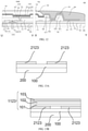
- FIG. 7B illustrates a display panel/an encapsulation structure provided by another embodiment of the present disclosure, which is provided with a first dam 106 to increase the effective length of the stacked-contact portion 1013 as compared with the encapsulation structure illustrated in FIG. 7A .
- the stacked-contact portion 1013 Due to the configuration of edge encapsulation member 104 , the stacked-contact portion 1013 is covered by the edge encapsulation member 104 . Therefore, the first dam 106 can be provided to obtain a stacked-contact portion 1013 with a large effective length. Therefore, even if particles are dropped off, the stacked-contact portion 1013 is not easily ruptured. Thereby, the edge encapsulation member 104 cooperates with the first dam 106 to further improve encapsulation reliability.
- an interval may be provided between the barrier 105 and the encapsulation film 1123 .
- FIG. 8 illustrates a display panel/an encapsulation structure provided by another embodiment of the present disclosure in which no barrier is provided to decrease manufacturing processes.
- a second dam 107 may be provided.
- the second dam 107 is spaced apart from the first dam 106 and formed in the same layer as the first dam 106 .
- the cooperation among the edge encapsulation member 104 , the first dam 106 and the second dam 107 can further improve the encapsulation reliability.
- FIG. 9 illustrates a cross-sectional view taken along lines J-K and M-N in FIG. 6A .
- an edge encapsulation member 104 and a barrier 105 are further provided.
- the barrier 105 may include a plurality of sub-barriers, for example but not limited to a first sub-barrier 1051 , a second sub-barrier 1052 and a third sub-barrier 1053 .
- the first sub-barrier 1051 may be formed in the same layer as the planarization layer 117
- the second sub-barrier 1052 may be formed in the same layer as the pixel definition layer 118
- the third sub-barrier 1053 may be formed in the same layer as a cell thickness support layer (PS).
- PS cell thickness support layer
- the cell thickness support layer is not illustrated in FIG. 9 and may be disposed on the encapsulation film 1123 .
- the edge encapsulation member 104 and the second film 102 have an overlapped part 41 at an edge location in a direction perpendicular to the base substrate 100 .
- the edge encapsulation member 104 and the second thickness encapsulation film 11232 have an overlapped part 41 at the edge location in the direction perpendicular to the base substrate 100 .
- the edge encapsulation member 104 is located at a periphery of the device to be encapsulated 2123 to facilitate edge encapsulation.
- the device to be encapsulated 2123 may include a plurality of devices.
- FIG. 9 illustrates only one device to be encapsulated 2123 .
- the device to be encapsulated 2123 is located within an area defined by an inner edge of the edge encapsulation member 104 in the direction perpendicular to the base substrate 100 , but is not limited thereto.
- the device to be encapsulated 2123 is located within the hollowed-out structure 1040 in the direction perpendicular to the base substrate 100 , but is not limited thereto.
- the encapsulation film 1123 is located on the base substrate 100 and configured to encapsulate the device to be encapsulated on the base substrate 100 .
- FIG. 10 illustrates a schematic view of a mother board/an encapsulation structure of an OLED display panel provided by one or more embodiments of the present disclosure.
- FIG. 10 illustrates two display panels. Single OLED display panels may be formed by way of cutting.
- the OLED display panel may also include the edge encapsulation member 104 .
- FIG. 11 illustrates a cross-sectional view taken along line P-Q in FIG. 10 .
- the display panel/encapsulation structure needs no barrier, which saves process and facilitates leveling while manufacturing the edge encapsulation member 104 .
- edge encapsulation members of adjacent display panels may be separated at the laser cutting process. In this way, there is no need to consider fixed width while printing, thereby increasing edge covering thickness.
- FIG. 12 illustrates a cross-sectional view taken along lines U-V and X-Y in FIG. 10 .
- no barrier 105 is provided.
- an outer edge of the edge encapsulation member 104 is flush with the base substrate 100 .
- the outer edge of the edge encapsulation member 104 may refer to an edge of the edge encapsulation member 104 that is away from the hollowed-out structure 1040 , and for another example, may refer to an edge of a display area or a central area away from the base substrate 100 .
- the edge encapsulation member 104 has a first side FS that is close to the hollowed-out structure 1040 and a second side SS that is away from the hollowed-out 1040 , and an edge of the edge encapsulation member 104 located on the second side SS is flush with the base substrate 100 .
- a process flow for a flexible display product may include the following steps.
- a device to be encapsulated 2123 (OLED devices) are manufactured on the base substrate 100 .
- the device to be encapsulated 2123 may be formed with an evaporation process or an ink jet printing process.
- the base substrate may be a flexible base substrate.
- an OLED device is easily to be eroded by water and oxygen, the erosion is likely to cause failure of the OLED device, therefore, a TFE process is required to form the encapsulation film 1123 .
- An encapsulation film 1123 being a tri-layer film is described as an example. The previous description may be referred to for the first film 101 , the second film 102 and the third film 103 .
- a top protection film (TPF) 131 is attached onto the encapsulation film 1123 with a film attaching process.
- the top protection film 131 needs to cover the entire base substrate 100 .
- the TPF 131 is provided to protect the encapsulation film 1123 in subsequent processes from being damaged. It also functions to keep the base substrate not to drop off the support substrate while separating the base substrate and the support substrate.
- the fourth step as illustrated in FIG. 13D , laser is irradiated on a side of the support substrate 200 away from the base substrate 100 such that the laser is absorbed by the base substrate 100 , the base substrate 100 is carbonized at the contact surface between the support substrate 200 and the base substrate 100 , thereby separating the base substrate 100 and the support substrate 200 .
- a bottom film 141 may be attached on a side of the base substrate 100 away from the device to be encapsulated 2123 for protection.
- the display panel motherboard is cut into small display panels.
- forming 4 display panels will be described as an example.
- a subsequent module process is performed.
- the subsequent module process may include removing the protection film on the display panel and performing subsequent processes.
- the subsequent processes may include film attaching process.
- a step of forming an edge encapsulation member 104 is further included.
- the edge encapsulation member 104 may be formed after forming the encapsulation film 1123 .
- the step of attaching top protection film is performed.
- the encapsulation film 1123 may be formed with an IJP process, a screen printing process or an edge coating process.
- a method for manufacturing a display panel/an encapsulation structure includes: forming a device to be encapsulated 2123 on a base substrate 100 ; forming an encapsulation film 1123 to cover the device to be encapsulated 2123 ; and forming an edge encapsulation member 104 on an edge of the encapsulation film 1123 .
- the edge encapsulation member 104 is in a closed ring structure.
- the edge encapsulation member 104 is made of an organic material.
- the edge encapsulation member 104 and the second film 102 have an overlapped part at the edge location in the direction perpendicular to the base substrate 100 .
- the method may further include forming a barrier 105 .
- the barrier 105 is disposed on a side of the edge encapsulation member 104 away from the encapsulation film 1123 to facilitate manufacturing of the edge encapsulation member 104 .
- an interval is provided between the barrier 105 and the encapsulation film 1123 .
- the barrier 105 may be formed in the same layer as at least one selected from the group consisting of the planarization layer 117 , the pixel definition layer 118 and the cell thickness support layer while manufacturing the OLED display panel so as to reduce manufacturing processes.
- the edge encapsulation member 104 is located at a periphery of the device to be encapsulated 2123 .
- the encapsulation film 1123 includes a first film 101 , a second film 102 and a third film 103 which are sequentially away from the base substrate 100 , the second film 102 is interposed between the first film 101 and the third film 103 .
- the first film 101 is in contact with the third film 103 and the edge encapsulation member 104 covers at least the stacked-contact portion between the first film 101 and the third film 103 .
- the first film 101 and the third film 103 are inorganic films and the second film 102 is an organic film.
- FIG. 15 illustrates a diagram of a method for manufacturing a display panel/an encapsulation structure provided by an embodiment of the present disclosure. As compared with the manufacturing method illustrated in FIGS. 13A-13F , a step of manufacturing the edge encapsulation member is further provided.
- At least one embodiment of the present disclosure provides a light-emitting diode display panel including any of the above-described encapsulation structures.
- the light-emitting diode display panel may be a flexible panel.
- the encapsulation film including three layers of films is described as an example.
- the encapsulation film may further be other structures, for example, may further include more film layers.
- a fourth film and a fifth film may be formed between the base substrate and the first film, the fourth film is closer to the base substrate than the fifth film, and the fourth film may be an inorganic film, and the fifth film may be an organic film.
- the number of films included in the encapsulation film is not limited to what have been described above.
- the encapsulation film may be a structure of alternative organic films and inorganic films.
Landscapes
- Chemical & Material Sciences (AREA)
- Inorganic Chemistry (AREA)
- Engineering & Computer Science (AREA)
- Manufacturing & Machinery (AREA)
- Physics & Mathematics (AREA)
- Optics & Photonics (AREA)
- Microelectronics & Electronic Packaging (AREA)
- Electroluminescent Light Sources (AREA)
- Devices For Indicating Variable Information By Combining Individual Elements (AREA)
Priority Applications (1)
| Application Number | Priority Date | Filing Date | Title |
|---|---|---|---|
| US17/132,208 US11527589B2 (en) | 2017-07-24 | 2020-12-23 | Encapsulation structure, display panel and manufacturing method thereof each having edge encapsulation member on edge of encapsulation film |
Applications Claiming Priority (3)
| Application Number | Priority Date | Filing Date | Title |
|---|---|---|---|
| CN201710607002.0 | 2017-07-24 | ||
| CN201710607002.0A CN109301079B (zh) | 2017-07-24 | 2017-07-24 | 封装结构及其制作方法、发光二极管显示面板 |
| PCT/CN2018/074236 WO2019019580A1 (zh) | 2017-07-24 | 2018-01-26 | 封装结构、显示面板及其制作方法 |
Related Parent Applications (1)
| Application Number | Title | Priority Date | Filing Date |
|---|---|---|---|
| PCT/CN2018/074236 A-371-Of-International WO2019019580A1 (zh) | 2017-07-24 | 2018-01-26 | 封装结构、显示面板及其制作方法 |
Related Child Applications (1)
| Application Number | Title | Priority Date | Filing Date |
|---|---|---|---|
| US17/132,208 Continuation US11527589B2 (en) | 2017-07-24 | 2020-12-23 | Encapsulation structure, display panel and manufacturing method thereof each having edge encapsulation member on edge of encapsulation film |
Publications (2)
| Publication Number | Publication Date |
|---|---|
| US20210175464A1 US20210175464A1 (en) | 2021-06-10 |
| US11233217B2 true US11233217B2 (en) | 2022-01-25 |
Family
ID=65041027
Family Applications (1)
| Application Number | Title | Priority Date | Filing Date |
|---|---|---|---|
| US16/085,421 Active 2039-11-13 US11233217B2 (en) | 2017-07-24 | 2018-01-26 | Encapsulation structure, display panel and manufacturing method thereof each having edge encapsulation member on edge of encapsulation film |
Country Status (6)
| Country | Link |
|---|---|
| US (1) | US11233217B2 (de) |
| EP (1) | EP3660938B1 (de) |
| JP (1) | JP7176954B2 (de) |
| KR (1) | KR102105509B1 (de) |
| CN (1) | CN109301079B (de) |
| WO (1) | WO2019019580A1 (de) |
Cited By (2)
| Publication number | Priority date | Publication date | Assignee | Title |
|---|---|---|---|---|
| US20230180583A1 (en) * | 2019-11-26 | 2023-06-08 | Wuhan China Star Optoelectronics Semiconductor Display Technology Co., Ltd. | Oled display panel |
| US20240251602A1 (en) * | 2022-09-23 | 2024-07-25 | Beijing Boe Technology Development Co., Ltd. | Display Panel and Display Apparatus |
Families Citing this family (11)
| Publication number | Priority date | Publication date | Assignee | Title |
|---|---|---|---|---|
| CN109768184B (zh) * | 2019-02-18 | 2020-10-27 | 武汉华星光电半导体显示技术有限公司 | 一种oled显示面板及其制备方法 |
| JP2020134715A (ja) * | 2019-02-20 | 2020-08-31 | 株式会社ジャパンディスプレイ | 表示装置及び表示装置の製造方法 |
| US11271185B2 (en) * | 2019-02-27 | 2022-03-08 | Wuhan China Star Optoelectronics Semiconductor Display Technology Co., Ltd. | Display structure having a dam and gap |
| CN110148679A (zh) * | 2019-04-29 | 2019-08-20 | 武汉华星光电半导体显示技术有限公司 | 显示面板和电子设备 |
| CN110600631A (zh) * | 2019-08-28 | 2019-12-20 | 武汉华星光电半导体显示技术有限公司 | 显示面板及显示装置 |
| JP7395302B2 (ja) * | 2019-09-30 | 2023-12-11 | 株式会社ジャパンディスプレイ | 表示装置 |
| CN114079021A (zh) * | 2020-08-20 | 2022-02-22 | 上海和辉光电股份有限公司 | 一种低温多晶硅边框和oled屏 |
| KR102945598B1 (ko) * | 2020-12-31 | 2026-03-27 | 엘지디스플레이 주식회사 | 발광 표시 장치와 이를 이용한 멀티 스크린 표시 장치 |
| US20240264449A1 (en) * | 2023-02-02 | 2024-08-08 | Apple Inc. | Systems With Cover Layer Sealing Structures |
| CN116863815B (zh) * | 2023-05-30 | 2025-12-12 | 云谷(固安)科技有限公司 | 显示面板和显示装置 |
| CN118102770B (zh) * | 2024-02-28 | 2024-12-06 | 惠科股份有限公司 | 显示面板、显示面板的制备方法以及显示装置 |
Citations (25)
| Publication number | Priority date | Publication date | Assignee | Title |
|---|---|---|---|---|
| US6081071A (en) * | 1998-05-18 | 2000-06-27 | Motorola, Inc. | Electroluminescent apparatus and methods of manufacturing and encapsulating |
| JP2001228806A (ja) | 2000-02-21 | 2001-08-24 | Toshiba Corp | 平面表示装置 |
| JP2003107519A (ja) | 2001-10-01 | 2003-04-09 | Matsushita Electric Ind Co Ltd | 駆動回路内蔵型tft液晶表示装置及びその製造方法 |
| JP2004103337A (ja) | 2002-09-06 | 2004-04-02 | Semiconductor Energy Lab Co Ltd | 発光装置およびその作製方法 |
| US20040251827A1 (en) * | 2003-06-10 | 2004-12-16 | Kang Tae-Min | Organic electro luminescent display and method for fabricating the same |
| US20070172971A1 (en) * | 2006-01-20 | 2007-07-26 | Eastman Kodak Company | Desiccant sealing arrangement for OLED devices |
| US20110235160A1 (en) | 2010-03-23 | 2011-09-29 | Ming-Che Hsieh | Package structure of a flexible display device |
| US20120287026A1 (en) * | 2010-07-23 | 2012-11-15 | Panasonic Corporation | Display panel and production method thereof |
| JP2013186984A (ja) | 2012-03-07 | 2013-09-19 | Panasonic Corp | 複合基板構造及びその作製方法、並びに、有機エレクトロルミネッセンス素子 |
| JP2014044793A (ja) | 2012-07-31 | 2014-03-13 | Sony Corp | 表示装置および電子機器 |
| US20140131683A1 (en) | 2012-11-09 | 2014-05-15 | Lg Display Co., Ltd. | Flexible organic electroluminescent device and method for fabricating the same |
| US20140183470A1 (en) | 2012-12-28 | 2014-07-03 | Lg Display Co., Ltd. | Organic light emitting diode display device |
| JP2014202934A (ja) | 2013-04-05 | 2014-10-27 | ソニー株式会社 | 表示装置および電子機器 |
| US20150048329A1 (en) | 2013-08-13 | 2015-02-19 | Samsung Display Co., Ltd. | Flexible display |
| US20150221888A1 (en) | 2013-09-10 | 2015-08-06 | Boe Technology Group Co., Ltd. | Encapsulation structure of oled device |
| US20150221892A1 (en) | 2011-12-09 | 2015-08-06 | Samsung Display Co., Ltd. | Organic Light Emitting Diode Display and Method for Manufacturing the Same |
| CN105374946A (zh) | 2015-11-18 | 2016-03-02 | 上海天马微电子有限公司 | 一种柔性显示装置及其制备方法 |
| CN105374947A (zh) | 2015-11-25 | 2016-03-02 | 上海天马有机发光显示技术有限公司 | 有机电致发光器件及其制备方法 |
| US20160190503A1 (en) | 2014-12-30 | 2016-06-30 | Samsung Display Co., Ltd. | Display device |
| CN105914224A (zh) | 2016-05-04 | 2016-08-31 | 京东方科技集团股份有限公司 | 一种有机发光二极管显示基板及其制作方法、显示装置 |
| US20170069873A1 (en) * | 2015-09-07 | 2017-03-09 | Samsung Display Co., Ltd. | Display apparatus |
| CN106601781A (zh) | 2017-01-25 | 2017-04-26 | 上海天马微电子有限公司 | 有机发光显示面板和显示装置 |
| CN106653818A (zh) | 2017-01-23 | 2017-05-10 | 上海天马有机发光显示技术有限公司 | 一种显示面板、显示装置及该显示面板的制备方法 |
| US20170294500A1 (en) * | 2016-04-07 | 2017-10-12 | Samsung Display Co., Ltd. | Display apparatus |
| US20180122890A1 (en) * | 2016-10-31 | 2018-05-03 | Lg Display Co., Ltd. | Organic light emitting display device |
Family Cites Families (2)
| Publication number | Priority date | Publication date | Assignee | Title |
|---|---|---|---|---|
| KR102404577B1 (ko) * | 2015-03-27 | 2022-06-03 | 삼성디스플레이 주식회사 | 유기 발광 표시 장치 |
| KR102477299B1 (ko) * | 2015-06-12 | 2022-12-14 | 삼성디스플레이 주식회사 | 디스플레이 장치 |
-
2017
- 2017-07-24 CN CN201710607002.0A patent/CN109301079B/zh active Active
-
2018
- 2018-01-26 WO PCT/CN2018/074236 patent/WO2019019580A1/zh not_active Ceased
- 2018-01-26 JP JP2018549471A patent/JP7176954B2/ja active Active
- 2018-01-26 KR KR1020187033433A patent/KR102105509B1/ko active Active
- 2018-01-26 EP EP18765791.1A patent/EP3660938B1/de active Active
- 2018-01-26 US US16/085,421 patent/US11233217B2/en active Active
Patent Citations (29)
| Publication number | Priority date | Publication date | Assignee | Title |
|---|---|---|---|---|
| US6081071A (en) * | 1998-05-18 | 2000-06-27 | Motorola, Inc. | Electroluminescent apparatus and methods of manufacturing and encapsulating |
| JP2001228806A (ja) | 2000-02-21 | 2001-08-24 | Toshiba Corp | 平面表示装置 |
| JP2003107519A (ja) | 2001-10-01 | 2003-04-09 | Matsushita Electric Ind Co Ltd | 駆動回路内蔵型tft液晶表示装置及びその製造方法 |
| JP2004103337A (ja) | 2002-09-06 | 2004-04-02 | Semiconductor Energy Lab Co Ltd | 発光装置およびその作製方法 |
| US20040251827A1 (en) * | 2003-06-10 | 2004-12-16 | Kang Tae-Min | Organic electro luminescent display and method for fabricating the same |
| US20070172971A1 (en) * | 2006-01-20 | 2007-07-26 | Eastman Kodak Company | Desiccant sealing arrangement for OLED devices |
| US20110235160A1 (en) | 2010-03-23 | 2011-09-29 | Ming-Che Hsieh | Package structure of a flexible display device |
| US20120287026A1 (en) * | 2010-07-23 | 2012-11-15 | Panasonic Corporation | Display panel and production method thereof |
| US20150221892A1 (en) | 2011-12-09 | 2015-08-06 | Samsung Display Co., Ltd. | Organic Light Emitting Diode Display and Method for Manufacturing the Same |
| JP2013186984A (ja) | 2012-03-07 | 2013-09-19 | Panasonic Corp | 複合基板構造及びその作製方法、並びに、有機エレクトロルミネッセンス素子 |
| US10476031B2 (en) | 2012-07-31 | 2019-11-12 | Joled Inc. | Display unit with moisture proof film outside of seal section and electronic apparatus with said display unit |
| JP2014044793A (ja) | 2012-07-31 | 2014-03-13 | Sony Corp | 表示装置および電子機器 |
| US20140131683A1 (en) | 2012-11-09 | 2014-05-15 | Lg Display Co., Ltd. | Flexible organic electroluminescent device and method for fabricating the same |
| US20140183470A1 (en) | 2012-12-28 | 2014-07-03 | Lg Display Co., Ltd. | Organic light emitting diode display device |
| JP2014202934A (ja) | 2013-04-05 | 2014-10-27 | ソニー株式会社 | 表示装置および電子機器 |
| US9488886B2 (en) | 2013-04-05 | 2016-11-08 | Sony Corporation | Display unit and electronic apparatus |
| KR20150019380A (ko) | 2013-08-13 | 2015-02-25 | 삼성디스플레이 주식회사 | 가요성 표시 장치 |
| US20150048329A1 (en) | 2013-08-13 | 2015-02-19 | Samsung Display Co., Ltd. | Flexible display |
| US20150221888A1 (en) | 2013-09-10 | 2015-08-06 | Boe Technology Group Co., Ltd. | Encapsulation structure of oled device |
| US20160190503A1 (en) | 2014-12-30 | 2016-06-30 | Samsung Display Co., Ltd. | Display device |
| KR20160081106A (ko) | 2014-12-30 | 2016-07-08 | 삼성디스플레이 주식회사 | 표시 장치 |
| US20170069873A1 (en) * | 2015-09-07 | 2017-03-09 | Samsung Display Co., Ltd. | Display apparatus |
| CN105374946A (zh) | 2015-11-18 | 2016-03-02 | 上海天马微电子有限公司 | 一种柔性显示装置及其制备方法 |
| CN105374947A (zh) | 2015-11-25 | 2016-03-02 | 上海天马有机发光显示技术有限公司 | 有机电致发光器件及其制备方法 |
| US20170294500A1 (en) * | 2016-04-07 | 2017-10-12 | Samsung Display Co., Ltd. | Display apparatus |
| CN105914224A (zh) | 2016-05-04 | 2016-08-31 | 京东方科技集团股份有限公司 | 一种有机发光二极管显示基板及其制作方法、显示装置 |
| US20180122890A1 (en) * | 2016-10-31 | 2018-05-03 | Lg Display Co., Ltd. | Organic light emitting display device |
| CN106653818A (zh) | 2017-01-23 | 2017-05-10 | 上海天马有机发光显示技术有限公司 | 一种显示面板、显示装置及该显示面板的制备方法 |
| CN106601781A (zh) | 2017-01-25 | 2017-04-26 | 上海天马微电子有限公司 | 有机发光显示面板和显示装置 |
Non-Patent Citations (7)
| Title |
|---|
| Chinese Office Action in Chinese Application No. 201710607002.0, dated May 21, 2019 with English translation. |
| Extended European Search Report in European Patent Application No. 18765791.1 dated Mar. 9, 2021 in English. |
| International Search Report of PCT/CN2018/074236 in Chinese, dated Apr. 26, 2018, with English translation. |
| Japanese Office Action in Japanese Application No. 2018-549471 dated Nov. 29, 20210 |
| Korean Office Action in Korean Application No. 10-2018-7033433, dated Oct. 30, 2019 with English translation. |
| Notice of Transmittal of the International Search Report of PCT/CN2018/074236 in Chinese, dated Apr. 26, 2018. |
| Written Opinion of the International Searching Authority of PCT/CN2018/074236 in Chinese, dated Apr. 26, 2018, with English translation. |
Cited By (3)
| Publication number | Priority date | Publication date | Assignee | Title |
|---|---|---|---|---|
| US20230180583A1 (en) * | 2019-11-26 | 2023-06-08 | Wuhan China Star Optoelectronics Semiconductor Display Technology Co., Ltd. | Oled display panel |
| US11957029B2 (en) * | 2019-11-26 | 2024-04-09 | Wuhan China Star Optoelectronics Semiconductor Display Technology Co., Ltd. | OLED display panel |
| US20240251602A1 (en) * | 2022-09-23 | 2024-07-25 | Beijing Boe Technology Development Co., Ltd. | Display Panel and Display Apparatus |
Also Published As
| Publication number | Publication date |
|---|---|
| JP2020528156A (ja) | 2020-09-17 |
| CN109301079B (zh) | 2019-10-25 |
| US20210175464A1 (en) | 2021-06-10 |
| KR20190022481A (ko) | 2019-03-06 |
| EP3660938A1 (de) | 2020-06-03 |
| KR102105509B1 (ko) | 2020-04-29 |
| CN109301079A (zh) | 2019-02-01 |
| WO2019019580A1 (zh) | 2019-01-31 |
| JP7176954B2 (ja) | 2022-11-22 |
| EP3660938A4 (de) | 2021-04-07 |
| EP3660938B1 (de) | 2024-03-06 |
Similar Documents
| Publication | Publication Date | Title |
|---|---|---|
| US11233217B2 (en) | Encapsulation structure, display panel and manufacturing method thereof each having edge encapsulation member on edge of encapsulation film | |
| KR102944543B1 (ko) | 유기 발광 디스플레이 장치와, 이의 제조 방법 | |
| US12561017B2 (en) | Touch-control display panel and preparation method therefor, and display apparatus | |
| US10962814B2 (en) | Flexible display device | |
| KR102933722B1 (ko) | 유기발광 표시장치 | |
| KR101763616B1 (ko) | 유기 발광 표시 장치 | |
| CN110246881B (zh) | 柔性显示器 | |
| CN108091675B (zh) | 显示基板及其制作方法 | |
| WO2020211288A1 (zh) | 显示面板及显示装置 | |
| KR102857938B1 (ko) | 플렉서블 유기발광표시장치 | |
| CN113299862B (zh) | 显示面板及其制备方法、显示装置 | |
| US20220320466A1 (en) | Display panel, method for manufacturing same, and display apparatus | |
| US10714704B2 (en) | Foldable display device and method of manufacturing the same | |
| KR102830303B1 (ko) | 유기 발광 표시 장치 및 이의 제조 방법 | |
| US11527589B2 (en) | Encapsulation structure, display panel and manufacturing method thereof each having edge encapsulation member on edge of encapsulation film | |
| CN111971731B (zh) | 显示设备及显示设备的制造方法 | |
| KR20170112416A (ko) | 유기발광 표시장치 및 제조방법 | |
| KR102738864B1 (ko) | 플렉서블 유기발광 표시장치 | |
| CN114400292A (zh) | 显示面板及其制备方法、显示装置 | |
| CN121772508A (zh) | 显示基板及显示装置 |
Legal Events
| Date | Code | Title | Description |
|---|---|---|---|
| AS | Assignment |
Owner name: BOE TECHNOLOGY GROUP CO., LTD., CHINA Free format text: ASSIGNMENT OF ASSIGNORS INTEREST;ASSIGNORS:WANG, WEI;NI, JINGKAI;REEL/FRAME:046881/0329 Effective date: 20180712 |
|
| FEPP | Fee payment procedure |
Free format text: ENTITY STATUS SET TO UNDISCOUNTED (ORIGINAL EVENT CODE: BIG.); ENTITY STATUS OF PATENT OWNER: LARGE ENTITY |
|
| STPP | Information on status: patent application and granting procedure in general |
Free format text: RESPONSE TO NON-FINAL OFFICE ACTION ENTERED AND FORWARDED TO EXAMINER |
|
| STPP | Information on status: patent application and granting procedure in general |
Free format text: NOTICE OF ALLOWANCE MAILED -- APPLICATION RECEIVED IN OFFICE OF PUBLICATIONS |
|
| STPP | Information on status: patent application and granting procedure in general |
Free format text: PUBLICATIONS -- ISSUE FEE PAYMENT VERIFIED |
|
| STCF | Information on status: patent grant |
Free format text: PATENTED CASE |
|
| STPP | Information on status: patent application and granting procedure in general |
Free format text: WITHDRAW FROM ISSUE AWAITING ACTION |
|
| STPP | Information on status: patent application and granting procedure in general |
Free format text: AWAITING TC RESP., ISSUE FEE NOT PAID |
|
| STPP | Information on status: patent application and granting procedure in general |
Free format text: PUBLICATIONS -- ISSUE FEE PAYMENT VERIFIED |
|
| STCF | Information on status: patent grant |
Free format text: PATENTED CASE |
|
| MAFP | Maintenance fee payment |
Free format text: PAYMENT OF MAINTENANCE FEE, 4TH YEAR, LARGE ENTITY (ORIGINAL EVENT CODE: M1551); ENTITY STATUS OF PATENT OWNER: LARGE ENTITY Year of fee payment: 4 |