US10867964B2 - Semiconductor assemblies using edge stacking and methods of manufacturing the same - Google Patents
Semiconductor assemblies using edge stacking and methods of manufacturing the same Download PDFInfo
- Publication number
- US10867964B2 US10867964B2 US16/510,929 US201916510929A US10867964B2 US 10867964 B2 US10867964 B2 US 10867964B2 US 201916510929 A US201916510929 A US 201916510929A US 10867964 B2 US10867964 B2 US 10867964B2
- Authority
- US
- United States
- Prior art keywords
- substrate
- base
- semiconductor
- die
- outermost
- Prior art date
- Legal status (The legal status is an assumption and is not a legal conclusion. Google has not performed a legal analysis and makes no representation as to the accuracy of the status listed.)
- Active
Links
Images


Classifications
-
- H—ELECTRICITY
- H01—ELECTRIC ELEMENTS
- H01L—SEMICONDUCTOR DEVICES NOT COVERED BY CLASS H10
- H01L23/00—Details of semiconductor or other solid state devices
- H01L23/02—Containers; Seals
- H01L23/04—Containers; Seals characterised by the shape of the container or parts, e.g. caps, walls
- H01L23/053—Containers; Seals characterised by the shape of the container or parts, e.g. caps, walls the container being a hollow construction and having an insulating or insulated base as a mounting for the semiconductor body
-
- H—ELECTRICITY
- H01—ELECTRIC ELEMENTS
- H01L—SEMICONDUCTOR DEVICES NOT COVERED BY CLASS H10
- H01L25/00—Assemblies consisting of a plurality of individual semiconductor or other solid state devices ; Multistep manufacturing processes thereof
- H01L25/03—Assemblies consisting of a plurality of individual semiconductor or other solid state devices ; Multistep manufacturing processes thereof all the devices being of a type provided for in the same subgroup of groups H01L27/00 - H01L33/00, or in a single subclass of H10K, H10N, e.g. assemblies of rectifier diodes
- H01L25/04—Assemblies consisting of a plurality of individual semiconductor or other solid state devices ; Multistep manufacturing processes thereof all the devices being of a type provided for in the same subgroup of groups H01L27/00 - H01L33/00, or in a single subclass of H10K, H10N, e.g. assemblies of rectifier diodes the devices not having separate containers
- H01L25/065—Assemblies consisting of a plurality of individual semiconductor or other solid state devices ; Multistep manufacturing processes thereof all the devices being of a type provided for in the same subgroup of groups H01L27/00 - H01L33/00, or in a single subclass of H10K, H10N, e.g. assemblies of rectifier diodes the devices not having separate containers the devices being of a type provided for in group H01L27/00
- H01L25/0652—Assemblies consisting of a plurality of individual semiconductor or other solid state devices ; Multistep manufacturing processes thereof all the devices being of a type provided for in the same subgroup of groups H01L27/00 - H01L33/00, or in a single subclass of H10K, H10N, e.g. assemblies of rectifier diodes the devices not having separate containers the devices being of a type provided for in group H01L27/00 the devices being arranged next and on each other, i.e. mixed assemblies
-
- H—ELECTRICITY
- H01—ELECTRIC ELEMENTS
- H01L—SEMICONDUCTOR DEVICES NOT COVERED BY CLASS H10
- H01L23/00—Details of semiconductor or other solid state devices
- H01L23/16—Fillings or auxiliary members in containers or encapsulations, e.g. centering rings
- H01L23/18—Fillings characterised by the material, its physical or chemical properties, or its arrangement within the complete device
- H01L23/24—Fillings characterised by the material, its physical or chemical properties, or its arrangement within the complete device solid or gel at the normal operating temperature of the device
-
- H—ELECTRICITY
- H01—ELECTRIC ELEMENTS
- H01L—SEMICONDUCTOR DEVICES NOT COVERED BY CLASS H10
- H01L23/00—Details of semiconductor or other solid state devices
- H01L23/28—Encapsulations, e.g. encapsulating layers, coatings, e.g. for protection
- H01L23/31—Encapsulations, e.g. encapsulating layers, coatings, e.g. for protection characterised by the arrangement or shape
- H01L23/3107—Encapsulations, e.g. encapsulating layers, coatings, e.g. for protection characterised by the arrangement or shape the device being completely enclosed
- H01L23/3121—Encapsulations, e.g. encapsulating layers, coatings, e.g. for protection characterised by the arrangement or shape the device being completely enclosed a substrate forming part of the encapsulation
- H01L23/3128—Encapsulations, e.g. encapsulating layers, coatings, e.g. for protection characterised by the arrangement or shape the device being completely enclosed a substrate forming part of the encapsulation the substrate having spherical bumps for external connection
-
- H—ELECTRICITY
- H01—ELECTRIC ELEMENTS
- H01L—SEMICONDUCTOR DEVICES NOT COVERED BY CLASS H10
- H01L23/00—Details of semiconductor or other solid state devices
- H01L23/48—Arrangements for conducting electric current to or from the solid state body in operation, e.g. leads, terminal arrangements ; Selection of materials therefor
- H01L23/488—Arrangements for conducting electric current to or from the solid state body in operation, e.g. leads, terminal arrangements ; Selection of materials therefor consisting of soldered or bonded constructions
- H01L23/498—Leads, i.e. metallisations or lead-frames on insulating substrates, e.g. chip carriers
- H01L23/49811—Additional leads joined to the metallisation on the insulating substrate, e.g. pins, bumps, wires, flat leads
- H01L23/49816—Spherical bumps on the substrate for external connection, e.g. ball grid arrays [BGA]
-
- H—ELECTRICITY
- H01—ELECTRIC ELEMENTS
- H01L—SEMICONDUCTOR DEVICES NOT COVERED BY CLASS H10
- H01L23/00—Details of semiconductor or other solid state devices
- H01L23/52—Arrangements for conducting electric current within the device in operation from one component to another, i.e. interconnections, e.g. wires, lead frames
- H01L23/522—Arrangements for conducting electric current within the device in operation from one component to another, i.e. interconnections, e.g. wires, lead frames including external interconnections consisting of a multilayer structure of conductive and insulating layers inseparably formed on the semiconductor body
- H01L23/5226—Via connections in a multilevel interconnection structure
-
- H—ELECTRICITY
- H01—ELECTRIC ELEMENTS
- H01L—SEMICONDUCTOR DEVICES NOT COVERED BY CLASS H10
- H01L24/00—Arrangements for connecting or disconnecting semiconductor or solid-state bodies; Methods or apparatus related thereto
- H01L24/01—Means for bonding being attached to, or being formed on, the surface to be connected, e.g. chip-to-package, die-attach, "first-level" interconnects; Manufacturing methods related thereto
- H01L24/10—Bump connectors ; Manufacturing methods related thereto
- H01L24/12—Structure, shape, material or disposition of the bump connectors prior to the connecting process
- H01L24/13—Structure, shape, material or disposition of the bump connectors prior to the connecting process of an individual bump connector
-
- H—ELECTRICITY
- H01—ELECTRIC ELEMENTS
- H01L—SEMICONDUCTOR DEVICES NOT COVERED BY CLASS H10
- H01L24/00—Arrangements for connecting or disconnecting semiconductor or solid-state bodies; Methods or apparatus related thereto
- H01L24/01—Means for bonding being attached to, or being formed on, the surface to be connected, e.g. chip-to-package, die-attach, "first-level" interconnects; Manufacturing methods related thereto
- H01L24/10—Bump connectors ; Manufacturing methods related thereto
- H01L24/12—Structure, shape, material or disposition of the bump connectors prior to the connecting process
- H01L24/14—Structure, shape, material or disposition of the bump connectors prior to the connecting process of a plurality of bump connectors
-
- H—ELECTRICITY
- H01—ELECTRIC ELEMENTS
- H01L—SEMICONDUCTOR DEVICES NOT COVERED BY CLASS H10
- H01L24/00—Arrangements for connecting or disconnecting semiconductor or solid-state bodies; Methods or apparatus related thereto
- H01L24/01—Means for bonding being attached to, or being formed on, the surface to be connected, e.g. chip-to-package, die-attach, "first-level" interconnects; Manufacturing methods related thereto
- H01L24/10—Bump connectors ; Manufacturing methods related thereto
- H01L24/15—Structure, shape, material or disposition of the bump connectors after the connecting process
- H01L24/16—Structure, shape, material or disposition of the bump connectors after the connecting process of an individual bump connector
-
- H—ELECTRICITY
- H01—ELECTRIC ELEMENTS
- H01L—SEMICONDUCTOR DEVICES NOT COVERED BY CLASS H10
- H01L24/00—Arrangements for connecting or disconnecting semiconductor or solid-state bodies; Methods or apparatus related thereto
- H01L24/01—Means for bonding being attached to, or being formed on, the surface to be connected, e.g. chip-to-package, die-attach, "first-level" interconnects; Manufacturing methods related thereto
- H01L24/10—Bump connectors ; Manufacturing methods related thereto
- H01L24/15—Structure, shape, material or disposition of the bump connectors after the connecting process
- H01L24/17—Structure, shape, material or disposition of the bump connectors after the connecting process of a plurality of bump connectors
-
- H—ELECTRICITY
- H01—ELECTRIC ELEMENTS
- H01L—SEMICONDUCTOR DEVICES NOT COVERED BY CLASS H10
- H01L24/00—Arrangements for connecting or disconnecting semiconductor or solid-state bodies; Methods or apparatus related thereto
- H01L24/01—Means for bonding being attached to, or being formed on, the surface to be connected, e.g. chip-to-package, die-attach, "first-level" interconnects; Manufacturing methods related thereto
- H01L24/42—Wire connectors; Manufacturing methods related thereto
- H01L24/43—Manufacturing methods
-
- H—ELECTRICITY
- H01—ELECTRIC ELEMENTS
- H01L—SEMICONDUCTOR DEVICES NOT COVERED BY CLASS H10
- H01L24/00—Arrangements for connecting or disconnecting semiconductor or solid-state bodies; Methods or apparatus related thereto
- H01L24/01—Means for bonding being attached to, or being formed on, the surface to be connected, e.g. chip-to-package, die-attach, "first-level" interconnects; Manufacturing methods related thereto
- H01L24/42—Wire connectors; Manufacturing methods related thereto
- H01L24/47—Structure, shape, material or disposition of the wire connectors after the connecting process
- H01L24/48—Structure, shape, material or disposition of the wire connectors after the connecting process of an individual wire connector
-
- H—ELECTRICITY
- H01—ELECTRIC ELEMENTS
- H01L—SEMICONDUCTOR DEVICES NOT COVERED BY CLASS H10
- H01L24/00—Arrangements for connecting or disconnecting semiconductor or solid-state bodies; Methods or apparatus related thereto
- H01L24/01—Means for bonding being attached to, or being formed on, the surface to be connected, e.g. chip-to-package, die-attach, "first-level" interconnects; Manufacturing methods related thereto
- H01L24/42—Wire connectors; Manufacturing methods related thereto
- H01L24/47—Structure, shape, material or disposition of the wire connectors after the connecting process
- H01L24/49—Structure, shape, material or disposition of the wire connectors after the connecting process of a plurality of wire connectors
-
- H—ELECTRICITY
- H01—ELECTRIC ELEMENTS
- H01L—SEMICONDUCTOR DEVICES NOT COVERED BY CLASS H10
- H01L24/00—Arrangements for connecting or disconnecting semiconductor or solid-state bodies; Methods or apparatus related thereto
- H01L24/01—Means for bonding being attached to, or being formed on, the surface to be connected, e.g. chip-to-package, die-attach, "first-level" interconnects; Manufacturing methods related thereto
- H01L24/63—Connectors not provided for in any of the groups H01L24/10 - H01L24/50 and subgroups; Manufacturing methods related thereto
- H01L24/65—Structure, shape, material or disposition of the connectors prior to the connecting process
- H01L24/66—Structure, shape, material or disposition of the connectors prior to the connecting process of an individual connector
-
- H—ELECTRICITY
- H01—ELECTRIC ELEMENTS
- H01L—SEMICONDUCTOR DEVICES NOT COVERED BY CLASS H10
- H01L24/00—Arrangements for connecting or disconnecting semiconductor or solid-state bodies; Methods or apparatus related thereto
- H01L24/01—Means for bonding being attached to, or being formed on, the surface to be connected, e.g. chip-to-package, die-attach, "first-level" interconnects; Manufacturing methods related thereto
- H01L24/63—Connectors not provided for in any of the groups H01L24/10 - H01L24/50 and subgroups; Manufacturing methods related thereto
- H01L24/65—Structure, shape, material or disposition of the connectors prior to the connecting process
- H01L24/67—Structure, shape, material or disposition of the connectors prior to the connecting process of a plurality of connectors
-
- H—ELECTRICITY
- H01—ELECTRIC ELEMENTS
- H01L—SEMICONDUCTOR DEVICES NOT COVERED BY CLASS H10
- H01L24/00—Arrangements for connecting or disconnecting semiconductor or solid-state bodies; Methods or apparatus related thereto
- H01L24/73—Means for bonding being of different types provided for in two or more of groups H01L24/10, H01L24/18, H01L24/26, H01L24/34, H01L24/42, H01L24/50, H01L24/63, H01L24/71
-
- H—ELECTRICITY
- H01—ELECTRIC ELEMENTS
- H01L—SEMICONDUCTOR DEVICES NOT COVERED BY CLASS H10
- H01L25/00—Assemblies consisting of a plurality of individual semiconductor or other solid state devices ; Multistep manufacturing processes thereof
- H01L25/03—Assemblies consisting of a plurality of individual semiconductor or other solid state devices ; Multistep manufacturing processes thereof all the devices being of a type provided for in the same subgroup of groups H01L27/00 - H01L33/00, or in a single subclass of H10K, H10N, e.g. assemblies of rectifier diodes
- H01L25/04—Assemblies consisting of a plurality of individual semiconductor or other solid state devices ; Multistep manufacturing processes thereof all the devices being of a type provided for in the same subgroup of groups H01L27/00 - H01L33/00, or in a single subclass of H10K, H10N, e.g. assemblies of rectifier diodes the devices not having separate containers
- H01L25/065—Assemblies consisting of a plurality of individual semiconductor or other solid state devices ; Multistep manufacturing processes thereof all the devices being of a type provided for in the same subgroup of groups H01L27/00 - H01L33/00, or in a single subclass of H10K, H10N, e.g. assemblies of rectifier diodes the devices not having separate containers the devices being of a type provided for in group H01L27/00
- H01L25/0657—Stacked arrangements of devices
-
- H—ELECTRICITY
- H01—ELECTRIC ELEMENTS
- H01L—SEMICONDUCTOR DEVICES NOT COVERED BY CLASS H10
- H01L2224/00—Indexing scheme for arrangements for connecting or disconnecting semiconductor or solid-state bodies and methods related thereto as covered by H01L24/00
- H01L2224/01—Means for bonding being attached to, or being formed on, the surface to be connected, e.g. chip-to-package, die-attach, "first-level" interconnects; Manufacturing methods related thereto
- H01L2224/10—Bump connectors; Manufacturing methods related thereto
- H01L2224/12—Structure, shape, material or disposition of the bump connectors prior to the connecting process
- H01L2224/13—Structure, shape, material or disposition of the bump connectors prior to the connecting process of an individual bump connector
- H01L2224/13001—Core members of the bump connector
- H01L2224/13099—Material
-
- H—ELECTRICITY
- H01—ELECTRIC ELEMENTS
- H01L—SEMICONDUCTOR DEVICES NOT COVERED BY CLASS H10
- H01L2224/00—Indexing scheme for arrangements for connecting or disconnecting semiconductor or solid-state bodies and methods related thereto as covered by H01L24/00
- H01L2224/01—Means for bonding being attached to, or being formed on, the surface to be connected, e.g. chip-to-package, die-attach, "first-level" interconnects; Manufacturing methods related thereto
- H01L2224/10—Bump connectors; Manufacturing methods related thereto
- H01L2224/12—Structure, shape, material or disposition of the bump connectors prior to the connecting process
- H01L2224/14—Structure, shape, material or disposition of the bump connectors prior to the connecting process of a plurality of bump connectors
- H01L2224/141—Disposition
- H01L2224/14104—Disposition relative to the bonding areas, e.g. bond pads, of the semiconductor or solid-state body
- H01L2224/1411—Disposition relative to the bonding areas, e.g. bond pads, of the semiconductor or solid-state body the bump connectors being bonded to at least one common bonding area
-
- H—ELECTRICITY
- H01—ELECTRIC ELEMENTS
- H01L—SEMICONDUCTOR DEVICES NOT COVERED BY CLASS H10
- H01L2224/00—Indexing scheme for arrangements for connecting or disconnecting semiconductor or solid-state bodies and methods related thereto as covered by H01L24/00
- H01L2224/01—Means for bonding being attached to, or being formed on, the surface to be connected, e.g. chip-to-package, die-attach, "first-level" interconnects; Manufacturing methods related thereto
- H01L2224/10—Bump connectors; Manufacturing methods related thereto
- H01L2224/12—Structure, shape, material or disposition of the bump connectors prior to the connecting process
- H01L2224/14—Structure, shape, material or disposition of the bump connectors prior to the connecting process of a plurality of bump connectors
- H01L2224/141—Disposition
- H01L2224/1418—Disposition being disposed on at least two different sides of the body, e.g. dual array
- H01L2224/14181—On opposite sides of the body
-
- H—ELECTRICITY
- H01—ELECTRIC ELEMENTS
- H01L—SEMICONDUCTOR DEVICES NOT COVERED BY CLASS H10
- H01L2224/00—Indexing scheme for arrangements for connecting or disconnecting semiconductor or solid-state bodies and methods related thereto as covered by H01L24/00
- H01L2224/01—Means for bonding being attached to, or being formed on, the surface to be connected, e.g. chip-to-package, die-attach, "first-level" interconnects; Manufacturing methods related thereto
- H01L2224/10—Bump connectors; Manufacturing methods related thereto
- H01L2224/15—Structure, shape, material or disposition of the bump connectors after the connecting process
- H01L2224/16—Structure, shape, material or disposition of the bump connectors after the connecting process of an individual bump connector
- H01L2224/161—Disposition
- H01L2224/16135—Disposition the bump connector connecting between different semiconductor or solid-state bodies, i.e. chip-to-chip
- H01L2224/16145—Disposition the bump connector connecting between different semiconductor or solid-state bodies, i.e. chip-to-chip the bodies being stacked
-
- H—ELECTRICITY
- H01—ELECTRIC ELEMENTS
- H01L—SEMICONDUCTOR DEVICES NOT COVERED BY CLASS H10
- H01L2224/00—Indexing scheme for arrangements for connecting or disconnecting semiconductor or solid-state bodies and methods related thereto as covered by H01L24/00
- H01L2224/01—Means for bonding being attached to, or being formed on, the surface to be connected, e.g. chip-to-package, die-attach, "first-level" interconnects; Manufacturing methods related thereto
- H01L2224/10—Bump connectors; Manufacturing methods related thereto
- H01L2224/15—Structure, shape, material or disposition of the bump connectors after the connecting process
- H01L2224/16—Structure, shape, material or disposition of the bump connectors after the connecting process of an individual bump connector
- H01L2224/161—Disposition
- H01L2224/16151—Disposition the bump connector connecting between a semiconductor or solid-state body and an item not being a semiconductor or solid-state body, e.g. chip-to-substrate, chip-to-passive
- H01L2224/16221—Disposition the bump connector connecting between a semiconductor or solid-state body and an item not being a semiconductor or solid-state body, e.g. chip-to-substrate, chip-to-passive the body and the item being stacked
- H01L2224/16225—Disposition the bump connector connecting between a semiconductor or solid-state body and an item not being a semiconductor or solid-state body, e.g. chip-to-substrate, chip-to-passive the body and the item being stacked the item being non-metallic, e.g. insulating substrate with or without metallisation
-
- H—ELECTRICITY
- H01—ELECTRIC ELEMENTS
- H01L—SEMICONDUCTOR DEVICES NOT COVERED BY CLASS H10
- H01L2224/00—Indexing scheme for arrangements for connecting or disconnecting semiconductor or solid-state bodies and methods related thereto as covered by H01L24/00
- H01L2224/01—Means for bonding being attached to, or being formed on, the surface to be connected, e.g. chip-to-package, die-attach, "first-level" interconnects; Manufacturing methods related thereto
- H01L2224/26—Layer connectors, e.g. plate connectors, solder or adhesive layers; Manufacturing methods related thereto
- H01L2224/28—Structure, shape, material or disposition of the layer connectors prior to the connecting process
- H01L2224/29—Structure, shape, material or disposition of the layer connectors prior to the connecting process of an individual layer connector
- H01L2224/29001—Core members of the layer connector
- H01L2224/29099—Material
-
- H—ELECTRICITY
- H01—ELECTRIC ELEMENTS
- H01L—SEMICONDUCTOR DEVICES NOT COVERED BY CLASS H10
- H01L2224/00—Indexing scheme for arrangements for connecting or disconnecting semiconductor or solid-state bodies and methods related thereto as covered by H01L24/00
- H01L2224/01—Means for bonding being attached to, or being formed on, the surface to be connected, e.g. chip-to-package, die-attach, "first-level" interconnects; Manufacturing methods related thereto
- H01L2224/26—Layer connectors, e.g. plate connectors, solder or adhesive layers; Manufacturing methods related thereto
- H01L2224/31—Structure, shape, material or disposition of the layer connectors after the connecting process
- H01L2224/32—Structure, shape, material or disposition of the layer connectors after the connecting process of an individual layer connector
- H01L2224/321—Disposition
- H01L2224/32151—Disposition the layer connector connecting between a semiconductor or solid-state body and an item not being a semiconductor or solid-state body, e.g. chip-to-substrate, chip-to-passive
- H01L2224/32221—Disposition the layer connector connecting between a semiconductor or solid-state body and an item not being a semiconductor or solid-state body, e.g. chip-to-substrate, chip-to-passive the body and the item being stacked
- H01L2224/32225—Disposition the layer connector connecting between a semiconductor or solid-state body and an item not being a semiconductor or solid-state body, e.g. chip-to-substrate, chip-to-passive the body and the item being stacked the item being non-metallic, e.g. insulating substrate with or without metallisation
-
- H—ELECTRICITY
- H01—ELECTRIC ELEMENTS
- H01L—SEMICONDUCTOR DEVICES NOT COVERED BY CLASS H10
- H01L2224/00—Indexing scheme for arrangements for connecting or disconnecting semiconductor or solid-state bodies and methods related thereto as covered by H01L24/00
- H01L2224/01—Means for bonding being attached to, or being formed on, the surface to be connected, e.g. chip-to-package, die-attach, "first-level" interconnects; Manufacturing methods related thereto
- H01L2224/42—Wire connectors; Manufacturing methods related thereto
- H01L2224/44—Structure, shape, material or disposition of the wire connectors prior to the connecting process
- H01L2224/45—Structure, shape, material or disposition of the wire connectors prior to the connecting process of an individual wire connector
- H01L2224/45001—Core members of the connector
- H01L2224/45099—Material
-
- H—ELECTRICITY
- H01—ELECTRIC ELEMENTS
- H01L—SEMICONDUCTOR DEVICES NOT COVERED BY CLASS H10
- H01L2224/00—Indexing scheme for arrangements for connecting or disconnecting semiconductor or solid-state bodies and methods related thereto as covered by H01L24/00
- H01L2224/73—Means for bonding being of different types provided for in two or more of groups H01L2224/10, H01L2224/18, H01L2224/26, H01L2224/34, H01L2224/42, H01L2224/50, H01L2224/63, H01L2224/71
- H01L2224/732—Location after the connecting process
- H01L2224/73251—Location after the connecting process on different surfaces
- H01L2224/73253—Bump and layer connectors
-
- H—ELECTRICITY
- H01—ELECTRIC ELEMENTS
- H01L—SEMICONDUCTOR DEVICES NOT COVERED BY CLASS H10
- H01L2224/00—Indexing scheme for arrangements for connecting or disconnecting semiconductor or solid-state bodies and methods related thereto as covered by H01L24/00
- H01L2224/73—Means for bonding being of different types provided for in two or more of groups H01L2224/10, H01L2224/18, H01L2224/26, H01L2224/34, H01L2224/42, H01L2224/50, H01L2224/63, H01L2224/71
- H01L2224/732—Location after the connecting process
- H01L2224/73251—Location after the connecting process on different surfaces
- H01L2224/73257—Bump and wire connectors
-
- H—ELECTRICITY
- H01—ELECTRIC ELEMENTS
- H01L—SEMICONDUCTOR DEVICES NOT COVERED BY CLASS H10
- H01L2225/00—Details relating to assemblies covered by the group H01L25/00 but not provided for in its subgroups
- H01L2225/03—All the devices being of a type provided for in the same subgroup of groups H01L27/00 - H01L33/648 and H10K99/00
- H01L2225/04—All the devices being of a type provided for in the same subgroup of groups H01L27/00 - H01L33/648 and H10K99/00 the devices not having separate containers
- H01L2225/065—All the devices being of a type provided for in the same subgroup of groups H01L27/00 - H01L33/648 and H10K99/00 the devices not having separate containers the devices being of a type provided for in group H01L27/00
- H01L2225/06503—Stacked arrangements of devices
- H01L2225/06513—Bump or bump-like direct electrical connections between devices, e.g. flip-chip connection, solder bumps
-
- H—ELECTRICITY
- H01—ELECTRIC ELEMENTS
- H01L—SEMICONDUCTOR DEVICES NOT COVERED BY CLASS H10
- H01L2225/00—Details relating to assemblies covered by the group H01L25/00 but not provided for in its subgroups
- H01L2225/03—All the devices being of a type provided for in the same subgroup of groups H01L27/00 - H01L33/648 and H10K99/00
- H01L2225/04—All the devices being of a type provided for in the same subgroup of groups H01L27/00 - H01L33/648 and H10K99/00 the devices not having separate containers
- H01L2225/065—All the devices being of a type provided for in the same subgroup of groups H01L27/00 - H01L33/648 and H10K99/00 the devices not having separate containers the devices being of a type provided for in group H01L27/00
- H01L2225/06503—Stacked arrangements of devices
- H01L2225/06524—Electrical connections formed on device or on substrate, e.g. a deposited or grown layer
-
- H—ELECTRICITY
- H01—ELECTRIC ELEMENTS
- H01L—SEMICONDUCTOR DEVICES NOT COVERED BY CLASS H10
- H01L2225/00—Details relating to assemblies covered by the group H01L25/00 but not provided for in its subgroups
- H01L2225/03—All the devices being of a type provided for in the same subgroup of groups H01L27/00 - H01L33/648 and H10K99/00
- H01L2225/04—All the devices being of a type provided for in the same subgroup of groups H01L27/00 - H01L33/648 and H10K99/00 the devices not having separate containers
- H01L2225/065—All the devices being of a type provided for in the same subgroup of groups H01L27/00 - H01L33/648 and H10K99/00 the devices not having separate containers the devices being of a type provided for in group H01L27/00
- H01L2225/06503—Stacked arrangements of devices
- H01L2225/06527—Special adaptation of electrical connections, e.g. rewiring, engineering changes, pressure contacts, layout
-
- H—ELECTRICITY
- H01—ELECTRIC ELEMENTS
- H01L—SEMICONDUCTOR DEVICES NOT COVERED BY CLASS H10
- H01L2225/00—Details relating to assemblies covered by the group H01L25/00 but not provided for in its subgroups
- H01L2225/03—All the devices being of a type provided for in the same subgroup of groups H01L27/00 - H01L33/648 and H10K99/00
- H01L2225/04—All the devices being of a type provided for in the same subgroup of groups H01L27/00 - H01L33/648 and H10K99/00 the devices not having separate containers
- H01L2225/065—All the devices being of a type provided for in the same subgroup of groups H01L27/00 - H01L33/648 and H10K99/00 the devices not having separate containers the devices being of a type provided for in group H01L27/00
- H01L2225/06503—Stacked arrangements of devices
- H01L2225/06582—Housing for the assembly, e.g. chip scale package [CSP]
-
- H—ELECTRICITY
- H01—ELECTRIC ELEMENTS
- H01L—SEMICONDUCTOR DEVICES NOT COVERED BY CLASS H10
- H01L24/00—Arrangements for connecting or disconnecting semiconductor or solid-state bodies; Methods or apparatus related thereto
- H01L24/01—Means for bonding being attached to, or being formed on, the surface to be connected, e.g. chip-to-package, die-attach, "first-level" interconnects; Manufacturing methods related thereto
- H01L24/26—Layer connectors, e.g. plate connectors, solder or adhesive layers; Manufacturing methods related thereto
- H01L24/31—Structure, shape, material or disposition of the layer connectors after the connecting process
- H01L24/32—Structure, shape, material or disposition of the layer connectors after the connecting process of an individual layer connector
-
- H—ELECTRICITY
- H01—ELECTRIC ELEMENTS
- H01L—SEMICONDUCTOR DEVICES NOT COVERED BY CLASS H10
- H01L2924/00—Indexing scheme for arrangements or methods for connecting or disconnecting semiconductor or solid-state bodies as covered by H01L24/00
- H01L2924/0001—Technical content checked by a classifier
- H01L2924/00012—Relevant to the scope of the group, the symbol of which is combined with the symbol of this group
-
- H—ELECTRICITY
- H01—ELECTRIC ELEMENTS
- H01L—SEMICONDUCTOR DEVICES NOT COVERED BY CLASS H10
- H01L2924/00—Indexing scheme for arrangements or methods for connecting or disconnecting semiconductor or solid-state bodies as covered by H01L24/00
- H01L2924/0001—Technical content checked by a classifier
- H01L2924/00014—Technical content checked by a classifier the subject-matter covered by the group, the symbol of which is combined with the symbol of this group, being disclosed without further technical details
-
- H—ELECTRICITY
- H01—ELECTRIC ELEMENTS
- H01L—SEMICONDUCTOR DEVICES NOT COVERED BY CLASS H10
- H01L2924/00—Indexing scheme for arrangements or methods for connecting or disconnecting semiconductor or solid-state bodies as covered by H01L24/00
- H01L2924/15—Details of package parts other than the semiconductor or other solid state devices to be connected
- H01L2924/181—Encapsulation
-
- H—ELECTRICITY
- H01—ELECTRIC ELEMENTS
- H01L—SEMICONDUCTOR DEVICES NOT COVERED BY CLASS H10
- H01L2924/00—Indexing scheme for arrangements or methods for connecting or disconnecting semiconductor or solid-state bodies as covered by H01L24/00
- H01L2924/19—Details of hybrid assemblies other than the semiconductor or other solid state devices to be connected
- H01L2924/191—Disposition
- H01L2924/19101—Disposition of discrete passive components
- H01L2924/19107—Disposition of discrete passive components off-chip wires
Definitions
- the present technology is directed to packaging semiconductor devices, such as memory and processors, and several embodiments are directed to semiconductor assemblies that use modular edge stacking.
- Packaged semiconductor dies typically include a semiconductor die mounted on a substrate and encased in a plastic protective covering.
- the die includes functional features, such as memory cells, processor circuits, and interconnecting circuitry, as well as bond pads electrically connected to the functional features.
- the bond pads are often electrically connected to external terminals that extend outside of the protective covering to allow the die to be connected to busses, circuits or other higher level circuitry.
- Semiconductor die manufacturers are under increasing pressure to continually reduce the size of die packages to fit within the space constraints of electronic devices, while also increasing the functional capacity of each package to meet operating parameters.
- One approach for increasing the processing power of a semiconductor package without substantially increasing the surface area covered by the package i.e., the package's “footprint”
- the package's “footprint” is to vertically stack multiple semiconductor dies on top of one another in a single package. Stacking multiple dies, however, increases the vertical profile of the device, requiring the individual dies to be thinned substantially to achieve a vertically compact size. Additionally, the stacking of multiple dies can increase the probability of device failure, and lead to higher costs associated with longer manufacturing and testing times.
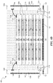
- FIG. 1 illustrates a conventional system 10 including multiple semiconductor stacked assemblies.
- the system 10 includes printed circuit boards (PCBs) 15 arranged in dual in-line memory module (DIMM) slots and separated from one another by a given center-line to center-line pitch (i.e., ⁇ 7.6 mm).
- Semiconductor packages 12 are attached to each of the PCBs 15 in a stacked arrangement. Specifically, bottom portions of each semiconductor package 12 are attached via solder balls 13 to opposite sides of the PCBs 15 .
- the conventional system 10 has limited space between the semiconductor packages 12 (i.e, ⁇ 1 mm) on adjacent DIMM slots, which can limit airflow therebetween required for thermal control and restrict the performance of the packages. Accordingly, there is a need for other approaches to provide semiconductor devices with smaller footprints, while still maintaining sufficient functional capacity to meet operating parameters.
- FIG. 1 is a schematic side view of a semiconductor device assembly in accordance with the prior art.
- FIG. 2A is a schematic top view of a semiconductor device package taken along line 2 A- 2 A of FIG. 2B , and configured in accordance with embodiments of the present technology.
- FIG. 2B is a schematic cross-sectional view of the semiconductor device package shown in FIG. 2A taken along line 2 B- 2 B of FIG. 2A , and configured in accordance with embodiments of the present technology.
- FIG. 3A is a schematic top view of a semiconductor device package taken along line 3 A- 3 A of FIG. 3B , and configured in accordance with embodiments of the present technology.
- FIG. 3B is a schematic cross-sectional view of the semiconductor device package shown in FIG. 3A taken along line 3 B- 3 B of FIG. 3A , and configured in accordance with embodiments of the present technology.
- FIGS. 4A-4D are schematic views illustrating a method of forming a semiconductor device package configured in accordance with embodiments of the present technology.
- FIG. 5 is a schematic cross-sectional view of a semiconductor device package configured in accordance with embodiments of the present technology.
- FIGS. 6A-6C and 7A-7D are schematic views of semiconductor device assemblies configured in accordance with embodiments of the present technology.
- FIG. 8 is a schematic view of a system that includes a semiconductor assembly configured in accordance with embodiments of the present technology.
- each semiconductor package comprises a first substrate having a first surface, a second substrate having a second surface orthogonal to the first surface, and one or more dies disposed over the first surface of the first substrate.
- the semiconductor package further comprises one or more interconnections extending from the second surface of the second substrate to at least one of (a) the first surface of the first substrate, or (b) an outermost surface of the one or more dies.
- the semiconductor packages can be electrically coupled to neighboring semiconductor packages via external connection sites at outer surfaces (e.g., edges) of the first and/or second substrates.
- FIG. 2A is a schematic top view of a semiconductor device package 100 (“package 100 ”) taken along line 2 A- 2 A of FIG. 2B
- FIG. 2B is a schematic cross-sectional view of the semiconductor device assembly 100 taken along line 2 B- 2 B of FIG. 2A
- the package 100 includes a base substrate 101 having a base surface 111 , a stack of dies 105 a (collectively “die stack 105 ”) disposed over the base surface 111 , and one or more side substrates 102 a - d also disposed over the base surface 111 .
- the base substrate 101 and side substrates 102 a - d can include redistribution structures, interposers, dielectric spacers, additional semiconductor dies (e.g., a logic die), or other suitable substrates.
- Each side substrate 102 a - d can include a first end portion (e.g., a bottom portion) attached to the base substrate 101 via a first bonding material 120 (e.g., an adhesive paste, an adhesive element, or die-attach tape/film), and a second end portion (e.g., a side portion) attached to a neighboring side substrate via a second bonding material 117 a - d (e.g., an adhesive paste, an adhesive element, or die-attach tape/film).
- first bonding material 120 e.g., an adhesive paste, an adhesive element, or die-attach tape/film
- second bonding material 117 a - d e.g., an adhesive paste, an adhesive element, or die-attach tape/film
- the side substrates 102 a - d can at least partially surround and form an enclosure around the die stack 105 .
- An outermost die 105 a of the die stack 105 can include an outermost surface 119 facing a direction generally away from the base surface 111 .
- the die stack 105 can be attached to the base surface 111 of the base substrate 101 via an underfill material 124 (e.g., an adhesive paste, or an adhesive element).
- the die stack 105 can be electrically coupled to the base substrate 101 via circuitry.
- Each of the side substrates 102 a - d extends vertically away from the base surface 111 of the base substrate 101 , and includes (a) a respective first side 107 a - d facing the die stack 105 and having a respective side surface 103 a - d , (b) a respective second side 108 a - d opposite the first side, and (c) a respective outermost edge 104 a - d .
- the side substrate 102 a includes a first side 107 a having a side surface 103 a , a second side 108 a opposite the first side 107 a , and an outermost edge 104 a .
- each of the side surfaces 103 a - d of the side substrates 102 a - d is generally orthogonal to (a) the outermost surface 119 of the die stack 105 , and (b) the base surface 111 of the base substrate 101 .
- the die stack 105 may be separated from the base surface 111 by a first distance (d 1 ) and the outermost edges 104 a - d may be separated by a second distance (d 2 ) greater than the first distance (d 1 ).
- Each of the side substrates 102 a - d can be electrically coupled directly to the die stack 105 via a plurality of interconnections 115 a - d (e.g., wirebonds or conductive materials) extending from respective bond pads 110 a - d on the respective side surfaces 103 a - d of the respective side substrates 102 a - d to respective bond pads 114 a - d on the outermost surface 119 of the outermost die 105 a .
- a plurality of wirebonds 115 a can extend from bond pads 110 a on the side surface 103 a to bond pads 114 a on the outermost surface 119 of the outermost die 105 a .
- the die stack 105 is electrically coupled to the side substrates 102 a - d and the base substrate 101 .
- the second sides 108 a - d of the respective side substrates 102 a - d can each include respective conductive materials 140 a - d , which can include a pad (e.g., a contact pad), as shown in FIGS. 2A and 2B , or an array of conductive materials (e.g., an array of contacts or a ball grid array).
- the conductive materials 140 a - d can be electrically coupled via circuitry to the respective bond pads 110 a - d at the respective first sides 107 a - d of the respective side substrates 102 a - d , and thus can electrically couple the die stack 105 and/or the base substrate 101 to external packages.
- the individual semiconductor dies 105 a - h can include one or more through-substrate vias 122 (TSVs) extending at least partially through the dies 105 a - h , and conductive traces 118 a - b over outermost surfaces of the semiconductor dies 105 a - h .
- TSVs through-substrate vias 122
- the individual semiconductor dies 105 a - h can be electrically coupled to neighboring dies via one or more interconnects 116 .
- the semiconductor dies 105 a - h can include integrated circuitry or components, data storage elements, processing components, and/or other features manufactured on semiconductor substrates.
- the semiconductor dies 105 a - h can include integrated memory circuitry and/or logic circuitry, which can include various types of semiconductor components and functional features, such as dynamic random-access memory (DRAM), static random-access memory (SRAM), flash memory, other forms of integrated circuit memory, processing circuits, imaging components, and/or other semiconductor features.
- DRAM dynamic random-access memory
- SRAM static random-access memory
- flash memory other forms of integrated circuit memory
- processing circuits processing circuits
- imaging components imaging components
- semiconductor features such as dynamic random-access memory (DRAM), static random-access memory (SRAM), flash memory, other forms of integrated circuit memory, processing circuits, imaging components, and/or other semiconductor features.
- the semiconductor dies 105 a - h can be identical (e.g., memory dies manufactured to have the same design and specifications), but in other embodiments the semiconductor dies 105 a - h can be different from each other (e.g., different types of memory dies or a combination of controller, logic, and/or memory
- the conductive materials 140 a - d can be formed from one or more of copper, nickel, solder (e.g., SnAg-based solder, solder balls), conductor-filled epoxy, and/or other electrically conductive materials. As shown in FIGS. 2A and 2B , the conductive material 140 a - d can cover a majority of the surface area at the second sides 108 a - d of the side substrates 102 a - d , and can be formed to have a similar or complimentary arrangement to corresponding conductive materials on other packages.
- solder e.g., SnAg-based solder, solder balls
- the side substrates 102 a - d and respective conductive materials 140 a - d positioned thereon may be homogeneous (i.e., identical), which can help ensure a package 100 can be electrically coupled to a neighboring package 100 .
- the embodiment shown in FIGS. 2A and 2B includes a layer of conductive material, in some embodiments, the conductive materials 140 a - d can comprise a ball grid array or other arrangement.
- the package 100 can further include a mold or molded material 125 over the base substrate 101 and die stack 105 .
- the mold material 125 may be formed from a resin, epoxy resin, silicone-based material, polyimide, and/or other suitable resin used or known in the art. As shown in FIGS. 2A and 2B , the mold material 125 can be formed within the enclosure defined by the side substrates 102 a - d , and can at least partially contact the die stack 105 , the side substrates 102 a - d , the base substrate 101 , and the plurality of wirebonds 115 a - d , thereby encapsulating (e.g., sealing) and protecting one or more of these components from contaminants and/or physical damage.
- the mold material 125 can include an outermost surface 126 that is generally co-planar to the outermost edges 104 a - d of the respective side substrates 102 a - d such that the outermost edges 104 a - d are not covered by the mold material 125 .
- the outermost surface 126 of the mold material 125 can be slightly above the outermost edges 104 a - d such that the outermost surface 126 of the mold material 125 extends over and covers the outermost edges 104 a - d .
- the mold material 125 may extend over the second sides 108 a - d of the respective side substrates 102 a - d such that at least a portion of the external surfaces at the second sides 108 a - d are covered.
- the conductive materials 140 a - d can be exposed through the mold material 125 to remain operable to electrically couple the package 100 to external connection sites and packages.
- FIG. 3A is a schematic top view of a semiconductor device package 200 (“package 200 ”) taken along line 3 A- 3 A of FIG. 3B
- FIG. 3B is a schematic cross-sectional view of the package 200 taken along line 3 B- 3 B of FIG. 3A
- Package 200 includes similar features to that of package 100 shown in FIGS. 2A and 2B , except that in FIGS. 3A and 3B , the side substrates 102 a - d are electrically coupled directly to the base substrate 101 .
- each of the side substrates 102 a - d can be electrically coupled directly to base substrate 101 via a plurality of respective interconnections 121 a - d extending from the bond pads 131 a - d on the respective side surfaces 103 a - d of the respective side substrates 102 a - d to respective bond pads 130 a - d on the base surface 111 of the base substrate 101 .
- the side substrates 102 a - d can be electrically coupled directly to the base substrate 101 , and electrically coupled indirectly to the die stack 105 via the base substrate 101 .
- FIGS. 2A-3B include four side substrates (e.g., 102 a - d ) disposed over the base substrate 101 to form an enclosure, in some embodiments, less than four side substrates may be included.
- the package 100 may include only a single side substrate (e.g., side substrate 102 a ), two side substrates (e.g., side substrates 102 a, b or 102 a, c ), or three side substrates (e.g., side substrates 102 a, b, c ).
- the molded material 125 may form one or more side surfaces of the package 100 or 200 .
- FIGS. 4A-4D are schematic views illustrating a method of forming a semiconductor device package (“package 400 ”) configured in accordance with an embodiment of the present technology.
- the method can include attaching one or more of the side substrates 102 a - d to one another via the second bonding materials 117 a - d to form a side substrate assembly 145 with an opening therethrough.
- the second bonding materials 117 a - d can extend over substantially the entire end portion of the corresponding side substrate, or less than the entire end portion of the corresponding side substrate.
- each side substrate overlaps with a portion of the side substrate attached thereto.
- the side substrates 102 a - d may be attached to one another in a way such that there is no overlap.
- Each side substrate 102 a - d can be homogenous or identical to the other side substrates 102 a - d , or can have different dimensions, depending on the target footprint and/or application desired for the package.
- FIG. 4A further shows the side substrate assembly 145 being attached to the base substrate 101 via the first bonding material 120 .
- the first bonding material 120 can be formed substantially over the entire base surface 111 of the base substrate 101 , or over just a portion of the base surface 111 .
- fabrication of the package 400 continues by disposing the die stack 105 over the base substrate 101 and within the enclosure defined by the side substrates 102 a - d .
- the die stack 105 can be attached to the base substrate 101 via the underfill material 124 .
- the die stack 105 can be formed as a discrete package prior to being attached to the base substrate 101 , or the die stack 105 can be formed by sequentially stacking individual dies 105 a - h within the enclosure.
- disposing the die stack 105 over the base substrate 101 can occur after forming the side substrate assembly 145 .
- FIG. 4C shows the package 400 after the die stack 105 is electrically coupled to one or more of the side substrates 102 a - d via interconnects 115 a - d that extend from the bond pads 114 a - d on the outermost die 105 a of the die stack 105 to the respective bond pads 110 a - d on the respective side substrates 102 a - d .
- electrically coupling the side substrates 102 a - d to the die stack 105 can also indirectly electrically couple the side substrates 102 a - d to the base substrate 101 .
- FIG. 4C shows the package 400 after the die stack 105 is electrically coupled to one or more of the side substrates 102 a - d via interconnects 115 a - d that extend from the bond pads 114 a - d on the outermost die 105 a of the die stack 105 to the respective bond pads 110 a - d on the respective side substrates 102 a
- the package 400 optionally includes another plurality of interconnects 121 a - d (only 121 a and 121 b are shown) electrically coupling the side substrates 102 a - d to the base substrate 101 .
- the package 400 would include either the interconnects 115 a - d or the interconnects 121 a - d , but not both.
- FIG. 4D shows the package 400 after disposing the mold material 125 on the base surface 111 of the base substrate 101 , with the mold material 125 being in contact with portions of the die stack 105 , interconnects 115 a - d (or interconnects 121 a - d ), and side substrates 102 a - d .
- the mold material 125 can be cured by UV light, chemical hardeners, heat, or other suitable curing methods used or known in the art.
- FIG. 5 is a schematic cross-sectional view of a semiconductor device package 500 (“package 500 ”) configured in accordance with embodiments of the present technology.
- the package 500 includes features generally similar to those of packages 100 and 200 previously described.
- package 500 includes a base substrate 101 , a die stack 105 attached to the base substrate via an underfill material 124 , and a mold material 125 encapsulating at least a portion of the die stack 105 and base substrate 101 .
- the package 500 does not include side substrates (e.g., 102 a - d ).
- the mold material 125 can form an outermost edge 505 and an outermost surface 526 .
- the package 500 further includes a plurality of conductive layers formed at least partially between individual, neighboring dies 105 a - h of the die stack 105 .
- the conductive layers can comprise conductive fingers 510 positioned over individual dies 105 a - h such that the individual, neighboring dies 105 a - h are separated from one another by the conductive fingers 510 .
- the conductive fingers 510 can extend horizontally from the die stack 105 through the mold material 125 , such that end portion 511 of the conductive fingers 510 are exposed at the outermost edge 505 .
- the end portions 511 of the conductive fingers 510 can be electrically coupled to external connection sites.
- the conductive layers can comprise conductive fingers 515 positioned over individual dies 105 a - h and extending horizontally from the die stack 105 through the mold material 125 , such that an end portion 516 of the conductive fingers 515 is exposed through the side surface 505 a .
- the end portions 516 of the conductive fingers 515 can be electrically coupled to external connection sites.
- the individual, neighboring dies can be electrically coupled to one another via interconnects 520 extending vertically through the mold material 125 and from a first semiconductor die (individual die 105 a ) to a neighboring semiconductor die (e.g., individual die 105 b ).
- the package 500 does not include wirebonds. In other embodiments, however, the package 500 can include wirebonds extending, for example, from the die stack 105 and/or individual dies 105 a - h to an external package.
- FIGS. 6A-6C are schematic views of semiconductor device packages and assemblies. More specifically, FIG. 6A corresponds to an individual semiconductor package 600 (“package 600 ”) formed in accordance with those embodiments previously described (e.g., packages 100 , 200 and/or 500 ), FIG. 6B corresponds to multiple semiconductor device assemblies 620 (“assembly 620 ”) of packages 600 arranged in a stacked, modular configuration in DIMM slots and FIG. 6C corresponds to a semiconductor device assembly (“assembly 640 ”) of packages 600 arranged in a stacked, modular configuration.
- the present technology is not meant to be limited to the embodiments and details (e.g., the dimensions) shown in FIGS. 6A-6C . Rather, these embodiments and details are meant to merely further the understanding of the present technology to a person of ordinary skill in the relevant art.
- the package 600 includes the base substrate 101 attached to one or more of the side substrates 102 a - d , with the side substrates 102 a - d each including a conductive material 610 (e.g., conductive materials 140 a - d or conductive fingers 510 , 515 ) on an outer surface of the side substrates 102 a - d .
- the package 600 includes a height of 10 mm, a width of 11 mm, and a thickness of 2 mm.
- Other embodiments, however, can include varying dimensions in order to form a package and/or assembly suitable for a desired application.
- FIG. 6B illustrates multiple assemblies 620 of the stacked packages 600 arranged adjacent and separated from one another.
- the assemblies 620 can include a protective covering 602 around the assemblies 620 to protect them from physical damage.
- the protective coverings 602 may also serve as heat spreaders to better (e.g., more evenly) distribute heat amongst the individual packages 600 .
- FIG. 6B helps illustrate multiple advantages of the present technology over conventional technologies. For example, in the embodiment shown, each assembly 620 is itself positionable into a DIMM slot without needing to first be attached to a PCB that is then inserted into the DIMM slot.
- the present technology can allow a greater separation between adjacent assemblies 620 (e.g., ⁇ 4.5 mm), allowing greater air flow between the assemblies 620 and thereby cooling (e.g., via convection) the assemblies 620 at a faster rate than conventional technologies.
- Another advantage of the present technology is the decreased time and costs associated with manufacturing the assemblies to be mounted in the DIMM slots.
- the present technology removes at least one manufacturing processing step from conventional methods for forming the packages (e.g., attaching the packages to a PCB prior to inserting the PCB into the DIMM slots).
- FIG. 6C illustrates an assembly 640 of individual packages 600 in a different arrangement.
- the assembly 640 includes a 2 ⁇ 4 arrangement of individual packages 600 .
- the assembly 640 can include different arrangements (e.g. 1 ⁇ 3, 1 ⁇ 6, 3 ⁇ 3, 3 ⁇ 6, etc.) depending on the desired application.
- FIGS. 7A-7C illustrate schematic views of semiconductor device packages being attached and electrically coupled to one another.
- individual packages e.g., packages 100 , 200 , 500 and/or 600
- individual packages can include conductive materials (e.g., conductive material 140 a - d or conductive fingers 510 , 515 ) at outer surfaces of the substrates (e.g., base substrate 101 or side substrates 102 a - d ) of the packages.
- the conductive materials can electrically couple individual packages to one another.
- FIGS. 7A-7C show embodiments of conductive material arrangements that may be used to electrically couple individual packages to one another. As shown in FIG.
- a bump 705 e.g., solder pins
- a divot 706 e.g., pads
- an array of bumps 705 on a first package 700 are configured to be put into contact with corresponding divots 706 on a second package 700 .
- the bumps 705 and divots 706 can each protrude from outer surfaces of the packages and create an electrical connection therebetween when the packages are moved toward one another and the bumps 705 and divots 706 contact one another.
- the divot 706 can be mechanically coupled to a spring or spring-like element that allows any positioning offset between a bump 705 and divot 706 to be absorbed by the divot 706 .
- Assemblies can further comprise one or more locking or alignment pins 710 and corresponding receptacles 711 that mechanically couple packages 700 to one another using a friction fit.
- FIGS. 7B-7D include similar functionality to that described for FIG. 7A , but utilize different mechanical coupling arrangements.
- FIG. 7B utilizes a tab 712 and slot 715 arrangement, wherein tabs on a first package are shaped such that they are complimentary to corresponding slots 715 on a second package.
- Conductive material exposed at portions (e.g., side portions) of the tabs 712 are positioned to be in contact with conductive material at corresponding portions of the slots 715 to create an electrical connection therebetween.
- the conductive material exposed at the tabs 712 and slots 715 may correspond to conductive fingers 510 , 515 previously described with reference to FIG. 5 .
- FIG. 7C utilizes yet another arrangement creating a lap joint 720 between first and second packages.
- an overhang portion 721 b from the first package can form an electrical connection with an extending lip portion 721 a from the second package.
- Each of the overhang portion 721 b and the lip portion 721 a can include a ball grid array or similar arrangement of conductive materials to ensure a robust electrical connection.
- the lap joint 720 and overhang-lip arrangement can be used to join packages to DIMM slots or sockets 730 . As shown in FIG.
- the slot or socket 730 can comprise a joining portion 725 that compliments the lip portion 721 a (or overhang portion 721 b ) of a package, thereby allowing the assembly of packages 700 to be directly connected to a motherboard or backplane. Once connected, the package may be further secured to the motherboard with additional latches.
- the system 890 can include a semiconductor device 800 (“device 800 ”) (e.g., a semiconductor package or assembly), a power source 892 , a driver 894 , a processor 896 , and/or other subsystems or components 898 .
- the device 800 can include features generally similar to those devices described above.
- the resulting system 890 can perform any of a wide variety of functions, such as memory storage, data processing, and/or other suitable functions.
- representative systems 890 can include, without limitation, hand-held devices (e.g., mobile phones, tablets, digital readers, and digital audio players), computers, and appliances.
- Components of the system 890 may be housed in a single unit or distributed over multiple, interconnected units (e.g., through a communications network).
- the components of the system 890 can also include remote devices and any of a wide variety of computer readable media.
- references herein to “one embodiment,” “an embodiment,” “some embodiments” or similar formulations means that a particular feature, structure, operation, or characteristic described in connection with the embodiment can be included in at least one embodiment of the present technology. Thus, the appearances of such phrases or formulations herein are not necessarily all referring to the same embodiment. Furthermore, various particular features, structures, operations, or characteristics may be combined in any suitable manner in one or more embodiments.
Abstract
Description
Claims (15)
Priority Applications (2)
| Application Number | Priority Date | Filing Date | Title |
|---|---|---|---|
| US16/510,929 US10867964B2 (en) | 2018-02-07 | 2019-07-14 | Semiconductor assemblies using edge stacking and methods of manufacturing the same |
| US17/115,710 US11955457B2 (en) | 2018-02-07 | 2020-12-08 | Semiconductor assemblies using edge stacking and methods of manufacturing the same |
Applications Claiming Priority (2)
| Application Number | Priority Date | Filing Date | Title |
|---|---|---|---|
| US15/891,199 US10453820B2 (en) | 2018-02-07 | 2018-02-07 | Semiconductor assemblies using edge stacking and methods of manufacturing the same |
| US16/510,929 US10867964B2 (en) | 2018-02-07 | 2019-07-14 | Semiconductor assemblies using edge stacking and methods of manufacturing the same |
Related Parent Applications (1)
| Application Number | Title | Priority Date | Filing Date |
|---|---|---|---|
| US15/891,199 Continuation US10453820B2 (en) | 2018-02-07 | 2018-02-07 | Semiconductor assemblies using edge stacking and methods of manufacturing the same |
Related Child Applications (1)
| Application Number | Title | Priority Date | Filing Date |
|---|---|---|---|
| US17/115,710 Continuation US11955457B2 (en) | 2018-02-07 | 2020-12-08 | Semiconductor assemblies using edge stacking and methods of manufacturing the same |
Publications (2)
| Publication Number | Publication Date |
|---|---|
| US20190341367A1 US20190341367A1 (en) | 2019-11-07 |
| US10867964B2 true US10867964B2 (en) | 2020-12-15 |
Family
ID=67475194
Family Applications (3)
| Application Number | Title | Priority Date | Filing Date |
|---|---|---|---|
| US15/891,199 Active US10453820B2 (en) | 2018-02-07 | 2018-02-07 | Semiconductor assemblies using edge stacking and methods of manufacturing the same |
| US16/510,929 Active US10867964B2 (en) | 2018-02-07 | 2019-07-14 | Semiconductor assemblies using edge stacking and methods of manufacturing the same |
| US17/115,710 Active US11955457B2 (en) | 2018-02-07 | 2020-12-08 | Semiconductor assemblies using edge stacking and methods of manufacturing the same |
Family Applications Before (1)
| Application Number | Title | Priority Date | Filing Date |
|---|---|---|---|
| US15/891,199 Active US10453820B2 (en) | 2018-02-07 | 2018-02-07 | Semiconductor assemblies using edge stacking and methods of manufacturing the same |
Family Applications After (1)
| Application Number | Title | Priority Date | Filing Date |
|---|---|---|---|
| US17/115,710 Active US11955457B2 (en) | 2018-02-07 | 2020-12-08 | Semiconductor assemblies using edge stacking and methods of manufacturing the same |
Country Status (5)
| Country | Link |
|---|---|
| US (3) | US10453820B2 (en) |
| EP (1) | EP3750182A4 (en) |
| CN (1) | CN111788681A (en) |
| TW (1) | TWI713161B (en) |
| WO (1) | WO2019156732A1 (en) |
Families Citing this family (2)
| Publication number | Priority date | Publication date | Assignee | Title |
|---|---|---|---|---|
| US10453820B2 (en) | 2018-02-07 | 2019-10-22 | Micron Technology, Inc. | Semiconductor assemblies using edge stacking and methods of manufacturing the same |
| CN110945652A (en) | 2019-04-15 | 2020-03-31 | 长江存储科技有限责任公司 | Stacked three-dimensional heterogeneous memory device and forming method thereof |
Citations (23)
| Publication number | Priority date | Publication date | Assignee | Title |
|---|---|---|---|---|
| US5065282A (en) * | 1986-10-17 | 1991-11-12 | Polonio John D | Interconnection mechanisms for electronic components |
| KR19990038709A (en) | 1997-11-06 | 1999-06-05 | 구본준 | Semiconductor package |
| TW479337B (en) | 2001-06-04 | 2002-03-11 | Siliconware Precision Industries Co Ltd | High heat dissipation efficiency stacked-die BGA chip package structure and manufacturing process |
| US6472746B2 (en) * | 2000-08-02 | 2002-10-29 | Fujitsu Limited | Semiconductor device having bonding wires serving as external connection terminals |
| JP2002368348A (en) | 2001-06-06 | 2002-12-20 | Nec Corp | Lsi package and method for manufacturing the same |
| US20030104652A1 (en) | 2001-12-03 | 2003-06-05 | Vassoudevane Lebonheur | Semiconductor chip package and method of manufacturing same |
| US20060055017A1 (en) * | 2004-09-10 | 2006-03-16 | Jeong-Hyeon Cho | Stacked board-on-chip package having mirroring structure and dual inline memory module on which the stacked board-on-chip package are mounted |
| KR100743649B1 (en) | 2006-03-17 | 2007-07-27 | 주식회사 하이닉스반도체 | Multi chip package |
| JP2008078164A (en) | 2006-09-19 | 2008-04-03 | Matsushita Electric Ind Co Ltd | Semiconductor device, and manufacturing method thereof |
| US20080174000A1 (en) | 2007-01-19 | 2008-07-24 | Yu-Ren Chen | Zigzag-stacked package structure |
| KR20090096181A (en) | 2008-03-07 | 2009-09-10 | 주식회사 하이닉스반도체 | Stack package |
| KR20100040151A (en) | 2008-10-09 | 2010-04-19 | 주식회사 하이닉스반도체 | Semiconductor package |
| KR20110012675A (en) | 2009-07-31 | 2011-02-09 | 주식회사 하이닉스반도체 | Semiconductor package and stack package using the same |
| US20130119528A1 (en) * | 2011-11-14 | 2013-05-16 | Micron Technology, Inc. | Stacked semiconductor die assemblies with multiple thermal paths and associated systems and methods |
| US20130127070A1 (en) | 2010-05-10 | 2013-05-23 | Yong Ha Jung | Stacked Seminconductor Package |
| US20140084445A1 (en) | 2012-09-21 | 2014-03-27 | Taiwan Semiconductor Manufacturing Company, Ltd. | Thermal Dissipation Through Seal Rings in 3DIC Structure |
| US20150279828A1 (en) * | 2014-03-31 | 2015-10-01 | Micron Technology, Inc. | Stacked semiconductor die assemblies with improved thermal performance and associated systems and methods |
| TW201606886A (en) | 2014-07-14 | 2016-02-16 | 美光科技公司 | Methods of manufacturing stacked semiconductor die assemblies with high efficiency thermal paths |
| US20160181125A1 (en) * | 2013-12-13 | 2016-06-23 | Micron Technology, Inc. | Stacked semiconductor die assemblies with thermal spacers and associated systems and methods |
| US20160343687A1 (en) * | 2015-05-19 | 2016-11-24 | Micron Technology, Inc. | Semiconductor device assembly with heat transfer structure formed from semiconductor material |
| US20170170156A1 (en) | 2015-12-15 | 2017-06-15 | Samsung Electronics Co., Ltd. | Semiconductor package |
| US20170294401A1 (en) | 2013-10-10 | 2017-10-12 | UTAC Headquarters Pte. Ltd. | Semiconductor packages and methods for forming semiconductor package |
| US20180145060A1 (en) * | 2016-11-22 | 2018-05-24 | Advanced Semiconductor Engineering, Inc. | Semiconductor package and semiconductor process |
Family Cites Families (18)
| Publication number | Priority date | Publication date | Assignee | Title |
|---|---|---|---|---|
| US5362986A (en) * | 1993-08-19 | 1994-11-08 | International Business Machines Corporation | Vertical chip mount memory package with packaging substrate and memory chip pairs |
| KR100442847B1 (en) * | 2001-09-17 | 2004-08-02 | 페어차일드코리아반도체 주식회사 | Power semiconductor module that has three dimensional structure and a method of manufacturing thereof |
| JP4014912B2 (en) * | 2001-09-28 | 2007-11-28 | 株式会社ルネサステクノロジ | Semiconductor device |
| KR100652518B1 (en) * | 2005-07-06 | 2006-12-01 | 삼성전자주식회사 | Insertion type stack package and semiconductor module using the same |
| US7477535B2 (en) * | 2006-10-05 | 2009-01-13 | Nokia Corporation | 3D chip arrangement including memory manager |
| US20080315388A1 (en) * | 2007-06-22 | 2008-12-25 | Shanggar Periaman | Vertical controlled side chip connection for 3d processor package |
| KR20090055673A (en) * | 2007-11-29 | 2009-06-03 | 삼성전자주식회사 | Printed circuit board assembly and manufacturing method for the same |
| US20100254109A1 (en) * | 2009-03-19 | 2010-10-07 | Olympus Corporation | Mount assembly and method for manufacturing mount assembly |
| US8236610B2 (en) * | 2009-05-26 | 2012-08-07 | International Business Machines Corporation | Forming semiconductor chip connections |
| US9530753B2 (en) * | 2011-09-23 | 2016-12-27 | STATS ChipPAC Pte. Ltd. | Integrated circuit packaging system with chip stacking and method of manufacture thereof |
| KR20130118175A (en) * | 2012-04-19 | 2013-10-29 | 삼성전자주식회사 | Semiconductor package and method for fabricating the same |
| WO2014003533A1 (en) * | 2012-06-25 | 2014-01-03 | Intel Corporation | Multi-die semiconductor structure with intermediate vertical side chip and semiconductor package for same |
| KR20150018099A (en) * | 2013-08-09 | 2015-02-23 | 에스케이하이닉스 주식회사 | Stacked semiconductor device |
| KR20160093248A (en) * | 2015-01-29 | 2016-08-08 | 에스케이하이닉스 주식회사 | Semiconductor package and fabrication method of the same |
| CN106340513B (en) * | 2015-07-09 | 2019-03-15 | 台达电子工业股份有限公司 | A kind of power module of integral control circuit |
| DE102016221055A1 (en) * | 2016-10-26 | 2018-04-26 | Robert Bosch Gmbh | Method for producing a micromechanical component |
| US10453820B2 (en) | 2018-02-07 | 2019-10-22 | Micron Technology, Inc. | Semiconductor assemblies using edge stacking and methods of manufacturing the same |
| US10700028B2 (en) * | 2018-02-09 | 2020-06-30 | Sandisk Technologies Llc | Vertical chip interposer and method of making a chip assembly containing the vertical chip interposer |
-
2018
- 2018-02-07 US US15/891,199 patent/US10453820B2/en active Active
- 2018-12-03 WO PCT/US2018/063657 patent/WO2019156732A1/en unknown
- 2018-12-03 EP EP18904869.7A patent/EP3750182A4/en active Pending
- 2018-12-03 CN CN201880090456.8A patent/CN111788681A/en active Pending
- 2018-12-19 TW TW107145865A patent/TWI713161B/en active
-
2019
- 2019-07-14 US US16/510,929 patent/US10867964B2/en active Active
-
2020
- 2020-12-08 US US17/115,710 patent/US11955457B2/en active Active
Patent Citations (24)
| Publication number | Priority date | Publication date | Assignee | Title |
|---|---|---|---|---|
| US5065282A (en) * | 1986-10-17 | 1991-11-12 | Polonio John D | Interconnection mechanisms for electronic components |
| KR19990038709A (en) | 1997-11-06 | 1999-06-05 | 구본준 | Semiconductor package |
| US6472746B2 (en) * | 2000-08-02 | 2002-10-29 | Fujitsu Limited | Semiconductor device having bonding wires serving as external connection terminals |
| TW479337B (en) | 2001-06-04 | 2002-03-11 | Siliconware Precision Industries Co Ltd | High heat dissipation efficiency stacked-die BGA chip package structure and manufacturing process |
| JP2002368348A (en) | 2001-06-06 | 2002-12-20 | Nec Corp | Lsi package and method for manufacturing the same |
| US20030104652A1 (en) | 2001-12-03 | 2003-06-05 | Vassoudevane Lebonheur | Semiconductor chip package and method of manufacturing same |
| US20060055017A1 (en) * | 2004-09-10 | 2006-03-16 | Jeong-Hyeon Cho | Stacked board-on-chip package having mirroring structure and dual inline memory module on which the stacked board-on-chip package are mounted |
| KR100743649B1 (en) | 2006-03-17 | 2007-07-27 | 주식회사 하이닉스반도체 | Multi chip package |
| JP2008078164A (en) | 2006-09-19 | 2008-04-03 | Matsushita Electric Ind Co Ltd | Semiconductor device, and manufacturing method thereof |
| US20080174000A1 (en) | 2007-01-19 | 2008-07-24 | Yu-Ren Chen | Zigzag-stacked package structure |
| KR20090096181A (en) | 2008-03-07 | 2009-09-10 | 주식회사 하이닉스반도체 | Stack package |
| KR20100040151A (en) | 2008-10-09 | 2010-04-19 | 주식회사 하이닉스반도체 | Semiconductor package |
| KR20110012675A (en) | 2009-07-31 | 2011-02-09 | 주식회사 하이닉스반도체 | Semiconductor package and stack package using the same |
| US20130127070A1 (en) | 2010-05-10 | 2013-05-23 | Yong Ha Jung | Stacked Seminconductor Package |
| US20130119528A1 (en) * | 2011-11-14 | 2013-05-16 | Micron Technology, Inc. | Stacked semiconductor die assemblies with multiple thermal paths and associated systems and methods |
| US20140084445A1 (en) | 2012-09-21 | 2014-03-27 | Taiwan Semiconductor Manufacturing Company, Ltd. | Thermal Dissipation Through Seal Rings in 3DIC Structure |
| US20170294401A1 (en) | 2013-10-10 | 2017-10-12 | UTAC Headquarters Pte. Ltd. | Semiconductor packages and methods for forming semiconductor package |
| US20160181125A1 (en) * | 2013-12-13 | 2016-06-23 | Micron Technology, Inc. | Stacked semiconductor die assemblies with thermal spacers and associated systems and methods |
| US20150279828A1 (en) * | 2014-03-31 | 2015-10-01 | Micron Technology, Inc. | Stacked semiconductor die assemblies with improved thermal performance and associated systems and methods |
| TW201601259A (en) | 2014-03-31 | 2016-01-01 | 美光科技公司 | Stacked semiconductor die assemblies with improved thermal performance and associated systems and methods |
| TW201606886A (en) | 2014-07-14 | 2016-02-16 | 美光科技公司 | Methods of manufacturing stacked semiconductor die assemblies with high efficiency thermal paths |
| US20160343687A1 (en) * | 2015-05-19 | 2016-11-24 | Micron Technology, Inc. | Semiconductor device assembly with heat transfer structure formed from semiconductor material |
| US20170170156A1 (en) | 2015-12-15 | 2017-06-15 | Samsung Electronics Co., Ltd. | Semiconductor package |
| US20180145060A1 (en) * | 2016-11-22 | 2018-05-24 | Advanced Semiconductor Engineering, Inc. | Semiconductor package and semiconductor process |
Non-Patent Citations (6)
| Title |
|---|
| International Application No. PCT/US2018/063657-International Search Report and Written Opinion, dated Apr. 5, 2019, 16 pages. |
| International Application No. PCT/US2018/063657—International Search Report and Written Opinion, dated Apr. 5, 2019, 16 pages. |
| TW Patent Application No. 107145865-Taiwanese Office Action and Search Report, dated Feb. 27, 2020, with English Translation, 31 pages. |
| TW Patent Application No. 107145865—Taiwanese Office Action and Search Report, dated Feb. 27, 2020, with English Translation, 31 pages. |
| TW Patent Application No. 107145865-Taiwanese Office Action and Search Report, dated Jun. 28, 2019, with English Translation, 19 pages. |
| TW Patent Application No. 107145865—Taiwanese Office Action and Search Report, dated Jun. 28, 2019, with English Translation, 19 pages. |
Also Published As
| Publication number | Publication date |
|---|---|
| EP3750182A1 (en) | 2020-12-16 |
| US11955457B2 (en) | 2024-04-09 |
| TWI713161B (en) | 2020-12-11 |
| US20190341367A1 (en) | 2019-11-07 |
| US20210091039A1 (en) | 2021-03-25 |
| CN111788681A (en) | 2020-10-16 |
| US10453820B2 (en) | 2019-10-22 |
| EP3750182A4 (en) | 2021-10-27 |
| TW201935631A (en) | 2019-09-01 |
| US20190244929A1 (en) | 2019-08-08 |
| WO2019156732A1 (en) | 2019-08-15 |
Similar Documents
| Publication | Publication Date | Title |
|---|---|---|
| TWI614865B (en) | Lower ic package structure for coupling with an upper ic package to form a package-on-package (pop) assembly and pop assembly including such a lower ic package structure | |
| JP4768012B2 (en) | Layered structure of integrated circuits on other integrated circuits | |
| KR101874057B1 (en) | Integrated circuit package system with package stacking and method of manufacture thereof | |
| KR100493063B1 (en) | BGA package with stacked semiconductor chips and manufacturing method thereof | |
| US8338929B2 (en) | Stacked-type chip package structure and fabrication method thereof | |
| KR101130330B1 (en) | Offset integrated circuit package-on-package stacking system | |
| US7514770B2 (en) | Stack structure of carrier board embedded with semiconductor components and method for fabricating the same | |
| US8994169B2 (en) | Semiconductor packages usable with a mobile device | |
| US20210091046A1 (en) | Integrated semiconductor assemblies and methods of manufacturing the same | |
| US20150022985A1 (en) | Device-embedded package substrate and semiconductor package including the same | |
| US11171128B2 (en) | Semiconductor package | |
| US20130241044A1 (en) | Semiconductor package having protective layer and method of forming the same | |
| US20120139097A1 (en) | Semiconductor package and method of manufacturing the same | |
| KR20060069229A (en) | Multi-level semiconductor module | |
| KR101245454B1 (en) | Multipackage module having stacked packages with asymmetrically arranged die and molding | |
| US20110147908A1 (en) | Module for Use in a Multi Package Assembly and a Method of Making the Module and the Multi Package Assembly | |
| CN106298731B (en) | Circuit board and semiconductor package including the same | |
| KR100849210B1 (en) | Semiconductor Package on Package configured with plug and socket wire connection between package and package | |
| CN110692132B (en) | Semiconductor device assembly with ring shaped interposer | |
| US11955457B2 (en) | Semiconductor assemblies using edge stacking and methods of manufacturing the same | |
| KR102451167B1 (en) | Semiconductor package | |
| KR20160004828A (en) | Printed circuit board and semiconductor package using the same | |
| US9402315B2 (en) | Semiconductor package having magnetic connection member | |
| CN114009153A (en) | Stacked circuit board | |
| US20240071881A1 (en) | Semiconductor packaging with reduced standoff height |
Legal Events
| Date | Code | Title | Description |
|---|---|---|---|
| AS | Assignment |
Owner name: MICRON TECHNOLOGY, INC., IDAHO Free format text: ASSIGNMENT OF ASSIGNORS INTEREST;ASSIGNOR:KINSLEY, THOMAS H.;REEL/FRAME:049746/0704 Effective date: 20180124 |
|
| FEPP | Fee payment procedure |
Free format text: ENTITY STATUS SET TO UNDISCOUNTED (ORIGINAL EVENT CODE: BIG.); ENTITY STATUS OF PATENT OWNER: LARGE ENTITY |
|
| STPP | Information on status: patent application and granting procedure in general |
Free format text: NON FINAL ACTION MAILED |
|
| STPP | Information on status: patent application and granting procedure in general |
Free format text: RESPONSE TO NON-FINAL OFFICE ACTION ENTERED AND FORWARDED TO EXAMINER |
|
| STPP | Information on status: patent application and granting procedure in general |
Free format text: FINAL REJECTION MAILED |
|
| STPP | Information on status: patent application and granting procedure in general |
Free format text: RESPONSE AFTER FINAL ACTION FORWARDED TO EXAMINER |
|
| STPP | Information on status: patent application and granting procedure in general |
Free format text: NOTICE OF ALLOWANCE MAILED -- APPLICATION RECEIVED IN OFFICE OF PUBLICATIONS |
|
| STPP | Information on status: patent application and granting procedure in general |
Free format text: NOTICE OF ALLOWANCE MAILED -- APPLICATION RECEIVED IN OFFICE OF PUBLICATIONS |
|
| STPP | Information on status: patent application and granting procedure in general |
Free format text: PUBLICATIONS -- ISSUE FEE PAYMENT VERIFIED |
|
| STCF | Information on status: patent grant |
Free format text: PATENTED CASE |