JP4768012B2 - Layered structure of integrated circuits on other integrated circuits - Google Patents
Layered structure of integrated circuits on other integrated circuits Download PDFInfo
- Publication number
- JP4768012B2 JP4768012B2 JP2008506456A JP2008506456A JP4768012B2 JP 4768012 B2 JP4768012 B2 JP 4768012B2 JP 2008506456 A JP2008506456 A JP 2008506456A JP 2008506456 A JP2008506456 A JP 2008506456A JP 4768012 B2 JP4768012 B2 JP 4768012B2
- Authority
- JP
- Japan
- Prior art keywords
- semiconductor package
- semiconductor
- package
- contact
- lower substrate
- Prior art date
- Legal status (The legal status is an assumption and is not a legal conclusion. Google has not performed a legal analysis and makes no representation as to the accuracy of the status listed.)
- Expired - Fee Related
Links
Images


Classifications
-
- H—ELECTRICITY
- H01—ELECTRIC ELEMENTS
- H01L—SEMICONDUCTOR DEVICES NOT COVERED BY CLASS H10
- H01L23/00—Details of semiconductor or other solid state devices
- H01L23/12—Mountings, e.g. non-detachable insulating substrates
-
- H—ELECTRICITY
- H01—ELECTRIC ELEMENTS
- H01L—SEMICONDUCTOR DEVICES NOT COVERED BY CLASS H10
- H01L25/00—Assemblies consisting of a plurality of individual semiconductor or other solid state devices ; Multistep manufacturing processes thereof
- H01L25/03—Assemblies consisting of a plurality of individual semiconductor or other solid state devices ; Multistep manufacturing processes thereof all the devices being of a type provided for in the same subgroup of groups H01L27/00 - H01L33/00, or in a single subclass of H10K, H10N, e.g. assemblies of rectifier diodes
- H01L25/10—Assemblies consisting of a plurality of individual semiconductor or other solid state devices ; Multistep manufacturing processes thereof all the devices being of a type provided for in the same subgroup of groups H01L27/00 - H01L33/00, or in a single subclass of H10K, H10N, e.g. assemblies of rectifier diodes the devices having separate containers
- H01L25/105—Assemblies consisting of a plurality of individual semiconductor or other solid state devices ; Multistep manufacturing processes thereof all the devices being of a type provided for in the same subgroup of groups H01L27/00 - H01L33/00, or in a single subclass of H10K, H10N, e.g. assemblies of rectifier diodes the devices having separate containers the devices being of a type provided for in group H01L27/00
-
- H—ELECTRICITY
- H01—ELECTRIC ELEMENTS
- H01L—SEMICONDUCTOR DEVICES NOT COVERED BY CLASS H10
- H01L23/00—Details of semiconductor or other solid state devices
- H01L23/34—Arrangements for cooling, heating, ventilating or temperature compensation ; Temperature sensing arrangements
- H01L23/36—Selection of materials, or shaping, to facilitate cooling or heating, e.g. heatsinks
- H01L23/367—Cooling facilitated by shape of device
-
- H—ELECTRICITY
- H01—ELECTRIC ELEMENTS
- H01L—SEMICONDUCTOR DEVICES NOT COVERED BY CLASS H10
- H01L23/00—Details of semiconductor or other solid state devices
- H01L23/48—Arrangements for conducting electric current to or from the solid state body in operation, e.g. leads, terminal arrangements ; Selection of materials therefor
- H01L23/488—Arrangements for conducting electric current to or from the solid state body in operation, e.g. leads, terminal arrangements ; Selection of materials therefor consisting of soldered or bonded constructions
- H01L23/498—Leads, i.e. metallisations or lead-frames on insulating substrates, e.g. chip carriers
- H01L23/49805—Leads, i.e. metallisations or lead-frames on insulating substrates, e.g. chip carriers the leads being also applied on the sidewalls or the bottom of the substrate, e.g. leadless packages for surface mounting
-
- H—ELECTRICITY
- H01—ELECTRIC ELEMENTS
- H01L—SEMICONDUCTOR DEVICES NOT COVERED BY CLASS H10
- H01L23/00—Details of semiconductor or other solid state devices
- H01L23/48—Arrangements for conducting electric current to or from the solid state body in operation, e.g. leads, terminal arrangements ; Selection of materials therefor
- H01L23/488—Arrangements for conducting electric current to or from the solid state body in operation, e.g. leads, terminal arrangements ; Selection of materials therefor consisting of soldered or bonded constructions
- H01L23/498—Leads, i.e. metallisations or lead-frames on insulating substrates, e.g. chip carriers
- H01L23/49811—Additional leads joined to the metallisation on the insulating substrate, e.g. pins, bumps, wires, flat leads
- H01L23/49816—Spherical bumps on the substrate for external connection, e.g. ball grid arrays [BGA]
-
- H—ELECTRICITY
- H01—ELECTRIC ELEMENTS
- H01L—SEMICONDUCTOR DEVICES NOT COVERED BY CLASS H10
- H01L23/00—Details of semiconductor or other solid state devices
- H01L23/52—Arrangements for conducting electric current within the device in operation from one component to another, i.e. interconnections, e.g. wires, lead frames
- H01L23/538—Arrangements for conducting electric current within the device in operation from one component to another, i.e. interconnections, e.g. wires, lead frames the interconnection structure between a plurality of semiconductor chips being formed on, or in, insulating substrates
- H01L23/5389—Arrangements for conducting electric current within the device in operation from one component to another, i.e. interconnections, e.g. wires, lead frames the interconnection structure between a plurality of semiconductor chips being formed on, or in, insulating substrates the chips being integrally enclosed by the interconnect and support structures
-
- H—ELECTRICITY
- H01—ELECTRIC ELEMENTS
- H01L—SEMICONDUCTOR DEVICES NOT COVERED BY CLASS H10
- H01L23/00—Details of semiconductor or other solid state devices
- H01L23/552—Protection against radiation, e.g. light or electromagnetic waves
-
- H—ELECTRICITY
- H01—ELECTRIC ELEMENTS
- H01L—SEMICONDUCTOR DEVICES NOT COVERED BY CLASS H10
- H01L23/00—Details of semiconductor or other solid state devices
- H01L23/57—Protection from inspection, reverse engineering or tampering
- H01L23/573—Protection from inspection, reverse engineering or tampering using passive means
-
- H—ELECTRICITY
- H01—ELECTRIC ELEMENTS
- H01L—SEMICONDUCTOR DEVICES NOT COVERED BY CLASS H10
- H01L2225/00—Details relating to assemblies covered by the group H01L25/00 but not provided for in its subgroups
- H01L2225/03—All the devices being of a type provided for in the same subgroup of groups H01L27/00 - H01L33/648 and H10K99/00
- H01L2225/10—All the devices being of a type provided for in the same subgroup of groups H01L27/00 - H01L33/648 and H10K99/00 the devices having separate containers
- H01L2225/1005—All the devices being of a type provided for in the same subgroup of groups H01L27/00 - H01L33/648 and H10K99/00 the devices having separate containers the devices being of a type provided for in group H01L27/00
- H01L2225/1011—All the devices being of a type provided for in the same subgroup of groups H01L27/00 - H01L33/648 and H10K99/00 the devices having separate containers the devices being of a type provided for in group H01L27/00 the containers being in a stacked arrangement
- H01L2225/1017—All the devices being of a type provided for in the same subgroup of groups H01L27/00 - H01L33/648 and H10K99/00 the devices having separate containers the devices being of a type provided for in group H01L27/00 the containers being in a stacked arrangement the lowermost container comprising a device support
- H01L2225/1023—All the devices being of a type provided for in the same subgroup of groups H01L27/00 - H01L33/648 and H10K99/00 the devices having separate containers the devices being of a type provided for in group H01L27/00 the containers being in a stacked arrangement the lowermost container comprising a device support the support being an insulating substrate
-
- H—ELECTRICITY
- H01—ELECTRIC ELEMENTS
- H01L—SEMICONDUCTOR DEVICES NOT COVERED BY CLASS H10
- H01L2225/00—Details relating to assemblies covered by the group H01L25/00 but not provided for in its subgroups
- H01L2225/03—All the devices being of a type provided for in the same subgroup of groups H01L27/00 - H01L33/648 and H10K99/00
- H01L2225/10—All the devices being of a type provided for in the same subgroup of groups H01L27/00 - H01L33/648 and H10K99/00 the devices having separate containers
- H01L2225/1005—All the devices being of a type provided for in the same subgroup of groups H01L27/00 - H01L33/648 and H10K99/00 the devices having separate containers the devices being of a type provided for in group H01L27/00
- H01L2225/1011—All the devices being of a type provided for in the same subgroup of groups H01L27/00 - H01L33/648 and H10K99/00 the devices having separate containers the devices being of a type provided for in group H01L27/00 the containers being in a stacked arrangement
- H01L2225/1047—Details of electrical connections between containers
- H01L2225/1058—Bump or bump-like electrical connections, e.g. balls, pillars, posts
-
- H—ELECTRICITY
- H01—ELECTRIC ELEMENTS
- H01L—SEMICONDUCTOR DEVICES NOT COVERED BY CLASS H10
- H01L2225/00—Details relating to assemblies covered by the group H01L25/00 but not provided for in its subgroups
- H01L2225/03—All the devices being of a type provided for in the same subgroup of groups H01L27/00 - H01L33/648 and H10K99/00
- H01L2225/10—All the devices being of a type provided for in the same subgroup of groups H01L27/00 - H01L33/648 and H10K99/00 the devices having separate containers
- H01L2225/1005—All the devices being of a type provided for in the same subgroup of groups H01L27/00 - H01L33/648 and H10K99/00 the devices having separate containers the devices being of a type provided for in group H01L27/00
- H01L2225/1011—All the devices being of a type provided for in the same subgroup of groups H01L27/00 - H01L33/648 and H10K99/00 the devices having separate containers the devices being of a type provided for in group H01L27/00 the containers being in a stacked arrangement
- H01L2225/1094—Thermal management, e.g. cooling
-
- H—ELECTRICITY
- H01—ELECTRIC ELEMENTS
- H01L—SEMICONDUCTOR DEVICES NOT COVERED BY CLASS H10
- H01L2924/00—Indexing scheme for arrangements or methods for connecting or disconnecting semiconductor or solid-state bodies as covered by H01L24/00
- H01L2924/0001—Technical content checked by a classifier
- H01L2924/0002—Not covered by any one of groups H01L24/00, H01L24/00 and H01L2224/00
-
- H—ELECTRICITY
- H01—ELECTRIC ELEMENTS
- H01L—SEMICONDUCTOR DEVICES NOT COVERED BY CLASS H10
- H01L2924/00—Indexing scheme for arrangements or methods for connecting or disconnecting semiconductor or solid-state bodies as covered by H01L24/00
- H01L2924/15—Details of package parts other than the semiconductor or other solid state devices to be connected
- H01L2924/151—Die mounting substrate
- H01L2924/153—Connection portion
- H01L2924/1531—Connection portion the connection portion being formed only on the surface of the substrate opposite to the die mounting surface
- H01L2924/15311—Connection portion the connection portion being formed only on the surface of the substrate opposite to the die mounting surface being a ball array, e.g. BGA
-
- H—ELECTRICITY
- H01—ELECTRIC ELEMENTS
- H01L—SEMICONDUCTOR DEVICES NOT COVERED BY CLASS H10
- H01L2924/00—Indexing scheme for arrangements or methods for connecting or disconnecting semiconductor or solid-state bodies as covered by H01L24/00
- H01L2924/15—Details of package parts other than the semiconductor or other solid state devices to be connected
- H01L2924/151—Die mounting substrate
- H01L2924/153—Connection portion
- H01L2924/1532—Connection portion the connection portion being formed on the die mounting surface of the substrate
- H01L2924/1533—Connection portion the connection portion being formed on the die mounting surface of the substrate the connection portion being formed both on the die mounting surface of the substrate and outside the die mounting surface of the substrate
- H01L2924/15331—Connection portion the connection portion being formed on the die mounting surface of the substrate the connection portion being formed both on the die mounting surface of the substrate and outside the die mounting surface of the substrate being a ball array, e.g. BGA
-
- H—ELECTRICITY
- H01—ELECTRIC ELEMENTS
- H01L—SEMICONDUCTOR DEVICES NOT COVERED BY CLASS H10
- H01L2924/00—Indexing scheme for arrangements or methods for connecting or disconnecting semiconductor or solid-state bodies as covered by H01L24/00
- H01L2924/30—Technical effects
- H01L2924/35—Mechanical effects
- H01L2924/351—Thermal stress
- H01L2924/3511—Warping
Landscapes
- Engineering & Computer Science (AREA)
- Physics & Mathematics (AREA)
- Microelectronics & Electronic Packaging (AREA)
- Power Engineering (AREA)
- Condensed Matter Physics & Semiconductors (AREA)
- General Physics & Mathematics (AREA)
- Computer Hardware Design (AREA)
- Electromagnetism (AREA)
- Health & Medical Sciences (AREA)
- Toxicology (AREA)
- Chemical & Material Sciences (AREA)
- Materials Engineering (AREA)
- Semiconductor Memories (AREA)
- Wire Bonding (AREA)
- Semiconductor Integrated Circuits (AREA)
- Structures Or Materials For Encapsulating Or Coating Semiconductor Devices Or Solid State Devices (AREA)
Description
本発明は半導体に係り、より具体的には複数の集積回路を互いに積層することによる半導体実装に関する。 The present invention relates to a semiconductor, and more particularly to a semiconductor packaging by stacking a plurality of integrated circuits.
様々な半導体パッケージ構造が提案され、半導体ダイを収容するために用いられている。これらの構造の多くは雑音遮断及び熱散逸を提供する構成要素を有している。更に小型のデバイスの必要性及び要求に伴い、いくつかの集積回路が互いの上に直接積層されるようになった。集積回路パッケージを積層することには様々な課題が付随する。このような課題には、効果的に散逸されない熱の増大、パッケージ及びパッケージリードの配列、並びにパッケージの設置面積内における及びパッケージの外部リードに沿った固有の相互電気干渉が含まれる。 Various semiconductor package structures have been proposed and used to accommodate semiconductor dies. Many of these structures have components that provide noise isolation and heat dissipation. With the need and demand for smaller devices, several integrated circuits have been stacked directly on top of each other. There are various problems associated with stacking integrated circuit packages. Such challenges include increased heat that is not effectively dissipated, package and package lead alignment, and inherent mutual electrical interference within the package footprint and along the external leads of the package.
例えば、半導体パッケージが積層される時、熱の影響が線形的に結合する。その結果、パッケージ同士の間に熱対流を得るのに十分な空気ギャップを設けつつパッケージを積層することが提案されている。しかしながら、空気ギャップを使用することは、数ワットの電力を消費する多くの最新の半導体に限られた熱的な強化をもたらすだけである。半導体パッケージと直接的に接触する熱的に強化された材料の利用は、半導体パッケージの電力消費を改善する。 For example, when semiconductor packages are stacked, the effects of heat are linearly combined. As a result, it has been proposed to stack the packages while providing an air gap sufficient to obtain thermal convection between the packages. However, the use of an air gap only provides limited thermal enhancement to many modern semiconductors that consume several watts of power. The use of a thermally reinforced material that is in direct contact with the semiconductor package improves the power consumption of the semiconductor package.
ノイズを相殺する過去の取り組みは、半導体アッセンブリの周囲全体を取り囲むように完成した半導体アッセンブリ全体を遮蔽することに向けられていた。絶縁ワイヤをワイヤボンドパッケージに使用することもできる。 Past efforts to cancel noise have been directed to shielding the entire completed semiconductor assembly to surround the entire periphery of the semiconductor assembly. Insulated wires can also be used in wire bond packages.
加えて、フラッシュメモリが積層されたパッケージに含まれる場合、フラッシュメモリに格納されるデータの安全性が問題となる。積層されたアッセンブリからフラッシュメモリパッケージを除去することによって、フラッシュメモリの重要なデータ及び制御ピンが物理的にアクセス可能な場合、フラッシュメモリの内容は抽出によって容易に得られる。その上、様々な公知の積層半導体パッケージ技術にしばしば直面する更なる問題は、半導体パッケージを互いに接合する高温リフロー中におけるパッケージ基板の反りの影響である。例えば、所定の状況において、下部パッケージの基板表面は凹状になるとともに、上部パッケージの基板表面は凸状になる場合がある。この反りは効果的且つ信頼性のある半田接合構造を防げ、電気的接続及び作用の異常をもたらす。したがって、2つ以上の半導体パッケージを積層することには様々な問題が存在する。 In addition, when the flash memory is included in a stacked package, the safety of data stored in the flash memory becomes a problem. By removing the flash memory package from the stacked assembly, the contents of the flash memory can be easily obtained by extraction if the critical data and control pins of the flash memory are physically accessible. Moreover, a further problem often encountered with various known stacked semiconductor package technologies is the effect of package substrate warpage during high temperature reflow bonding the semiconductor packages together. For example, in a predetermined situation, the substrate surface of the lower package may be concave and the substrate surface of the upper package may be convex. This warpage prevents an effective and reliable solder joint structure and leads to abnormal electrical connection and operation. Accordingly, there are various problems in stacking two or more semiconductor packages.
概して、ここでは半導体ダイと対向するように、増大された熱及びノイズ特性、配列特性、及び安全性を有する半導体パッケージを積層する改善された方法及び装置が提供される。半導体パッケージの積層は様々な形態で実施することができ、以下そのうちのいくつかの形態が詳述される
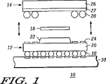
図1には、第1半導体パッケージ12及び重ね合わされる第2半導体パッケージ14を有する積層半導体パッケージ10が示される。第1半導体パッケージ12と第2半導体パッケージ14との間には薄膜材16の形態の介在要素が配置される。薄膜材16の両側(すなわち上面及び下面)には粘着性があり、一形態において粘着剤は熱によって活性化する。膜として、薄膜16は前もって比較的的確な寸法を有する所望の的確な形状に形成することができる。他の種類の粘着剤を使用することもできる。薄膜材16は柔軟性及び適合性(すなわち表面一致性)があり、半導体パッケージによって定義されるどのような厚み、すなわち寸法をも有し得る。第1半導体パッケージ12は、第1半導体パッケージ12内の半導体ダイ(図示略)への電気的接続を行う複数の導電ボールを有している。例えば、導電ボール18はこのような複数の導電ボールのうちの一つである。ここで定義され用いられるように、導電ボールはどのような導電材からも作られる。導電ボールは下部基板、すなわち複数の導電接点を有するマザーボード30上に配置される。また、第1半導体パッケージ12は基板20を有している。基板20は、半導体パッケージ基板に共通して用いられる導電フィルム(すなわち、基板)、FR4、ビスマレイミド/トリアジン(BT)積層板又は他の有機材料のような様々な材料から形成可能である。基板20にはモールドキャップ22が重ね合わされ、その大きさは半導体パッケージ本体の大きさ及び半田ラン24等の近接する半田ランによって決定される。ここで用いられる単語「半田ラン」はいずれの形状の電気接点をも含む。更に、単語「半田」は従来の半田組成に加えて導電ペースト、ポリマーバンプ等の様々な導電材料を含む。モールドキャップ22は一般的に樹脂成形材である。成形が完了すると、基板20及びモールドキャップ22は互いに一体化される。第2半導体パッケージ14もまた導電ボール28のような複数の導電ボールを有している。導電ボールはパッケージ基板27と当接している。半導体パッケージ基板27にはモールドキャップ26が重ね合わされる。成形が完了すると、モールドキャップ26は、パッケージ基板27と一体化される。モールドキャップ26は様々な従来のモールド複合材のうちのいずれかからも形成される。2つの半導体パッケージのみが図示されているが、この構造においていくつの半導体パッケージが積層されても良い。したがって最後、すなわち頂部側半導体パッケージは下側のパッケージ基板における一端から他端へ完全に延びるモールドキャップを有することができる。また、モールドキャップ以外の構造が用いられても良い。例えば、例示されたモールドキャップに代えて、グロブトップ、所定のセラミック中空構造、所定の金属中空構造、ガラス等を用いても良い。また、最後、すなわち頂部側半導体パッケージは下側のパッケージ基板の一端から他端まで延びない構造によって実施されても良い。
In general, there is provided an improved method and apparatus for stacking semiconductor packages having increased thermal and noise characteristics, alignment characteristics, and safety, as opposed to a semiconductor die. Stacking of semiconductor packages can be implemented in various forms, some of which will be described in detail below. FIG. 1 is a stacked semiconductor having a
図2は図1の2つの半導体パッケージの完成したアッセンブリを示している。説明の便宜上、参照符号はこれら図1及び2において同一とする。組み付け方法において、第1半導体パッケージ12はマザーボード30上の所望の所定位置に配置される。第1半導体パッケージ12の導電ボールはマザーボード30の所定の露出接点と直接的に接触するように配置される。マザーボード30は増設構成要素(図示略)に接触する各面から延びる電気配線(図示略)を有する。薄膜材16はその後、第1半導体パッケージ12のモールドキャップ22の上面上に配置される。一般的に、薄膜材16は十分に粘着性があるので、第2半導体パッケージ14が第1半導体パッケージ12の上面に配置された場合に所定位置に留まる。この配設は一般的に自動化されており、ロボット設備によって行われる。一形態において、所定半田リフロー工程に特化される全ての構成要素は、マザーボード上に配置又は密集される。その後、半導体積層パッケージアッセンブリ全体はリフローオーブン(図示略)におけるリフロー工程を通過する。熱が供給されるリフロー工程中において、2つのパッケージはそれら同士が組み合わされるとともに、マザーボード30へ他の構成要素が取り付けられ、且つ薄膜材16は2つの半導体積層パッケージを互いに固着させる。例示した形態において、薄膜材16はリフロー工程の熱の影響によって引き起こされる反りを小さくするとともに、第1半導体パッケージ12を第2半導体パッケージ14に固着し、それらが容易に離間することを妨げる。薄膜材16は両半導体パッケージの露出面に適合し且つ一致する。いくつかの構成において、頂部側すなわち第2半導体パッケージ14の底面はベアシリコンである。最下部側すなわち第1半導体パッケージ12のモールドキャップ22の表面は、成形用プラスチックを含む様々な材料のうちのいずれかであれば良い。したがって、薄膜材16はその特性によって効果的に2つの半導体パッケージに接着し、最終積層パッケージアッセンブリの剛性を増加させる。このような剛性の増加は、接触接合の信頼性を考察すること及び落下試験能力の改善に重要である。
FIG. 2 shows the completed assembly of the two semiconductor packages of FIG. For convenience of explanation, the reference numerals are the same in FIGS. In the assembling method, the
一形態において、第2半導体パッケージ14は不正な検索から保護されるべき保護データを格納するデータ格納又はメモリ集積回路として実施される。例えば、一般的にフラッシュメモリが情報を格納するために使用される。使用者が第2半導体パッケージ14から第1半導体パッケージ12を分離させようとすると、第2半導体パッケージ14は薄膜材16の粘着性により損傷し、メモリ集積回路へはアクセスできず、データをアクセス及び抽出から保護する。したがって、薄膜材16は積層パッケージアッセンブリに剛性を提供することに加えて、データへのアクセスを困難にすることにより機密データの安全性を提供する。
In one form, the
加えて、薄膜材16にRFI及びEMI材を用いた場合、第1半導体パッケージ12と第2半導体パッケージ14との間に電気的シールドが提供される。したがって、近接するパッケージからの干渉信号に対して、近接するノイズ源から薄膜材16によって隔離された電気回路網の部位が保護される。2つの積層半導体パッケージ間における薄膜材の挿入及び一体化は、最下部側又は下側パッケージ位置に配置される高速ロジック集積回路のノイズ低減を可能にする。ノイズ低減性はパッケージアッセンブリの能力全体を向上し、このパッケージを携帯無線製品に見られるような様々なノイズに敏感なアプリケーションに使用可能とする。
In addition, when RFI and EMI materials are used for the
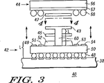
図3には本発明の他の形態に係る積層半導体パッケージアッセンブリ40が示される。導電接点を有するマザーボード30は第1半導体パッケージ42の下側に存在し、該第1半導体パッケージ42は第2半導体パッケージ44の下側に存在する。第1半導体パッケージ42は第1半導体パッケージ42内の半導体ダイ(図示略)への電気的接点を成す複数の導電ボールを有する。例えば、導電ボール48はこのような複数の導電ボールのうちの一つである。上述のように、導電ボールはいかなる導電材からも形成される。導電ボールはマザーボード30の接点上に配置される。第1半導体パッケージ42は基板50を有している。基板50は、導電膜(例えば基板)FR4、ビスマレイミド/トリアジン(BT)積層板又は有機材料のような半導体パッケージ基板に一般的に使用される様々な材料から作られることができる。基板50にはモールドキャップ52が重ね合わされ、その大きさは半導体パッケージ体の大きさ及び近接する半田ラン49,51,53及び54等の半田ランによって決定される。モールドキャップ52は一般的に樹脂成形材である。成形が完了すると、基板50及びモールドキャップ52は互いに一体化される。第2半導体パッケージ44もまた導電ボール58のような複数の導電ボールを有している。導電ボールはパッケージ基板57と当接している。半導体パッケージ基板57にはモールドキャップ56が重ね合わされる。成形が完了すると、モールドキャップ56は、パッケージ基板57と一体化される。2つの半導体パッケージのみが図示されているが、この構造においていくつの半導体パッケージが積層されても良い。また、最後、すなわち頂部側半導体パッケージは、下側のパッケージ基板の一端から他端へ完全に延びるモールドキャップ、又は下側のパッケージの上面に対して類似又は変形した形状を有しても良い。
FIG. 3 shows a stacked
第1半導体パッケージ42と第2半導体パッケージ44との間には、薄膜材45及び47のような挿入部材、及び部材43がノイズ低減及び/又は熱強化を目的として設けられる。図3の部材43は、図示された側部とほぼ垂直な1つ以上の辺上に延長部を有している。延長部は長さLを有するように例示されている。長さLは仕様に応じて変更されることができる。図3の実施形態に示されるように、Lはアッセンブリが形成される時に少なくとも部材43の側部からマザーボード30の上面にまで延びるのに十分な長さとなるように示されている。他の形態において、長さは積層パッケージアッセンブリから横方向に延びるとともに1つ以上の目的のための接点を規定するのに十分な長さで実施されても良く、又はマザーボード30のビアを通って様々に延びるのに十分な長さで実施されても良い。図3から理解できるように、部材43は、下方へ曲げられる場合又は他の構造と接触するように構成される場合のいずれかにおいて、マザーボード30と接触するように積層半導体パッケージアッセンブリ40から外側へ向けて延びている。
Between the
反り又は安全性が懸案事項でない場合、薄膜材45及び47は付加物であると考えることができる。使用される場合の薄膜材の利点は、薄膜材16に関して前述した利点と類似である。例示された形態において、薄膜材45は第1半導体パッケージ42のモールドキャップ52に対して配置され、薄膜材47は第2半導体パッケージ44の底面に対して配置される。薄膜材45及び47は異なる材料組成及び異なる寸法でも良い。
If warpage or safety is not a concern, the
部材43は、積層パッケージアッセンブリの熱特性を強化する目的、及び/又はRFI及びEMI保護及び/又は防護を提供する目的のために、使用に応じて2つの半導体パッケージ42及び44の間、並びに薄膜材45及び47の間に配置される。薄膜材45及び47が使用される場合、この積層半導体パッケージアッセンブリ40の安全性は著しく改善される。部材43は、熱伝導性及びノイズ防護特性の一方又は両方を有する、容易に利用可能な範囲の材料から選択される。この積み上げアッセンブリへの部材43の導入は、従来手段による2つのパッケージ分離を阻止しつつ、底部側パッケージへのアクセスを妨げることによって安全性を改善する。薄膜材45及び47が適切に配置された場合、このパッケージ積層の安全性は著しく強化される。底部側パッケージと部材43、及び頂部側パッケージと部材43という異種部材間の薄膜による接合は、分離を不可能にする。
特に、部材43が表面相互接続又は貫通固定方法のいずれかによってマザーボード30に取り付けられる場合、部材セット間の機械的及び熱的な非類似性は構造を一つに統合する。二つのパッケージを分離しようとする場合、薄膜材45はモールドキャップ52及び部材43への粘着接合材を形成する。薄膜材47は部材43とパッケージ基板57との間に粘着接合材を形成する。2つのパッケージを分離しようとする場合、熱及び機械応力が積層パッケージアッセンブリ構造の分離を妨げる。記載されたような場合において、分離によって積層パッケージアッセンブリは破壊される。したがって、特に集積回路が保護データを含むメモリである場合、集積回路パッケージのうちの一つからのデータの除去は著しい機能障害となる。
In particular, when the
図4は図3の4−4線に沿った平面図であって、部材43の物理的な構成を示している。この構成は上述のように部材43を使用することを可能とする。2辺上に長さLの延長部60が示され、該延長部60は部材43をマザーボード30に装着するのに用いられる。図5に示すように底面の2辺のみに導電ボール58のような導電ボールが密集したパッケージ基板57を有する第2半導体パッケージ44を考慮して、2つの延長部のみが例示される。
4 is a plan view taken along line 4-4 of FIG. 3 and shows a physical configuration of the
図6は図4の部材43が半導体パッケージ44のパッケージ基板57の底面に重ね合わされた状態を示している。例示された形態において、延長部は導電ボールが密集していないパッケージ基板57の底面の2辺から延びるように配置される。延長部60の長さLは変更可能である。延長部60は、半導体パッケージ44から横方向に延びるだけでも良いし、マザーボード30から遠ざかるように上方に向かって、或いはマザーボード30上にまで又はマザーボード30を貫通するように下方に向かって構成されても良い。
FIG. 6 shows a state in which the
図7は、図3の2つの半導体パッケージを含む完成した積層半導体パッケージアッセンブリ40を、第1半導体パッケージ42と第2半導体パッケージとの間に挿入される部材43及び薄膜材45及び47と共に示す側面図である。部材43は介在要素として機能し、下側に存在する基板、すなわちマザーボード30に物理的に接触するように、モールドキャップ52の上方から、半導体パッケージ42から横方向に離れて延びる。延長部の様々な選択肢が存在する。例えば、一形態において、延長部61はマザーボード30の上面に接触する。延長部61への電気的な接触は様々な方法によって行われる。例えば、延長部61はマザーボード30の上面に配置され且つ完成した積層半導体パッケージアッセンブリ40に近接又は一体化された構成要素(図示略)と接触してもよい。他の形態において、部分64によって示される延長部61の延出部は、マザーボード30の背面側へ突出又は貫通する。その結果、延長部61への電気的な接触はマザーボード30の背面側から行われることができる。
FIG. 7 is a side view showing the completed stacked
図8は、図3の4−4線に沿った平面図であって、部材43の更に他の物理的な構成を示している。この構成は、半導体パッケージ44のパッケージ基板57の底面の4辺全てに導電ボールが密集する状況において部材43が使用されることを可能とする。所定長さの4つの延長部60が図示される。互いの長さは同一でも良いし、いくつか又は全てが異なっていても良い。図9に示されるように底面の4辺に導電ボール58のような導電ボールが密集したパッケージ基板57を有する第2半導体パッケージ44を考慮して、4つの延長部が例示される。
FIG. 8 is a plan view taken along line 4-4 in FIG. 3 and shows still another physical configuration of the
図10は、半導体パッケージ44のパッケージ基板57に図8の部材43が重ね合わされた図である。図示された形態において、延長部はパッケージ基板57の底面の4辺全てから延びるように配置されている。一構成において、延長部60は、パッケージ基板57の底面の左側に図示されるように、内側の列のみの導電ボールと接触することができる。例示された形態において、導電ボールは接地電位又はVSS電位である。しかしながら、他の信号電位とすることもできる。他の構成において、延長部62は横方向に隣接する2つの導電ボールを捕捉するとともに、所定量だけ半導体パッケージ44を越えて突出してもよい。横方向に隣接する2つの導電ボールは、それぞれが接地電位又はVSS電位、或いは他の電位のような同じ電位に接続される。他の構成において、延長部63は横方向に隣接する2つの導電ボールを捕捉するのに十分なだけの長さである。この場合も、2つの横方向に隣接する導電ボールは、それぞれが接地電位又はVSS電位、或いは他の電位のような同じ電位に接続される。これらのような構造の変形例は容易に考えられる。例えば、半導体パッケージ44の側部上の横方向の導電ボールの数は異なっても良いし、2列又は2行よりも多くしても良い。延長部62の長さLは変更されてもよい。また、延長部62は半導体パッケージ44から横方向に延びるだけでも良いし、マザーボード30から離間するように上方に向けて、或いはマザーボード30上にまで又はマザーボード30を貫通するように下方に向けて構成されても良い。
FIG. 10 is a diagram in which the
図11は、図8に示される部材43を用いた図3の2つの半導体パッケージの完成アッセンブリを示す。説明の便宜上、参照符号はこれら両図において同一とする。組み付け方法において、第1半導体パッケージ42はマザーボード30上の所望の所定位置に配置される。そして薄膜材45は第1半導体パッケージ42のモールドキャップ52の上面に配置される。一般的に、薄膜材45は十分に粘着性があるので、部材43が薄膜材45の上面に配置された場合に所定位置に留まる。そして薄膜材47は部材43の上面に配置される。そして第2半導体パッケージ44の底面は薄膜材47と当接するように配置される。全ての配設は一般的に自動化されており、ロボット設備によって行われる。一形態において、所定半田リフロー工程に特化される全ての構成要素は、マザーボード上に配置又は密集される。その後、半導体積層パッケージアッセンブリ全体はリフローオーブン(図示略)におけるリフロー工程を通過する。リフロー工程中において、2つのパッケージ及び部材43はマザーボード30に設けられる他の構成要素と共に薄膜材45及び47によって所定位置に固着される。半導体パッケージ44及び42は導電ボールを介して互いに取り付けられる。例示された形態において、薄膜材45及び47はリフロー工程の熱の影響によって引き起こされる反りを小さくする。また、薄膜材45及び47は、半導体パッケージ42及び半導体パッケージ44を部材43に固着し、それらが容易に離間することを妨げる。加えて、部材43は半導体パッケージアッセンブリへの熱及び/又はノイズ強化を提供する。薄膜材45及び47は両半導体パッケージ及び部材43の露出面に適合し且つ一致する。部材43,45及び47は同じ材料でも良いし、同じ組成を有しても良い。いくつかの構成において、頂部側半導体パッケージ44の底面はベアシリコンである。底部側半導体パッケージ42のモールドキャップ52の表面は、成形用プラスチックを含む様々な材料のうちのいずれかであれば良い。したがって、薄膜材45及び47の特性は2つの半導体パッケージを部材43に接着し、最終積層パッケージアッセンブリの剛性を増加させる。
FIG. 11 shows a completed assembly of the two semiconductor packages of FIG. 3 using the
図11に例示された形態において、延長部60は終端までに内側の列の導電ボールを1つだけ捕捉する。したがって、半導体パッケージ42及び半導体パッケージ44の端部を越える部材43の延長部は表現されていない。半田ラン51及び半田ラン53はそれぞれ半田ラン49及び半田ラン54よりも薄く、部材43への連結部を収容する。一形態において、半田ラン49及び半田ラン54の薄層化はエッチングによって達成される。他の形態において、厚みの増減は従来の半田マスク技術によって達成されても良い。
In the form illustrated in FIG. 11, the
図11の積層パッケージアッセンブリの変形例が形成されても良い。例えば、延長部60はいずれの半田ランと導電バンプとの間にも配置されなくて良い。このような実施において、下側半導体パッケージのモールドキャップに近接する半田ラン及び導電バンプは、延長部用空間から離れるように更に遠くへ押圧され、基板50の上面に直接接続される。一形態において、延長部60は、モールドキャップ52を360度完全に囲む材料の連続片として実施されても良い。したがって、完全な包囲延長部60はドーム形状を有している。この形態において、ノイズ防護は、モールドキャップを完全に囲む半導体パッケージ及び積層パッケージアッセンブリの縁部の内側に留まる延長部60によって得られる。他の形態において、延長部60は長方形又は箱型を成すように構成される。更に他の形態において、延長部60は1つの辺にのみ沿って延びるように、1つの辺の一部に沿って延びるように、又はモールドキャップ52の全ての辺よりも少ない辺に沿って延びるように構成される。これらの形態において、一般的に延長部60はモールドキャップ52と形状において一致するが、必ずしも一致する必要はない。他の形態において、モールドキャップに隣接する導電バンプの横列の数は、例示されている数と別の数となるように実施されても良い。図11に示された形態において、2列の導電バンプが提供されている。しかしながら、1列のみ、3列又はそれ以上を備えても良い。
A variation of the stacked package assembly of FIG. 11 may be formed. For example, the
図12は、部材43が2つの半導体パッケージ間を横方向に突出するとともに、積層半導体パッケージアッセンブリ40の外側で上方へ曲折された積層半導体パッケージアッセンブリ40の他の形態を示す。この構成の部材43は1つ以上の目的を達成するために機能することができる。特に、外気への露出は熱散逸を強化する熱分散特性として機能する。加えて、部材43は導電材であるので、部材43が積層半導体パッケージアッセンブリ40の外部に位置することは、部材43が積層半導体パッケージアッセンブリ40の所定箇所を電気的に防護することを許容する。部材43が上方に曲折していることに加えて、部材43が外部に露出していることにより、部材43への接地電位又は他の電圧の接触をどの様に達成するかについて、使用者は柔軟に対処できる。他の形態において、部材43は曲折されなくても良く、熱散逸強化又は電気接触の目的のために積層半導体パッケージアッセンブリ40から横方向に延びることが許容されなくても良い。さらに、例示された90度に加えて、部材43を形成する他の角度が用いられても良い。
FIG. 12 shows another form of the stacked
図13は図12に示された積層半導体パッケージアッセンブリ40の側面図を示す。図には部材43を用いた単体フィン構造が示されている。この方法の熱散逸特性を更に強化するために、増設フィン(図示略)が付加されても良い。また、図13では略90度に曲折した例が示されているが、使用に応じてどのような角度に曲折しても良い。
FIG. 13 is a side view of the stacked
図14は、前述の図11の説明の積層パッケージアッセンブリの変形例のうちの1つである。説明の便宜上、図11の構成要素に類似している図14の構成要素には同様の符号が付される。図14に例示された形態において、延長部60は図11に示される導電ボールと半田ランとの間を延びていない。正しくは、延長部60は、基板50に対して少なくとも1つの物理的又は電気的接点を備えることにより基板50と物理的に当接している。半田ラン及び導電ボールは、積層パッケージアッセンブリの中央部から位置ずれしており、延長部60が半田ラン又は導電ボールと当接せずに基板50と当接できるだけの空間が提供される。図14に例示された形態において、延長部60は効果的にモールドキャップを取り囲み、防護性を提供する。
FIG. 14 is one of the modified examples of the stacked package assembly described with reference to FIG. For convenience of explanation, the components in FIG. 14 that are similar to the components in FIG. In the form illustrated in FIG. 14, the
図15は、図14の積層パッケージアッセンブリの頂部側半導体パッケージの底面図を示している。接触領域65はパッケージ基板57を包囲するように例示されている。例示された形態において、接触領域65は長方形であるが、他の形状が用いられても良い。接触領域65は、延長部60が接触する基板50の領域と重なり合う所定領域である。加えて、下側半導体パッケージと接触する延長部60に代えて、延長部60は接触領域65によって画定された領域内で頂部側半導体パッケージと接触することができるように、上方に傾斜させられても良い。導電ボール58のような導電ボールを増設又は減少させても良い。
FIG. 15 shows a bottom view of the top semiconductor package of the stacked package assembly of FIG. The
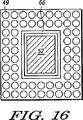
図16は、図14の積層パッケージアッセンブリの底部又は下側半導体パッケージを示す平面図である。接触領域66はモールドキャップ52を包囲するように示されている。接触領域66は、延長部60が接触する基板50上の所定領域である。図15と関連して、導電ボールの総数を変更しても良い。延長部60が覆うモールドキャップ52の周囲の量は、1辺分の割合から全周囲までの範囲で変更されても良い。
16 is a plan view showing the bottom or lower semiconductor package of the stacked package assembly of FIG. Contact area 66 is shown surrounding the
以上によって、積層半導体パッケージ及びその形成方法が提供されたことが理解されるであろう。ここで記載されているように複数の集積回路パッケージが積層することにより、パッケージ剛性が増加され、これにより製造歩留まりが向上する。また、不正な検索からのデータ安全性の強化、熱強化及びノイズ低減が提供される。 It will be understood that a stacked semiconductor package and a method for forming the same have been provided. Stacking a plurality of integrated circuit packages as described herein increases package rigidity and thereby improves manufacturing yield. It also provides enhanced data safety from unauthorized searches, enhanced heat and reduced noise.
一形態において、積層半導体構造が提供される。第1半導体パッケージは第1面及び第2面を備える。前記第1面は該第1面に設けられて前記第1半導体パッケージへの電気的接続を行う複数の第1導電バンプを有し、前記第1面の反対側にある非平面状の前記第2面はモールドキャップ及び隣接する複数の半田ランを有する。第2半導体パッケージは前記第1半導体パッケージに重なり合う。前記第2半導体パッケージは第1面及び該第1面の反対側にある第2面を備え、その第2面は該第2面の中央部の外側に位置して前記第1半導体パッケージの前記複数の半田ランと接触する複数の第2導電バンプを有し、前記第2半導体パッケージは複数の第2導電バンプを介して前記第1半導体パッケージと直接的な電気的接触を行う。介在要素は、前記第1半導体パッケージと前記第2半導体パッケージとの間に直接接触するように配置される。前記介在要素は前記第1半導体パッケージ及び前記第2半導体パッケージの各々並びに前記介在要素に接触する前記第2半導体パッケージに接着するのに十分な粘着性を有し、前記介在要素は前記第1半導体パッケージ及び前記第2半導体パッケージに対して表面適合性を有する。下部基板は複数の接点を有する。前記下部基板における前記複数の接点の各々は前記第1半導体パッケージにおける前記複数の第1導電バンプのうちの少なくとも1つに接触する。 In one form, a stacked semiconductor structure is provided. The first semiconductor package includes a first surface and a second surface. The first surface has a plurality of first conductive bumps provided on the first surface for electrical connection to the first semiconductor package, and the non-planar first surface on the opposite side of the first surface. The two surfaces have a mold cap and a plurality of adjacent solder runs. The second semiconductor package overlaps the first semiconductor package. The second semiconductor package includes a first surface and a second surface opposite to the first surface, and the second surface is located outside a center portion of the second surface and the second surface of the first semiconductor package. The second semiconductor package has a plurality of second conductive bumps in contact with the plurality of solder runs, and the second semiconductor package makes direct electrical contact with the first semiconductor package through the plurality of second conductive bumps. The interposition element is disposed so as to be in direct contact between the first semiconductor package and the second semiconductor package. The interposition element has sufficient adhesiveness to adhere to each of the first semiconductor package and the second semiconductor package and the second semiconductor package in contact with the interposition element, and the interposition element is the first semiconductor Surface compatible with the package and the second semiconductor package. The lower substrate has a plurality of contacts. Each of the plurality of contacts on the lower substrate contacts at least one of the plurality of first conductive bumps on the first semiconductor package.
一形態において、前記介在要素は熱活性材である。前記介在要素は破断することなく形成するのに十分な可塑性を有する。他の形態において、前記第2半導体パッケージは、保護データを格納するデータ格納集積回路である。他の形態において、前記介在要素は前記第1半導体パッケージ及び前記第2半導体パッケージの周囲から外側に向けて横方向に延びる。更に他の形態において、前記介在要素は、前記第1半導体パッケージ及び前記第2半導体パッケージの周囲から外側に向けて横方向に延びるとともに、下部基板から離間する方向に曲げられる。更に他の形態において、前記介在要素は、前記第1半導体パッケージ及び前記第2半導体パッケージの周囲から外側に向けて横方向に延びるとともに、前記下部基板に向かって電気的接触を行うように曲げられる。更に他の形態において、前記介在要素は、前記下部基板への電気的接触が行われる場合に、導電端子又は絶縁端子のうちの少なくとも1つに接続される。前記導電端子は基準電圧端子、電力供給端子、接地端子、信号端子又は他の種類の端子でも良い。絶縁端子はハウジング端子、ケーシング端子、搭載金具、酸化物又は窒化物のような絶縁材への接続部、又は他の種類の非導電端子でも良い。更なる形態において、前記介在要素は、前記第1半導体パッケージ及び前記第2半導体パッケージの周囲から外側に向けて横方向に延びるとともに、電気的又は物理的接触のうちの一方を前記下部基板の背面側から行うために前記下部基板に向かって且つ同下部基板を通過するように曲げられる。更に他の形態において、前記第2面の中央部の外側に位置する前記第2半導体パッケージの前記複数の第2導電バンプは、前記第2面において互いに反対側に位置する2辺のみに沿って配置され、前記介在要素は前記第2面において前記2辺と隣接して互いに反対側に位置する2辺から、前記積層半導体パッケージアッセンブリの横方向に延びる。他の形態において、前記介在要素は、前記積層半導体パッケージアッセンブリのノイズ隔離及び熱強化のために、前記下部基板と物理的に接触するように前記モールドキャップ上から延びる。 In one form, the intervening element is a thermally activated material. The intervening elements are sufficiently plastic to form without breaking. In another embodiment, the second semiconductor package is a data storage integrated circuit that stores protection data. In another embodiment, the interposition element extends laterally outward from the periphery of the first semiconductor package and the second semiconductor package. In still another embodiment, the interposition element extends laterally outward from the periphery of the first semiconductor package and the second semiconductor package and is bent in a direction away from the lower substrate. In still another embodiment, the interposition element extends laterally outward from the periphery of the first semiconductor package and the second semiconductor package and is bent to make electrical contact toward the lower substrate. . In yet another form, the interposition element is connected to at least one of a conductive terminal or an insulated terminal when electrical contact is made to the lower substrate. The conductive terminal may be a reference voltage terminal, a power supply terminal, a ground terminal, a signal terminal, or other types of terminals. The insulated terminals may be housing terminals, casing terminals, mounting hardware, connections to insulating materials such as oxides or nitrides, or other types of non-conductive terminals. In a further form, the interposition element extends laterally from the periphery of the first semiconductor package and the second semiconductor package toward the outside, and one of electrical or physical contact is provided on the back surface of the lower substrate. In order to perform from the side, it is bent toward the lower substrate and through the lower substrate. In still another embodiment, the plurality of second conductive bumps of the second semiconductor package located outside the central portion of the second surface are along only two sides located on opposite sides of the second surface. The interposition element extends in the lateral direction of the stacked semiconductor package assembly from two sides located adjacent to the two sides and opposite to each other on the second surface. In another embodiment, the interposition element extends from the mold cap so as to be in physical contact with the lower substrate for noise isolation and thermal enhancement of the stacked semiconductor package assembly.
更なる形態において、積層半導体パッケージアッセンブリは第1面及び第2面を有する第1半導体パッケージを備える。前記第1面は前記第1半導体パッケージへの電気的接続を行う複数の第1接点を有する。前記第1面の反対側にある前記第2面は複数の第2接点を有する。第2半導体パッケージは前記第1半導体パッケージの上に配置され、第1面及び該第1面の反対側にある第2面を備える。前記第2面は該第2面上に位置する複数の第3接点を有し、該複数の第3接点はそれぞれ前記第1半導体パッケージの前記複数の第2接点と接触する。前記第2半導体パッケージは前記第1半導体パッケージと直接的な電気的接触を行う。介在要素は前記第1半導体パッケージの一部と前記第2半導体パッケージとの間に直接接触するように配置される。前記介在要素は前記第1半導体パッケージ及び前記第2半導体パッケージの各々に接着し且つ前記介在要素に接触する前記第1半導体パッケージ及び前記第2半導体パッケージの隣接面に剛性を提供するのに十分な粘着性を有する。前記介在要素は前記第1半導体パッケージ及び前記第2半導体パッケージに対して表面適合性を有するとともに、前記積層半導体パッケージアッセンブリの周囲から横方向に延びる部位を有する。下部基板は複数の第4接点を有する。前記基板における前記複数の第4接点の各々は前記第1半導体パッケージにおける前記複数の第1接点のうちの少なくとも1つに接触する。 In a further form, the stacked semiconductor package assembly comprises a first semiconductor package having a first surface and a second surface. The first surface has a plurality of first contacts for electrical connection to the first semiconductor package. The second surface on the opposite side of the first surface has a plurality of second contacts. The second semiconductor package is disposed on the first semiconductor package, and includes a first surface and a second surface opposite to the first surface. The second surface has a plurality of third contacts located on the second surface, and the plurality of third contacts respectively contact the plurality of second contacts of the first semiconductor package. The second semiconductor package makes direct electrical contact with the first semiconductor package. The interposition element is disposed so as to be in direct contact between a part of the first semiconductor package and the second semiconductor package. The interposition element is sufficient to adhere to each of the first semiconductor package and the second semiconductor package and to provide rigidity to adjacent surfaces of the first semiconductor package and the second semiconductor package that contact the interposition element. Adhesive. The intervening element has surface compatibility with the first semiconductor package and the second semiconductor package, and has a portion extending laterally from the periphery of the stacked semiconductor package assembly. The lower substrate has a plurality of fourth contacts. Each of the plurality of fourth contacts on the substrate contacts at least one of the plurality of first contacts on the first semiconductor package.
一形態において、前記介在要素は下部基板から離間する方向に曲げられる。他の形態において、前記介在要素は、前記第1半導体パッケージ及び前記第2半導体パッケージの周囲から外側に向けて横方向に延びるとともに、前記下部基板に向かって電気的接触を行うように曲げられる。更に他の形態において、前記介在要素は、前記下部基板への電気的接触が行われる場合に、定電圧端子に接続される。 In one form, the interposition element is bent in a direction away from the lower substrate. In another embodiment, the interposition element extends laterally outward from the periphery of the first semiconductor package and the second semiconductor package and is bent to make electrical contact toward the lower substrate. In yet another embodiment, the interposition element is connected to a constant voltage terminal when electrical contact is made to the lower substrate.
更に別の形態において、本願では第1半導体パッケージを備える積層半導体パッケージアッセンブリが提供される。第1半導体パッケージの第1面は、該第1面に設けられて前記第1半導体パッケージへの電気的接続を行う複数の第1導電バンプを有する。前記第1半導体パッケージは、モールドキャップ及び隣接する複数の半田ランを有し前記第1面の反対側にある非平面状の前記第2面を備える。第2半導体パッケージは、前記第1半導体パッケージに重なり合い、第1面及び該第1面の反対側にある第2面を備える。前記第2面は該第2面の中央部の外側に位置して前記第1半導体パッケージの前記複数の半田ランと電気的に接触する複数の第2導電バンプを有する。前記第2半導体パッケージは複数の第2導電バンプを介して前記第1半導体パッケージと電気的接触を行う。伝導粘着層は、前記積層半導体パッケージアッセンブリの中央領域に配置され且つ前記第1半導体パッケージと前記第2半導体パッケージとの間に直接接触する。前記伝導粘着層の一部は前記中央領域から延びるとともに前記複数の第1接点のうちの少なくとも1つ及び前記複数の第2接点のうちの1つの間にあり且つ電気的に接触する。下部基板は複数の接点を有する。前記下部基板における前記複数の接点の各々は前記第1半導体パッケージにおける前記複数の第1導電バンプのうちの少なくとも1つに接触する。 In yet another aspect, the present application provides a stacked semiconductor package assembly comprising a first semiconductor package. The first surface of the first semiconductor package has a plurality of first conductive bumps provided on the first surface and making electrical connection to the first semiconductor package. The first semiconductor package includes a non-planar second surface having a mold cap and a plurality of adjacent solder runs on the opposite side of the first surface. The second semiconductor package includes a first surface and a second surface that is opposite to the first surface and overlaps the first semiconductor package. The second surface has a plurality of second conductive bumps that are located outside a central portion of the second surface and are in electrical contact with the plurality of solder runs of the first semiconductor package. The second semiconductor package is in electrical contact with the first semiconductor package through a plurality of second conductive bumps. The conductive adhesive layer is disposed in a central region of the stacked semiconductor package assembly and is in direct contact between the first semiconductor package and the second semiconductor package. A portion of the conductive adhesive layer extends from the central region and is in electrical contact with at least one of the plurality of first contacts and one of the plurality of second contacts. The lower substrate has a plurality of contacts. Each of the plurality of contacts on the lower substrate contacts at least one of the plurality of first conductive bumps on the first semiconductor package.
一形態において、前記第1半導体パッケージと前記第2半導体パッケージとの間の電気的防護又は熱散逸のうちの少なくとも1つを強化するために、前記複数の第1接点のうちの少なくとも1つ及び前記複数の第2接点のうちの1つは定電圧端子と接続される。更に他の形態において、前記伝導粘着層は、熱活性及び可塑性を有する膜である。更なる形態において、前記第2半導体パッケージは、保護データを格納するデータ格納集積回路である。また更なる形態において、前記中央領域から延びる伝導粘着層の部位は、前記複数の半田ラン及び前記複数の第2導電バンプの幾つかの間を、前記積層半田パッケージアッセンブリの少なくとも2辺に向かって横方向に延びる。更なる別の形態において、前記伝導粘着層の第2部位は、前記積層半導体パッケージアッセンブリの外縁を越えて横方向に延びる。 In one aspect, at least one of the plurality of first contacts and the at least one of the plurality of first contacts to enhance at least one of electrical protection or heat dissipation between the first semiconductor package and the second semiconductor package; One of the plurality of second contacts is connected to a constant voltage terminal. In still another embodiment, the conductive adhesive layer is a film having thermal activity and plasticity. In a further aspect, the second semiconductor package is a data storage integrated circuit that stores protection data. In a still further embodiment, the conductive adhesive layer extending from the central region has a lateral direction between some of the plurality of solder runs and the plurality of second conductive bumps toward at least two sides of the multilayer solder package assembly. Extend to. In yet another embodiment, the second portion of the conductive adhesive layer extends laterally beyond the outer edge of the stacked semiconductor package assembly.
上記説明において、本発明は具体的な実施形態を参照して記述された。しかしながら、当業者には、後の請求の範囲に規定される本発明の範囲から逸脱しない限り様々な改良及び変更を行うことができることが理解できる。例えば、部材16,45及び47の薄膜材を例示して記述したが、厚みが変更された部材を用いることができることが理解され、産業上の「薄膜」と見なしたり分類したりする必要は全くない。本願において電気的に又は熱的に伝導性があると記載される構成要素のそれぞれ及び全てに様々な伝導材を用いることができる。積層される半導体パッケージとして、様々な半導体封止材を用いることができる。例えば、樹脂成形化合物、セラミック及び他の半導体材料を用いることができる。積層される半導体装置の数はいくつでも良い。本願に記載された積層半導体パッケージアッセンブリは、ボール・グリッド・アレイ・パッケージズに加えて、鉛半導体パッケージ、ダイレクト・チップ・アタッチ(DCA)フリップ・チップ・デバイス、ランド・グリッド・アレイズ(LGAs)及びリードレス・チップ・キャリアズ(LCCs)と組み合わせて使用することもできる。したがって、明細書及び図面は限定的な意図ではなく例示であると見なされ、このような変更の全てが本発明の範囲に含まれるように意図されている。
In the foregoing description, the invention has been described with reference to specific embodiments. However, one of ordinary skill in the art appreciates that various modifications and changes can be made without departing from the scope of the present invention as set forth in the claims below. For example, although the thin film material of the
特定の実施形態を参照しながら種々の利益、種々の他の利点及び問題の解決方法を説明してきたが、このような種々の利益、種々の他の利点、問題の解決方法および任意の利益、利点または問題の解決方法を実行し、より優れたものにすることができる任意の要素は、請求項のいずれかまたはすべての重要で、必要なまたは不可欠な機能または要素であると解釈すべきではない。 While various benefits, various other advantages, and solutions to problems have been described with reference to particular embodiments, such various benefits, various other advantages, solutions to problems, and any benefits, Any element that can perform an advantage or solve a problem and make it better should not be construed as an important, necessary or essential function or element of any or all of the claims. Absent.
Claims (5)
第2半導体パッケージを前記第1半導体パッケージの上に重ねるように配置することであって、前記第2半導体パッケージは第1面及び該第1面の反対側にある第2面を備え、前記第2面は該第2面の中央部の外側に位置して前記第1半導体パッケージの前記隣接する複数の半田ランと接触する第2の複数の導電バンプを有することと、
介在要素を前記第1半導体パッケージと前記第2半導体パッケージとの間に直接接触するように配置することであって、前記介在要素は前記第1半導体パッケージ及び前記第2半導体パッケージの各々に接着し且つ前記介在要素に接触する前記第1半導体パッケージ及び前記第2半導体パッケージの隣接面に剛性を提供するのに十分な粘着性を有することと、
前記介在要素を前記第1半導体パッケージ及び前記第2半導体パッケージの少なくとも一つの周囲の外側へ横方向に延出させるとともに前記介在要素を一つの角度に曲折させることと、
前記第2の複数の導電バンプ及び前記半田ランを介して、前記第1半導体パッケージと前記第2半導体パッケージとの間の直接的な電気的接触を行うことと、
下部基板を前記第1半導体パッケージに接続することであって、前記下部基板は複数の接点を有し、各接点を前記第1半導体パッケージの前記第1の複数の導電バンプのうちの少なくとも1つに接触させることと、
を備える半導体パッケージの積層方法。Preparing a first semiconductor package comprising a first surface and a second surface, wherein the first surface is provided on the first surface and is electrically connected to the first semiconductor package; The non-planar second surface on the opposite side of the first surface having conductive bumps has a mold cap and a plurality of adjacent solder runs ;
The method comprising: disposing the second semiconductor package to overlap on the first semiconductor package and the second semiconductor package comprises a second surface opposite the first surface and the first surface, said first The second surface has a second plurality of conductive bumps located outside the central portion of the second surface and in contact with the plurality of adjacent solder runs of the first semiconductor package ;
Adhesive intervening elements was to place in direct contact between the first semiconductor package and the second semiconductor package, wherein the intervening element to each of the first semiconductor package and the second semiconductor package And having sufficient adhesiveness to provide rigidity to adjacent surfaces of the first and second semiconductor packages that are in contact with the intervening elements;
And thereby bent the intervening elements in one angular said intervening elements causes extend laterally outward of at least one periphery of said first semiconductor package and the second semiconductor package,
Through the second plurality of conductive bumps and the solder run, and to perform a direct electrical contact between the first semiconductor package and the second semiconductor package,
Connecting a lower substrate to the first semiconductor package, the lower substrate having a plurality of contacts, each contact being at least one of the first plurality of conductive bumps of the first semiconductor package; Contacting with
A method for stacking semiconductor packages comprising:
前記下部基板に向かって且つ同下部基板を通過するように前記介在要素を曲折することと、
前記介在要素に電気的又は物理的接触のうちの少なくとも一方を前記下部基板の背面側から行うことと、
を更に備える請求項1に記載の方法。 And it is bent causes extending the intervening elements one along the outside of said first semiconductor package and the second semiconductor package,
Bending the interposition element toward and through the lower substrate;
Performing at least one of electrical or physical contact with the interposition element from the back side of the lower substrate;
The method of claim 1, further comprising:
前記第1半導体パッケージに重なり合う第2半導体パッケージであって、前記第2半導体パッケージは第1面及び該第1面の反対側にある第2面を備え、その第2面は該第2面の中央部の外側に位置して前記第1半導体パッケージの前記隣接する複数の電気的接点と接触する複数の第2導電バンプを有し、前記第2半導体パッケージは複数の第2導電バンプを介して前記第1半導体パッケージと直接的な電気的接触を行うことと、
前記第1半導体パッケージと前記第2半導体パッケージとの間に直接接触するように配置される介在要素であって、前記介在要素は前記第1半導体パッケージ及び前記第2半導体パッケージの各々に接着し且つ前記介在要素に接触する前記第1半導体パッケージ及び前記第2半導体パッケージの隣接面に剛性を提供するのに十分な粘着性を有し、前記介在要素は前記第1半導体パッケージ及び前記第2半導体パッケージに対して表面適合性を有し、前記介在要素は前記第1半導体パッケージ及び前記第2半導体パッケージの少なくとも一つの周囲の外側へ横方向に延出するとともに所定量だけ曲折することと、
複数の接点を有する下部基板であって、前記下部基板における前記複数の接点の各々は前記第1半導体パッケージにおける前記複数の第1導電バンプのうちの少なくとも1つに接触することと、
を備える積層半導体パッケージアッセンブリ。 A first semiconductor package having a first surface and a second surface, wherein the first surface has a plurality of first conductive bumps provided on the first surface for electrical connection to the first semiconductor package. The non-planar second surface opposite the first surface has a mold cap and a plurality of adjacent electrical contacts;
A second semiconductor package overlapping the first semiconductor package, the second semiconductor package comprising a first surface and a second surface opposite to the first surface, the second surface of the second surface being A plurality of second conductive bumps located on the outside of the central portion and in contact with the plurality of adjacent electrical contacts of the first semiconductor package, wherein the second semiconductor package is interposed via the plurality of second conductive bumps; Making direct electrical contact with the first semiconductor package;
An interposition element disposed in direct contact between the first semiconductor package and the second semiconductor package, the interposition element being bonded to each of the first semiconductor package and the second semiconductor package; The first semiconductor package and the second semiconductor package have sufficient adhesiveness to provide rigidity to adjacent surfaces of the first semiconductor package and the second semiconductor package in contact with the intermediate element, and the intermediate element has the first semiconductor package and the second semiconductor package. The intervening element extends laterally outwardly around at least one of the first semiconductor package and the second semiconductor package and bends by a predetermined amount;
A lower substrate having a plurality of contacts, each of the plurality of contacts in the lower substrate contacting at least one of the plurality of first conductive bumps in the first semiconductor package;
A laminated semiconductor package assembly comprising:
Applications Claiming Priority (3)
| Application Number | Priority Date | Filing Date | Title |
|---|---|---|---|
| US11/108,223 US7196427B2 (en) | 2005-04-18 | 2005-04-18 | Structure having an integrated circuit on another integrated circuit with an intervening bent adhesive element |
| US11/108,223 | 2005-04-18 | ||
| PCT/US2006/006426 WO2006112949A2 (en) | 2005-04-18 | 2006-02-23 | Structure for stacking an integrated circuit on another integrated circuit |
Publications (3)
| Publication Number | Publication Date |
|---|---|
| JP2008537333A JP2008537333A (en) | 2008-09-11 |
| JP2008537333A5 JP2008537333A5 (en) | 2009-04-16 |
| JP4768012B2 true JP4768012B2 (en) | 2011-09-07 |
Family
ID=37107719
Family Applications (1)
| Application Number | Title | Priority Date | Filing Date |
|---|---|---|---|
| JP2008506456A Expired - Fee Related JP4768012B2 (en) | 2005-04-18 | 2006-02-23 | Layered structure of integrated circuits on other integrated circuits |
Country Status (5)
| Country | Link |
|---|---|
| US (1) | US7196427B2 (en) |
| EP (1) | EP1875503A4 (en) |
| JP (1) | JP4768012B2 (en) |
| KR (1) | KR101237669B1 (en) |
| WO (1) | WO2006112949A2 (en) |
Families Citing this family (24)
| Publication number | Priority date | Publication date | Assignee | Title |
|---|---|---|---|---|
| JP4508016B2 (en) * | 2005-07-07 | 2010-07-21 | パナソニック株式会社 | Component mounting method |
| US7923830B2 (en) * | 2007-04-13 | 2011-04-12 | Maxim Integrated Products, Inc. | Package-on-package secure module having anti-tamper mesh in the substrate of the upper package |
| US7868441B2 (en) * | 2007-04-13 | 2011-01-11 | Maxim Integrated Products, Inc. | Package on-package secure module having BGA mesh cap |
| JP2008277457A (en) * | 2007-04-27 | 2008-11-13 | Matsushita Electric Ind Co Ltd | Multilayer semiconductor device and package |
| US7923808B2 (en) * | 2007-11-20 | 2011-04-12 | International Business Machines Corporation | Structure of very high insertion loss of the substrate noise decoupling |
| CN101924041B (en) * | 2009-06-16 | 2015-05-13 | 飞思卡尔半导体公司 | Method for assembling stackable semiconductor packaging |
| US8314486B2 (en) * | 2010-02-23 | 2012-11-20 | Stats Chippac Ltd. | Integrated circuit packaging system with shield and method of manufacture thereof |
| US8299595B2 (en) * | 2010-03-18 | 2012-10-30 | Stats Chippac Ltd. | Integrated circuit package system with package stacking and method of manufacture thereof |
| US8569869B2 (en) * | 2010-03-23 | 2013-10-29 | Stats Chippac Ltd. | Integrated circuit packaging system with encapsulation and method of manufacture thereof |
| US8553420B2 (en) | 2010-10-19 | 2013-10-08 | Tessera, Inc. | Enhanced stacked microelectronic assemblies with central contacts and improved thermal characteristics |
| US8633576B2 (en) | 2011-04-21 | 2014-01-21 | Tessera, Inc. | Stacked chip-on-board module with edge connector |
| US9013033B2 (en) | 2011-04-21 | 2015-04-21 | Tessera, Inc. | Multiple die face-down stacking for two or more die |
| US8952516B2 (en) | 2011-04-21 | 2015-02-10 | Tessera, Inc. | Multiple die stacking for two or more die |
| US8304881B1 (en) | 2011-04-21 | 2012-11-06 | Tessera, Inc. | Flip-chip, face-up and face-down wirebond combination package |
| US8928153B2 (en) | 2011-04-21 | 2015-01-06 | Tessera, Inc. | Flip-chip, face-up and face-down centerbond memory wirebond assemblies |
| US8970028B2 (en) | 2011-12-29 | 2015-03-03 | Invensas Corporation | Embedded heat spreader for package with multiple microelectronic elements and face-down connection |
| US8492888B2 (en) | 2011-09-02 | 2013-07-23 | Stats Chippac Ltd. | Integrated circuit packaging system with stiffener and method of manufacture thereof |
| JP6091053B2 (en) * | 2011-09-14 | 2017-03-08 | キヤノン株式会社 | Semiconductor device, printed circuit board and electronic product |
| CN102522380B (en) * | 2011-12-21 | 2014-12-03 | 华为技术有限公司 | PoP packaging structure |
| US9016552B2 (en) * | 2013-03-15 | 2015-04-28 | Sanmina Corporation | Method for forming interposers and stacked memory devices |
| US9484327B2 (en) * | 2013-03-15 | 2016-11-01 | Qualcomm Incorporated | Package-on-package structure with reduced height |
| CN104795368B (en) * | 2014-01-17 | 2017-10-20 | 日月光半导体制造股份有限公司 | Semiconductor package and semiconductor technology |
| US9543170B2 (en) | 2014-08-22 | 2017-01-10 | Taiwan Semiconductor Manufacturing Company, Ltd. | Semiconductor packages and methods of forming the same |
| US10121766B2 (en) | 2016-06-30 | 2018-11-06 | Micron Technology, Inc. | Package-on-package semiconductor device assemblies including one or more windows and related methods and packages |
Citations (4)
| Publication number | Priority date | Publication date | Assignee | Title |
|---|---|---|---|---|
| JPH09283697A (en) * | 1996-04-18 | 1997-10-31 | Nec Corp | Stack module |
| JPH11330306A (en) * | 1998-04-08 | 1999-11-30 | Anam Semiconductor Inc | Semiconductor package |
| JP2004111656A (en) * | 2002-09-18 | 2004-04-08 | Nec Electronics Corp | Semiconductor device and manufacturing method of semiconductor device |
| JP2006059871A (en) * | 2004-08-17 | 2006-03-02 | Matsushita Electric Ind Co Ltd | Semiconductor device and its manufacturing method |
Family Cites Families (82)
| Publication number | Priority date | Publication date | Assignee | Title |
|---|---|---|---|---|
| DE2608689A1 (en) * | 1976-03-03 | 1977-09-15 | Bosch Gmbh Robert | ELECTRIC MACHINE |
| US4355496A (en) * | 1978-03-31 | 1982-10-26 | Systemation Inc. | Wrapping machine and method |
| US4283903A (en) * | 1978-11-21 | 1981-08-18 | Mayhall Riley H | Package wrapping machine |
| US4522888A (en) * | 1980-12-29 | 1985-06-11 | General Electric Company | Electrical conductors arranged in multiple layers |
| US4670347A (en) * | 1986-03-12 | 1987-06-02 | Topflight Corp. | RFI/EMI shielding apparatus |
| US4699830A (en) * | 1986-06-30 | 1987-10-13 | Baxter Travenol Laboratories, Inc. | Laminated sheet material for packaging electronic components |
| US4770921A (en) * | 1986-09-11 | 1988-09-13 | Insulating Materials Incorporated | Self-shielding multi-layer circuit boards |
| US4813495A (en) * | 1987-05-05 | 1989-03-21 | Conoco Inc. | Method and apparatus for deepwater drilling |
| US5041319A (en) * | 1989-06-20 | 1991-08-20 | Conductive Containers, Inc. | Static protective laminated material |
| US5014849A (en) * | 1990-02-05 | 1991-05-14 | Conductive Containers, Inc. | Electro-static protective container for electrical components |
| US5090563A (en) * | 1990-02-05 | 1992-02-25 | Conductive Containers, Inc. | Electro-static protective container for electrical components |
| US5102712A (en) * | 1990-02-13 | 1992-04-07 | Conductive Containers, Inc. | Process for conformal coating of printed circuit boards |
| US5148266A (en) * | 1990-09-24 | 1992-09-15 | Ist Associates, Inc. | Semiconductor chip assemblies having interposer and flexible lead |
| US5679977A (en) * | 1990-09-24 | 1997-10-21 | Tessera, Inc. | Semiconductor chip assemblies, methods of making same and components for same |
| US5148265A (en) * | 1990-09-24 | 1992-09-15 | Ist Associates, Inc. | Semiconductor chip assemblies with fan-in leads |
| US5443815A (en) * | 1991-11-27 | 1995-08-22 | Diatech, Inc. | Technetium-99m labeled peptides for imaging |
| US5104282A (en) * | 1991-03-11 | 1992-04-14 | Bell & Howell Phillipsburg Co. | Document feeder |
| US5367764A (en) * | 1991-12-31 | 1994-11-29 | Tessera, Inc. | Method of making a multi-layer circuit assembly |
| US5247423A (en) * | 1992-05-26 | 1993-09-21 | Motorola, Inc. | Stacking three dimensional leadless multi-chip module and method for making the same |
| US5845545A (en) * | 1993-02-17 | 1998-12-08 | Eaton Corporation | Tamper resistant cover for transmission shift |
| US5477611A (en) * | 1993-09-20 | 1995-12-26 | Tessera, Inc. | Method of forming interface between die and chip carrier |
| EP0731206B1 (en) * | 1994-08-22 | 2001-07-18 | Toray Industries, Inc. | Product of vapor deposition and method of manufacturing same |
| US6169328B1 (en) * | 1994-09-20 | 2001-01-02 | Tessera, Inc | Semiconductor chip assembly |
| US5659952A (en) * | 1994-09-20 | 1997-08-26 | Tessera, Inc. | Method of fabricating compliant interface for semiconductor chip |
| US5915170A (en) * | 1994-09-20 | 1999-06-22 | Tessera, Inc. | Multiple part compliant interface for packaging of a semiconductor chip and method therefor |
| US5801446A (en) * | 1995-03-28 | 1998-09-01 | Tessera, Inc. | Microelectronic connections with solid core joining units |
| US5861666A (en) * | 1995-08-30 | 1999-01-19 | Tessera, Inc. | Stacked chip assembly |
| US5754405A (en) * | 1995-11-20 | 1998-05-19 | Mitsubishi Semiconductor America, Inc. | Stacked dual in-line package assembly |
| KR0184076B1 (en) * | 1995-11-28 | 1999-03-20 | 김광호 | Three-dimensional stacked package |
| KR0169812B1 (en) * | 1995-12-30 | 1999-01-15 | 김광호 | Package device stack and soldering device |
| KR100186309B1 (en) * | 1996-05-17 | 1999-03-20 | 문정환 | Stacked bottom lead package |
| KR100186331B1 (en) * | 1996-06-17 | 1999-03-20 | 문정환 | Stacked package |
| US6020220A (en) * | 1996-07-09 | 2000-02-01 | Tessera, Inc. | Compliant semiconductor chip assemblies and methods of making same |
| US5943558A (en) * | 1996-09-23 | 1999-08-24 | Communications Technology, Inc. | Method of making an assembly package having an air tight cavity and a product made by the method |
| US6127724A (en) * | 1996-10-31 | 2000-10-03 | Tessera, Inc. | Packaged microelectronic elements with enhanced thermal conduction |
| US6054337A (en) * | 1996-12-13 | 2000-04-25 | Tessera, Inc. | Method of making a compliant multichip package |
| US6820330B1 (en) * | 1996-12-13 | 2004-11-23 | Tessera, Inc. | Method for forming a multi-layer circuit assembly |
| US6121676A (en) * | 1996-12-13 | 2000-09-19 | Tessera, Inc. | Stacked microelectronic assembly and method therefor |
| US6130116A (en) * | 1996-12-13 | 2000-10-10 | Tessera, Inc. | Method of encapsulating a microelectronic assembly utilizing a barrier |
| US6225688B1 (en) * | 1997-12-11 | 2001-05-01 | Tessera, Inc. | Stacked microelectronic assembly and method therefor |
| KR100204171B1 (en) * | 1997-02-17 | 1999-06-15 | 윤종용 | Automatic stacking and soldering apparatus and a method for producing three dimensionally stacked package device |
| US5898219A (en) * | 1997-04-02 | 1999-04-27 | Intel Corporation | Custom corner attach heat sink design for a plastic ball grid array integrated circuit package |
| JPH10294423A (en) * | 1997-04-17 | 1998-11-04 | Nec Corp | Semiconductor device |
| JP2000208698A (en) * | 1999-01-18 | 2000-07-28 | Toshiba Corp | Semiconductor device |
| EP1051559B1 (en) * | 1998-01-30 | 2006-06-14 | PPG Industries Ohio, Inc. | Multi-sheet glazing unit and method of making same |
| KR100265566B1 (en) * | 1998-05-12 | 2000-09-15 | 김영환 | Ship stack package |
| KR100285664B1 (en) * | 1998-05-15 | 2001-06-01 | 박종섭 | Stack package and method for fabricating the same |
| KR100277438B1 (en) * | 1998-05-28 | 2001-02-01 | 윤종용 | Multi Chip Package |
| US6297960B1 (en) * | 1998-06-30 | 2001-10-02 | Micron Technology, Inc. | Heat sink with alignment and retaining features |
| KR100293815B1 (en) * | 1998-06-30 | 2001-07-12 | 박종섭 | Stacked Package |
| US6045289A (en) * | 1998-07-15 | 2000-04-04 | Tseng; Shao-Chien | Hidden screw-pressing structure for a pipe connector |
| US6051887A (en) * | 1998-08-28 | 2000-04-18 | Medtronic, Inc. | Semiconductor stacked device for implantable medical apparatus |
| KR100290784B1 (en) * | 1998-09-15 | 2001-07-12 | 박종섭 | Stack Package and Manufacturing Method |
| EP1140497B1 (en) * | 1998-12-30 | 2002-08-07 | Koenig & Bauer Aktiengesellschaft | Rotary press with a five-cylinder printing unit |
| US6492251B1 (en) * | 1999-03-10 | 2002-12-10 | Tessera, Inc. | Microelectronic joining processes with bonding material application |
| JP3398721B2 (en) * | 1999-05-20 | 2003-04-21 | アムコー テクノロジー コリア インコーポレーティド | Semiconductor package and manufacturing method thereof |
| KR100333384B1 (en) * | 1999-06-28 | 2002-04-18 | 박종섭 | chip size stack package and method of fabricating the same |
| KR100333385B1 (en) * | 1999-06-29 | 2002-04-18 | 박종섭 | wafer level stack package and method of fabricating the same |
| KR100333388B1 (en) * | 1999-06-29 | 2002-04-18 | 박종섭 | chip size stack package and method of fabricating the same |
| US6455161B1 (en) * | 1999-06-30 | 2002-09-24 | Dow Global Technologies Inc. | Essentially amorphous, non-chlorinated polymeric barrier films and method of using such films |
| JP2001077301A (en) * | 1999-08-24 | 2001-03-23 | Amkor Technology Korea Inc | Semiconductor package and its manufacturing method |
| US6526429B1 (en) * | 2000-04-14 | 2003-02-25 | Agere Systems Inc. | Method for designing all pass digital filters |
| US6424031B1 (en) * | 2000-05-08 | 2002-07-23 | Amkor Technology, Inc. | Stackable package with heat sink |
| US6572781B2 (en) * | 2000-05-16 | 2003-06-03 | Tessera, Inc. | Microelectronic packaging methods and components |
| US6678952B2 (en) * | 2000-08-03 | 2004-01-20 | Tessera, Inc. | Method of making a microelectronic package including a component having conductive elements on a top side and a bottom side thereof |
| US6562641B1 (en) * | 2000-08-22 | 2003-05-13 | Micron Technology, Inc. | Apparatus and methods of semiconductor packages having circuit-bearing interconnect components |
| US6608763B1 (en) * | 2000-09-15 | 2003-08-19 | Staktek Group L.P. | Stacking system and method |
| JP3591458B2 (en) * | 2000-12-15 | 2004-11-17 | 松下電器産業株式会社 | Semiconductor device mounting structure and semiconductor device |
| US6462408B1 (en) * | 2001-03-27 | 2002-10-08 | Staktek Group, L.P. | Contact member stacking system and method |
| US6453453B1 (en) * | 2001-04-11 | 2002-09-17 | Lsi Logic Corporation | Process for solving assignment problems in integrated circuit designs with unimodal object penalty functions and linearly ordered set of boxes |
| US6559526B2 (en) * | 2001-04-26 | 2003-05-06 | Macronix International Co., Ltd. | Multiple-step inner lead of leadframe |
| US6825552B2 (en) * | 2001-05-09 | 2004-11-30 | Tessera, Inc. | Connection components with anisotropic conductive material interconnection |
| US6576992B1 (en) * | 2001-10-26 | 2003-06-10 | Staktek Group L.P. | Chip scale stacking system and method |
| KR100447869B1 (en) * | 2001-12-27 | 2004-09-08 | 삼성전자주식회사 | Stack Semiconductor Chip Package Having Multiple I/O Pins and Lead Frame Suitable For Use in Such a Stack Semiconductor Chip Package |
| KR100486832B1 (en) * | 2002-02-06 | 2005-05-03 | 삼성전자주식회사 | Semiconductor Chip, Chip Stack Package And Manufacturing Method |
| AU2002324413A1 (en) * | 2002-07-30 | 2004-02-25 | Infineon Technologies Ag | Heat dissipation device for integrated circuits |
| US6838761B2 (en) * | 2002-09-17 | 2005-01-04 | Chippac, Inc. | Semiconductor multi-package module having wire bond interconnect between stacked packages and having electrical shield |
| TW571374B (en) * | 2002-10-24 | 2004-01-11 | Advanced Semiconductor Eng | System in package structures |
| US6781242B1 (en) * | 2002-12-02 | 2004-08-24 | Asat, Ltd. | Thin ball grid array package |
| US20040245651A1 (en) * | 2003-06-09 | 2004-12-09 | Matsushita Electric Industrial Co., Ltd. | Semiconductor device and method for fabricating the same |
| JP3858854B2 (en) * | 2003-06-24 | 2006-12-20 | 富士通株式会社 | Multilayer semiconductor device |
| US7098073B1 (en) * | 2005-04-18 | 2006-08-29 | Freescale Semiconductor, Inc. | Method for stacking an integrated circuit on another integrated circuit |
-
2005
- 2005-04-18 US US11/108,223 patent/US7196427B2/en not_active Expired - Fee Related
-
2006
- 2006-02-23 JP JP2008506456A patent/JP4768012B2/en not_active Expired - Fee Related
- 2006-02-23 KR KR1020077023888A patent/KR101237669B1/en not_active IP Right Cessation
- 2006-02-23 WO PCT/US2006/006426 patent/WO2006112949A2/en active Application Filing
- 2006-02-23 EP EP06735906A patent/EP1875503A4/en not_active Withdrawn
Patent Citations (4)
| Publication number | Priority date | Publication date | Assignee | Title |
|---|---|---|---|---|
| JPH09283697A (en) * | 1996-04-18 | 1997-10-31 | Nec Corp | Stack module |
| JPH11330306A (en) * | 1998-04-08 | 1999-11-30 | Anam Semiconductor Inc | Semiconductor package |
| JP2004111656A (en) * | 2002-09-18 | 2004-04-08 | Nec Electronics Corp | Semiconductor device and manufacturing method of semiconductor device |
| JP2006059871A (en) * | 2004-08-17 | 2006-03-02 | Matsushita Electric Ind Co Ltd | Semiconductor device and its manufacturing method |
Also Published As
| Publication number | Publication date |
|---|---|
| KR101237669B1 (en) | 2013-02-26 |
| KR20080013864A (en) | 2008-02-13 |
| JP2008537333A (en) | 2008-09-11 |
| WO2006112949A2 (en) | 2006-10-26 |
| EP1875503A4 (en) | 2010-01-20 |
| EP1875503A2 (en) | 2008-01-09 |
| US7196427B2 (en) | 2007-03-27 |
| US20060231938A1 (en) | 2006-10-19 |
| WO2006112949A3 (en) | 2007-03-22 |
Similar Documents
| Publication | Publication Date | Title |
|---|---|---|
| JP4768012B2 (en) | Layered structure of integrated circuits on other integrated circuits | |
| US6507107B2 (en) | Semiconductor/printed circuit board assembly | |
| US7550857B1 (en) | Stacked redistribution layer (RDL) die assembly package | |
| KR100493063B1 (en) | BGA package with stacked semiconductor chips and manufacturing method thereof | |
| KR20220140688A (en) | Semiconductor package | |
| US20040217471A1 (en) | Component and assemblies with ends offset downwardly | |
| US8441120B1 (en) | Heat spreader package | |
| US7098073B1 (en) | Method for stacking an integrated circuit on another integrated circuit | |
| US7786571B2 (en) | Heat-conductive package structure | |
| KR20060120365A (en) | Stacked die package | |
| JP2006196709A (en) | Semiconductor device and manufacturing method thereof | |
| US20240222325A1 (en) | Semiconductor assemblies using edge stacking and methods of manufacturing the same | |
| US20070052082A1 (en) | Multi-chip package structure | |
| KR20090018595A (en) | Multi-substrate region-based package and method for fabricating the same | |
| TWI423405B (en) | Package structure with carrier | |
| KR20130050077A (en) | Stacked package and method of manufacturing the semiconductor package | |
| US20080073772A1 (en) | Stacked semiconductor package and method of manufacturing the same | |
| KR20160004106A (en) | Package structure and manufacturing method thereof | |
| US20060108681A1 (en) | Semiconductor component package | |
| US20050082658A1 (en) | Simplified stacked chip assemblies | |
| KR20080074654A (en) | Stack semiconductor package | |
| KR20080061963A (en) | Semiconductor package and method for manufacturing semiconductor package | |
| KR101708870B1 (en) | Stacked semiconductor package and method for manufacturing the same | |
| KR101019705B1 (en) | Substrate for fabricating semiconductor package and semiconductor package using the same | |
| JP2003133516A (en) | Laminated semiconductor device |
Legal Events
| Date | Code | Title | Description |
|---|---|---|---|
| A521 | Request for written amendment filed |
Free format text: JAPANESE INTERMEDIATE CODE: A523 Effective date: 20090223 |
|
| A621 | Written request for application examination |
Free format text: JAPANESE INTERMEDIATE CODE: A621 Effective date: 20090223 |
|
| A977 | Report on retrieval |
Free format text: JAPANESE INTERMEDIATE CODE: A971007 Effective date: 20110513 |
|
| A01 | Written decision to grant a patent or to grant a registration (utility model) |
Free format text: JAPANESE INTERMEDIATE CODE: A01 Effective date: 20110524 |
|
| A61 | First payment of annual fees (during grant procedure) |
Free format text: JAPANESE INTERMEDIATE CODE: A61 Effective date: 20110615 |
|
| R150 | Certificate of patent or registration of utility model |
Free format text: JAPANESE INTERMEDIATE CODE: R150 |
|
| FPAY | Renewal fee payment (event date is renewal date of database) |
Free format text: PAYMENT UNTIL: 20140624 Year of fee payment: 3 |
|
| R250 | Receipt of annual fees |
Free format text: JAPANESE INTERMEDIATE CODE: R250 |
|
| R250 | Receipt of annual fees |
Free format text: JAPANESE INTERMEDIATE CODE: R250 |
|
| R250 | Receipt of annual fees |
Free format text: JAPANESE INTERMEDIATE CODE: R250 |
|
| LAPS | Cancellation because of no payment of annual fees |