US10749117B2 - Materials for electronic devices - Google Patents
Materials for electronic devices Download PDFInfo
- Publication number
- US10749117B2 US10749117B2 US15/386,119 US201615386119A US10749117B2 US 10749117 B2 US10749117 B2 US 10749117B2 US 201615386119 A US201615386119 A US 201615386119A US 10749117 B2 US10749117 B2 US 10749117B2
- Authority
- US
- United States
- Prior art keywords
- atoms
- groups
- aromatic
- radicals
- formula
- Prior art date
- Legal status (The legal status is an assumption and is not a legal conclusion. Google has not performed a legal analysis and makes no representation as to the accuracy of the status listed.)
- Active, expires
Links
- 239000000463 material Substances 0.000 title claims description 67
- 150000001875 compounds Chemical class 0.000 claims abstract description 146
- 239000000203 mixture Substances 0.000 claims abstract description 28
- 238000009472 formulation Methods 0.000 claims abstract description 7
- 238000002360 preparation method Methods 0.000 claims abstract description 7
- 125000003118 aryl group Chemical group 0.000 claims description 93
- 239000011159 matrix material Substances 0.000 claims description 49
- 125000001072 heteroaryl group Chemical group 0.000 claims description 35
- 125000004432 carbon atom Chemical group C* 0.000 claims description 31
- 230000005525 hole transport Effects 0.000 claims description 25
- 229920000642 polymer Polymers 0.000 claims description 23
- 229910052799 carbon Inorganic materials 0.000 claims description 19
- 229910052760 oxygen Inorganic materials 0.000 claims description 19
- 229910052717 sulfur Inorganic materials 0.000 claims description 19
- 239000000412 dendrimer Substances 0.000 claims description 15
- 229920000736 dendritic polymer Polymers 0.000 claims description 15
- 239000002904 solvent Substances 0.000 claims description 15
- 125000001931 aliphatic group Chemical group 0.000 claims description 14
- 125000003545 alkoxy group Chemical group 0.000 claims description 13
- 238000002347 injection Methods 0.000 claims description 13
- 239000007924 injection Substances 0.000 claims description 13
- 238000000034 method Methods 0.000 claims description 13
- 229910052731 fluorine Inorganic materials 0.000 claims description 12
- 230000008569 process Effects 0.000 claims description 12
- 229910052794 bromium Inorganic materials 0.000 claims description 9
- 125000004435 hydrogen atom Chemical group [H]* 0.000 claims description 9
- 125000004001 thioalkyl group Chemical group 0.000 claims description 9
- 125000003342 alkenyl group Chemical group 0.000 claims description 8
- 125000000304 alkynyl group Chemical group 0.000 claims description 8
- 229910052801 chlorine Inorganic materials 0.000 claims description 8
- 125000006165 cyclic alkyl group Chemical group 0.000 claims description 8
- 229910052805 deuterium Inorganic materials 0.000 claims description 8
- 229910052739 hydrogen Inorganic materials 0.000 claims description 8
- 229910052740 iodine Inorganic materials 0.000 claims description 8
- 125000000217 alkyl group Chemical group 0.000 claims description 7
- 229910052710 silicon Inorganic materials 0.000 claims description 7
- 125000004104 aryloxy group Chemical group 0.000 claims description 6
- 125000005553 heteroaryloxy group Chemical group 0.000 claims description 6
- 230000002950 deficient Effects 0.000 claims description 5
- 229910052796 boron Inorganic materials 0.000 claims description 4
- 125000001424 substituent group Chemical group 0.000 claims description 4
- 125000005264 aryl amine group Chemical group 0.000 claims description 3
- 238000006798 ring closing metathesis reaction Methods 0.000 claims description 2
- 239000010410 layer Substances 0.000 description 91
- YXFVVABEGXRONW-UHFFFAOYSA-N Toluene Chemical compound CC1=CC=CC=C1 YXFVVABEGXRONW-UHFFFAOYSA-N 0.000 description 54
- 239000002019 doping agent Substances 0.000 description 47
- 150000003254 radicals Chemical class 0.000 description 33
- -1 arylamine compounds Chemical class 0.000 description 30
- YMWUJEATGCHHMB-UHFFFAOYSA-N Dichloromethane Chemical compound ClCCl YMWUJEATGCHHMB-UHFFFAOYSA-N 0.000 description 28
- 0 C1=CC=C2C(=C1)SC1=C2C2=C(C=CC=C2)O1.[1*]N1C2=CC=CC=C2C2=C1OC1=C2C=CC=C1.[1*]N1C2=CC=CC=C2C2=C1P([1*])(=O)C1=C2C=CC=C1.[1*]N1C2=CC=CC=C2C2=C1P([1*])C1=C2C=CC=C1.[1*]N1C2=CC=CC=C2C2=C1SC1=C2C=CC=C1.[1*]P1(=O)C2=C(C=CC=C2)C2=C1OC1=CC=CC=C12.[1*]P1(=O)C2=C(C=CC=C2)C2=C1SC1=CC=CC=C12.[1*]P1C2=C(C=CC=C2)C2=C1OC1=CC=CC=C12.[1*]P1C2=C(C=CC=C2)C2=C1SC1=CC=CC=C12 Chemical compound C1=CC=C2C(=C1)SC1=C2C2=C(C=CC=C2)O1.[1*]N1C2=CC=CC=C2C2=C1OC1=C2C=CC=C1.[1*]N1C2=CC=CC=C2C2=C1P([1*])(=O)C1=C2C=CC=C1.[1*]N1C2=CC=CC=C2C2=C1P([1*])C1=C2C=CC=C1.[1*]N1C2=CC=CC=C2C2=C1SC1=C2C=CC=C1.[1*]P1(=O)C2=C(C=CC=C2)C2=C1OC1=CC=CC=C12.[1*]P1(=O)C2=C(C=CC=C2)C2=C1SC1=CC=CC=C12.[1*]P1C2=C(C=CC=C2)C2=C1OC1=CC=CC=C12.[1*]P1C2=C(C=CC=C2)C2=C1SC1=CC=CC=C12 0.000 description 22
- QTBSBXVTEAMEQO-UHFFFAOYSA-N Acetic acid Chemical compound CC(O)=O QTBSBXVTEAMEQO-UHFFFAOYSA-N 0.000 description 20
- 239000012074 organic phase Substances 0.000 description 18
- IMNFDUFMRHMDMM-UHFFFAOYSA-N N-Heptane Chemical compound CCCCCCC IMNFDUFMRHMDMM-UHFFFAOYSA-N 0.000 description 16
- 239000000243 solution Substances 0.000 description 16
- XLYOFNOQVPJJNP-UHFFFAOYSA-N water Substances O XLYOFNOQVPJJNP-UHFFFAOYSA-N 0.000 description 16
- XEKOWRVHYACXOJ-UHFFFAOYSA-N Ethyl acetate Chemical compound CCOC(C)=O XEKOWRVHYACXOJ-UHFFFAOYSA-N 0.000 description 15
- OKKJLVBELUTLKV-UHFFFAOYSA-N Methanol Chemical compound OC OKKJLVBELUTLKV-UHFFFAOYSA-N 0.000 description 15
- KAESVJOAVNADME-UHFFFAOYSA-N Pyrrole Chemical compound C=1C=CNC=1 KAESVJOAVNADME-UHFFFAOYSA-N 0.000 description 14
- 229910052751 metal Inorganic materials 0.000 description 11
- 239000002184 metal Substances 0.000 description 11
- 101100533558 Mus musculus Sipa1 gene Proteins 0.000 description 10
- JUJWROOIHBZHMG-UHFFFAOYSA-N Pyridine Chemical compound C1=CC=NC=C1 JUJWROOIHBZHMG-UHFFFAOYSA-N 0.000 description 10
- MWPLVEDNUUSJAV-UHFFFAOYSA-N anthracene Chemical compound C1=CC=CC2=CC3=CC=CC=C3C=C21 MWPLVEDNUUSJAV-UHFFFAOYSA-N 0.000 description 10
- 238000000746 purification Methods 0.000 description 10
- 238000003786 synthesis reaction Methods 0.000 description 10
- RFFLAFLAYFXFSW-UHFFFAOYSA-N 1,2-dichlorobenzene Chemical compound ClC1=CC=CC=C1Cl RFFLAFLAYFXFSW-UHFFFAOYSA-N 0.000 description 9
- UHOVQNZJYSORNB-UHFFFAOYSA-N Benzene Chemical compound C1=CC=CC=C1 UHOVQNZJYSORNB-UHFFFAOYSA-N 0.000 description 9
- PMZURENOXWZQFD-UHFFFAOYSA-L Sodium Sulfate Chemical compound [Na+].[Na+].[O-]S([O-])(=O)=O PMZURENOXWZQFD-UHFFFAOYSA-L 0.000 description 9
- 238000001816 cooling Methods 0.000 description 9
- GVEPBJHOBDJJJI-UHFFFAOYSA-N fluoranthrene Natural products C1=CC(C2=CC=CC=C22)=C3C2=CC=CC3=C1 GVEPBJHOBDJJJI-UHFFFAOYSA-N 0.000 description 9
- VLKZOEOYAKHREP-UHFFFAOYSA-N n-Hexane Chemical compound CCCCCC VLKZOEOYAKHREP-UHFFFAOYSA-N 0.000 description 9
- BBEAQIROQSPTKN-UHFFFAOYSA-N pyrene Chemical compound C1=CC=C2C=CC3=CC=CC4=CC=C1C2=C43 BBEAQIROQSPTKN-UHFFFAOYSA-N 0.000 description 9
- 229910052938 sodium sulfate Inorganic materials 0.000 description 9
- 235000011152 sodium sulphate Nutrition 0.000 description 9
- 239000007787 solid Substances 0.000 description 9
- FCEHBMOGCRZNNI-UHFFFAOYSA-N 1-benzothiophene Chemical compound C1=CC=C2SC=CC2=C1 FCEHBMOGCRZNNI-UHFFFAOYSA-N 0.000 description 8
- UFWIBTONFRDIAS-UHFFFAOYSA-N Naphthalene Chemical compound C1=CC=CC2=CC=CC=C21 UFWIBTONFRDIAS-UHFFFAOYSA-N 0.000 description 8
- YTPLMLYBLZKORZ-UHFFFAOYSA-N Thiophene Chemical compound C=1C=CSC=1 YTPLMLYBLZKORZ-UHFFFAOYSA-N 0.000 description 8
- 229960000583 acetic acid Drugs 0.000 description 8
- 230000015572 biosynthetic process Effects 0.000 description 8
- 238000005160 1H NMR spectroscopy Methods 0.000 description 7
- 150000002739 metals Chemical class 0.000 description 7
- 239000000178 monomer Substances 0.000 description 7
- 125000004433 nitrogen atom Chemical group N* 0.000 description 7
- BASFCYQUMIYNBI-UHFFFAOYSA-N platinum Chemical compound [Pt] BASFCYQUMIYNBI-UHFFFAOYSA-N 0.000 description 7
- 239000011541 reaction mixture Substances 0.000 description 7
- BWHDROKFUHTORW-UHFFFAOYSA-N tritert-butylphosphane Chemical compound CC(C)(C)P(C(C)(C)C)C(C)(C)C BWHDROKFUHTORW-UHFFFAOYSA-N 0.000 description 7
- UJOBWOGCFQCDNV-UHFFFAOYSA-N 9H-carbazole Chemical compound C1=CC=C2C3=CC=CC=C3NC2=C1 UJOBWOGCFQCDNV-UHFFFAOYSA-N 0.000 description 6
- 101100381920 Arabidopsis thaliana BPA1 gene Proteins 0.000 description 6
- LFQSCWFLJHTTHZ-UHFFFAOYSA-N Ethanol Chemical compound CCO LFQSCWFLJHTTHZ-UHFFFAOYSA-N 0.000 description 6
- 101150107979 MS4A3 gene Proteins 0.000 description 6
- CSNNHWWHGAXBCP-UHFFFAOYSA-L Magnesium sulfate Chemical compound [Mg+2].[O-][S+2]([O-])([O-])[O-] CSNNHWWHGAXBCP-UHFFFAOYSA-L 0.000 description 6
- 102100032517 Membrane-spanning 4-domains subfamily A member 3 Human genes 0.000 description 6
- URLKBWYHVLBVBO-UHFFFAOYSA-N Para-Xylene Chemical group CC1=CC=C(C)C=C1 URLKBWYHVLBVBO-UHFFFAOYSA-N 0.000 description 6
- KYQCOXFCLRTKLS-UHFFFAOYSA-N Pyrazine Chemical compound C1=CN=CC=N1 KYQCOXFCLRTKLS-UHFFFAOYSA-N 0.000 description 6
- SMWDFEZZVXVKRB-UHFFFAOYSA-N Quinoline Chemical compound N1=CC=CC2=CC=CC=C21 SMWDFEZZVXVKRB-UHFFFAOYSA-N 0.000 description 6
- JFDZBHWFFUWGJE-UHFFFAOYSA-N benzonitrile Chemical compound N#CC1=CC=CC=C1 JFDZBHWFFUWGJE-UHFFFAOYSA-N 0.000 description 6
- 125000005842 heteroatom Chemical group 0.000 description 6
- RAXXELZNTBOGNW-UHFFFAOYSA-N imidazole Natural products C1=CNC=N1 RAXXELZNTBOGNW-UHFFFAOYSA-N 0.000 description 6
- 230000006872 improvement Effects 0.000 description 6
- AWJUIBRHMBBTKR-UHFFFAOYSA-N isoquinoline Chemical compound C1=NC=CC2=CC=CC=C21 AWJUIBRHMBBTKR-UHFFFAOYSA-N 0.000 description 6
- YNPNZTXNASCQKK-UHFFFAOYSA-N phenanthrene Chemical compound C1=CC=C2C3=CC=CC=C3C=CC2=C1 YNPNZTXNASCQKK-UHFFFAOYSA-N 0.000 description 6
- 238000001953 recrystallisation Methods 0.000 description 6
- 238000010992 reflux Methods 0.000 description 6
- 229910052709 silver Inorganic materials 0.000 description 6
- MFRIHAYPQRLWNB-UHFFFAOYSA-N sodium tert-butoxide Chemical compound [Na+].CC(C)(C)[O-] MFRIHAYPQRLWNB-UHFFFAOYSA-N 0.000 description 6
- DXBHBZVCASKNBY-UHFFFAOYSA-N 1,2-Benz(a)anthracene Chemical compound C1=CC=C2C3=CC4=CC=CC=C4C=C3C=CC2=C1 DXBHBZVCASKNBY-UHFFFAOYSA-N 0.000 description 5
- PCNDJXKNXGMECE-UHFFFAOYSA-N Phenazine Natural products C1=CC=CC2=NC3=CC=CC=C3N=C21 PCNDJXKNXGMECE-UHFFFAOYSA-N 0.000 description 5
- 150000001716 carbazoles Chemical class 0.000 description 5
- 239000008204 material by function Substances 0.000 description 5
- 238000007639 printing Methods 0.000 description 5
- UMJSCPRVCHMLSP-UHFFFAOYSA-N pyridine Natural products COC1=CC=CN=C1 UMJSCPRVCHMLSP-UHFFFAOYSA-N 0.000 description 5
- 238000003756 stirring Methods 0.000 description 5
- 229930192474 thiophene Natural products 0.000 description 5
- KDCGOANMDULRCW-UHFFFAOYSA-N 7H-purine Chemical compound N1=CNC2=NC=NC2=C1 KDCGOANMDULRCW-UHFFFAOYSA-N 0.000 description 4
- HEDRZPFGACZZDS-UHFFFAOYSA-N Chloroform Chemical compound ClC(Cl)Cl HEDRZPFGACZZDS-UHFFFAOYSA-N 0.000 description 4
- YLQBMQCUIZJEEH-UHFFFAOYSA-N Furan Chemical compound C=1C=COC=1 YLQBMQCUIZJEEH-UHFFFAOYSA-N 0.000 description 4
- SIKJAQJRHWYJAI-UHFFFAOYSA-N Indole Chemical compound C1=CC=C2NC=CC2=C1 SIKJAQJRHWYJAI-UHFFFAOYSA-N 0.000 description 4
- CZPWVGJYEJSRLH-UHFFFAOYSA-N Pyrimidine Chemical compound C1=CN=CN=C1 CZPWVGJYEJSRLH-UHFFFAOYSA-N 0.000 description 4
- VYPSYNLAJGMNEJ-UHFFFAOYSA-N Silicium dioxide Chemical compound O=[Si]=O VYPSYNLAJGMNEJ-UHFFFAOYSA-N 0.000 description 4
- WYURNTSHIVDZCO-UHFFFAOYSA-N Tetrahydrofuran Chemical compound C1CCOC1 WYURNTSHIVDZCO-UHFFFAOYSA-N 0.000 description 4
- DZBUGLKDJFMEHC-UHFFFAOYSA-N acridine Chemical compound C1=CC=CC2=CC3=CC=CC=C3N=C21 DZBUGLKDJFMEHC-UHFFFAOYSA-N 0.000 description 4
- 150000004982 aromatic amines Chemical class 0.000 description 4
- IOJUPLGTWVMSFF-UHFFFAOYSA-N benzothiazole Chemical compound C1=CC=C2SC=NC2=C1 IOJUPLGTWVMSFF-UHFFFAOYSA-N 0.000 description 4
- MVPPADPHJFYWMZ-UHFFFAOYSA-N chlorobenzene Chemical compound ClC1=CC=CC=C1 MVPPADPHJFYWMZ-UHFFFAOYSA-N 0.000 description 4
- WDECIBYCCFPHNR-UHFFFAOYSA-N chrysene Chemical compound C1=CC=CC2=CC=C3C4=CC=CC=C4C=CC3=C21 WDECIBYCCFPHNR-UHFFFAOYSA-N 0.000 description 4
- TXCDCPKCNAJMEE-UHFFFAOYSA-N dibenzofuran Chemical compound C1=CC=C2C3=CC=CC=C3OC2=C1 TXCDCPKCNAJMEE-UHFFFAOYSA-N 0.000 description 4
- IYYZUPMFVPLQIF-UHFFFAOYSA-N dibenzothiophene Chemical compound C1=CC=C2C3=CC=CC=C3SC2=C1 IYYZUPMFVPLQIF-UHFFFAOYSA-N 0.000 description 4
- ZUOUZKKEUPVFJK-UHFFFAOYSA-N diphenyl Chemical compound C1=CC=CC=C1C1=CC=CC=C1 ZUOUZKKEUPVFJK-UHFFFAOYSA-N 0.000 description 4
- 239000012362 glacial acetic acid Substances 0.000 description 4
- 239000011229 interlayer Substances 0.000 description 4
- 150000002576 ketones Chemical class 0.000 description 4
- YJVFFLUZDVXJQI-UHFFFAOYSA-L palladium(ii) acetate Chemical compound [Pd+2].CC([O-])=O.CC([O-])=O YJVFFLUZDVXJQI-UHFFFAOYSA-L 0.000 description 4
- RDOWQLZANAYVLL-UHFFFAOYSA-N phenanthridine Chemical compound C1=CC=C2C3=CC=CC=C3C=NC2=C1 RDOWQLZANAYVLL-UHFFFAOYSA-N 0.000 description 4
- 229910052697 platinum Inorganic materials 0.000 description 4
- XSCHRSMBECNVNS-UHFFFAOYSA-N quinoxaline Chemical compound N1=CC=NC2=CC=CC=C21 XSCHRSMBECNVNS-UHFFFAOYSA-N 0.000 description 4
- 239000000741 silica gel Substances 0.000 description 4
- 229910002027 silica gel Inorganic materials 0.000 description 4
- 239000000725 suspension Substances 0.000 description 4
- FYSNRJHAOHDILO-UHFFFAOYSA-N thionyl chloride Chemical compound ClS(Cl)=O FYSNRJHAOHDILO-UHFFFAOYSA-N 0.000 description 4
- LWIHDJKSTIGBAC-UHFFFAOYSA-K tripotassium phosphate Chemical compound [K+].[K+].[K+].[O-]P([O-])([O-])=O LWIHDJKSTIGBAC-UHFFFAOYSA-K 0.000 description 4
- CYPYTURSJDMMMP-WVCUSYJESA-N (1e,4e)-1,5-diphenylpenta-1,4-dien-3-one;palladium Chemical compound [Pd].[Pd].C=1C=CC=CC=1\C=C\C(=O)\C=C\C1=CC=CC=C1.C=1C=CC=CC=1\C=C\C(=O)\C=C\C1=CC=CC=C1.C=1C=CC=CC=1\C=C\C(=O)\C=C\C1=CC=CC=C1 CYPYTURSJDMMMP-WVCUSYJESA-N 0.000 description 3
- JYEUMXHLPRZUAT-UHFFFAOYSA-N 1,2,3-triazine Chemical compound C1=CN=NN=C1 JYEUMXHLPRZUAT-UHFFFAOYSA-N 0.000 description 3
- RYHBNJHYFVUHQT-UHFFFAOYSA-N 1,4-Dioxane Chemical compound C1COCCO1 RYHBNJHYFVUHQT-UHFFFAOYSA-N 0.000 description 3
- WJFKNYWRSNBZNX-UHFFFAOYSA-N 10H-phenothiazine Chemical compound C1=CC=C2NC3=CC=CC=C3SC2=C1 WJFKNYWRSNBZNX-UHFFFAOYSA-N 0.000 description 3
- TZMSYXZUNZXBOL-UHFFFAOYSA-N 10H-phenoxazine Chemical compound C1=CC=C2NC3=CC=CC=C3OC2=C1 TZMSYXZUNZXBOL-UHFFFAOYSA-N 0.000 description 3
- HYZJCKYKOHLVJF-UHFFFAOYSA-N 1H-benzimidazole Chemical compound C1=CC=C2NC=NC2=C1 HYZJCKYKOHLVJF-UHFFFAOYSA-N 0.000 description 3
- LTSGSDOTQABJMA-UHFFFAOYSA-N 2-(1-benzothiophen-3-yl)-4,4,5,5-tetramethyl-1,3,2-dioxaborolane Chemical compound O1C(C)(C)C(C)(C)OB1C1=CSC2=CC=CC=C12 LTSGSDOTQABJMA-UHFFFAOYSA-N 0.000 description 3
- SRWDQSRTOOMPMO-UHFFFAOYSA-N 3-bromo-1-benzothiophene Chemical compound C1=CC=C2C(Br)=CSC2=C1 SRWDQSRTOOMPMO-UHFFFAOYSA-N 0.000 description 3
- PRLJGDUFNVQSFR-UHFFFAOYSA-N 5-bromo-2,4,6-triphenylpyrimidine Chemical compound BrC1=C(C=2C=CC=CC=2)N=C(C=2C=CC=CC=2)N=C1C1=CC=CC=C1 PRLJGDUFNVQSFR-UHFFFAOYSA-N 0.000 description 3
- DVNNRPLOAGHQCF-UHFFFAOYSA-N 6h-[1]benzothiolo[2,3-b]indole Chemical compound S1C2=CC=CC=C2C2=C1NC1=CC=CC=C21 DVNNRPLOAGHQCF-UHFFFAOYSA-N 0.000 description 3
- BPMFPOGUJAAYHL-UHFFFAOYSA-N 9H-Pyrido[2,3-b]indole Chemical compound C1=CC=C2C3=CC=CC=C3NC2=N1 BPMFPOGUJAAYHL-UHFFFAOYSA-N 0.000 description 3
- 238000006443 Buchwald-Hartwig cross coupling reaction Methods 0.000 description 3
- LXYGRVZSKFOMQQ-UHFFFAOYSA-N C1=CC=C(C2=CC=CC=C2N2C3=C(C4=CC=CC=C4S3)C3=C2SC2=C3C=CC=C2)C=C1 Chemical compound C1=CC=C(C2=CC=CC=C2N2C3=C(C4=CC=CC=C4S3)C3=C2SC2=C3C=CC=C2)C=C1 LXYGRVZSKFOMQQ-UHFFFAOYSA-N 0.000 description 3
- MMDZLQQJMUKFLH-UHFFFAOYSA-N C1=CC=C(C2=NC(C3=CC=CC=C3)=C(N3C4=C(C5=CC=CC=C5S4)C4=C3SC3=C4C=CC=C3)C(C3=CC=CC=C3)=N2)C=C1 Chemical compound C1=CC=C(C2=NC(C3=CC=CC=C3)=C(N3C4=C(C5=CC=CC=C5S4)C4=C3SC3=C4C=CC=C3)C(C3=CC=CC=C3)=N2)C=C1 MMDZLQQJMUKFLH-UHFFFAOYSA-N 0.000 description 3
- JGBSYAPNZBNAEY-UHFFFAOYSA-N C1=CC=C(C2=NC(C3=CC=CC=C3)=NC(C3=CC=C4SC5=C(C4=C3)C3=C(SC4=C3C=CC=C4)N5C3=CC=CC=C3)=N2)C=C1 Chemical compound C1=CC=C(C2=NC(C3=CC=CC=C3)=NC(C3=CC=C4SC5=C(C4=C3)C3=C(SC4=C3C=CC=C4)N5C3=CC=CC=C3)=N2)C=C1 JGBSYAPNZBNAEY-UHFFFAOYSA-N 0.000 description 3
- ZMXDDKWLCZADIW-UHFFFAOYSA-N N,N-Dimethylformamide Chemical compound CN(C)C=O ZMXDDKWLCZADIW-UHFFFAOYSA-N 0.000 description 3
- CTQNGGLPUBDAKN-UHFFFAOYSA-N O-Xylene Chemical compound CC1=CC=CC=C1C CTQNGGLPUBDAKN-UHFFFAOYSA-N 0.000 description 3
- KDLHZDBZIXYQEI-UHFFFAOYSA-N Palladium Chemical compound [Pd] KDLHZDBZIXYQEI-UHFFFAOYSA-N 0.000 description 3
- BQCADISMDOOEFD-UHFFFAOYSA-N Silver Chemical compound [Ag] BQCADISMDOOEFD-UHFFFAOYSA-N 0.000 description 3
- HEMHJVSKTPXQMS-UHFFFAOYSA-M Sodium hydroxide Chemical compound [OH-].[Na+] HEMHJVSKTPXQMS-UHFFFAOYSA-M 0.000 description 3
- 238000006069 Suzuki reaction reaction Methods 0.000 description 3
- 229910052783 alkali metal Inorganic materials 0.000 description 3
- 150000001340 alkali metals Chemical class 0.000 description 3
- 229910052782 aluminium Inorganic materials 0.000 description 3
- 230000008901 benefit Effects 0.000 description 3
- NCVLYUMKLNRBMI-UHFFFAOYSA-N c(cc1)ccc1-c1nc(-c2ccccc2)nc(-c2cc(-[n](c3ccccc33)c4c3c3ccccc3[s]4)ccc2)n1 Chemical compound c(cc1)ccc1-c1nc(-c2ccccc2)nc(-c2cc(-[n](c3ccccc33)c4c3c3ccccc3[s]4)ccc2)n1 NCVLYUMKLNRBMI-UHFFFAOYSA-N 0.000 description 3
- 150000001732 carboxylic acid derivatives Chemical class 0.000 description 3
- 125000004986 diarylamino group Chemical group 0.000 description 3
- 229910052741 iridium Inorganic materials 0.000 description 3
- GKOZUEZYRPOHIO-UHFFFAOYSA-N iridium atom Chemical compound [Ir] GKOZUEZYRPOHIO-UHFFFAOYSA-N 0.000 description 3
- 229910052749 magnesium Inorganic materials 0.000 description 3
- 239000011777 magnesium Substances 0.000 description 3
- 229910052943 magnesium sulfate Inorganic materials 0.000 description 3
- 229910052757 nitrogen Inorganic materials 0.000 description 3
- 125000002524 organometallic group Chemical group 0.000 description 3
- MPQXHAGKBWFSNV-UHFFFAOYSA-N oxidophosphanium Chemical class [PH3]=O MPQXHAGKBWFSNV-UHFFFAOYSA-N 0.000 description 3
- 229950000688 phenothiazine Drugs 0.000 description 3
- PBMFSQRYOILNGV-UHFFFAOYSA-N pyridazine Chemical compound C1=CC=NN=C1 PBMFSQRYOILNGV-UHFFFAOYSA-N 0.000 description 3
- 239000004332 silver Substances 0.000 description 3
- 238000004528 spin coating Methods 0.000 description 3
- CXWXQJXEFPUFDZ-UHFFFAOYSA-N tetralin Chemical compound C1=CC=C2CCCCC2=C1 CXWXQJXEFPUFDZ-UHFFFAOYSA-N 0.000 description 3
- 125000005259 triarylamine group Chemical group 0.000 description 3
- SLGBZMMZGDRARJ-UHFFFAOYSA-N triphenylene Chemical compound C1=CC=C2C3=CC=CC=C3C3=CC=CC=C3C2=C1 SLGBZMMZGDRARJ-UHFFFAOYSA-N 0.000 description 3
- ICPSWZFVWAPUKF-UHFFFAOYSA-N 1,1'-spirobi[fluorene] Chemical compound C1=CC=C2C=C3C4(C=5C(C6=CC=CC=C6C=5)=CC=C4)C=CC=C3C2=C1 ICPSWZFVWAPUKF-UHFFFAOYSA-N 0.000 description 2
- ZFXBERJDEUDDMX-UHFFFAOYSA-N 1,2,3,5-tetrazine Chemical compound C1=NC=NN=N1 ZFXBERJDEUDDMX-UHFFFAOYSA-N 0.000 description 2
- FNQJDLTXOVEEFB-UHFFFAOYSA-N 1,2,3-benzothiadiazole Chemical compound C1=CC=C2SN=NC2=C1 FNQJDLTXOVEEFB-UHFFFAOYSA-N 0.000 description 2
- UGUHFDPGDQDVGX-UHFFFAOYSA-N 1,2,3-thiadiazole Chemical compound C1=CSN=N1 UGUHFDPGDQDVGX-UHFFFAOYSA-N 0.000 description 2
- HTJMXYRLEDBSLT-UHFFFAOYSA-N 1,2,4,5-tetrazine Chemical compound C1=NN=CN=N1 HTJMXYRLEDBSLT-UHFFFAOYSA-N 0.000 description 2
- BBVIDBNAYOIXOE-UHFFFAOYSA-N 1,2,4-oxadiazole Chemical compound C=1N=CON=1 BBVIDBNAYOIXOE-UHFFFAOYSA-N 0.000 description 2
- YGTAZGSLCXNBQL-UHFFFAOYSA-N 1,2,4-thiadiazole Chemical compound C=1N=CSN=1 YGTAZGSLCXNBQL-UHFFFAOYSA-N 0.000 description 2
- FYADHXFMURLYQI-UHFFFAOYSA-N 1,2,4-triazine Chemical compound C1=CN=NC=N1 FYADHXFMURLYQI-UHFFFAOYSA-N 0.000 description 2
- UDGKZGLPXCRRAM-UHFFFAOYSA-N 1,2,5-thiadiazole Chemical compound C=1C=NSN=1 UDGKZGLPXCRRAM-UHFFFAOYSA-N 0.000 description 2
- UUSUFQUCLACDTA-UHFFFAOYSA-N 1,2-dihydropyrene Chemical compound C1=CC=C2C=CC3=CCCC4=CC=C1C2=C43 UUSUFQUCLACDTA-UHFFFAOYSA-N 0.000 description 2
- FKASFBLJDCHBNZ-UHFFFAOYSA-N 1,3,4-oxadiazole Chemical compound C1=NN=CO1 FKASFBLJDCHBNZ-UHFFFAOYSA-N 0.000 description 2
- MBIZXFATKUQOOA-UHFFFAOYSA-N 1,3,4-thiadiazole Chemical compound C1=NN=CS1 MBIZXFATKUQOOA-UHFFFAOYSA-N 0.000 description 2
- JIHQDMXYYFUGFV-UHFFFAOYSA-N 1,3,5-triazine Chemical compound C1=NC=NC=N1 JIHQDMXYYFUGFV-UHFFFAOYSA-N 0.000 description 2
- YJTKZCDBKVTVBY-UHFFFAOYSA-N 1,3-Diphenylbenzene Chemical group C1=CC=CC=C1C1=CC=CC(C=2C=CC=CC=2)=C1 YJTKZCDBKVTVBY-UHFFFAOYSA-N 0.000 description 2
- BCMCBBGGLRIHSE-UHFFFAOYSA-N 1,3-benzoxazole Chemical compound C1=CC=C2OC=NC2=C1 BCMCBBGGLRIHSE-UHFFFAOYSA-N 0.000 description 2
- FLBAYUMRQUHISI-UHFFFAOYSA-N 1,8-naphthyridine Chemical compound N1=CC=CC2=CC=CN=C21 FLBAYUMRQUHISI-UHFFFAOYSA-N 0.000 description 2
- ISDUKUQQJXJUSK-YQLNASGTSA-N 1-[(1z)-buta-1,3-dienyl]-3-[3-(4,6-diphenyl-1,3,5-triazin-2-yl)phenyl]-2-methyl-[1]benzothiolo[2,3-b]pyrrole Chemical compound CC1=C(\C=C/C=C)C(C2=CC=CC=C2S2)=C2N1C(C=1)=CC=CC=1C(N=1)=NC(C=2C=CC=CC=2)=NC=1C1=CC=CC=C1 ISDUKUQQJXJUSK-YQLNASGTSA-N 0.000 description 2
- QWENRTYMTSOGBR-UHFFFAOYSA-N 1H-1,2,3-Triazole Chemical compound C=1C=NNN=1 QWENRTYMTSOGBR-UHFFFAOYSA-N 0.000 description 2
- BAXOFTOLAUCFNW-UHFFFAOYSA-N 1H-indazole Chemical compound C1=CC=C2C=NNC2=C1 BAXOFTOLAUCFNW-UHFFFAOYSA-N 0.000 description 2
- USYCQABRSUEURP-UHFFFAOYSA-N 1h-benzo[f]benzimidazole Chemical compound C1=CC=C2C=C(NC=N3)C3=CC2=C1 USYCQABRSUEURP-UHFFFAOYSA-N 0.000 description 2
- VEPOHXYIFQMVHW-XOZOLZJESA-N 2,3-dihydroxybutanedioic acid (2S,3S)-3,4-dimethyl-2-phenylmorpholine Chemical compound OC(C(O)C(O)=O)C(O)=O.C[C@H]1[C@@H](OCCN1C)c1ccccc1 VEPOHXYIFQMVHW-XOZOLZJESA-N 0.000 description 2
- HQALDKFFRYFTKP-UHFFFAOYSA-N 2-[4-[4-(2-benzyl-1-benzothiophen-3-yl)phenyl]-2-bromo-6-(3-methoxyphenyl)phenoxy]acetic acid Chemical compound COC1=CC=CC(C=2C(=C(Br)C=C(C=2)C=2C=CC(=CC=2)C=2C3=CC=CC=C3SC=2CC=2C=CC=CC=2)OCC(O)=O)=C1 HQALDKFFRYFTKP-UHFFFAOYSA-N 0.000 description 2
- UXGVMFHEKMGWMA-UHFFFAOYSA-N 2-benzofuran Chemical compound C1=CC=CC2=COC=C21 UXGVMFHEKMGWMA-UHFFFAOYSA-N 0.000 description 2
- LYTMVABTDYMBQK-UHFFFAOYSA-N 2-benzothiophene Chemical compound C1=CC=CC2=CSC=C21 LYTMVABTDYMBQK-UHFFFAOYSA-N 0.000 description 2
- VHMICKWLTGFITH-UHFFFAOYSA-N 2H-isoindole Chemical compound C1=CC=CC2=CNC=C21 VHMICKWLTGFITH-UHFFFAOYSA-N 0.000 description 2
- DMEVMYSQZPJFOK-UHFFFAOYSA-N 3,4,5,6,9,10-hexazatetracyclo[12.4.0.02,7.08,13]octadeca-1(18),2(7),3,5,8(13),9,11,14,16-nonaene Chemical group N1=NN=C2C3=CC=CC=C3C3=CC=NN=C3C2=N1 DMEVMYSQZPJFOK-UHFFFAOYSA-N 0.000 description 2
- DYQKWKIBOKSESD-UHFFFAOYSA-N 3-bromo-1-benzothiophene-6-carbonitrile Chemical compound N#CC1=CC=C2C(Br)=CSC2=C1 DYQKWKIBOKSESD-UHFFFAOYSA-N 0.000 description 2
- WDBQJSCPCGTAFG-QHCPKHFHSA-N 4,4-difluoro-N-[(1S)-3-[4-(3-methyl-5-propan-2-yl-1,2,4-triazol-4-yl)piperidin-1-yl]-1-pyridin-3-ylpropyl]cyclohexane-1-carboxamide Chemical compound FC1(CCC(CC1)C(=O)N[C@@H](CCN1CCC(CC1)N1C(=NN=C1C)C(C)C)C=1C=NC=CC=1)F WDBQJSCPCGTAFG-QHCPKHFHSA-N 0.000 description 2
- BWGRDBSNKQABCB-UHFFFAOYSA-N 4,4-difluoro-N-[3-[3-(3-methyl-5-propan-2-yl-1,2,4-triazol-4-yl)-8-azabicyclo[3.2.1]octan-8-yl]-1-thiophen-2-ylpropyl]cyclohexane-1-carboxamide Chemical compound CC(C)C1=NN=C(C)N1C1CC2CCC(C1)N2CCC(NC(=O)C1CCC(F)(F)CC1)C1=CC=CS1 BWGRDBSNKQABCB-UHFFFAOYSA-N 0.000 description 2
- NSPMIYGKQJPBQR-UHFFFAOYSA-N 4H-1,2,4-triazole Chemical compound C=1N=CNN=1 NSPMIYGKQJPBQR-UHFFFAOYSA-N 0.000 description 2
- RDSIMGKJEYNNLF-UHFFFAOYSA-N 5-bromo-1-benzothiophene Chemical compound BrC1=CC=C2SC=CC2=C1 RDSIMGKJEYNNLF-UHFFFAOYSA-N 0.000 description 2
- 239000005964 Acibenzolar-S-methyl Substances 0.000 description 2
- NLXLAEXVIDQMFP-UHFFFAOYSA-N Ammonia chloride Chemical compound [NH4+].[Cl-] NLXLAEXVIDQMFP-UHFFFAOYSA-N 0.000 description 2
- PAYRUJLWNCNPSJ-UHFFFAOYSA-N Aniline Chemical compound NC1=CC=CC=C1 PAYRUJLWNCNPSJ-UHFFFAOYSA-N 0.000 description 2
- IJGRMHOSHXDMSA-UHFFFAOYSA-N Atomic nitrogen Chemical compound N#N IJGRMHOSHXDMSA-UHFFFAOYSA-N 0.000 description 2
- FMMWHPNWAFZXNH-UHFFFAOYSA-N Benz[a]pyrene Chemical compound C1=C2C3=CC=CC=C3C=C(C=C3)C2=C2C3=CC=CC2=C1 FMMWHPNWAFZXNH-UHFFFAOYSA-N 0.000 description 2
- TWTHKUQITPLBNT-UHFFFAOYSA-N BrC1=C(C2=C(Br)SC3=C2C=CC=C3)C2=CC=CC=C2S1 Chemical compound BrC1=C(C2=C(Br)SC3=C2C=CC=C3)C2=CC=CC=C2S1 TWTHKUQITPLBNT-UHFFFAOYSA-N 0.000 description 2
- OPNJNJHUXOERHJ-UHFFFAOYSA-N C1=CC=C(C2=C3C=CC=CC3=C(C3=C4C=CC5=CC6=CC=CC=C6C=C5C4=CC=C3)C3=CC=CC=C32)C=C1 Chemical compound C1=CC=C(C2=C3C=CC=CC3=C(C3=C4C=CC5=CC6=CC=CC=C6C=C5C4=CC=C3)C3=CC=CC=C32)C=C1 OPNJNJHUXOERHJ-UHFFFAOYSA-N 0.000 description 2
- XNUQXAQJKYFZSD-UHFFFAOYSA-N C1=CC=C(C2=C3C=CC=CC3=C(C3=CC(C4=CC=CC5=C6C=C7C=CC=CC7=CC6=CC=C45)=CC=C3)C3=CC=CC=C32)C=C1 Chemical compound C1=CC=C(C2=C3C=CC=CC3=C(C3=CC(C4=CC=CC5=C6C=C7C=CC=CC7=CC6=CC=C45)=CC=C3)C3=CC=CC=C32)C=C1 XNUQXAQJKYFZSD-UHFFFAOYSA-N 0.000 description 2
- XLFISAVJZGCFKC-UHFFFAOYSA-N C1=CC=C(C2=C3C=CC=CC3=C(C3=CC4=C5C=CC=CC5=CC=C4C=C3)C3=CC=CC=C32)C=C1 Chemical compound C1=CC=C(C2=C3C=CC=CC3=C(C3=CC4=C5C=CC=CC5=CC=C4C=C3)C3=CC=CC=C32)C=C1 XLFISAVJZGCFKC-UHFFFAOYSA-N 0.000 description 2
- PRJVRJDKQMGGQP-UHFFFAOYSA-N C1=CC=C2C(=C1)C(C1=CC3=C(C=C1)C1=C(C=CC=C1)C31C3=C(C=CC=C3)C3=C1C=CC=C3)=C1C=CC=CC1=C2C1=C2C=CC=CC2=CC=C1 Chemical compound C1=CC=C2C(=C1)C(C1=CC3=C(C=C1)C1=C(C=CC=C1)C31C3=C(C=CC=C3)C3=C1C=CC=C3)=C1C=CC=CC1=C2C1=C2C=CC=CC2=CC=C1 PRJVRJDKQMGGQP-UHFFFAOYSA-N 0.000 description 2
- JLSDBFFMJSOTDC-UHFFFAOYSA-N C1=CC=C2C(=C1)CC1=C2C2=C(CC3=C2C=CC=C3)C1 Chemical compound C1=CC=C2C(=C1)CC1=C2C2=C(CC3=C2C=CC=C3)C1 JLSDBFFMJSOTDC-UHFFFAOYSA-N 0.000 description 2
- RUQICFLRSLDXDP-UHFFFAOYSA-N C1=CC=C2C=C(C3=C4C=CC=CC4=C(C4=CC=C(C5=C6C=CC=CC6=CC=C5)C=C4)C4=CC=CC=C43)C=CC2=C1 Chemical compound C1=CC=C2C=C(C3=C4C=CC=CC4=C(C4=CC=C(C5=C6C=CC=CC6=CC=C5)C=C4)C4=CC=CC=C43)C=CC2=C1 RUQICFLRSLDXDP-UHFFFAOYSA-N 0.000 description 2
- VIZUPBYFLORCRA-UHFFFAOYSA-N C1=CC=C2C=C(C3=C4C=CC=CC4=C(C4=CC=C5C=CC=CC5=C4)C4=CC=CC=C43)C=CC2=C1 Chemical compound C1=CC=C2C=C(C3=C4C=CC=CC4=C(C4=CC=C5C=CC=CC5=C4)C4=CC=CC=C43)C=CC2=C1 VIZUPBYFLORCRA-UHFFFAOYSA-N 0.000 description 2
- KEBYHQZNRPBOTM-UHFFFAOYSA-N CC1(C)C2=C3C(=CC=C2)C=CN2=C3C3=C1C(F)=CC=C3[Ir]21N2N=C(C(F)(F)F)C=C2C2=CC=CC=N21 Chemical compound CC1(C)C2=C3C(=CC=C2)C=CN2=C3C3=C1C(F)=CC=C3[Ir]21N2N=C(C(F)(F)F)C=C2C2=CC=CC=N21 KEBYHQZNRPBOTM-UHFFFAOYSA-N 0.000 description 2
- JAHSCDUPLXDHRO-UHFFFAOYSA-N CC1(C)C2=CC=CC=C2C2=C1C=C1C(=C2)C(C)(C)C2=C1C1=CC=CC=C1C(N(C1=CC=CC=C1)C1=CC=CC=C1)=C2 Chemical compound CC1(C)C2=CC=CC=C2C2=C1C=C1C(=C2)C(C)(C)C2=C1C1=CC=CC=C1C(N(C1=CC=CC=C1)C1=CC=CC=C1)=C2 JAHSCDUPLXDHRO-UHFFFAOYSA-N 0.000 description 2
- OSFKOHJHTBDJBO-UHFFFAOYSA-N CC1=CC(C)=C(N(C2=CC=C(C#N)C=C2)C2=CC=C3C(=C2)C(C)(C)C2=C3C=C3C(=C2)C2=C(C=C(N(C4=CC=C(C#N)C=C4)C4=C(C)C=C(C)C=C4)C4=CC=CC=C42)C3(C)C)C=C1 Chemical compound CC1=CC(C)=C(N(C2=CC=C(C#N)C=C2)C2=CC=C3C(=C2)C(C)(C)C2=C3C=C3C(=C2)C2=C(C=C(N(C4=CC=C(C#N)C=C4)C4=C(C)C=C(C)C=C4)C4=CC=CC=C42)C3(C)C)C=C1 OSFKOHJHTBDJBO-UHFFFAOYSA-N 0.000 description 2
- UBCKJYTXKRBKHX-UHFFFAOYSA-N CC1=CC(C)=C(N2C3=C(C4=CC=CC=C4S3)C3=C2SC2=C3C=CC=C2)C(C)=C1 Chemical compound CC1=CC(C)=C(N2C3=C(C4=CC=CC=C4S3)C3=C2SC2=C3C=CC=C2)C(C)=C1 UBCKJYTXKRBKHX-UHFFFAOYSA-N 0.000 description 2
- SIEYGCOROKCHEO-UHFFFAOYSA-N CC1=CC=C(N(C2=CC(C)=C(C)C=C2)C2=CC3=C4C=CC=CC4=C(N(C4=CC=C(C)C(C)=C4)C4=CC(C)=C(C)C=C4)C=C3C3=CC=CC=C32)C=C1C Chemical compound CC1=CC=C(N(C2=CC(C)=C(C)C=C2)C2=CC3=C4C=CC=CC4=C(N(C4=CC=C(C)C(C)=C4)C4=CC(C)=C(C)C=C4)C=C3C3=CC=CC=C32)C=C1C SIEYGCOROKCHEO-UHFFFAOYSA-N 0.000 description 2
- HNWFFTUWRIGBNM-UHFFFAOYSA-N CC1=CC=C2C(=C1)C(C1=CC=C3C=CC=CC3=C1)=C1C=CC=CC1=C2C1=CC2=CC=CC=C2C=C1 Chemical compound CC1=CC=C2C(=C1)C(C1=CC=C3C=CC=CC3=C1)=C1C=CC=CC1=C2C1=CC2=CC=CC=C2C=C1 HNWFFTUWRIGBNM-UHFFFAOYSA-N 0.000 description 2
- LJZJUEZWVYHVQC-UHFFFAOYSA-N CC1=CC=C2C(=C1)C(C1=CC=CC=C1)=C1C(C3=CC=CC=C3)=C3C=CC(C)=CC3=C(C3=CC=CC=C3)C1=C2C1=CC=CC=C1 Chemical compound CC1=CC=C2C(=C1)C(C1=CC=CC=C1)=C1C(C3=CC=CC=C3)=C3C=CC(C)=CC3=C(C3=CC=CC=C3)C1=C2C1=CC=CC=C1 LJZJUEZWVYHVQC-UHFFFAOYSA-N 0.000 description 2
- RVICSUOIBUJDOX-UHFFFAOYSA-N CC1=CC=CN2=C1C1=C(C=CC=C1)[Ir]2 Chemical compound CC1=CC=CN2=C1C1=C(C=CC=C1)[Ir]2 RVICSUOIBUJDOX-UHFFFAOYSA-N 0.000 description 2
- RYGMFSIKBFXOCR-UHFFFAOYSA-N Copper Chemical compound [Cu] RYGMFSIKBFXOCR-UHFFFAOYSA-N 0.000 description 2
- FFWHEMGQGJULDY-UHFFFAOYSA-N FC1=CC(F)=C2C(=C1)[Ir]N1=C2C=CC=C1 Chemical compound FC1=CC(F)=C2C(=C1)[Ir]N1=C2C=CC=C1 FFWHEMGQGJULDY-UHFFFAOYSA-N 0.000 description 2
- ZSNWXACZXJEVNL-UHFFFAOYSA-N FC1=CC(F)=C2C(=C1)[Pt]13C4=C(C(F)=CC(F)=C4)C4=CC=CC(=N41)C1(C4=C(C=CC=C4)C4=C1C=CC=C4)C1=C/C=C/C2=N\13 Chemical compound FC1=CC(F)=C2C(=C1)[Pt]13C4=C(C(F)=CC(F)=C4)C4=CC=CC(=N41)C1(C4=C(C=CC=C4)C4=C1C=CC=C4)C1=C/C=C/C2=N\13 ZSNWXACZXJEVNL-UHFFFAOYSA-N 0.000 description 2
- KFZMGEQAYNKOFK-UHFFFAOYSA-N Isopropanol Chemical compound CC(C)O KFZMGEQAYNKOFK-UHFFFAOYSA-N 0.000 description 2
- CPLXHLVBOLITMK-UHFFFAOYSA-N Magnesium oxide Chemical compound [Mg]=O CPLXHLVBOLITMK-UHFFFAOYSA-N 0.000 description 2
- ZCQWOFVYLHDMMC-UHFFFAOYSA-N Oxazole Chemical compound C1=COC=N1 ZCQWOFVYLHDMMC-UHFFFAOYSA-N 0.000 description 2
- WTKZEGDFNFYCGP-UHFFFAOYSA-N Pyrazole Chemical compound C=1C=NNC=1 WTKZEGDFNFYCGP-UHFFFAOYSA-N 0.000 description 2
- 101100457453 Saccharomyces cerevisiae (strain ATCC 204508 / S288c) MNL1 gene Proteins 0.000 description 2
- UIIMBOGNXHQVGW-UHFFFAOYSA-M Sodium bicarbonate Chemical compound [Na+].OC([O-])=O UIIMBOGNXHQVGW-UHFFFAOYSA-M 0.000 description 2
- DPOPAJRDYZGTIR-UHFFFAOYSA-N Tetrazine Chemical compound C1=CN=NN=N1 DPOPAJRDYZGTIR-UHFFFAOYSA-N 0.000 description 2
- FZWLAAWBMGSTSO-UHFFFAOYSA-N Thiazole Chemical compound C1=CSC=N1 FZWLAAWBMGSTSO-UHFFFAOYSA-N 0.000 description 2
- DGEZNRSVGBDHLK-UHFFFAOYSA-N [1,10]phenanthroline Chemical compound C1=CN=C2C3=NC=CC=C3C=CC2=C1 DGEZNRSVGBDHLK-UHFFFAOYSA-N 0.000 description 2
- NDIDTZATWHPEKO-UHFFFAOYSA-N [H]CC1=N2[Ir]C3=C(C=CC=C3)C2=CC=C1 Chemical compound [H]CC1=N2[Ir]C3=C(C=CC=C3)C2=CC=C1 NDIDTZATWHPEKO-UHFFFAOYSA-N 0.000 description 2
- 229910052784 alkaline earth metal Inorganic materials 0.000 description 2
- 150000001342 alkaline earth metals Chemical class 0.000 description 2
- 229910045601 alloy Inorganic materials 0.000 description 2
- 239000000956 alloy Substances 0.000 description 2
- RDOXTESZEPMUJZ-UHFFFAOYSA-N anisole Chemical compound COC1=CC=CC=C1 RDOXTESZEPMUJZ-UHFFFAOYSA-N 0.000 description 2
- 125000005577 anthracene group Chemical group 0.000 description 2
- 239000008346 aqueous phase Substances 0.000 description 2
- 125000004429 atom Chemical group 0.000 description 2
- RFRXIWQYSOIBDI-UHFFFAOYSA-N benzarone Chemical compound CCC=1OC2=CC=CC=C2C=1C(=O)C1=CC=C(O)C=C1 RFRXIWQYSOIBDI-UHFFFAOYSA-N 0.000 description 2
- WMUIZUWOEIQJEH-UHFFFAOYSA-N benzo[e][1,3]benzoxazole Chemical compound C1=CC=C2C(N=CO3)=C3C=CC2=C1 WMUIZUWOEIQJEH-UHFFFAOYSA-N 0.000 description 2
- QRUDEWIWKLJBPS-UHFFFAOYSA-N benzotriazole Chemical compound C1=CC=C2N[N][N]C2=C1 QRUDEWIWKLJBPS-UHFFFAOYSA-N 0.000 description 2
- 239000012964 benzotriazole Substances 0.000 description 2
- 239000004305 biphenyl Substances 0.000 description 2
- 235000010290 biphenyl Nutrition 0.000 description 2
- 230000031709 bromination Effects 0.000 description 2
- 238000005893 bromination reaction Methods 0.000 description 2
- FJDQFPXHSGXQBY-UHFFFAOYSA-L caesium carbonate Chemical compound [Cs+].[Cs+].[O-]C([O-])=O FJDQFPXHSGXQBY-UHFFFAOYSA-L 0.000 description 2
- WCZVZNOTHYJIEI-UHFFFAOYSA-N cinnoline Chemical compound N1=NC=CC2=CC=CC=C21 WCZVZNOTHYJIEI-UHFFFAOYSA-N 0.000 description 2
- 229940125904 compound 1 Drugs 0.000 description 2
- 229910052802 copper Inorganic materials 0.000 description 2
- 239000010949 copper Substances 0.000 description 2
- 150000001907 coumarones Chemical class 0.000 description 2
- 238000005859 coupling reaction Methods 0.000 description 2
- 125000004122 cyclic group Chemical group 0.000 description 2
- 238000000151 deposition Methods 0.000 description 2
- 230000008021 deposition Effects 0.000 description 2
- 239000006185 dispersion Substances 0.000 description 2
- 238000004821 distillation Methods 0.000 description 2
- 230000000694 effects Effects 0.000 description 2
- 238000001194 electroluminescence spectrum Methods 0.000 description 2
- 239000000839 emulsion Substances 0.000 description 2
- 230000007717 exclusion Effects 0.000 description 2
- NIHNNTQXNPWCJQ-UHFFFAOYSA-N fluorene Chemical compound C1=CC=C2CC3=CC=CC=C3C2=C1 NIHNNTQXNPWCJQ-UHFFFAOYSA-N 0.000 description 2
- JKFAIQOWCVVSKC-UHFFFAOYSA-N furazan Chemical compound C=1C=NON=1 JKFAIQOWCVVSKC-UHFFFAOYSA-N 0.000 description 2
- 239000011521 glass Substances 0.000 description 2
- 229910052737 gold Inorganic materials 0.000 description 2
- 239000010931 gold Substances 0.000 description 2
- WUNJCKOTXFSWBK-UHFFFAOYSA-N indeno[2,1-a]carbazole Chemical compound C1=CC=C2C=C3C4=NC5=CC=CC=C5C4=CC=C3C2=C1 WUNJCKOTXFSWBK-UHFFFAOYSA-N 0.000 description 2
- AMGQUBHHOARCQH-UHFFFAOYSA-N indium;oxotin Chemical compound [In].[Sn]=O AMGQUBHHOARCQH-UHFFFAOYSA-N 0.000 description 2
- PZOUSPYUWWUPPK-UHFFFAOYSA-N indole Natural products CC1=CC=CC2=C1C=CN2 PZOUSPYUWWUPPK-UHFFFAOYSA-N 0.000 description 2
- RKJUIXBNRJVNHR-UHFFFAOYSA-N indolenine Natural products C1=CC=C2CC=NC2=C1 RKJUIXBNRJVNHR-UHFFFAOYSA-N 0.000 description 2
- HOBCFUWDNJPFHB-UHFFFAOYSA-N indolizine Chemical compound C1=CC=CN2C=CC=C21 HOBCFUWDNJPFHB-UHFFFAOYSA-N 0.000 description 2
- VVVPGLRKXQSQSZ-UHFFFAOYSA-N indolo[3,2-c]carbazole Chemical compound C1=CC=CC2=NC3=C4C5=CC=CC=C5N=C4C=CC3=C21 VVVPGLRKXQSQSZ-UHFFFAOYSA-N 0.000 description 2
- ZLTPDFXIESTBQG-UHFFFAOYSA-N isothiazole Chemical compound C=1C=NSC=1 ZLTPDFXIESTBQG-UHFFFAOYSA-N 0.000 description 2
- CTAPFRYPJLPFDF-UHFFFAOYSA-N isoxazole Chemical compound C=1C=NOC=1 CTAPFRYPJLPFDF-UHFFFAOYSA-N 0.000 description 2
- IMKMFBIYHXBKRX-UHFFFAOYSA-M lithium;quinoline-2-carboxylate Chemical compound [Li+].C1=CC=CC2=NC(C(=O)[O-])=CC=C21 IMKMFBIYHXBKRX-UHFFFAOYSA-M 0.000 description 2
- IVSZLXZYQVIEFR-UHFFFAOYSA-N m-xylene Chemical compound CC1=CC=CC(C)=C1 IVSZLXZYQVIEFR-UHFFFAOYSA-N 0.000 description 2
- 238000004519 manufacturing process Methods 0.000 description 2
- QPJVMBTYPHYUOC-UHFFFAOYSA-N methyl benzoate Chemical compound COC(=O)C1=CC=CC=C1 QPJVMBTYPHYUOC-UHFFFAOYSA-N 0.000 description 2
- 239000011368 organic material Substances 0.000 description 2
- WCPAKWJPBJAGKN-UHFFFAOYSA-N oxadiazole Chemical compound C1=CON=N1 WCPAKWJPBJAGKN-UHFFFAOYSA-N 0.000 description 2
- LXNAVEXFUKBNMK-UHFFFAOYSA-N palladium(II) acetate Substances [Pd].CC(O)=O.CC(O)=O LXNAVEXFUKBNMK-UHFFFAOYSA-N 0.000 description 2
- SLIUAWYAILUBJU-UHFFFAOYSA-N pentacene Chemical compound C1=CC=CC2=CC3=CC4=CC5=CC=CC=C5C=C4C=C3C=C21 SLIUAWYAILUBJU-UHFFFAOYSA-N 0.000 description 2
- 125000002080 perylenyl group Chemical group C1(=CC=C2C=CC=C3C4=CC=CC5=CC=CC(C1=C23)=C45)* 0.000 description 2
- CSHWQDPOILHKBI-UHFFFAOYSA-N peryrene Natural products C1=CC(C2=CC=CC=3C2=C2C=CC=3)=C3C2=CC=CC3=C1 CSHWQDPOILHKBI-UHFFFAOYSA-N 0.000 description 2
- 238000006116 polymerization reaction Methods 0.000 description 2
- SCVFZCLFOSHCOH-UHFFFAOYSA-M potassium acetate Chemical compound [K+].CC([O-])=O SCVFZCLFOSHCOH-UHFFFAOYSA-M 0.000 description 2
- CPNGPNLZQNNVQM-UHFFFAOYSA-N pteridine Chemical compound N1=CN=CC2=NC=CN=C21 CPNGPNLZQNNVQM-UHFFFAOYSA-N 0.000 description 2
- 125000000168 pyrrolyl group Chemical group 0.000 description 2
- JWVCLYRUEFBMGU-UHFFFAOYSA-N quinazoline Chemical compound N1=CN=CC2=CC=CC=C21 JWVCLYRUEFBMGU-UHFFFAOYSA-N 0.000 description 2
- 238000007363 ring formation reaction Methods 0.000 description 2
- WPFGFHJALYCVMO-UHFFFAOYSA-L rubidium carbonate Chemical compound [Rb+].[Rb+].[O-]C([O-])=O WPFGFHJALYCVMO-UHFFFAOYSA-L 0.000 description 2
- 229910000026 rubidium carbonate Inorganic materials 0.000 description 2
- 239000004065 semiconductor Substances 0.000 description 2
- 238000005092 sublimation method Methods 0.000 description 2
- 238000006467 substitution reaction Methods 0.000 description 2
- 239000000758 substrate Substances 0.000 description 2
- 150000003457 sulfones Chemical class 0.000 description 2
- 150000003462 sulfoxides Chemical class 0.000 description 2
- IFLREYGFSNHWGE-UHFFFAOYSA-N tetracene Chemical compound C1=CC=CC2=CC3=CC4=CC=CC=C4C=C3C=C21 IFLREYGFSNHWGE-UHFFFAOYSA-N 0.000 description 2
- 150000003536 tetrazoles Chemical class 0.000 description 2
- 125000001544 thienyl group Chemical group 0.000 description 2
- 150000003918 triazines Chemical class 0.000 description 2
- BDZBKCUKTQZUTL-UHFFFAOYSA-N triethyl phosphite Chemical compound CCOP(OCC)OCC BDZBKCUKTQZUTL-UHFFFAOYSA-N 0.000 description 2
- WJKHJLXJJJATHN-UHFFFAOYSA-N triflic anhydride Chemical compound FC(F)(F)S(=O)(=O)OS(=O)(=O)C(F)(F)F WJKHJLXJJJATHN-UHFFFAOYSA-N 0.000 description 2
- 229910000404 tripotassium phosphate Inorganic materials 0.000 description 2
- 235000019798 tripotassium phosphate Nutrition 0.000 description 2
- COIOYMYWGDAQPM-UHFFFAOYSA-N tris(2-methylphenyl)phosphane Chemical compound CC1=CC=CC=C1P(C=1C(=CC=CC=1)C)C1=CC=CC=C1C COIOYMYWGDAQPM-UHFFFAOYSA-N 0.000 description 2
- HQDYNFWTFJFEPR-UHFFFAOYSA-N 1,2,3,3a-tetrahydropyrene Chemical compound C1=C2CCCC(C=C3)C2=C2C3=CC=CC2=C1 HQDYNFWTFJFEPR-UHFFFAOYSA-N 0.000 description 1
- UHXOHPVVEHBKKT-UHFFFAOYSA-N 1-(2,2-diphenylethenyl)-4-[4-(2,2-diphenylethenyl)phenyl]benzene Chemical compound C=1C=C(C=2C=CC(C=C(C=3C=CC=CC=3)C=3C=CC=CC=3)=CC=2)C=CC=1C=C(C=1C=CC=CC=1)C1=CC=CC=C1 UHXOHPVVEHBKKT-UHFFFAOYSA-N 0.000 description 1
- IERDDDBDINUYCD-UHFFFAOYSA-N 1-[4-[4-(9h-carbazol-1-yl)phenyl]phenyl]-9h-carbazole Chemical group C12=CC=CC=C2NC2=C1C=CC=C2C(C=C1)=CC=C1C(C=C1)=CC=C1C1=C2NC3=CC=CC=C3C2=CC=C1 IERDDDBDINUYCD-UHFFFAOYSA-N 0.000 description 1
- IPJUOWGTGHKFKN-UHFFFAOYSA-N 1-benzothiophene-5-carbonitrile Chemical compound N#CC1=CC=C2SC=CC2=C1 IPJUOWGTGHKFKN-UHFFFAOYSA-N 0.000 description 1
- VQIHHPAQCBLSQG-UHFFFAOYSA-N 1-bromo-4-(2,2-dimethoxyethylsulfanyl)benzene Chemical compound COC(OC)CSC1=CC=C(Br)C=C1 VQIHHPAQCBLSQG-UHFFFAOYSA-N 0.000 description 1
- JXMZUNPWVXQADG-UHFFFAOYSA-N 1-iodo-2-nitrobenzene Chemical compound [O-][N+](=O)C1=CC=CC=C1I JXMZUNPWVXQADG-UHFFFAOYSA-N 0.000 description 1
- BLMBNEVGYRXFNA-UHFFFAOYSA-N 1-methoxy-2,3-dimethylbenzene Chemical compound COC1=CC=CC(C)=C1C BLMBNEVGYRXFNA-UHFFFAOYSA-N 0.000 description 1
- AGSGBXQHMGBCBO-UHFFFAOYSA-N 1H-diazasilole Chemical compound N1C=C[SiH]=N1 AGSGBXQHMGBCBO-UHFFFAOYSA-N 0.000 description 1
- LPHIYKWSEYTCLW-UHFFFAOYSA-N 1h-azaborole Chemical class N1B=CC=C1 LPHIYKWSEYTCLW-UHFFFAOYSA-N 0.000 description 1
- PLJDGKPRGUMSAA-UHFFFAOYSA-N 2,2',7,7'-tetraphenyl-1,1'-spirobi[fluorene] Chemical compound C12=CC=C(C=3C=CC=CC=3)C=C2C=C(C23C(=CC=C4C5=CC=C(C=C5C=C43)C=3C=CC=CC=3)C=3C=CC=CC=3)C1=CC=C2C1=CC=CC=C1 PLJDGKPRGUMSAA-UHFFFAOYSA-N 0.000 description 1
- 125000004206 2,2,2-trifluoroethyl group Chemical group [H]C([H])(*)C(F)(F)F 0.000 description 1
- PFRPMHBYYJIARU-UHFFFAOYSA-N 2,3-diazatetracyclo[6.6.2.04,16.011,15]hexadeca-1(14),2,4,6,8(16),9,11(15),12-octaene Chemical compound C1=CC=C2N=NC3=CC=CC4=CC=C1C2=C43 PFRPMHBYYJIARU-UHFFFAOYSA-N 0.000 description 1
- KWVPRPSXBZNOHS-UHFFFAOYSA-N 2,4,6-Trimethylaniline Chemical compound CC1=CC(C)=C(N)C(C)=C1 KWVPRPSXBZNOHS-UHFFFAOYSA-N 0.000 description 1
- MOCCSJNEVJIOGJ-UHFFFAOYSA-N 2-(2-nitrophenyl)-1-benzothiophene Chemical compound [O-][N+](=O)C1=CC=CC=C1C1=CC2=CC=CC=C2S1 MOCCSJNEVJIOGJ-UHFFFAOYSA-N 0.000 description 1
- IXHWGNYCZPISET-UHFFFAOYSA-N 2-[4-(dicyanomethylidene)-2,3,5,6-tetrafluorocyclohexa-2,5-dien-1-ylidene]propanedinitrile Chemical compound FC1=C(F)C(=C(C#N)C#N)C(F)=C(F)C1=C(C#N)C#N IXHWGNYCZPISET-UHFFFAOYSA-N 0.000 description 1
- ZNOVTXRBGFNYRX-UHFFFAOYSA-N 2-[[4-[(2-amino-5-methyl-4-oxo-1,6,7,8-tetrahydropteridin-6-yl)methylamino]benzoyl]amino]pentanedioic acid Chemical compound C1NC=2NC(N)=NC(=O)C=2N(C)C1CNC1=CC=C(C(=O)NC(CCC(O)=O)C(O)=O)C=C1 ZNOVTXRBGFNYRX-UHFFFAOYSA-N 0.000 description 1
- 125000004493 2-methylbut-1-yl group Chemical group CC(C*)CC 0.000 description 1
- TWBPWBPGNQWFSJ-UHFFFAOYSA-N 2-phenylaniline Chemical group NC1=CC=CC=C1C1=CC=CC=C1 TWBPWBPGNQWFSJ-UHFFFAOYSA-N 0.000 description 1
- YXRSRLUEVKISGS-UHFFFAOYSA-N 2h-thieno[3,2-c]carbazole Chemical class C12=CC=CC=C2N=C2C1=C1SCC=C1C=C2 YXRSRLUEVKISGS-UHFFFAOYSA-N 0.000 description 1
- CPDDXQJCPYHULE-UHFFFAOYSA-N 4,5,14,16-tetrazapentacyclo[9.7.1.12,6.015,19.010,20]icosa-1(18),2,4,6,8,10(20),11(19),12,14,16-decaene Chemical group C1=CC(C2=CC=CC=3C2=C2C=NN=3)=C3C2=CC=NC3=N1 CPDDXQJCPYHULE-UHFFFAOYSA-N 0.000 description 1
- IUKNPBPXZUWMNO-UHFFFAOYSA-N 5,12-diazatetracyclo[6.6.2.04,16.011,15]hexadeca-1(15),2,4,6,8(16),9,11,13-octaene Chemical compound N1=CC=C2C=CC3=NC=CC4=CC=C1C2=C43 IUKNPBPXZUWMNO-UHFFFAOYSA-N 0.000 description 1
- NHWJSCHQRMCCAD-UHFFFAOYSA-N 5,14-diazatetracyclo[6.6.2.04,16.011,15]hexadeca-1(14),2,4,6,8(16),9,11(15),12-octaene Chemical compound C1=CN=C2C=CC3=NC=CC4=CC=C1C2=C43 NHWJSCHQRMCCAD-UHFFFAOYSA-N 0.000 description 1
- PODJSIAAYWCBDV-UHFFFAOYSA-N 5,6-diazatetracyclo[6.6.2.04,16.011,15]hexadeca-1(14),2,4(16),5,7,9,11(15),12-octaene Chemical compound C1=NN=C2C=CC3=CC=CC4=CC=C1C2=C43 PODJSIAAYWCBDV-UHFFFAOYSA-N 0.000 description 1
- KJCRNHQXMXUTEB-UHFFFAOYSA-N 69637-93-0 Chemical compound C1=CC=C2N=C(N=C3NC=4C(=CC=CC=4)NC3=N3)C3=NC2=C1 KJCRNHQXMXUTEB-UHFFFAOYSA-N 0.000 description 1
- SNFCXVRWFNAHQX-UHFFFAOYSA-N 9,9'-spirobi[fluorene] Chemical compound C12=CC=CC=C2C2=CC=CC=C2C21C1=CC=CC=C1C1=CC=CC=C21 SNFCXVRWFNAHQX-UHFFFAOYSA-N 0.000 description 1
- GUTXFDAGTVVNCU-UHFFFAOYSA-N BrC1=C(C2=C(Br)SC3=C2C=CC=C3)C2=CC=CC=C2S1.BrC1=CSC2=CC=CC=C12.C1=CC=C2C(=C1)SC=C2C1=CSC2=C1C=CC=C2.C1=CC=C2SC=CC2=C1.CC1=CC(C)=C(C)C(C)=C1.CC1=CC=CC=C1C1=CC=CC=C1.[Ar]N1C2=C(C3=CC=CC=C3S2)C2=C1SC1=C2C=CC=C1 Chemical compound BrC1=C(C2=C(Br)SC3=C2C=CC=C3)C2=CC=CC=C2S1.BrC1=CSC2=CC=CC=C12.C1=CC=C2C(=C1)SC=C2C1=CSC2=C1C=CC=C2.C1=CC=C2SC=CC2=C1.CC1=CC(C)=C(C)C(C)=C1.CC1=CC=CC=C1C1=CC=CC=C1.[Ar]N1C2=C(C3=CC=CC=C3S2)C2=C1SC1=C2C=CC=C1 GUTXFDAGTVVNCU-UHFFFAOYSA-N 0.000 description 1
- GWTVSHLKOLNNKA-UHFFFAOYSA-N BrC1=C(C2=CC=CC=C2)N=C(C2=CC=CC=C2)N=C1C1=CC=CC=C1.C1=CC=C(C2=NC(C3=CC=CC=C3)=C(N3C4=C(C5=CC=CC=C5S4)C4=C3SC3=C4C=CC=C3)C(C3=CC=CC=C3)=N2)C=C1.C1=CC=C2C(=C1)SC1=C2C2=C(N1)SC1=C2C=CC=C1.C1=CC=C2C(=C1)SC=C2C1=CSC2=C1C=CC=C2.O=[N+]([O-])C1=C(C2=CSC3=C2C=CC=C3)C2=CC=CC=C2S1 Chemical compound BrC1=C(C2=CC=CC=C2)N=C(C2=CC=CC=C2)N=C1C1=CC=CC=C1.C1=CC=C(C2=NC(C3=CC=CC=C3)=C(N3C4=C(C5=CC=CC=C5S4)C4=C3SC3=C4C=CC=C3)C(C3=CC=CC=C3)=N2)C=C1.C1=CC=C2C(=C1)SC1=C2C2=C(N1)SC1=C2C=CC=C1.C1=CC=C2C(=C1)SC=C2C1=CSC2=C1C=CC=C2.O=[N+]([O-])C1=C(C2=CSC3=C2C=CC=C3)C2=CC=CC=C2S1 GWTVSHLKOLNNKA-UHFFFAOYSA-N 0.000 description 1
- GZOICKUIGKSAGF-UHFFFAOYSA-N BrC1=CC=C2SC=CC2=C1.C1=CC=C(C2=NC(C3=CC=CC=C3)=NC(C3=CC=C4SC5=C(C4=C3)C3=C(SC4=C3C=CC=C4)N5C3=CC=CC=C3)=N2)C=C1.CC1(C)OB(C2=CSC3=CC=CC=C32)OC1(C)C.COC(C)CSC1=CC=C(Br)C=C1.[C-]#[N+]C1=CC=C2SC(Br)=C(C3=C(Br)SC4=C3C=CC=C4)C2=C1.[C-]#[N+]C1=CC=C2SC3=C(C2=C1)C1=C(SC2=C1C=CC=C2)N3C1=CC=CC=C1.[C-]#[N+]C1=CC=C2SC=C(Br)C2=C1.[C-]#[N+]C1=CC=C2SC=C(C3=CSC4=C3C=CC=C4)C2=C1.[C-]#[N+]C1=CC=C2SC=CC2=C1 Chemical compound BrC1=CC=C2SC=CC2=C1.C1=CC=C(C2=NC(C3=CC=CC=C3)=NC(C3=CC=C4SC5=C(C4=C3)C3=C(SC4=C3C=CC=C4)N5C3=CC=CC=C3)=N2)C=C1.CC1(C)OB(C2=CSC3=CC=CC=C32)OC1(C)C.COC(C)CSC1=CC=C(Br)C=C1.[C-]#[N+]C1=CC=C2SC(Br)=C(C3=C(Br)SC4=C3C=CC=C4)C2=C1.[C-]#[N+]C1=CC=C2SC3=C(C2=C1)C1=C(SC2=C1C=CC=C2)N3C1=CC=CC=C1.[C-]#[N+]C1=CC=C2SC=C(Br)C2=C1.[C-]#[N+]C1=CC=C2SC=C(C3=CSC4=C3C=CC=C4)C2=C1.[C-]#[N+]C1=CC=C2SC=CC2=C1 GZOICKUIGKSAGF-UHFFFAOYSA-N 0.000 description 1
- PSJURVWDUJJADP-UHFFFAOYSA-N C1=CC2=C(C=C1)C1=C(C2)CC2=C1C1=C(CC3=C1C=CC=C3)C2.C1=CC=C2C(=C1)CC1=C2C2=C(C=CC=C2)C1.C1=CC=C2C(=C1)CC1=C2C2=C(CC3=C2C=CC=C3)C1 Chemical compound C1=CC2=C(C=C1)C1=C(C2)CC2=C1C1=C(CC3=C1C=CC=C3)C2.C1=CC=C2C(=C1)CC1=C2C2=C(C=CC=C2)C1.C1=CC=C2C(=C1)CC1=C2C2=C(CC3=C2C=CC=C3)C1 PSJURVWDUJJADP-UHFFFAOYSA-N 0.000 description 1
- GUOIMVQDGTYEHO-UHFFFAOYSA-N C1=CC2=C(C=C1)C1=C(S2)C2=CC=CC3=N2[Pt]12C1=C(SC4=C1C=CC=C4)C1=N2C(=CC=C1)C3 Chemical compound C1=CC2=C(C=C1)C1=C(S2)C2=CC=CC3=N2[Pt]12C1=C(SC4=C1C=CC=C4)C1=N2C(=CC=C1)C3 GUOIMVQDGTYEHO-UHFFFAOYSA-N 0.000 description 1
- SMZSYGAUGZNTDZ-UHFFFAOYSA-N C1=CC2=C(C=C1)C1=C(S2)C2=CC=CC3=N2[Pt]12C1=C(SC4=C1C=CC=C4)C1=N2C(=CC=C1)C31C2=C(C=CC=C2)C2=C1C=CC=C2 Chemical compound C1=CC2=C(C=C1)C1=C(S2)C2=CC=CC3=N2[Pt]12C1=C(SC4=C1C=CC=C4)C1=N2C(=CC=C1)C31C2=C(C=CC=C2)C2=C1C=CC=C2 SMZSYGAUGZNTDZ-UHFFFAOYSA-N 0.000 description 1
- ZIBMOMRUIPOUQK-UHFFFAOYSA-N C1=CC2=C(C=C1)C1=N(C=CC=C1)[Ir]2 Chemical compound C1=CC2=C(C=C1)C1=N(C=CC=C1)[Ir]2 ZIBMOMRUIPOUQK-UHFFFAOYSA-N 0.000 description 1
- ZIZNUIVXANPWIT-UHFFFAOYSA-N C1=CC2=C(C=C1)N1C3=C(C=CC=C3)[Ir]C1N2 Chemical compound C1=CC2=C(C=C1)N1C3=C(C=CC=C3)[Ir]C1N2 ZIZNUIVXANPWIT-UHFFFAOYSA-N 0.000 description 1
- DAQJMBWEZIZZBU-SVXKRPBISA-N C1=CC2=C3C(=C1)C1=N4C(=CC=C1)C1(C5=C(C=CC=C5)C5=C1C=CC=C5)C1=N5C(=CC=C1)C1=C(C(=CC=C1)/C=C\2)[Pt]345 Chemical compound C1=CC2=C3C(=C1)C1=N4C(=CC=C1)C1(C5=C(C=CC=C5)C5=C1C=CC=C5)C1=N5C(=CC=C1)C1=C(C(=CC=C1)/C=C\2)[Pt]345 DAQJMBWEZIZZBU-SVXKRPBISA-N 0.000 description 1
- PMEDTYMNOUDFLL-UHFFFAOYSA-N C1=CC2=C3C(=C1)C1=N4C(=CC=C1)C1(C5=C(C=CC=C5)C5=C1C=CC=C5)C1=N5C(=CC=C1)C1=C(C(=CC=C1)CC2)[Pt]345 Chemical compound C1=CC2=C3C(=C1)C1=N4C(=CC=C1)C1(C5=C(C=CC=C5)C5=C1C=CC=C5)C1=N5C(=CC=C1)C1=C(C(=CC=C1)CC2)[Pt]345 PMEDTYMNOUDFLL-UHFFFAOYSA-N 0.000 description 1
- BOMQPBFWVQUQAE-UHFFFAOYSA-N C1=CC2=C3C(=C1)N(C1=CC=NC=C1)C1=C4C(=CC=C1)C1=N(C=CN=C1)[Pt]34N1=CC=NC=C21 Chemical compound C1=CC2=C3C(=C1)N(C1=CC=NC=C1)C1=C4C(=CC=C1)C1=N(C=CN=C1)[Pt]34N1=CC=NC=C21 BOMQPBFWVQUQAE-UHFFFAOYSA-N 0.000 description 1
- RAJINZIPYUCEBP-UHFFFAOYSA-N C1=CC2=CC3=CC=C4[Ir]N5=C(C=CC=C5)C4=C3C=C2C=C1 Chemical compound C1=CC2=CC3=CC=C4[Ir]N5=C(C=CC=C5)C4=C3C=C2C=C1 RAJINZIPYUCEBP-UHFFFAOYSA-N 0.000 description 1
- NRVPNTLMZJECCO-UHFFFAOYSA-N C1=CC2=CC=C3[Ir]N4=C(C=CC=C4)C3=C2C=C1 Chemical compound C1=CC2=CC=C3[Ir]N4=C(C=CC=C4)C3=C2C=C1 NRVPNTLMZJECCO-UHFFFAOYSA-N 0.000 description 1
- SPGCXEMPUKYTBZ-UHFFFAOYSA-N C1=CC2=N3C(=C1)C1=C(N=CO1)[Pt]31C3=C(OC=N3)C3=N1C(=CC=C3)C2 Chemical compound C1=CC2=N3C(=C1)C1=C(N=CO1)[Pt]31C3=C(OC=N3)C3=N1C(=CC=C3)C2 SPGCXEMPUKYTBZ-UHFFFAOYSA-N 0.000 description 1
- NHYZLMSGHZCYTO-UHFFFAOYSA-N C1=CC2=N3C(=C1)C1=C(N=CS1)[Pt]31C3=C(SC=N3)C3=N1C(=CC=C3)C2 Chemical compound C1=CC2=N3C(=C1)C1=C(N=CS1)[Pt]31C3=C(SC=N3)C3=N1C(=CC=C3)C2 NHYZLMSGHZCYTO-UHFFFAOYSA-N 0.000 description 1
- GCXADMCYWNIEHP-MBALSZOMSA-N C1=CC=C(/C=C/C2=CC=C(N(C3=CC=CC=C3)C3=CC=C(C4=CC=C(N(C5=CC=CC=C5)C5=CC=C(/C=C/C6=CC=CC=C6)C=C5)C=C4)C=C3)C=C2)C=C1 Chemical compound C1=CC=C(/C=C/C2=CC=C(N(C3=CC=CC=C3)C3=CC=C(C4=CC=C(N(C5=CC=CC=C5)C5=CC=C(/C=C/C6=CC=CC=C6)C=C5)C=C4)C=C3)C=C2)C=C1 GCXADMCYWNIEHP-MBALSZOMSA-N 0.000 description 1
- VBQLWRHUFGBVBG-FRHYWYHZSA-N C1=CC=C(/C=C2\C3=C(C=CC=C3)C3=C4C(=C5C(=C32)C2=C(C=CC=C2)/C5=C\C2=CC=CC=C2)C2=C(C=CC=C2)/C4=C\C2=CC=CC=C2)C=C1 Chemical compound C1=CC=C(/C=C2\C3=C(C=CC=C3)C3=C4C(=C5C(=C32)C2=C(C=CC=C2)/C5=C\C2=CC=CC=C2)C2=C(C=CC=C2)/C4=C\C2=CC=CC=C2)C=C1 VBQLWRHUFGBVBG-FRHYWYHZSA-N 0.000 description 1
- RUJRIUJWINWXIG-UHFFFAOYSA-N C1=CC=C(C(=CC2=CC3=C(C=C2)C2=C(C=C(C=C(C4=CC=CC=C4)C4=CC=CC=C4)C=C2)C32C3=C(C=CC(C=C(C4=CC=CC=C4)C4=CC=CC=C4)=C3)C3=C2/C=C(C=C(C2=CC=CC=C2)C2=CC=CC=C2)\C=C/3)C2=CC=CC=C2)C=C1 Chemical compound C1=CC=C(C(=CC2=CC3=C(C=C2)C2=C(C=C(C=C(C4=CC=CC=C4)C4=CC=CC=C4)C=C2)C32C3=C(C=CC(C=C(C4=CC=CC=C4)C4=CC=CC=C4)=C3)C3=C2/C=C(C=C(C2=CC=CC=C2)C2=CC=CC=C2)\C=C/3)C2=CC=CC=C2)C=C1 RUJRIUJWINWXIG-UHFFFAOYSA-N 0.000 description 1
- CQOIEFVPPJYBQD-UHFFFAOYSA-N C1=CC=C(C2(C3=CC=CC=C3)C3=CC4=C(C=C3C3=C2C=CC2=CC=CC=C23)C(C2=CC=CC=C2)(C2=CC=CC=C2)/C2=C\C=C3\C=CC=C\C3=C\42)C=C1 Chemical compound C1=CC=C(C2(C3=CC=CC=C3)C3=CC4=C(C=C3C3=C2C=CC2=CC=CC=C23)C(C2=CC=CC=C2)(C2=CC=CC=C2)/C2=C\C=C3\C=CC=C\C3=C\42)C=C1 CQOIEFVPPJYBQD-UHFFFAOYSA-N 0.000 description 1
- BVQWEKWEQMKELB-UHFFFAOYSA-N C1=CC=C(C2=C(N3C4=C(C5=C(C=CC=C5)S4)C4=C3SC3=C4C=CC=C3)C=CC=C2)C=C1.C1=CC=C(C2=CC3=C(C=C2)SC2=C3C3=C(SC4=C3C=CC=C4)N2C2=C(C3=CC=CC=C3)C=CC=C2C2=CC=CC=C2)C=C1.C1=CC=C(C2=NC(C3=CC=CC=C3)=NC(N3C4=C(C5=C(C=CC=C5)S4)C4=C3SC3=C4C=CC=C3)=N2)C=C1.CC1=CC(C)=C(N2C3=C(C4=CC=CC=C4S3)C3=C2SC2=C3C=CC=C2)C(C)=C1 Chemical compound C1=CC=C(C2=C(N3C4=C(C5=C(C=CC=C5)S4)C4=C3SC3=C4C=CC=C3)C=CC=C2)C=C1.C1=CC=C(C2=CC3=C(C=C2)SC2=C3C3=C(SC4=C3C=CC=C4)N2C2=C(C3=CC=CC=C3)C=CC=C2C2=CC=CC=C2)C=C1.C1=CC=C(C2=NC(C3=CC=CC=C3)=NC(N3C4=C(C5=C(C=CC=C5)S4)C4=C3SC3=C4C=CC=C3)=N2)C=C1.CC1=CC(C)=C(N2C3=C(C4=CC=CC=C4S3)C3=C2SC2=C3C=CC=C2)C(C)=C1 BVQWEKWEQMKELB-UHFFFAOYSA-N 0.000 description 1
- WHGDFOXMCOSHGN-UHFFFAOYSA-N C1=CC=C(C2=C3C=CC(N(C4=CC=CC=C4)C4=CC=CC=C4)=CC3=C(C3=CC=CC=C3)C3=CC=C(N(C4=CC=CC=C4)C4=CC=CC=C4)C=C32)C=C1 Chemical compound C1=CC=C(C2=C3C=CC(N(C4=CC=CC=C4)C4=CC=CC=C4)=CC3=C(C3=CC=CC=C3)C3=CC=C(N(C4=CC=CC=C4)C4=CC=CC=C4)C=C32)C=C1 WHGDFOXMCOSHGN-UHFFFAOYSA-N 0.000 description 1
- YRXMEWVYLJUWFR-UHFFFAOYSA-N C1=CC=C(C2=C3C=CC4=C(C5=C6C=CC=CC6=C(C6=CC=CC=C6)C6=CC=CC=C65)C=CC=C4C3=CC3=CC=CC=C32)C=C1 Chemical compound C1=CC=C(C2=C3C=CC4=C(C5=C6C=CC=CC6=C(C6=CC=CC=C6)C6=CC=CC=C65)C=CC=C4C3=CC3=CC=CC=C32)C=C1 YRXMEWVYLJUWFR-UHFFFAOYSA-N 0.000 description 1
- OWYXXKSJQPKASN-UHFFFAOYSA-N C1=CC=C(C2=C3C=CC4=C(C5=CC=C(C6=C7C=CC8=C(C9=CC=CC=C9)C=CC=C8C7=CC7=CC=CC=C76)C=C5)C5=CC=CC=C5C=C4C3=CC=C2)C=C1 Chemical compound C1=CC=C(C2=C3C=CC4=C(C5=CC=C(C6=C7C=CC8=C(C9=CC=CC=C9)C=CC=C8C7=CC7=CC=CC=C76)C=C5)C5=CC=CC=C5C=C4C3=CC=C2)C=C1 OWYXXKSJQPKASN-UHFFFAOYSA-N 0.000 description 1
- ORDXYVVCCDUKMO-UHFFFAOYSA-N C1=CC=C(C2=C3C=CC=CC3=C(C3=C4C=CC5=C(C6=CC=CC=C6)C6=CC=CC=C6C(C6=CC=CC=C6)=C5C4=CC=C3)C3=CC=CC=C32)C=C1 Chemical compound C1=CC=C(C2=C3C=CC=CC3=C(C3=C4C=CC5=C(C6=CC=CC=C6)C6=CC=CC=C6C(C6=CC=CC=C6)=C5C4=CC=C3)C3=CC=CC=C32)C=C1 ORDXYVVCCDUKMO-UHFFFAOYSA-N 0.000 description 1
- FMBUNZQPAWEWOO-UHFFFAOYSA-N C1=CC=C(C2=C3C=CC=CC3=C(C3=C4C=CC=CC4=C4C(=C3)C=CC3=CC=CC=C34)C3=CC=CC=C32)C=C1 Chemical compound C1=CC=C(C2=C3C=CC=CC3=C(C3=C4C=CC=CC4=C4C(=C3)C=CC3=CC=CC=C34)C3=CC=CC=C32)C=C1 FMBUNZQPAWEWOO-UHFFFAOYSA-N 0.000 description 1
- LNNDIEOWWCLIMW-UHFFFAOYSA-N C1=CC=C(C2=C3C=CC=CC3=C(C3=CC4=CC5=CC=CC=C5C=C4C4=CC=CC=C43)C3=CC=CC=C32)C=C1 Chemical compound C1=CC=C(C2=C3C=CC=CC3=C(C3=CC4=CC5=CC=CC=C5C=C4C4=CC=CC=C43)C3=CC=CC=C32)C=C1 LNNDIEOWWCLIMW-UHFFFAOYSA-N 0.000 description 1
- RARNKLFCEPZKFJ-UHFFFAOYSA-N C1=CC=C(C2=C3C=CC=CC3=C(C3=CC=C(C4=CC=CC5=C6C=C7C=CC=CC7=CC6=CC=C45)C=C3)C3=CC=CC=C32)C=C1 Chemical compound C1=CC=C(C2=C3C=CC=CC3=C(C3=CC=C(C4=CC=CC5=C6C=C7C=CC=CC7=CC6=CC=C45)C=C3)C3=CC=CC=C32)C=C1 RARNKLFCEPZKFJ-UHFFFAOYSA-N 0.000 description 1
- BHPFDLWDNJSMOS-UHFFFAOYSA-N C1=CC=C(C2=C3C=CC=CC3=C(C3=CC=CC=C3)C3=CC(C4=CC=C5C(=C4)C(C4=CC=CC=C4)=C4C=CC=CC4=C5C4=CC=CC=C4)=CC=C32)C=C1 Chemical compound C1=CC=C(C2=C3C=CC=CC3=C(C3=CC=CC=C3)C3=CC(C4=CC=C5C(=C4)C(C4=CC=CC=C4)=C4C=CC=CC4=C5C4=CC=CC=C4)=CC=C32)C=C1 BHPFDLWDNJSMOS-UHFFFAOYSA-N 0.000 description 1
- ZCPAMIJSXSORQI-UHFFFAOYSA-N C1=CC=C(C2=C3C=CC=CC3=CC3=C4C=CC=C(C5=C6C=CC7=C(C8=CC=CC=C8)C8=CC=CC=C8C=C7C6=CC=C5)C4=CC=C32)C=C1 Chemical compound C1=CC=C(C2=C3C=CC=CC3=CC3=C4C=CC=C(C5=C6C=CC7=C(C8=CC=CC=C8)C8=CC=CC=C8C=C7C6=CC=C5)C4=CC=C32)C=C1 ZCPAMIJSXSORQI-UHFFFAOYSA-N 0.000 description 1
- DWVNIOIPUYKJCT-UHFFFAOYSA-N C1=CC=C(C2=CC(C3=C(N4C5=C(C6=C(C=CC(C7=CC=CC=C7)=C6)S5)C5=C4SC4=C5C=C(C5=CC=CC=C5)C=C4)C=CC=C3)=CC=C2)C=C1.C1=CC=C(C2=CC=CC(C3=CC=CC=C3)=C2N2C3=C(C4=C(C=CC=C4)S3)C3=C2SC2=C3C=CC=C2)C=C1.C1=CC=C(C2=NC(C3=CC=CC=C3)=NC(C3=CC=C4SC5=C(C4=C3)C3=C(SC4=C3C=CC=C4)N5C3=CC=CC=C3)=N2)C=C1.C1=CC=C2C(=C1)SC1=C2C=C(N2C3=C(C4=C(C=CC=C4)S3)C3=C2SC2=C3C=CC=C2)C=C1 Chemical compound C1=CC=C(C2=CC(C3=C(N4C5=C(C6=C(C=CC(C7=CC=CC=C7)=C6)S5)C5=C4SC4=C5C=C(C5=CC=CC=C5)C=C4)C=CC=C3)=CC=C2)C=C1.C1=CC=C(C2=CC=CC(C3=CC=CC=C3)=C2N2C3=C(C4=C(C=CC=C4)S3)C3=C2SC2=C3C=CC=C2)C=C1.C1=CC=C(C2=NC(C3=CC=CC=C3)=NC(C3=CC=C4SC5=C(C4=C3)C3=C(SC4=C3C=CC=C4)N5C3=CC=CC=C3)=N2)C=C1.C1=CC=C2C(=C1)SC1=C2C=C(N2C3=C(C4=C(C=CC=C4)S3)C3=C2SC2=C3C=CC=C2)C=C1 DWVNIOIPUYKJCT-UHFFFAOYSA-N 0.000 description 1
- FLABKCJLWDFSQK-UHFFFAOYSA-N C1=CC=C(C2=CC(C3=CC=CC=C3)=CC(C3=C4C=CC=CC4=C(C4=C5C=CC6=CC7=CC=CC=C7C=C6C5=CC=C4)C4=CC=CC=C43)=C2)C=C1 Chemical compound C1=CC=C(C2=CC(C3=CC=CC=C3)=CC(C3=C4C=CC=CC4=C(C4=C5C=CC6=CC7=CC=CC=C7C=C6C5=CC=C4)C4=CC=CC=C43)=C2)C=C1 FLABKCJLWDFSQK-UHFFFAOYSA-N 0.000 description 1
- CRSUDLBICHVDAM-UHFFFAOYSA-N C1=CC=C(C2=CC(C3=CC=CC=C3)=CC(C3=C4C=CC=CC4=C(C4=CC5=CC=CC=C5C=C4)C4=CC=CC=C43)=C2)C=C1 Chemical compound C1=CC=C(C2=CC(C3=CC=CC=C3)=CC(C3=C4C=CC=CC4=C(C4=CC5=CC=CC=C5C=C4)C4=CC=CC=C43)=C2)C=C1 CRSUDLBICHVDAM-UHFFFAOYSA-N 0.000 description 1
- OLROFNNNJLKDNB-UHFFFAOYSA-N C1=CC=C(C2=CC(C3=CC=CC=C3)=CC(C3=C4C=CC=CC4=C(C4=CC=CC5=CC=CC=C54)C4=CC=CC=C43)=C2)C=C1 Chemical compound C1=CC=C(C2=CC(C3=CC=CC=C3)=CC(C3=C4C=CC=CC4=C(C4=CC=CC5=CC=CC=C54)C4=CC=CC=C43)=C2)C=C1 OLROFNNNJLKDNB-UHFFFAOYSA-N 0.000 description 1
- YLLNLMSTXJWHKQ-UHFFFAOYSA-N C1=CC=C(C2=CC(C3=CC=CC=C3)=CC(C3=C4C=CC=CC4=C(C4=CC=CC=C4)C4=CC=CC=C43)=C2)C=C1 Chemical compound C1=CC=C(C2=CC(C3=CC=CC=C3)=CC(C3=C4C=CC=CC4=C(C4=CC=CC=C4)C4=CC=CC=C43)=C2)C=C1 YLLNLMSTXJWHKQ-UHFFFAOYSA-N 0.000 description 1
- AUEDCZLFKLMJCE-UHFFFAOYSA-N C1=CC=C(C2=CC(C3=CC=CC=C3)=CC(C3=CC(C4=CC(C5=CC=CC=C5)=CC(C5=CC=CC=C5)=C4)=NC(N4C5=C(/C=C\C=C/5)C5=C4OC4=C5C=CC=C4)=N3)=C2)C=C1.C1=CC=C(C2=CC=CC=C2N2C3=C(/C=C\C=C/3)C3=C2OC2=C3C=CC=C2)C=C1.C1=CN=C(C2=CC(C3=NC=CC=N3)=CC(N3C4=C(/C=C\C=C/4)C4=C3OC3=C4C=CC=C3)=C2)N=C1.CC1=CC(C)=C(N2C3=C(/C=C\C=C/3)C3=C2OC2=C3C=CC=C2)C(C)=C1 Chemical compound C1=CC=C(C2=CC(C3=CC=CC=C3)=CC(C3=CC(C4=CC(C5=CC=CC=C5)=CC(C5=CC=CC=C5)=C4)=NC(N4C5=C(/C=C\C=C/5)C5=C4OC4=C5C=CC=C4)=N3)=C2)C=C1.C1=CC=C(C2=CC=CC=C2N2C3=C(/C=C\C=C/3)C3=C2OC2=C3C=CC=C2)C=C1.C1=CN=C(C2=CC(C3=NC=CC=N3)=CC(N3C4=C(/C=C\C=C/4)C4=C3OC3=C4C=CC=C3)=C2)N=C1.CC1=CC(C)=C(N2C3=C(/C=C\C=C/3)C3=C2OC2=C3C=CC=C2)C(C)=C1 AUEDCZLFKLMJCE-UHFFFAOYSA-N 0.000 description 1
- AIESRLUYJFZUSJ-UHFFFAOYSA-N C1=CC=C(C2=CC(C3=CC=CC=C3)=CC(C3=CC(C4=CC(C5=CC=CC=C5)=CC(C5=CC=CC=C5)=C4)=NC(N4C5=C(/C=C\C=C/5)C5=C4SC4=C5C=CC=C4)=N3)=C2)C=C1.C1=CC=C(C2=CC=C(N(C3=CC=C(C4=CC=CC=C4)C=C3)C3=CC=C(C4=CC5=C(C=C4)N(C4=CC=CC=C4)C4=C5C5=C(C=CC=C5)S4)C=C3)C=C2)C=C1.C1=CC=C(C2=CC=C(N(C3=CC=C(C4=CC=CC=C4)C=C3)C3=CC=C(C4=CC=C(N5C6=C(C=CC=C6)C6=C5SC5=C6C=CC=C5)C=C4)C=C3)C=C2)C=C1.C1=CC=C(C2=NC(C3=CC=CC=C3)=NC(N3C4=C(C=CC=C4)C4=C3SC3=CC=CC=C34)=N2)C=C1 Chemical compound C1=CC=C(C2=CC(C3=CC=CC=C3)=CC(C3=CC(C4=CC(C5=CC=CC=C5)=CC(C5=CC=CC=C5)=C4)=NC(N4C5=C(/C=C\C=C/5)C5=C4SC4=C5C=CC=C4)=N3)=C2)C=C1.C1=CC=C(C2=CC=C(N(C3=CC=C(C4=CC=CC=C4)C=C3)C3=CC=C(C4=CC5=C(C=C4)N(C4=CC=CC=C4)C4=C5C5=C(C=CC=C5)S4)C=C3)C=C2)C=C1.C1=CC=C(C2=CC=C(N(C3=CC=C(C4=CC=CC=C4)C=C3)C3=CC=C(C4=CC=C(N5C6=C(C=CC=C6)C6=C5SC5=C6C=CC=C5)C=C4)C=C3)C=C2)C=C1.C1=CC=C(C2=NC(C3=CC=CC=C3)=NC(N3C4=C(C=CC=C4)C4=C3SC3=CC=CC=C34)=N2)C=C1 AIESRLUYJFZUSJ-UHFFFAOYSA-N 0.000 description 1
- MWMNJXRMMBTFNU-UHFFFAOYSA-N C1=CC=C(C2=CC(C3=CC=CC=C3)=CC(C3=CC=CC(C4=C/C5=C(\C=C/4)N(C4=NC(C6=CC=CC=C6)=CC(C6=CC=CC=C6)=N4)C4=C5C5=C(C=CC=C5)O4)=C3)=C2)C=C1.C1=CC=C(C2=CC(C3=CC=CC=C3)=CC(C3=CC=CC(C4=C/C5=C(\C=C/4)N(C4=NC(C6=CC=CC=C6)=NC(C6=CC=CC=C6)=N4)C4=C5C5=C(C=CC=C5)O4)=C3)=C2)C=C1.C1=CC=C(C2=CC(C3=CC=CC=C3)=NC(N3C4=C(C=CC=C4)C4=C3OC3=CC=CC=C34)=N2)C=C1.CC1(C)C2=C(C=CC=C2)C2=C1C=C(N(C1=CC=C(C3=CC=CC=C3)C=C1)C1=CC=C(C3=CC=C(N4C5=C(C=CC=C5)C5=C4SC4=C5C=CC=C4)C=C3)C=C1)C=C2 Chemical compound C1=CC=C(C2=CC(C3=CC=CC=C3)=CC(C3=CC=CC(C4=C/C5=C(\C=C/4)N(C4=NC(C6=CC=CC=C6)=CC(C6=CC=CC=C6)=N4)C4=C5C5=C(C=CC=C5)O4)=C3)=C2)C=C1.C1=CC=C(C2=CC(C3=CC=CC=C3)=CC(C3=CC=CC(C4=C/C5=C(\C=C/4)N(C4=NC(C6=CC=CC=C6)=NC(C6=CC=CC=C6)=N4)C4=C5C5=C(C=CC=C5)O4)=C3)=C2)C=C1.C1=CC=C(C2=CC(C3=CC=CC=C3)=NC(N3C4=C(C=CC=C4)C4=C3OC3=CC=CC=C34)=N2)C=C1.CC1(C)C2=C(C=CC=C2)C2=C1C=C(N(C1=CC=C(C3=CC=CC=C3)C=C1)C1=CC=C(C3=CC=C(N4C5=C(C=CC=C5)C5=C4SC4=C5C=CC=C4)C=C3)C=C1)C=C2 MWMNJXRMMBTFNU-UHFFFAOYSA-N 0.000 description 1
- AYSAWUSPURLLHT-UHFFFAOYSA-N C1=CC=C(C2=CC(C3=CC=CC=C3)=CC(C3=CC=CC(C4=C/C5=C(\C=C/4)N(C4=NC(C6=CC=CC=C6)=CC(C6=CC=CC=C6)=N4)C4=C5C5=C(C=CC=C5)S4)=C3)=C2)C=C1.C1=CC=C(C2=CC(C3=CC=CC=C3)=CC(C3=CC=CC(C4=C/C5=C(\C=C/4)N(C4=NC(C6=CC=CC=C6)=NC(C6=CC=CC=C6)=N4)C4=C5C5=C(C=CC=C5)S4)=C3)=C2)C=C1.C1=CC=C(N2C3=C(C=CC=C3)C3=C2P(C2=CC=CC=C2)C2=C3C3=C(C=CC=C3)N2C2=CC=CC=C2)C=C1.O=P1(C2=CC(C3=CC=CC=C3)=NC(C3=CC=CC=C3)=C2)C2=C(C3=C(C=CC=C3)O2)C2=C1OC1=C2C=CC=C1 Chemical compound C1=CC=C(C2=CC(C3=CC=CC=C3)=CC(C3=CC=CC(C4=C/C5=C(\C=C/4)N(C4=NC(C6=CC=CC=C6)=CC(C6=CC=CC=C6)=N4)C4=C5C5=C(C=CC=C5)S4)=C3)=C2)C=C1.C1=CC=C(C2=CC(C3=CC=CC=C3)=CC(C3=CC=CC(C4=C/C5=C(\C=C/4)N(C4=NC(C6=CC=CC=C6)=NC(C6=CC=CC=C6)=N4)C4=C5C5=C(C=CC=C5)S4)=C3)=C2)C=C1.C1=CC=C(N2C3=C(C=CC=C3)C3=C2P(C2=CC=CC=C2)C2=C3C3=C(C=CC=C3)N2C2=CC=CC=C2)C=C1.O=P1(C2=CC(C3=CC=CC=C3)=NC(C3=CC=CC=C3)=C2)C2=C(C3=C(C=CC=C3)O2)C2=C1OC1=C2C=CC=C1 AYSAWUSPURLLHT-UHFFFAOYSA-N 0.000 description 1
- BGNCWMMFAAWIGG-UHFFFAOYSA-N C1=CC=C(C2=CC(C3=CC=CC=C3)=CC(C3=NC(C4=CC(C5=CC=CC=C5)=CC(C5=CC=CC=C5)=C4)=NC(N4C5=C(/C=C\C=C/5)C5=C4OC4=C5C=CC=C4)=N3)=C2)C=C1.C1=CC=C(C2=CC(C3=CC=CC=C3)=NC(N3C4=C(/C=C\C=C/4)C4=C3OC3=C4C=CC=C3)=N2)C=C1.C1=CC=C(C2=NC(C3=CC=CC=C3)=NC(N3C4=C(/C=C\C=C/4)C4=C3OC3=C4C=CC=C3)=N2)C=C1.O=P1(C2=CC=CC=C2)C2=C(C=CC=C2)C2=C1N(C1=CC(C3=NC(C4=CC=CC=C4)=NC(C4=CC=CC=C4)=N3)=CC=C1)C1=C2/C=C\C=C/1 Chemical compound C1=CC=C(C2=CC(C3=CC=CC=C3)=CC(C3=NC(C4=CC(C5=CC=CC=C5)=CC(C5=CC=CC=C5)=C4)=NC(N4C5=C(/C=C\C=C/5)C5=C4OC4=C5C=CC=C4)=N3)=C2)C=C1.C1=CC=C(C2=CC(C3=CC=CC=C3)=NC(N3C4=C(/C=C\C=C/4)C4=C3OC3=C4C=CC=C3)=N2)C=C1.C1=CC=C(C2=NC(C3=CC=CC=C3)=NC(N3C4=C(/C=C\C=C/4)C4=C3OC3=C4C=CC=C3)=N2)C=C1.O=P1(C2=CC=CC=C2)C2=C(C=CC=C2)C2=C1N(C1=CC(C3=NC(C4=CC=CC=C4)=NC(C4=CC=CC=C4)=N3)=CC=C1)C1=C2/C=C\C=C/1 BGNCWMMFAAWIGG-UHFFFAOYSA-N 0.000 description 1
- OXWMFJZJYCOJQO-UHFFFAOYSA-N C1=CC=C(C2=CC(C3=CC=CC=C3)=CC(C3=NC(C4=CC(C5=CC=CC=C5)=CC(C5=CC=CC=C5)=C4)=NC(N4C5=C(/C=C\C=C/5)C5=C4SC4=C5C=CC=C4)=N3)=C2)C=C1.C1=CC=C(C2=CC(C3=CC=CC=C3)=NC(N3C4=C(/C=C\C=C/4)C4=C3SC3=C4C=CC=C3)=N2)C=C1.CC1(C)C2=C(C=CC(N(C3=CC=CC=C3)C3=CC=CC=C3)=C2)C2=C1C=C(N1C3=C(C=CC=C3)C3=C1SC1=C3C=CC=C1)C=C2.CC1(C)C2=C(C=CC=C2)C2=C1C=C(N(C1=CC=C(C3=CC=CC=C3)C=C1)C1=CC=C(C3=CC4=C(C=C3)N(C3=CC=CC=C3)C3=C4C4=C(C=CC=C4)S3)C=C1)C=C2 Chemical compound C1=CC=C(C2=CC(C3=CC=CC=C3)=CC(C3=NC(C4=CC(C5=CC=CC=C5)=CC(C5=CC=CC=C5)=C4)=NC(N4C5=C(/C=C\C=C/5)C5=C4SC4=C5C=CC=C4)=N3)=C2)C=C1.C1=CC=C(C2=CC(C3=CC=CC=C3)=NC(N3C4=C(/C=C\C=C/4)C4=C3SC3=C4C=CC=C3)=N2)C=C1.CC1(C)C2=C(C=CC(N(C3=CC=CC=C3)C3=CC=CC=C3)=C2)C2=C1C=C(N1C3=C(C=CC=C3)C3=C1SC1=C3C=CC=C1)C=C2.CC1(C)C2=C(C=CC=C2)C2=C1C=C(N(C1=CC=C(C3=CC=CC=C3)C=C1)C1=CC=C(C3=CC4=C(C=C3)N(C3=CC=CC=C3)C3=C4C4=C(C=CC=C4)S3)C=C1)C=C2 OXWMFJZJYCOJQO-UHFFFAOYSA-N 0.000 description 1
- AEDNACVIAMUCRT-UHFFFAOYSA-N C1=CC=C(C2=CC(C3=CC=CC=C3)=CC(N3C4=C(C5=C(C=CC=C5)O4)C4=C3OC3=C4C=CC=C3)=C2)C=C1.C1=CC=C(C2=NC(C3=CC=CC=C3)=NC(N3C4=C(C5=C(C=CC=C5)O4)C4=C3OC3=C4C=CC=C3)=N2)C=C1.C1=CC=C(N2C3=CC=CC=C3C3=C2C=CC(N2C4=C(C5=C(C=CC=C5)O4)C4=C2OC2=C4C=CC=C2)=C3)C=C1.C[Si]1(C)C2=C(C=CC=C2)C2=C1N(C1=CC(C3=CC=CC=C3)=CC(C3=CC=CC=C3)=C1)C1=C2C2=C(C=CC=C2)[Si]1(C)C Chemical compound C1=CC=C(C2=CC(C3=CC=CC=C3)=CC(N3C4=C(C5=C(C=CC=C5)O4)C4=C3OC3=C4C=CC=C3)=C2)C=C1.C1=CC=C(C2=NC(C3=CC=CC=C3)=NC(N3C4=C(C5=C(C=CC=C5)O4)C4=C3OC3=C4C=CC=C3)=N2)C=C1.C1=CC=C(N2C3=CC=CC=C3C3=C2C=CC(N2C4=C(C5=C(C=CC=C5)O4)C4=C2OC2=C4C=CC=C2)=C3)C=C1.C[Si]1(C)C2=C(C=CC=C2)C2=C1N(C1=CC(C3=CC=CC=C3)=CC(C3=CC=CC=C3)=C1)C1=C2C2=C(C=CC=C2)[Si]1(C)C AEDNACVIAMUCRT-UHFFFAOYSA-N 0.000 description 1
- CZIBFWMYDXFTNP-UHFFFAOYSA-N C1=CC=C(C2=CC(C3=CC=CC=C3)=NC(N3C4=C(C5=C(C=CC=C5)S4)C4=C3SC3=C4C=CC=C3)=N2)C=C1.C1=CC=C(C2=CC(C3=CC=CC=C3)=NC(N3C4=C(C5=C(C=CC=C5)S4)C4=C3SC3=C4C=CC=C3)=N2)C=C1.C1=CC=C(C2=NC(C3=CC=CC=C3)=C(N3C4=C(C5=C(C=CC=C5)S4)C4=C3SC3=C4C=CC=C3)C(C3=CC=CC=C3)=N2)C=C1.CC1=NC(C2=CC=CC=C2)=NC(C)=C1N1C2=C(C3=C(C=CC=C3)S2)C2=C1SC1=C2C=CC=C1 Chemical compound C1=CC=C(C2=CC(C3=CC=CC=C3)=NC(N3C4=C(C5=C(C=CC=C5)S4)C4=C3SC3=C4C=CC=C3)=N2)C=C1.C1=CC=C(C2=CC(C3=CC=CC=C3)=NC(N3C4=C(C5=C(C=CC=C5)S4)C4=C3SC3=C4C=CC=C3)=N2)C=C1.C1=CC=C(C2=NC(C3=CC=CC=C3)=C(N3C4=C(C5=C(C=CC=C5)S4)C4=C3SC3=C4C=CC=C3)C(C3=CC=CC=C3)=N2)C=C1.CC1=NC(C2=CC=CC=C2)=NC(C)=C1N1C2=C(C3=C(C=CC=C3)S2)C2=C1SC1=C2C=CC=C1 CZIBFWMYDXFTNP-UHFFFAOYSA-N 0.000 description 1
- OJOMSACJAMXWSP-UHFFFAOYSA-N C1=CC=C(C2=CC(P3C4=C(C5=C(C=CC=C5)S4)C4=C3SC3=C4C=CC=C3)=CC(C3=CC=CC=C3)=N2)C=C1.C1=CC=C(P2C3=C(C4=C(C=CC=C4)S3)C3=C2SC2=C3C=CC=C2)C=C1.O=P1(C2=CC3=C(C=C2)SC2=CC=CC=C23)C2=C(C3=C(C=CC=C3)S2)C2=C1SC1=C2C=CC=C1.O=P1(C2=CC=CC=C2)C2=C(C3=C(C=CC=C3)N2C2=CC=CC=C2)C2=C1N(C1=CC=CC=C1)C1=C2C=CC=C1.O=P1(C2=CC=CC=C2)C2=C(C3=C(C=CC=C3)S2)C2=C1SC1=C2C=CC=C1 Chemical compound C1=CC=C(C2=CC(P3C4=C(C5=C(C=CC=C5)S4)C4=C3SC3=C4C=CC=C3)=CC(C3=CC=CC=C3)=N2)C=C1.C1=CC=C(P2C3=C(C4=C(C=CC=C4)S3)C3=C2SC2=C3C=CC=C2)C=C1.O=P1(C2=CC3=C(C=C2)SC2=CC=CC=C23)C2=C(C3=C(C=CC=C3)S2)C2=C1SC1=C2C=CC=C1.O=P1(C2=CC=CC=C2)C2=C(C3=C(C=CC=C3)N2C2=CC=CC=C2)C2=C1N(C1=CC=CC=C1)C1=C2C=CC=C1.O=P1(C2=CC=CC=C2)C2=C(C3=C(C=CC=C3)S2)C2=C1SC1=C2C=CC=C1 OJOMSACJAMXWSP-UHFFFAOYSA-N 0.000 description 1
- YSTQURZIZVALLH-UHFFFAOYSA-N C1=CC=C(C2=CC=C(C3=C4C=CC=CC4=C(C4=C5C=CC6=CC7=CC=CC=C7C=C6C5=CC=C4)C4=CC=CC=C43)C=C2)C=C1 Chemical compound C1=CC=C(C2=CC=C(C3=C4C=CC=CC4=C(C4=C5C=CC6=CC7=CC=CC=C7C=C6C5=CC=C4)C4=CC=CC=C43)C=C2)C=C1 YSTQURZIZVALLH-UHFFFAOYSA-N 0.000 description 1
- YFPGHGDTLAHDTN-UHFFFAOYSA-N C1=CC=C(C2=CC=C(C3=C4C=CC=CC4=C(C4=CC5=CC=CC=C5C=C4)C4=CC=CC=C43)C=C2)C=C1 Chemical compound C1=CC=C(C2=CC=C(C3=C4C=CC=CC4=C(C4=CC5=CC=CC=C5C=C4)C4=CC=CC=C43)C=C2)C=C1 YFPGHGDTLAHDTN-UHFFFAOYSA-N 0.000 description 1
- LBGSTYYIGHJJLH-UHFFFAOYSA-N C1=CC=C(C2=CC=C(C3=CC=CC=C3C3=C4C=CC=CC4=C(C4=C5C=CC=CC5=C(C5=C(C6=CC=C(C7=CC=CC=C7)C=C6)C=CC=C5)C5=CC=CC=C54)C4=CC=CC=C43)C=C2)C=C1 Chemical compound C1=CC=C(C2=CC=C(C3=CC=CC=C3C3=C4C=CC=CC4=C(C4=C5C=CC=CC5=C(C5=C(C6=CC=C(C7=CC=CC=C7)C=C6)C=CC=C5)C5=CC=CC=C54)C4=CC=CC=C43)C=C2)C=C1 LBGSTYYIGHJJLH-UHFFFAOYSA-N 0.000 description 1
- WXAIEIRYBSKHDP-UHFFFAOYSA-N C1=CC=C(C2=CC=C(N(C3=CC=C(C4=CC=CC=C4)C=C3)C3=CC=C(C4=CC=C(N(C5=CC=C(C6=CC=CC=C6)C=C5)C5=CC=C(C6=CC=CC=C6)C=C5)C=C4)C=C3)C=C2)C=C1 Chemical compound C1=CC=C(C2=CC=C(N(C3=CC=C(C4=CC=CC=C4)C=C3)C3=CC=C(C4=CC=C(N(C5=CC=C(C6=CC=CC=C6)C=C5)C5=CC=C(C6=CC=CC=C6)C=C5)C=C4)C=C3)C=C2)C=C1 WXAIEIRYBSKHDP-UHFFFAOYSA-N 0.000 description 1
- PBSVFHWUYGPGBP-UHFFFAOYSA-N C1=CC=C(C2=CC=C(N(C3=CC=C(C4=CC=CC=C4)C=C3)C3=CC=C(C4=CC=C(N5C6=C(C7=C(C=CC=C7)S6)C6=C5SC5=C6C=CC=C5)C=C4)C=C3)C=C2)C=C1.C1=CC=C(N(C2=CC=CC=C2)C2=CC3=C(C=C2)SC2=C3C3=C(SC4=C3C=CC=C4)N2C2=CC=CC=C2)C=C1.C1=CC=C(N(C2=CC=CC=C2)C2=CC=C(C3=CC=C(N4C5=C(C6=C(C=CC=C6)S5)C5=C4SC4=C5C=CC=C4)C=C3)C=C2)C=C1.CC1(C)C2=CC(N(C3=CC=C(C4=CC=CC=C4)C=C3)C3=CC=C(C4=CC=C(N5C6=C(C7=C(C=CC=C7)S6)C6=C5SC5=C6C=CC=C5)C=C4)C=C3)=CC=C2C2=C1C=CC=C2 Chemical compound C1=CC=C(C2=CC=C(N(C3=CC=C(C4=CC=CC=C4)C=C3)C3=CC=C(C4=CC=C(N5C6=C(C7=C(C=CC=C7)S6)C6=C5SC5=C6C=CC=C5)C=C4)C=C3)C=C2)C=C1.C1=CC=C(N(C2=CC=CC=C2)C2=CC3=C(C=C2)SC2=C3C3=C(SC4=C3C=CC=C4)N2C2=CC=CC=C2)C=C1.C1=CC=C(N(C2=CC=CC=C2)C2=CC=C(C3=CC=C(N4C5=C(C6=C(C=CC=C6)S5)C5=C4SC4=C5C=CC=C4)C=C3)C=C2)C=C1.CC1(C)C2=CC(N(C3=CC=C(C4=CC=CC=C4)C=C3)C3=CC=C(C4=CC=C(N5C6=C(C7=C(C=CC=C7)S6)C6=C5SC5=C6C=CC=C5)C=C4)C=C3)=CC=C2C2=C1C=CC=C2 PBSVFHWUYGPGBP-UHFFFAOYSA-N 0.000 description 1
- XNYCMZIGPXONGH-UHFFFAOYSA-N C1=CC=C(C2=CC=C(N3C4=CC(C5=CC=CC=C5)=CC5=C4[Pt]4(C6=C3C=C(C3=CC=CC=C3)C=C6C3=N4C=CC=C3)N3=CC=CC=C53)C=C2)C=C1 Chemical compound C1=CC=C(C2=CC=C(N3C4=CC(C5=CC=CC=C5)=CC5=C4[Pt]4(C6=C3C=C(C3=CC=CC=C3)C=C6C3=N4C=CC=C3)N3=CC=CC=C53)C=C2)C=C1 XNYCMZIGPXONGH-UHFFFAOYSA-N 0.000 description 1
- USTJQMGYTCDHNJ-UHFFFAOYSA-N C1=CC=C(C2=CC=C(N3C4=CC=CC5=C4[Pt]4(C6=C3C=CC=C6C3=N4C=CC(C4=CC=CC=C4)=C3)N3=CC=C(C4=CC=CC=C4)C=C53)C=C2)C=C1 Chemical compound C1=CC=C(C2=CC=C(N3C4=CC=CC5=C4[Pt]4(C6=C3C=CC=C6C3=N4C=CC(C4=CC=CC=C4)=C3)N3=CC=C(C4=CC=CC=C4)C=C53)C=C2)C=C1 USTJQMGYTCDHNJ-UHFFFAOYSA-N 0.000 description 1
- YNJXFUHAGIEBAK-UHFFFAOYSA-N C1=CC=C(C2=CC=C(N3C4=CC=CC5=C4[Pt]4(C6=C3C=CC=C6C3=N4C=CC=C3)N3=CC=CC=C53)C=C2)C=C1 Chemical compound C1=CC=C(C2=CC=C(N3C4=CC=CC5=C4[Pt]4(C6=C3C=CC=C6C3=N4C=CC=C3)N3=CC=CC=C53)C=C2)C=C1 YNJXFUHAGIEBAK-UHFFFAOYSA-N 0.000 description 1
- RFVBBELSDAVRHM-UHFFFAOYSA-N C1=CC=C(C2=CC=C3C(=C2)C(C2=CC=C4C=CC=CC4=C2)=C2C=CC=CC2=C3C2=CC3=CC=CC=C3C=C2)C=C1 Chemical compound C1=CC=C(C2=CC=C3C(=C2)C(C2=CC=C4C=CC=CC4=C2)=C2C=CC=CC2=C3C2=CC3=CC=CC=C3C=C2)C=C1 RFVBBELSDAVRHM-UHFFFAOYSA-N 0.000 description 1
- OKBNHMUXMFIDFF-UHFFFAOYSA-N C1=CC=C(C2=CC=CC(C3=CC=CC=C3)=C2N2C3=C(C4=C(C=CC=C4)O3)C3=C2OC2=C3C=CC=C2)C=C1.C1=CC=C(N2C3=CC=CC=C3C3=C2C=CC(N2C4=C(C5=C(C=CC=C5)O4)C4=C2OC2=C4C=CC=C2)=C3)C=C1.C1=CC=C(N2C3=CC=CC=C3C3=C2C=CC(N2C4=C(C5=C(C=CC=C5)O4)C4=C2SC2=C4C=CC=C2)=C3)C=C1.C1=CC=C2C(=C1)SC1=C2C=C(N2C3=C(C4=C(C=CC=C4)O3)C3=C2OC2=C3C=CC=C2)C=C1 Chemical compound C1=CC=C(C2=CC=CC(C3=CC=CC=C3)=C2N2C3=C(C4=C(C=CC=C4)O3)C3=C2OC2=C3C=CC=C2)C=C1.C1=CC=C(N2C3=CC=CC=C3C3=C2C=CC(N2C4=C(C5=C(C=CC=C5)O4)C4=C2OC2=C4C=CC=C2)=C3)C=C1.C1=CC=C(N2C3=CC=CC=C3C3=C2C=CC(N2C4=C(C5=C(C=CC=C5)O4)C4=C2SC2=C4C=CC=C2)=C3)C=C1.C1=CC=C2C(=C1)SC1=C2C=C(N2C3=C(C4=C(C=CC=C4)O3)C3=C2OC2=C3C=CC=C2)C=C1 OKBNHMUXMFIDFF-UHFFFAOYSA-N 0.000 description 1
- KZQRTCPNVNBATJ-UHFFFAOYSA-N C1=CC=C(C2=CC=CC=C2N2C3=C(/C=C\C=C/3)C3=C2SC2=C3C=CC=C2)C=C1.C1=CC=C(C2=NC(C3=CC=CC=C3)=NC(N3C4=C(/C=C\C=C/4)C4=C3SC3=C4C=CC=C3)=N2)C=C1.C1=CN=C(C2=CC(C3=NC=CC=N3)=CC(N3C4=C(/C=C\C=C/4)C4=C3SC3=C4C=CC=C3)=C2)N=C1.CC1=CC(C)=C(N2C3=C(/C=C\C=C/3)C3=C2SC2=C3C=CC=C2)C(C)=C1 Chemical compound C1=CC=C(C2=CC=CC=C2N2C3=C(/C=C\C=C/3)C3=C2SC2=C3C=CC=C2)C=C1.C1=CC=C(C2=NC(C3=CC=CC=C3)=NC(N3C4=C(/C=C\C=C/4)C4=C3SC3=C4C=CC=C3)=N2)C=C1.C1=CN=C(C2=CC(C3=NC=CC=N3)=CC(N3C4=C(/C=C\C=C/4)C4=C3SC3=C4C=CC=C3)=C2)N=C1.CC1=CC(C)=C(N2C3=C(/C=C\C=C/3)C3=C2SC2=C3C=CC=C2)C(C)=C1 KZQRTCPNVNBATJ-UHFFFAOYSA-N 0.000 description 1
- MGGJYMDBCZTFPL-UHFFFAOYSA-N C1=CC=C(C2=CC=N3C(=C2)C2=C4C(=CC=C2)N(C2=CC=CC=C2)C2=C5C(=CC=C2)C2=N(C=CC(C6=CC=CC=C6)=C2)[Pt]453)C=C1 Chemical compound C1=CC=C(C2=CC=N3C(=C2)C2=C4C(=CC=C2)N(C2=CC=CC=C2)C2=C5C(=CC=C2)C2=N(C=CC(C6=CC=CC=C6)=C2)[Pt]453)C=C1 MGGJYMDBCZTFPL-UHFFFAOYSA-N 0.000 description 1
- UECFWWIWARONIO-UHFFFAOYSA-N C1=CC=C(C2=CN3=C(C4=CC=CC=C4[Ir]3)C3=C2C=CC=C3)C=C1 Chemical compound C1=CC=C(C2=CN3=C(C4=CC=CC=C4[Ir]3)C3=C2C=CC=C3)C=C1 UECFWWIWARONIO-UHFFFAOYSA-N 0.000 description 1
- UMCJDZCHWPZAAJ-MNYXATJNSA-N C1=CC=C(C2=NC(C3=CC=CC=C3)=NC(C3=C/C4=C(\C=C/3)C3=C(C=CC=C3)C43C4=C(C=CC=C4)C4=C3C=CC=C4)=N2)C=C1.[3H]S Chemical compound C1=CC=C(C2=NC(C3=CC=CC=C3)=NC(C3=C/C4=C(\C=C/3)C3=C(C=CC=C3)C43C4=C(C=CC=C4)C4=C3C=CC=C4)=N2)C=C1.[3H]S UMCJDZCHWPZAAJ-MNYXATJNSA-N 0.000 description 1
- PJDHHEAHRZVCJF-UHFFFAOYSA-N C1=CC=C(C2=NC(C3=CC=CC=C3)=NC(C3=C/C4=C(\C=C/3)N(C3=CC=CC=C3)C3=C4C4=C(C=CC=C4)O3)=N2)C=C1.C1=CC=C(C2=NC(C3=CC=CC=C3)=NC(C3=CC4=C(C=C3)OC3=C4C4=C(/C=C\C=C/4)N3C3=CC=CC=C3)=N2)C=C1.C1=CC=C(C2=NC(C3=CC=CC=C3)=NC(C3=CC=CC(N4C5=C(/C=C\C=C/5)C5=C4OC4=C5C=CC=C4)=C3)=N2)C=C1 Chemical compound C1=CC=C(C2=NC(C3=CC=CC=C3)=NC(C3=C/C4=C(\C=C/3)N(C3=CC=CC=C3)C3=C4C4=C(C=CC=C4)O3)=N2)C=C1.C1=CC=C(C2=NC(C3=CC=CC=C3)=NC(C3=CC4=C(C=C3)OC3=C4C4=C(/C=C\C=C/4)N3C3=CC=CC=C3)=N2)C=C1.C1=CC=C(C2=NC(C3=CC=CC=C3)=NC(C3=CC=CC(N4C5=C(/C=C\C=C/5)C5=C4OC4=C5C=CC=C4)=C3)=N2)C=C1 PJDHHEAHRZVCJF-UHFFFAOYSA-N 0.000 description 1
- AGNUSAZAIFLSOX-UHFFFAOYSA-N C1=CC=C(C2=NC(C3=CC=CC=C3)=NC(C3=C/C4=C(\C=C/3)N(C3=CC=CC=C3)C3=C4C4=C(C=CC=C4)S3)=N2)C=C1.C1=CC=C(C2=NC(C3=CC=CC=C3)=NC(C3=CC4=C(C=C3)SC3=C4C4=C(/C=C\C=C/4)N3C3=CC=CC=C3)=N2)C=C1.C1=CC=C(C2=NC(C3=CC=CC=C3)=NC(C3=CC=CC(N4C5=C(/C=C\C=C/5)C5=C4SC4=C5C=CC=C4)=C3)=N2)C=C1 Chemical compound C1=CC=C(C2=NC(C3=CC=CC=C3)=NC(C3=C/C4=C(\C=C/3)N(C3=CC=CC=C3)C3=C4C4=C(C=CC=C4)S3)=N2)C=C1.C1=CC=C(C2=NC(C3=CC=CC=C3)=NC(C3=CC4=C(C=C3)SC3=C4C4=C(/C=C\C=C/4)N3C3=CC=CC=C3)=N2)C=C1.C1=CC=C(C2=NC(C3=CC=CC=C3)=NC(C3=CC=CC(N4C5=C(/C=C\C=C/5)C5=C4SC4=C5C=CC=C4)=C3)=N2)C=C1 AGNUSAZAIFLSOX-UHFFFAOYSA-N 0.000 description 1
- XXKVRWRZZRUPCA-UHFFFAOYSA-N C1=CC=C(C2=NC(C3=CC=CC=C3)=NC(C3=CC=CC(N4C5=C(C=CC=C5)C5=C4SC4=CC=CC=C45)=C3)=N2)C=C1.C1=CC=C2C(=C1)SC1=C2C2=C(C=CC=C2)N1.CC1(C)OB(C2=CSC3=CC=CC=C32)OC1(C)C.O=[N+]([O-])C1=C(C2=CSC3=CC=CC=C32)C=CC=C1 Chemical compound C1=CC=C(C2=NC(C3=CC=CC=C3)=NC(C3=CC=CC(N4C5=C(C=CC=C5)C5=C4SC4=CC=CC=C45)=C3)=N2)C=C1.C1=CC=C2C(=C1)SC1=C2C2=C(C=CC=C2)N1.CC1(C)OB(C2=CSC3=CC=CC=C32)OC1(C)C.O=[N+]([O-])C1=C(C2=CSC3=CC=CC=C32)C=CC=C1 XXKVRWRZZRUPCA-UHFFFAOYSA-N 0.000 description 1
- VBJWDGGEJNGTET-UHFFFAOYSA-N C1=CC=C(C2=NC(C3=CC=CC=C3)=NC(N3C4=C(C=CC=C4)C4=C3C3=C(C=C4)C4=C(C=CC=C4)N3C3=CC=CC=C3)=N2)C=C1 Chemical compound C1=CC=C(C2=NC(C3=CC=CC=C3)=NC(N3C4=C(C=CC=C4)C4=C3C3=C(C=C4)C4=C(C=CC=C4)N3C3=CC=CC=C3)=N2)C=C1 VBJWDGGEJNGTET-UHFFFAOYSA-N 0.000 description 1
- VUVVZEKUAQIAHO-UHFFFAOYSA-N C1=CC=C(C2=NC(C3=CC=CC=C3)=NC(N3C4=C(C=CC=C4)C4=C3C=CC3=C4N(C4=CC=CC=C4)C4=C3/C=C\C=C/4)=N2)C=C1 Chemical compound C1=CC=C(C2=NC(C3=CC=CC=C3)=NC(N3C4=C(C=CC=C4)C4=C3C=CC3=C4N(C4=CC=CC=C4)C4=C3/C=C\C=C/4)=N2)C=C1 VUVVZEKUAQIAHO-UHFFFAOYSA-N 0.000 description 1
- OXLTYDLIYQVSOP-UHFFFAOYSA-N C1=CC=C(N(C2=CC=CC=C2)C2=C3C=CC4=C(N(C5=CC=CC=C5)C5=CC=CC=C5)C5=CC=CC=C5C=C4C3=CC=C2)C=C1 Chemical compound C1=CC=C(N(C2=CC=CC=C2)C2=C3C=CC4=C(N(C5=CC=CC=C5)C5=CC=CC=C5)C5=CC=CC=C5C=C4C3=CC=C2)C=C1 OXLTYDLIYQVSOP-UHFFFAOYSA-N 0.000 description 1
- SSBPBRYKYNKEPI-UHFFFAOYSA-N C1=CC=C(N(C2=CC=CC=C2)C2=C3C=CC=CC3=C(C3=C4C=CC=CC4=C(N(C4=CC=CC=C4)C4=CC=CC=C4)C4=CC=CC=C43)C3=CC=CC=C32)C=C1 Chemical compound C1=CC=C(N(C2=CC=CC=C2)C2=C3C=CC=CC3=C(C3=C4C=CC=CC4=C(N(C4=CC=CC=C4)C4=CC=CC=C4)C4=CC=CC=C43)C3=CC=CC=C32)C=C1 SSBPBRYKYNKEPI-UHFFFAOYSA-N 0.000 description 1
- WDPKUHODPWDLIT-UHFFFAOYSA-N C1=CC=C(N(C2=CC=CC=C2)C2=CC3=C(C=C2)[Ir]N2=CC=CC=C32)C=C1 Chemical compound C1=CC=C(N(C2=CC=CC=C2)C2=CC3=C(C=C2)[Ir]N2=CC=CC=C32)C=C1 WDPKUHODPWDLIT-UHFFFAOYSA-N 0.000 description 1
- MWHMEKUUAGBYCK-QURGRASLSA-N C1=CC=C(N(C2=CC=CC=C2)C2=CC3=CC=C(/C=C/C4=CC=C5C=C(N(C6=CC=CC=C6)C6=CC=CC=C6)C=CC5=C4)C=C3C=C2)C=C1 Chemical compound C1=CC=C(N(C2=CC=CC=C2)C2=CC3=CC=C(/C=C/C4=CC=C5C=C(N(C6=CC=CC=C6)C6=CC=CC=C6)C=CC5=C4)C=C3C=C2)C=C1 MWHMEKUUAGBYCK-QURGRASLSA-N 0.000 description 1
- QKSWSBRFGUFUIP-JWTBXLROSA-N C1=CC=C(N(C2=CC=CC=C2)C2=CC=C(/C=C/C3=CC4=C(C=C3)C3=C(C=CC=C3)C43C4=C(C=CC=C4)C4=C3C=C(/C=C/C3=CC=C(N(C5=CC=CC=C5)C5=CC=CC=C5)C=C3)C=C4)C=C2)C=C1 Chemical compound C1=CC=C(N(C2=CC=CC=C2)C2=CC=C(/C=C/C3=CC4=C(C=C3)C3=C(C=CC=C3)C43C4=C(C=CC=C4)C4=C3C=C(/C=C/C3=CC=C(N(C5=CC=CC=C5)C5=CC=CC=C5)C=C3)C=C4)C=C2)C=C1 QKSWSBRFGUFUIP-JWTBXLROSA-N 0.000 description 1
- RDDQBLIQCNSZHH-UHFFFAOYSA-N C1=CC=C(N(C2=CC=CC=C2)C2=CC=C(C3=C4C=CC=CC4=C(C4=C5C=CC=CC5=C(N(C5=CC=CC=C5)C5=CC=CC=C5)C=C4)C4=CC=CC=C43)C3=CC=CC=C32)C=C1 Chemical compound C1=CC=C(N(C2=CC=CC=C2)C2=CC=C(C3=C4C=CC=CC4=C(C4=C5C=CC=CC5=C(N(C5=CC=CC=C5)C5=CC=CC=C5)C=C4)C4=CC=CC=C43)C3=CC=CC=C32)C=C1 RDDQBLIQCNSZHH-UHFFFAOYSA-N 0.000 description 1
- UVCHCNIDWGSOFC-UHFFFAOYSA-N C1=CC=C(N(C2=CC=CC=C2)C2=CC=C(C3=CC4=C(C=C3)C3=C(/C=C(C5=CC=C(N(C6=CC=CC=C6)C6=CC=CC=C6)C=C5)\C=C/3)C43C4=C(C=CC=C4)C4=C3C=CC=C4)C=C2)C=C1 Chemical compound C1=CC=C(N(C2=CC=CC=C2)C2=CC=C(C3=CC4=C(C=C3)C3=C(/C=C(C5=CC=C(N(C6=CC=CC=C6)C6=CC=CC=C6)C=C5)\C=C/3)C43C4=C(C=CC=C4)C4=C3C=CC=C4)C=C2)C=C1 UVCHCNIDWGSOFC-UHFFFAOYSA-N 0.000 description 1
- LIVLEZPWGOHETM-UHFFFAOYSA-N C1=CC=C(N(C2=CC=CC=C2)C2=CC=C3C(=C2)C(C2=CC=C4C=CC=CC4=C2)=C2C=CC(N(C4=CC=CC=C4)C4=CC=CC=C4)=CC2=C3C2=CC3=CC=CC=C3C=C2)C=C1 Chemical compound C1=CC=C(N(C2=CC=CC=C2)C2=CC=C3C(=C2)C(C2=CC=C4C=CC=CC4=C2)=C2C=CC(N(C4=CC=CC=C4)C4=CC=CC=C4)=CC2=C3C2=CC3=CC=CC=C3C=C2)C=C1 LIVLEZPWGOHETM-UHFFFAOYSA-N 0.000 description 1
- YILAQQYCSGPNDU-UHFFFAOYSA-N C1=CC=C(N2C3=CC=CC4=C3[Pt]3(C5=C2C=CC=C5C2=N3C=C3C=CC=CC3=C2)N2=CC3=CC=CC=C3C=C42)C=C1 Chemical compound C1=CC=C(N2C3=CC=CC4=C3[Pt]3(C5=C2C=CC=C5C2=N3C=C3C=CC=CC3=C2)N2=CC3=CC=CC=C3C=C42)C=C1 YILAQQYCSGPNDU-UHFFFAOYSA-N 0.000 description 1
- LGWXPPOZCHTZKT-UHFFFAOYSA-N C1=CC=C(N2C3=CC=CC4=C3[Pt]3(C5=C2C=CC=C5C2=N3C=CC=C2)N2=CC=CC=C42)C=C1 Chemical compound C1=CC=C(N2C3=CC=CC4=C3[Pt]3(C5=C2C=CC=C5C2=N3C=CC=C2)N2=CC=CC=C42)C=C1 LGWXPPOZCHTZKT-UHFFFAOYSA-N 0.000 description 1
- NSIUZHZWQLKUCN-UHFFFAOYSA-N C1=CC=C(N2C3=CC=CC4=N3[Pt]3(C5=CC=CC=C54)C4=C(C=CC=C4)C4=CC=CC2=N43)C=C1 Chemical compound C1=CC=C(N2C3=CC=CC4=N3[Pt]3(C5=CC=CC=C54)C4=C(C=CC=C4)C4=CC=CC2=N43)C=C1 NSIUZHZWQLKUCN-UHFFFAOYSA-N 0.000 description 1
- MIWTXLSPHHEIFD-UHFFFAOYSA-N C1=CC=C([Si]2(C3=CC=CC=C3)C3=C(C=CC=C3)C3=C2OC2=C3C3=C(C=CC=C3)[Si]2(C2=CC=CC=C2)C2=CC=CC=C2)C=C1.C1=CC=C([Si]2(C3=CC=CC=C3)C3=C(C=CC=C3)C3=C2SC2=C3C3=C(C=CC=C3)[Si]2(C2=CC=CC=C2)C2=CC=CC=C2)C=C1.C[Si]1(C)C2=C(C=CC=C2)C2=C1N(C1=NC(C3=CC=CC=C3)=NC(C3=CC=CC=C3)=N1)C1=C2C2=C(C=CC=C2)[Si]1(C)C.C[Si]1(C)C2=C(C=CC=C2)C2=C1SC1=C2C2=C(C=CC=C2)[Si]1(C)C.O=P1(C2=NC(C3=CC=CC=C3)=CC(C3=CC=CC=C3)=N2)C2=C(C3=C(C=CC=C3)S2)C2=C1SC1=C2C=CC=C1 Chemical compound C1=CC=C([Si]2(C3=CC=CC=C3)C3=C(C=CC=C3)C3=C2OC2=C3C3=C(C=CC=C3)[Si]2(C2=CC=CC=C2)C2=CC=CC=C2)C=C1.C1=CC=C([Si]2(C3=CC=CC=C3)C3=C(C=CC=C3)C3=C2SC2=C3C3=C(C=CC=C3)[Si]2(C2=CC=CC=C2)C2=CC=CC=C2)C=C1.C[Si]1(C)C2=C(C=CC=C2)C2=C1N(C1=NC(C3=CC=CC=C3)=NC(C3=CC=CC=C3)=N1)C1=C2C2=C(C=CC=C2)[Si]1(C)C.C[Si]1(C)C2=C(C=CC=C2)C2=C1SC1=C2C2=C(C=CC=C2)[Si]1(C)C.O=P1(C2=NC(C3=CC=CC=C3)=CC(C3=CC=CC=C3)=N2)C2=C(C3=C(C=CC=C3)S2)C2=C1SC1=C2C=CC=C1 MIWTXLSPHHEIFD-UHFFFAOYSA-N 0.000 description 1
- RXYWBWMEUSWRRL-UHFFFAOYSA-N C1=CC=C2C(=C1)C1=N3C(=CC=C1)C1(C4=C(C=CC=C4)C4=C1C=CC=C4)C1=N4C(=CC=C1)C1=C(C=CC=C1)[Pt]234 Chemical compound C1=CC=C2C(=C1)C1=N3C(=CC=C1)C1(C4=C(C=CC=C4)C4=C1C=CC=C4)C1=N4C(=CC=C1)C1=C(C=CC=C1)[Pt]234 RXYWBWMEUSWRRL-UHFFFAOYSA-N 0.000 description 1
- WNZDWXFIVALFRP-UHFFFAOYSA-N C1=CC=C2C(=C1)C=C1CC3=C4C(=C5C=CC=CC5=C3)C3=N(C=CC=C3)[Pt]43C1=C2C1=CC=CC=N13 Chemical compound C1=CC=C2C(=C1)C=C1CC3=C4C(=C5C=CC=CC5=C3)C3=N(C=CC=C3)[Pt]43C1=C2C1=CC=CC=N13 WNZDWXFIVALFRP-UHFFFAOYSA-N 0.000 description 1
- KHZXHXQUBOLTAA-UHFFFAOYSA-N C1=CC=C2C(=C1)C=C1N3=C2C2=CC=CC=C2[Pt]32C3=C(C=CC=C3)C3=C4C=CC=CC4=CC(=N32)C12C1=C(C=CC=C1)C1=C2C=CC=C1 Chemical compound C1=CC=C2C(=C1)C=C1N3=C2C2=CC=CC=C2[Pt]32C3=C(C=CC=C3)C3=C4C=CC=CC4=CC(=N32)C12C1=C(C=CC=C1)C1=C2C=CC=C1 KHZXHXQUBOLTAA-UHFFFAOYSA-N 0.000 description 1
- BEEMACGOQKBNAZ-UHFFFAOYSA-N C1=CC=C2C(=C1)C=CC1=C2C2=CC=CC=N2[Ir]12C1=CC=CC=C1C1=N2C=CC2=CC=CC=C21 Chemical compound C1=CC=C2C(=C1)C=CC1=C2C2=CC=CC=N2[Ir]12C1=CC=CC=C1C1=N2C=CC2=CC=CC=C21 BEEMACGOQKBNAZ-UHFFFAOYSA-N 0.000 description 1
- IVYGYJYWFPPDPU-UHFFFAOYSA-N C1=CC=C2C(=C1)C=CC=C2N(C1=CC2=C(C=C1)[Ir]N1=CC=CC=C21)C1=CC=CC2=CC=CC=C21 Chemical compound C1=CC=C2C(=C1)C=CC=C2N(C1=CC2=C(C=C1)[Ir]N1=CC=CC=C21)C1=CC=CC2=CC=CC=C21 IVYGYJYWFPPDPU-UHFFFAOYSA-N 0.000 description 1
- FEDALDXWLJZPFW-UHFFFAOYSA-N C1=CC=C2C(=C1)C=CN1=C2C2=CC=CC3=C2[Pt]12C1=C(C=CC=C1C3)C1=C3C=CC=CC3=CC=N12 Chemical compound C1=CC=C2C(=C1)C=CN1=C2C2=CC=CC3=C2[Pt]12C1=C(C=CC=C1C3)C1=C3C=CC=CC3=CC=N12 FEDALDXWLJZPFW-UHFFFAOYSA-N 0.000 description 1
- XODPXIHFMJALPX-UHFFFAOYSA-N C1=CC=C2C(=C1)C=CN1=C2C2=CC=CC=C2[Ir]12C1=C(C=CC=C1)C1=CC=CC=N12 Chemical compound C1=CC=C2C(=C1)C=CN1=C2C2=CC=CC=C2[Ir]12C1=C(C=CC=C1)C1=CC=CC=N12 XODPXIHFMJALPX-UHFFFAOYSA-N 0.000 description 1
- WSRDOIYIJTVGRB-UHFFFAOYSA-N C1=CC=C2C(=C1)CCN1=C2C2=CC=CC=C2[Ir]1 Chemical compound C1=CC=C2C(=C1)CCN1=C2C2=CC=CC=C2[Ir]1 WSRDOIYIJTVGRB-UHFFFAOYSA-N 0.000 description 1
- SMIXLQKVVGNXBV-UHFFFAOYSA-N C1=CC=C2C(=C1)OC1=C2C=CC(C2=C3C=CC=CC3=C(C3=C4C=CC=CC4=CC=C3)C3=CC=CC=C32)=C1 Chemical compound C1=CC=C2C(=C1)OC1=C2C=CC(C2=C3C=CC=CC3=C(C3=C4C=CC=CC4=CC=C3)C3=CC=CC=C32)=C1 SMIXLQKVVGNXBV-UHFFFAOYSA-N 0.000 description 1
- MNHIGPOGLZDKTL-UHFFFAOYSA-N C1=CC=C2C(=C1)SC1=C2C2=C(N1)SC1=C2C=CC=C1 Chemical compound C1=CC=C2C(=C1)SC1=C2C2=C(N1)SC1=C2C=CC=C1 MNHIGPOGLZDKTL-UHFFFAOYSA-N 0.000 description 1
- LVQWXEXMVVHYKU-UHFFFAOYSA-N C1=CC=C2C(=C1)SC=C2C1=CSC2=C1C=CC=C2 Chemical compound C1=CC=C2C(=C1)SC=C2C1=CSC2=C1C=CC=C2 LVQWXEXMVVHYKU-UHFFFAOYSA-N 0.000 description 1
- HXWLCVYLRPMRDY-UHFFFAOYSA-N C1=CC=C2C(=C1)[Ir]N1=C2C2=C(C=CC=C2)C=C1 Chemical compound C1=CC=C2C(=C1)[Ir]N1=C2C2=C(C=CC=C2)C=C1 HXWLCVYLRPMRDY-UHFFFAOYSA-N 0.000 description 1
- AQEKVWUUJWDWLS-UHFFFAOYSA-N C1=CC=C2C=C(C3=C4C=CC=CC4=C(C4=C5C=CC6=CC7=CC=CC=C7C=C6C5=CC=C4)C4=CC=CC=C43)C=CC2=C1 Chemical compound C1=CC=C2C=C(C3=C4C=CC=CC4=C(C4=C5C=CC6=CC7=CC=CC=C7C=C6C5=CC=C4)C4=CC=CC=C43)C=CC2=C1 AQEKVWUUJWDWLS-UHFFFAOYSA-N 0.000 description 1
- RXQPIOQJJMGXOE-UHFFFAOYSA-N C1=CC=C2C=C(C3=C4C=CC=CC4=C(C4=CC5=C6\C=CC=C\C6=C\C=C\5C=C4)C4=CC=CC=C43)C=CC2=C1 Chemical compound C1=CC=C2C=C(C3=C4C=CC=CC4=C(C4=CC5=C6\C=CC=C\C6=C\C=C\5C=C4)C4=CC=CC=C43)C=CC2=C1 RXQPIOQJJMGXOE-UHFFFAOYSA-N 0.000 description 1
- JUYVOXYHHZSBQL-UHFFFAOYSA-N C1=CC=C2C=C(C3=C4C=CC=CC4=C(C4=CC=C(C5=C6/C=C\C=C7\C8=C(C=CC=C8)C(=C67)C=C5)C=C4)C4=CC=CC=C43)C=CC2=C1 Chemical compound C1=CC=C2C=C(C3=C4C=CC=CC4=C(C4=CC=C(C5=C6/C=C\C=C7\C8=C(C=CC=C8)C(=C67)C=C5)C=C4)C4=CC=CC=C43)C=CC2=C1 JUYVOXYHHZSBQL-UHFFFAOYSA-N 0.000 description 1
- LBGWAEUBSDELBL-UHFFFAOYSA-N C1=CC=C2C=C(C3=C4C=CC=CC4=C(C4=CC=C(C5=C6C=CC=C7/C=C\C(=C76)C=C5)C=C4)C4=CC=CC=C43)C=CC2=C1 Chemical compound C1=CC=C2C=C(C3=C4C=CC=CC4=C(C4=CC=C(C5=C6C=CC=C7/C=C\C(=C76)C=C5)C=C4)C4=CC=CC=C43)C=CC2=C1 LBGWAEUBSDELBL-UHFFFAOYSA-N 0.000 description 1
- MAIALRIWXGBQRP-UHFFFAOYSA-N C1=CC=C2C=C(C3=C4C=CC=CC4=C(C4=CC=CC5=CC=CC=C54)C4=CC=CC=C43)C=CC2=C1 Chemical compound C1=CC=C2C=C(C3=C4C=CC=CC4=C(C4=CC=CC5=CC=CC=C54)C4=CC=CC=C43)C=CC2=C1 MAIALRIWXGBQRP-UHFFFAOYSA-N 0.000 description 1
- GRZQCUPEOIVZBR-UHFFFAOYSA-N C1=CC=C2C=C(C3=CC4=C(C5=CC6=CC=CC=C6C=C5)C5=CC=CC=C5C(C5=CC=C6C=CC=CC6=C5)=C4C=C3)C=CC2=C1 Chemical compound C1=CC=C2C=C(C3=CC4=C(C5=CC6=CC=CC=C6C=C5)C5=CC=CC=C5C(C5=CC=C6C=CC=CC6=C5)=C4C=C3)C=CC2=C1 GRZQCUPEOIVZBR-UHFFFAOYSA-N 0.000 description 1
- RHQMPGSJRXCZBK-ISLYRVAYSA-N C1=CC=C2C=C(N(C3=CC=C(/C=C/C4=CC=C(N(C5=CC=C6C=CC=CC6=C5)C5=CC6=CC=CC=C6C=C5)C=C4)C=C3)C3=CC=C4C=CC=CC4=C3)C=CC2=C1 Chemical compound C1=CC=C2C=C(N(C3=CC=C(/C=C/C4=CC=C(N(C5=CC=C6C=CC=CC6=C5)C5=CC6=CC=CC=C6C=C5)C=C4)C=C3)C3=CC=C4C=CC=CC4=C3)C=CC2=C1 RHQMPGSJRXCZBK-ISLYRVAYSA-N 0.000 description 1
- JNCRHTWOZPKDIK-UHFFFAOYSA-N C1=CC=C2C=C3C(=CC2=C1)C=CC1=C(C2=CC=C(C4=CC=CC5=C6C=C7C=CC=CC7=CC6=CC=C45)C=C2)C=CC=C31 Chemical compound C1=CC=C2C=C3C(=CC2=C1)C=CC1=C(C2=CC=C(C4=CC=CC5=C6C=C7C=CC=CC7=CC6=CC=C45)C=C2)C=CC=C31 JNCRHTWOZPKDIK-UHFFFAOYSA-N 0.000 description 1
- KMLRATZSXCJOEK-UHFFFAOYSA-N C1=CC=C2C=C3C(=CC2=C1)[Ir]N1=C3C2=C(C=CC=C2)C=C1 Chemical compound C1=CC=C2C=C3C(=CC2=C1)[Ir]N1=C3C2=C(C=CC=C2)C=C1 KMLRATZSXCJOEK-UHFFFAOYSA-N 0.000 description 1
- NQGHGUBYOAFTLE-UHFFFAOYSA-N C1=CC=N2C(=C1)C1=C3C(=C/C=C/1)/C1=CC=CC4=CC=C5C(=C41)[Pt]/32N1=C5C=CC=C1 Chemical compound C1=CC=N2C(=C1)C1=C3C(=C/C=C/1)/C1=CC=CC4=CC=C5C(=C41)[Pt]/32N1=C5C=CC=C1 NQGHGUBYOAFTLE-UHFFFAOYSA-N 0.000 description 1
- QFVQEMJJLCLPPA-UHFFFAOYSA-N C1=CC=N2C(=C1)C1=C3C(=CC=C1)C1(C4=C(C=CC=C4)C4=C1C=CC=C4)C1=C4C(=CC=C1)C1=N(C=CC=C1)[Pt]342 Chemical compound C1=CC=N2C(=C1)C1=C3C(=CC=C1)C1(C4=C(C=CC=C4)C4=C1C=CC=C4)C1=C4C(=CC=C1)C1=N(C=CC=C1)[Pt]342 QFVQEMJJLCLPPA-UHFFFAOYSA-N 0.000 description 1
- QQDVRXDORGABBH-UHFFFAOYSA-N C1=CC=N2C(=C1)C1=C3C(=CC=C1)N(C1=CC=NC=C1)C1=C4C(=CC=C1)C1=N(C=CC=C1)[Pt]342 Chemical compound C1=CC=N2C(=C1)C1=C3C(=CC=C1)N(C1=CC=NC=C1)C1=C4C(=CC=C1)C1=N(C=CC=C1)[Pt]342 QQDVRXDORGABBH-UHFFFAOYSA-N 0.000 description 1
- VDNMESXRQQCHCR-UHFFFAOYSA-N C1=CC=N2[Ir]C3=C(C=C(N4C5=C(C=CC=C5)C5=C4C=CC=C5)C=C3)C2=C1 Chemical compound C1=CC=N2[Ir]C3=C(C=C(N4C5=C(C=CC=C5)C5=C4C=CC=C5)C=C3)C2=C1 VDNMESXRQQCHCR-UHFFFAOYSA-N 0.000 description 1
- CQFKBVYLHZYYAT-UHFFFAOYSA-N C1=CC=N2[Ir]C3=C(SC4=C3C=CC=C4)C2=C1 Chemical compound C1=CC=N2[Ir]C3=C(SC4=C3C=CC=C4)C2=C1 CQFKBVYLHZYYAT-UHFFFAOYSA-N 0.000 description 1
- ZPIPUFJBRZFYKJ-UHFFFAOYSA-N C1=NC=C2C=CC3=CN=CC4=CC=C1C2=C34 Chemical compound C1=NC=C2C=CC3=CN=CC4=CC=C1C2=C34 ZPIPUFJBRZFYKJ-UHFFFAOYSA-N 0.000 description 1
- ZSDOUNCKHCISAZ-HXIBTQJOSA-M CC(C)(C)C1=CC(C(C)(C)C)=O[Ir]2(O1)C1=CC=CC=C1C1=N2C=CC2=CC=CC=C21 Chemical compound CC(C)(C)C1=CC(C(C)(C)C)=O[Ir]2(O1)C1=CC=CC=C1C1=N2C=CC2=CC=CC=C21 ZSDOUNCKHCISAZ-HXIBTQJOSA-M 0.000 description 1
- VPPYFEYAQJGBKQ-UHFFFAOYSA-N CC(C)(C)C1=CC(N2C3=CC=CC4=C3[Pt]3(C5=C(C=CC=C5)/C5=C/C=C\C2=N53)N2=CC=CC=C42)=CC(C(C)(C)C)=C1 Chemical compound CC(C)(C)C1=CC(N2C3=CC=CC4=C3[Pt]3(C5=C(C=CC=C5)/C5=C/C=C\C2=N53)N2=CC=CC=C42)=CC(C(C)(C)C)=C1 VPPYFEYAQJGBKQ-UHFFFAOYSA-N 0.000 description 1
- JBFMONVTNKFUMX-UHFFFAOYSA-N CC(C)(C)C1=CC(N2C3=CC=CC4=C3[Pt]3(C5=C2/C=C\C=C\5C2=N3C=CC=C2)N2=CC=CC=C42)=CC(C(C)(C)C)=C1 Chemical compound CC(C)(C)C1=CC(N2C3=CC=CC4=C3[Pt]3(C5=C2/C=C\C=C\5C2=N3C=CC=C2)N2=CC=CC=C42)=CC(C(C)(C)C)=C1 JBFMONVTNKFUMX-UHFFFAOYSA-N 0.000 description 1
- OBCVKHKWJKOMBX-UHFFFAOYSA-N CC(C)(C)C1=CC(N2C3=CC=CC4=C3[Pt]3(C5=C2C=CC=C5C2=N3C=CC=C2)N2=CC=C(C3=CC=CC=C3)C=C42)=CC(C(C)(C)C)=C1 Chemical compound CC(C)(C)C1=CC(N2C3=CC=CC4=C3[Pt]3(C5=C2C=CC=C5C2=N3C=CC=C2)N2=CC=C(C3=CC=CC=C3)C=C42)=CC(C(C)(C)C)=C1 OBCVKHKWJKOMBX-UHFFFAOYSA-N 0.000 description 1
- UCAMQNFZDQQSID-UHFFFAOYSA-N CC(C)(C)C1=CC(N2C3=CC=CC4=N3[Pt]3(C5=CC=CC=C54)C4=C(C=CC=C4)C4=CC=CC2=N43)=CC(C(C)(C)C)=C1 Chemical compound CC(C)(C)C1=CC(N2C3=CC=CC4=N3[Pt]3(C5=CC=CC=C54)C4=C(C=CC=C4)C4=CC=CC2=N43)=CC(C(C)(C)C)=C1 UCAMQNFZDQQSID-UHFFFAOYSA-N 0.000 description 1
- DFQXXTFXLJMCDU-UHFFFAOYSA-N CC(C)(C)C1=CC2=C(C=C1)C1=C(C=C(C(C)(C)C)C=C1)C21C2=CC=CC3=N2[Pt]2(C4=CC=CC=C43)C3=C(C=CC=C3)C3=CC=CC1=N32 Chemical compound CC(C)(C)C1=CC2=C(C=C1)C1=C(C=C(C(C)(C)C)C=C1)C21C2=CC=CC3=N2[Pt]2(C4=CC=CC=C43)C3=C(C=CC=C3)C3=CC=CC1=N32 DFQXXTFXLJMCDU-UHFFFAOYSA-N 0.000 description 1
- OIJYKHKCXASKCO-UHFFFAOYSA-N CC(C)(C)C1=CC2=C(S1)C1=CC=CC3=N1[Pt]21C2=C(SC(C(C)(C)C)=C2)C2=N1C(=CC=C2)C3 Chemical compound CC(C)(C)C1=CC2=C(S1)C1=CC=CC3=N1[Pt]21C2=C(SC(C(C)(C)C)=C2)C2=N1C(=CC=C2)C3 OIJYKHKCXASKCO-UHFFFAOYSA-N 0.000 description 1
- YNJMWHMYQBNQKF-UHFFFAOYSA-N CC(C)(C)C1=CC=C(C2(C3=CC=C(C(C)(C)C)C=C3)C3=CC(N(C4=CC=CC=C4)C4=CC=CC=C4)=CC=C3C3=C4C5=C(C=C3)C3=C(C=C(N(C6=CC=CC=C6)C6=CC=CC=C6)C=C3)C(C3=CC=C(C(C)(C)C)C=C3)(C3=CC=C(C(C)(C)C)C=C3)/C5=C/C=C\42)C=C1 Chemical compound CC(C)(C)C1=CC=C(C2(C3=CC=C(C(C)(C)C)C=C3)C3=CC(N(C4=CC=CC=C4)C4=CC=CC=C4)=CC=C3C3=C4C5=C(C=C3)C3=C(C=C(N(C6=CC=CC=C6)C6=CC=CC=C6)C=C3)C(C3=CC=C(C(C)(C)C)C=C3)(C3=CC=C(C(C)(C)C)C=C3)/C5=C/C=C\42)C=C1 YNJMWHMYQBNQKF-UHFFFAOYSA-N 0.000 description 1
- CENULIGPXJURPE-UHFFFAOYSA-N CC(C)(C)C1=CC=C(C2=C3C=CC(C(C)(C)C)=CC3=C(C3=CC=C(C4=CC=CC=C4)C=C3)C3=C(C4=CC=C(C(C)(C)C)C=C4)C4=CC=C(C(C)(C)C)C=C4C(C4=CC=C(C5=CC=CC=C5)C=C4)=C23)C=C1 Chemical compound CC(C)(C)C1=CC=C(C2=C3C=CC(C(C)(C)C)=CC3=C(C3=CC=C(C4=CC=CC=C4)C=C3)C3=C(C4=CC=C(C(C)(C)C)C=C4)C4=CC=C(C(C)(C)C)C=C4C(C4=CC=C(C5=CC=CC=C5)C=C4)=C23)C=C1 CENULIGPXJURPE-UHFFFAOYSA-N 0.000 description 1
- HBNWFBQCTCQMNH-UHFFFAOYSA-N CC(C)(C)C1=CC=C(C2=NN=C(C3=CC=C4[Ir]N5=CC=CC=C5C4=C3)O2)C=C1 Chemical compound CC(C)(C)C1=CC=C(C2=NN=C(C3=CC=C4[Ir]N5=CC=CC=C5C4=C3)O2)C=C1 HBNWFBQCTCQMNH-UHFFFAOYSA-N 0.000 description 1
- NSWBTPWKOXTKLZ-UHFFFAOYSA-N CC(C)(C)C1=CC=C(N(C2=CC=C(C(C)(C)C)C=C2)C2=CC3=C(C4=CC=CC=C42)C2=CC4=C(C=C2C3(C)C)C2=C(C=CC=C2)C4(C)C)C=C1 Chemical compound CC(C)(C)C1=CC=C(N(C2=CC=C(C(C)(C)C)C=C2)C2=CC3=C(C4=CC=CC=C42)C2=CC4=C(C=C2C3(C)C)C2=C(C=CC=C2)C4(C)C)C=C1 NSWBTPWKOXTKLZ-UHFFFAOYSA-N 0.000 description 1
- JYWXOHOBSPSACZ-UHFFFAOYSA-N CC(C)(C)C1=CC=C(N2C3=CC=CC4=C3[Pt]3(C5=C2C=CC=C5C2=N3C=CC=C2)N2=CC=CC=C42)C=C1 Chemical compound CC(C)(C)C1=CC=C(N2C3=CC=CC4=C3[Pt]3(C5=C2C=CC=C5C2=N3C=CC=C2)N2=CC=CC=C42)C=C1 JYWXOHOBSPSACZ-UHFFFAOYSA-N 0.000 description 1
- ZIULTKFJSSSCRX-UHFFFAOYSA-N CC(C)(C)C1=CC=C(N2C3=CC=CC4=N3[Pt]3(C5=CC=CC=C54)C4=C(C=CC=C4)C4=CC=CC2=N43)C=C1 Chemical compound CC(C)(C)C1=CC=C(N2C3=CC=CC4=N3[Pt]3(C5=CC=CC=C54)C4=C(C=CC=C4)C4=CC=CC2=N43)C=C1 ZIULTKFJSSSCRX-UHFFFAOYSA-N 0.000 description 1
- FFPDNJJXSZRNAJ-UHFFFAOYSA-N CC(C)(C)C1=CC=C2C(=C1)C1=N3C(=CC=C1)C1(C4=C(C=CC=C4)C4=C1C=CC=C4)C1=N4C(=CC=C1)C1=C(C=CC(C(C)(C)C)=C1)[Pt]234 Chemical compound CC(C)(C)C1=CC=C2C(=C1)C1=N3C(=CC=C1)C1(C4=C(C=CC=C4)C4=C1C=CC=C4)C1=N4C(=CC=C1)C1=C(C=CC(C(C)(C)C)=C1)[Pt]234 FFPDNJJXSZRNAJ-UHFFFAOYSA-N 0.000 description 1
- WRLAMZFCZUJJNA-UHFFFAOYSA-N CC(C)(C)C1=CC=C2C(=C1)[Pt]13C4=C(C=CC(C(C)(C)C)=C4)C4=CC=CC(=N41)C1(C4=CC=CC2=N43)C2=C(C=CC=C2)C2=C1C=CC=C2 Chemical compound CC(C)(C)C1=CC=C2C(=C1)[Pt]13C4=C(C=CC(C(C)(C)C)=C4)C4=CC=CC(=N41)C1(C4=CC=CC2=N43)C2=C(C=CC=C2)C2=C1C=CC=C2 WRLAMZFCZUJJNA-UHFFFAOYSA-N 0.000 description 1
- ZFJYMCAFHZYKSY-UHFFFAOYSA-N CC(C)(C)C1=NN2C(=C1)C1=N(C=CC=C1)[Ir]21C2=CC=C(F)C3=C2C2=N1C=CC1=CC=CC(=C12)C3(C)C Chemical compound CC(C)(C)C1=NN2C(=C1)C1=N(C=CC=C1)[Ir]21C2=CC=C(F)C3=C2C2=N1C=CC1=CC=CC(=C12)C3(C)C ZFJYMCAFHZYKSY-UHFFFAOYSA-N 0.000 description 1
- LVEBESSDZHERFS-UHFFFAOYSA-N CC(C)(C)C1=NN2C(=C1)C1=N(C=CC=C1)[Ir]21C2=CC=CC=C2C2=N1C=NC1=CC=CC=C12 Chemical compound CC(C)(C)C1=NN2C(=C1)C1=N(C=CC=C1)[Ir]21C2=CC=CC=C2C2=N1C=NC1=CC=CC=C12 LVEBESSDZHERFS-UHFFFAOYSA-N 0.000 description 1
- UXNGUPXKLVNLDQ-UHFFFAOYSA-N CC(C)C1=CC=C(N(C2=CC=C(C3CCCCC3)C=C2)C2=C3C=CC(C(C)(C)C)=CC3=C(N(C3=CC=C(C(C)C)C=C3)C3=CC=C(C4CCCCC4)C=C3)C3=CC=C(C(C)(C)C)C=C32)C=C1 Chemical compound CC(C)C1=CC=C(N(C2=CC=C(C3CCCCC3)C=C2)C2=C3C=CC(C(C)(C)C)=CC3=C(N(C3=CC=C(C(C)C)C=C3)C3=CC=C(C4CCCCC4)C=C3)C3=CC=C(C(C)(C)C)C=C32)C=C1 UXNGUPXKLVNLDQ-UHFFFAOYSA-N 0.000 description 1
- GSHOYCJIIYGCLN-UHFFFAOYSA-N CC1(C)C2=C(C=C3C(=C2)C2=C(/C=C(/N(C4=CC=CC=C4)C4=CC=CC=C4)C4=CC=CC=C42)C3(C)C)C2=C1C=C(N(C1=CC=CC=C1)C1=CC=CC=C1)C1=CC=CC=C12 Chemical compound CC1(C)C2=C(C=C3C(=C2)C2=C(/C=C(/N(C4=CC=CC=C4)C4=CC=CC=C4)C4=CC=CC=C42)C3(C)C)C2=C1C=C(N(C1=CC=CC=C1)C1=CC=CC=C1)C1=CC=CC=C12 GSHOYCJIIYGCLN-UHFFFAOYSA-N 0.000 description 1
- YYIDHXPOCOFKMB-UHFFFAOYSA-N CC1(C)C2=C(C=C3C(=C2)C2=C4C=CC=CC4=C4C5=CC=CC=C5C=CC4=C2C3(C)C)C2=C1C=C1C=CC3=CC=C/C4=C/C=C/2C1=C34 Chemical compound CC1(C)C2=C(C=C3C(=C2)C2=C4C=CC=CC4=C4C5=CC=CC=C5C=CC4=C2C3(C)C)C2=C1C=C1C=CC3=CC=C/C4=C/C=C/2C1=C34 YYIDHXPOCOFKMB-UHFFFAOYSA-N 0.000 description 1
- DABGEOISGSWTTK-UHFFFAOYSA-N CC1(C)C2=C(C=CC=C2)C2=C1/C=C1/C3=C(C=C(C4=CC=C(N(C5=CC=CC=C5)C5=CC=CC=C5)C=C4)C4=CC=CC=C43)C(C)(C)/C1=C/2 Chemical compound CC1(C)C2=C(C=CC=C2)C2=C1/C=C1/C3=C(C=C(C4=CC=C(N(C5=CC=CC=C5)C5=CC=CC=C5)C=C4)C4=CC=CC=C43)C(C)(C)/C1=C/2 DABGEOISGSWTTK-UHFFFAOYSA-N 0.000 description 1
- IYKNXOCFARLEBY-UHFFFAOYSA-N CC1(C)C2=C/C3=C/C=C4/C=CC=C5C=CC(=C2C2=C1/C=C1/C6=C(C=CC=C6)C(C)(C)/C1=C/2)C3=C54 Chemical compound CC1(C)C2=C/C3=C/C=C4/C=CC=C5C=CC(=C2C2=C1/C=C1/C6=C(C=CC=C6)C(C)(C)/C1=C/2)C3=C54 IYKNXOCFARLEBY-UHFFFAOYSA-N 0.000 description 1
- DVLLTOKEULPSNO-UHFFFAOYSA-N CC1(C)C2=C3C(=CC=C2)C=CN2=C3C3=C1C(F)=CC=C3[Ir]2 Chemical compound CC1(C)C2=C3C(=CC=C2)C=CN2=C3C3=C1C(F)=CC=C3[Ir]2 DVLLTOKEULPSNO-UHFFFAOYSA-N 0.000 description 1
- VSCJXRFXZGCTCW-UHFFFAOYSA-N CC1(C)C2=C3C(=CC=C2)C=CN2=C3C3=C1C(F)=CC=C3[Ir]21C2=C(C=CC=C2)C2=CC=CC=N21 Chemical compound CC1(C)C2=C3C(=CC=C2)C=CN2=C3C3=C1C(F)=CC=C3[Ir]21C2=C(C=CC=C2)C2=CC=CC=N21 VSCJXRFXZGCTCW-UHFFFAOYSA-N 0.000 description 1
- VKIDYDUREMQAIP-UHFFFAOYSA-N CC1(C)C2=C3C(=CC=C2)C=CN2=C3C3=C1C(F)=CC=C3[Ir]21C2=C3C(=CC=C2)C(C)(C)/C2=C/C=C\C4=CC=N1C3=C42 Chemical compound CC1(C)C2=C3C(=CC=C2)C=CN2=C3C3=C1C(F)=CC=C3[Ir]21C2=C3C(=CC=C2)C(C)(C)/C2=C/C=C\C4=CC=N1C3=C42 VKIDYDUREMQAIP-UHFFFAOYSA-N 0.000 description 1
- NOROUBVXWLDDIG-UHFFFAOYSA-N CC1(C)C2=C3C(=CC=C2)C=CN2=C3C3=C1C(F)=CC=C3[Ir]21C2=C\C=C(F)/C3=C\2C2=N1C=C/C1=C\C=C\C(=C/21)C3(C)C Chemical compound CC1(C)C2=C3C(=CC=C2)C=CN2=C3C3=C1C(F)=CC=C3[Ir]21C2=C\C=C(F)/C3=C\2C2=N1C=C/C1=C\C=C\C(=C/21)C3(C)C NOROUBVXWLDDIG-UHFFFAOYSA-N 0.000 description 1
- QAYADOPAFFWCIR-UHFFFAOYSA-N CC1(C)C2=C3C(=CC=C2)C=CN2=C3C3=C1C(F)=CC=C3[Ir]21N2=CC=C3C=CC=CC3=C2C2=N1C=CC=C2 Chemical compound CC1(C)C2=C3C(=CC=C2)C=CN2=C3C3=C1C(F)=CC=C3[Ir]21N2=CC=C3C=CC=CC3=C2C2=N1C=CC=C2 QAYADOPAFFWCIR-UHFFFAOYSA-N 0.000 description 1
- BEMOSBULCOXURK-CKWHXWLXSA-M CC1(C)C2=C3C(=CC=C2)C=CN2=C3C3=C1C(F)=CC=C3[Ir]21OC(C2=CC=CC=C2)=CC(C2=CC=CC=C2)=O1 Chemical compound CC1(C)C2=C3C(=CC=C2)C=CN2=C3C3=C1C(F)=CC=C3[Ir]21OC(C2=CC=CC=C2)=CC(C2=CC=CC=C2)=O1 BEMOSBULCOXURK-CKWHXWLXSA-M 0.000 description 1
- XOBRJDKEVNRMDO-UHFFFAOYSA-N CC1(C)C2=C3C(=CC=C2)C=CN2=C3C3=C1C=CC=C3[Ir]2 Chemical compound CC1(C)C2=C3C(=CC=C2)C=CN2=C3C3=C1C=CC=C3[Ir]2 XOBRJDKEVNRMDO-UHFFFAOYSA-N 0.000 description 1
- NKVJINLMZIBPQR-UHFFFAOYSA-N CC1(C)C2=CC(N(C3=CC=CC=C3)C3=CC=CC4=CC=CC=C43)=CC=C2C2=C1C=C1C(=C2)C(C)(C)C2=C1C1=CC=CC=C1C(N(C1=CC=CC=C1)C1=CC=CC3=CC=CC=C31)=C2 Chemical compound CC1(C)C2=CC(N(C3=CC=CC=C3)C3=CC=CC4=CC=CC=C43)=CC=C2C2=C1C=C1C(=C2)C(C)(C)C2=C1C1=CC=CC=C1C(N(C1=CC=CC=C1)C1=CC=CC3=CC=CC=C31)=C2 NKVJINLMZIBPQR-UHFFFAOYSA-N 0.000 description 1
- FZRCFJRFBMOHIS-UHFFFAOYSA-N CC1(C)C2=CC(N3C4=CC=CC5=C4[Pt]4(C6=C3C=CC=C6C3=N4C=CC=C3)N3=CC=CC=C53)=CC=C2C2=C1C=CC=C2 Chemical compound CC1(C)C2=CC(N3C4=CC=CC5=C4[Pt]4(C6=C3C=CC=C6C3=N4C=CC=C3)N3=CC=CC=C53)=CC=C2C2=C1C=CC=C2 FZRCFJRFBMOHIS-UHFFFAOYSA-N 0.000 description 1
- VCNXLDYXMFDUAK-UHFFFAOYSA-N CC1(C)C2=CC3=C(C=C2C2=C1/C=C1/C=C/C4=C/C=C\C5=CC=C2C1=C54)C(C)(C)C1=C3C2=CC=CC=C2C2=CC=CC=C21 Chemical compound CC1(C)C2=CC3=C(C=C2C2=C1/C=C1/C=C/C4=C/C=C\C5=CC=C2C1=C54)C(C)(C)C1=C3C2=CC=CC=C2C2=CC=CC=C21 VCNXLDYXMFDUAK-UHFFFAOYSA-N 0.000 description 1
- GIUFUJHCOOEENY-UHFFFAOYSA-N CC1(C)C2=CC3=C(C=C2C2=C1C=C(N(C1=CC=C(C4=CC=CC=C4)C=C1)C1=CC=C(C4=CC=CC=C4)C=C1)C1=CC=CC=C12)C(C)(C)C1=C3C=CC=C1 Chemical compound CC1(C)C2=CC3=C(C=C2C2=C1C=C(N(C1=CC=C(C4=CC=CC=C4)C=C1)C1=CC=C(C4=CC=CC=C4)C=C1)C1=CC=CC=C12)C(C)(C)C1=C3C=CC=C1 GIUFUJHCOOEENY-UHFFFAOYSA-N 0.000 description 1
- XRAYOHJSKASQHR-UHFFFAOYSA-N CC1(C)C2=CC3=C(C=C2C2=C1C=C1C4=CC=CC=C4C4=C1/C2=C\C=C/4)C(C)(C)C1=C3C2=CC=CC=C2C=C1 Chemical compound CC1(C)C2=CC3=C(C=C2C2=C1C=C1C4=CC=CC=C4C4=C1/C2=C\C=C/4)C(C)(C)C1=C3C2=CC=CC=C2C=C1 XRAYOHJSKASQHR-UHFFFAOYSA-N 0.000 description 1
- IRQWVSHVEPSVCX-UHFFFAOYSA-N CC1(C)C2=CC=CC3=CC=N4C(=C32)C2=C3C(=CC=C21)N(C1=CC=CC=C1)C1=CC=C2C5=C1[Pt]34N1=CC=C3/C=C\C=C(/C3=C51)C2(C)C Chemical compound CC1(C)C2=CC=CC3=CC=N4C(=C32)C2=C3C(=CC=C21)N(C1=CC=CC=C1)C1=CC=C2C5=C1[Pt]34N1=CC=C3/C=C\C=C(/C3=C51)C2(C)C IRQWVSHVEPSVCX-UHFFFAOYSA-N 0.000 description 1
- RZODHKBHKPVTOG-UHFFFAOYSA-N CC1(C)C2=CC=CC=C2C2=C1C=C1C(=C2)C2=C(C=CC=C2)N1C1=NC(C2=CC=CC=C2)=NC(C2=CC=CC=C2)=N1.CI Chemical compound CC1(C)C2=CC=CC=C2C2=C1C=C1C(=C2)C2=C(C=CC=C2)N1C1=NC(C2=CC=CC=C2)=NC(C2=CC=CC=C2)=N1.CI RZODHKBHKPVTOG-UHFFFAOYSA-N 0.000 description 1
- INTWPRPOHSBIRG-UHFFFAOYSA-N CC1(C)CC1.CC1(C)CCC1.CC1(C)CCCC1.CC1(C)CCCCC1.CCC Chemical compound CC1(C)CC1.CC1(C)CCC1.CC1(C)CCCC1.CC1(C)CCCCC1.CCC INTWPRPOHSBIRG-UHFFFAOYSA-N 0.000 description 1
- AUJYVNOTFMFMEW-UHFFFAOYSA-N CC1(F)C2=N3C(=CC=C2)C2=C(C4=C(C=CC=C4)S2)[Pt]32C3=C(SC4=C3C=CC=C4)C3=N2/C1=C\C=C\3 Chemical compound CC1(F)C2=N3C(=CC=C2)C2=C(C4=C(C=CC=C4)S2)[Pt]32C3=C(SC4=C3C=CC=C4)C3=N2/C1=C\C=C\3 AUJYVNOTFMFMEW-UHFFFAOYSA-N 0.000 description 1
- UCKOKGJSGGWBAS-UHFFFAOYSA-N CC1=C(C)C2=N(C=C1)[Ir]C1=C2C=CC=C1 Chemical compound CC1=C(C)C2=N(C=C1)[Ir]C1=C2C=CC=C1 UCKOKGJSGGWBAS-UHFFFAOYSA-N 0.000 description 1
- SAOKWDRHECZPFM-UHFFFAOYSA-N CC1=C(C)C=C2C(=C1)[Ir]N1=C2C2=C(C=CC=C2)C=C1 Chemical compound CC1=C(C)C=C2C(=C1)[Ir]N1=C2C2=C(C=CC=C2)C=C1 SAOKWDRHECZPFM-UHFFFAOYSA-N 0.000 description 1
- YXNNKZFQVYXSCW-UHFFFAOYSA-N CC1=C(C2=C3C=CC(C4=C(C5=CC=CC=C5)C=CC=C4)=CC3=C(C3=C(C)C=CC=C3)C3=CC=C(C4=C(C5=CC=CC=C5)C=CC=C4)C=C32)C=CC=C1 Chemical compound CC1=C(C2=C3C=CC(C4=C(C5=CC=CC=C5)C=CC=C4)=CC3=C(C3=C(C)C=CC=C3)C3=CC=C(C4=C(C5=CC=CC=C5)C=CC=C4)C=C32)C=CC=C1 YXNNKZFQVYXSCW-UHFFFAOYSA-N 0.000 description 1
- QTUMGNOQZPNXNZ-UHFFFAOYSA-N CC1=C(F)C2=C3C(=C1)[Ir]N1=C3C3=C(C=CC=C3C=C1)C2(C)C Chemical compound CC1=C(F)C2=C3C(=C1)[Ir]N1=C3C3=C(C=CC=C3C=C1)C2(C)C QTUMGNOQZPNXNZ-UHFFFAOYSA-N 0.000 description 1
- SKUCRZGHRPVIEV-UHFFFAOYSA-N CC1=C(F)C=C2[Ir]N3=C(C2=C1)C1=C(C=CC=C1)C=C3 Chemical compound CC1=C(F)C=C2[Ir]N3=C(C2=C1)C1=C(C=CC=C1)C=C3 SKUCRZGHRPVIEV-UHFFFAOYSA-N 0.000 description 1
- DOYGEIBANSPTER-UHFFFAOYSA-N CC1=C2C=CN3=C4C2=C(C=C1)C(C)(C)C1=C4C(=CC=C1F)[Ir]3 Chemical compound CC1=C2C=CN3=C4C2=C(C=C1)C(C)(C)C1=C4C(=CC=C1F)[Ir]3 DOYGEIBANSPTER-UHFFFAOYSA-N 0.000 description 1
- LYGDUAMWKVWACR-UHFFFAOYSA-N CC1=CC(C(C)(C)C)=CC=C1N(C1=CC2=C(C3=CC=CC=C31)C1=CC3=C(C=C1C2(C)C)C1=CC=CC=C1C3(C)C)C1=C(C)C=C(C(C)(C)C)C=C1 Chemical compound CC1=CC(C(C)(C)C)=CC=C1N(C1=CC2=C(C3=CC=CC=C31)C1=CC3=C(C=C1C2(C)C)C1=CC=CC=C1C3(C)C)C1=C(C)C=C(C(C)(C)C)C=C1 LYGDUAMWKVWACR-UHFFFAOYSA-N 0.000 description 1
- AKPBYHYVICXWSD-UHFFFAOYSA-N CC1=CC(C)=C(B2C3=CC=CC4=N3[Pt]3(C5=CC=CC=C54)C4=C(C=CC=C4)C4=CC=CC2=N43)C(C)=C1 Chemical compound CC1=CC(C)=C(B2C3=CC=CC4=N3[Pt]3(C5=CC=CC=C54)C4=C(C=CC=C4)C4=CC=CC2=N43)C(C)=C1 AKPBYHYVICXWSD-UHFFFAOYSA-N 0.000 description 1
- UXFPXZSWJGDGMT-UHFFFAOYSA-N CC1=CC(C)=C(N2C3=CC=CC4=N3[Pt]3(C5=CC=CC=C54)C4=C(C=CC=C4)C4=CC=CC2=N43)C(C)=C1 Chemical compound CC1=CC(C)=C(N2C3=CC=CC4=N3[Pt]3(C5=CC=CC=C54)C4=C(C=CC=C4)C4=CC=CC2=N43)C(C)=C1 UXFPXZSWJGDGMT-UHFFFAOYSA-N 0.000 description 1
- WTAZVZFIFJUSCQ-LWFKIUJUSA-M CC1=CC(C)=O[Ir]2(O1)C1=C(C=CC=C1)C1=N2C2=CC=CC=C2C=C1C Chemical compound CC1=CC(C)=O[Ir]2(O1)C1=C(C=CC=C1)C1=N2C2=CC=CC=C2C=C1C WTAZVZFIFJUSCQ-LWFKIUJUSA-M 0.000 description 1
- OJNAZBGMXMCMIB-LWFKIUJUSA-M CC1=CC(C)=O[Ir]2(O1)C1=C(SC3=C1C=CC=C3)C1=N2C=CC=C1 Chemical compound CC1=CC(C)=O[Ir]2(O1)C1=C(SC3=C1C=CC=C3)C1=N2C=CC=C1 OJNAZBGMXMCMIB-LWFKIUJUSA-M 0.000 description 1
- IGOXVFMFJNPHLW-LWFKIUJUSA-M CC1=CC(C)=O[Ir]2(O1)C1=CC=C(F)C3=C1C1=N2C=C(C2=CC=CC=C2)C2=CC=CC(=C21)C3(C)C Chemical compound CC1=CC(C)=O[Ir]2(O1)C1=CC=C(F)C3=C1C1=N2C=C(C2=CC=CC=C2)C2=CC=CC(=C21)C3(C)C IGOXVFMFJNPHLW-LWFKIUJUSA-M 0.000 description 1
- IHPUBIGXYBHSQI-LWFKIUJUSA-M CC1=CC(C)=O[Ir]2(O1)C1=CC=C(F)C3=C1C1=N2C=CC2=CC=CC(=C21)C3(C)C Chemical compound CC1=CC(C)=O[Ir]2(O1)C1=CC=C(F)C3=C1C1=N2C=CC2=CC=CC(=C21)C3(C)C IHPUBIGXYBHSQI-LWFKIUJUSA-M 0.000 description 1
- BAOOYKZKLIMZCS-LWFKIUJUSA-M CC1=CC(C)=O[Ir]2(O1)C1=CC=C3C=CC=CC3=C1C1=N2C2=CC=CC=C2C(C)=C1 Chemical compound CC1=CC(C)=O[Ir]2(O1)C1=CC=C3C=CC=CC3=C1C1=N2C2=CC=CC=C2C(C)=C1 BAOOYKZKLIMZCS-LWFKIUJUSA-M 0.000 description 1
- WNKUNRNKLQAINB-LWFKIUJUSA-M CC1=CC(C)=O[Ir]2(O1)C1=CC=CC3=C1C1=C(/N=C(C)\C=N/12)C1=C3C=CC=C1 Chemical compound CC1=CC(C)=O[Ir]2(O1)C1=CC=CC3=C1C1=C(/N=C(C)\C=N/12)C1=C3C=CC=C1 WNKUNRNKLQAINB-LWFKIUJUSA-M 0.000 description 1
- JUAAPYSWFORFFK-LWFKIUJUSA-M CC1=CC(C)=O[Ir]2(O1)C1=CC=CC3=C1C1=N2C=CC2=CC4=C(OCCO4)C(=C21)C3(C)C Chemical compound CC1=CC(C)=O[Ir]2(O1)C1=CC=CC3=C1C1=N2C=CC2=CC4=C(OCCO4)C(=C21)C3(C)C JUAAPYSWFORFFK-LWFKIUJUSA-M 0.000 description 1
- UANWBLRWTGLOTP-LWFKIUJUSA-M CC1=CC(C)=O[Ir]2(O1)C1=CC=CC3=C1C1=N2C=CC2=CC=CC(=C21)C3(C)C Chemical compound CC1=CC(C)=O[Ir]2(O1)C1=CC=CC3=C1C1=N2C=CC2=CC=CC(=C21)C3(C)C UANWBLRWTGLOTP-LWFKIUJUSA-M 0.000 description 1
- XSOKHDJSQGWTCW-LWFKIUJUSA-M CC1=CC(C)=O[Ir]2(O1)C1=CC=CC=C1C1=N2C2=CC=CC=C2C2=CC=CC=C21 Chemical compound CC1=CC(C)=O[Ir]2(O1)C1=CC=CC=C1C1=N2C2=CC=CC=C2C2=CC=CC=C21 XSOKHDJSQGWTCW-LWFKIUJUSA-M 0.000 description 1
- DJBWHQDTDAZYJX-LWFKIUJUSA-M CC1=CC(C)=O[Ir]2(O1)C1=CC=CC=C1C1=N2C2=CC=CC=C2N1C1=CC=CC=C1 Chemical compound CC1=CC(C)=O[Ir]2(O1)C1=CC=CC=C1C1=N2C2=CC=CC=C2N1C1=CC=CC=C1 DJBWHQDTDAZYJX-LWFKIUJUSA-M 0.000 description 1
- SFBJXBVMTPPEAT-LWFKIUJUSA-M CC1=CC(C)=O[Ir]2(O1)C1=CC=CC=C1C1=N2C=CC2=CC=CC=C21 Chemical compound CC1=CC(C)=O[Ir]2(O1)C1=CC=CC=C1C1=N2C=CC2=CC=CC=C21 SFBJXBVMTPPEAT-LWFKIUJUSA-M 0.000 description 1
- QHXPCDYHIWBETG-UHFFFAOYSA-N CC1=CC(N(C2=CC=CC=C2)C2=CC3=C(C4=CC=CC=C42)C2=C/C4=C(\C=C/2C3(C)C)C2=C(C=CC=C2)C4(C)C)=CC=C1 Chemical compound CC1=CC(N(C2=CC=CC=C2)C2=CC3=C(C4=CC=CC=C42)C2=C/C4=C(\C=C/2C3(C)C)C2=C(C=CC=C2)C4(C)C)=CC=C1 QHXPCDYHIWBETG-UHFFFAOYSA-N 0.000 description 1
- LFLACNDMUUFGEX-UHFFFAOYSA-N CC1=CC2=C(C3=CC=CC=C13)C1=CC3=C(C=C1C2(C)C)C1=C2/C=C\C4=CC=CC5=CC=C(C=C1C3(C)C)C2=C54 Chemical compound CC1=CC2=C(C3=CC=CC=C13)C1=CC3=C(C=C1C2(C)C)C1=C2/C=C\C4=CC=CC5=CC=C(C=C1C3(C)C)C2=C54 LFLACNDMUUFGEX-UHFFFAOYSA-N 0.000 description 1
- TYDYLORRQPJCHF-UHFFFAOYSA-N CC1=CC2=C(C=C1)N1/C(C3=C(C)C=CC=C3C)=C\N3=C/1C1=C(C=CC=C21)[Ir]3 Chemical compound CC1=CC2=C(C=C1)N1/C(C3=C(C)C=CC=C3C)=C\N3=C/1C1=C(C=CC=C21)[Ir]3 TYDYLORRQPJCHF-UHFFFAOYSA-N 0.000 description 1
- COJYCTIQLDWXKY-UHFFFAOYSA-N CC1=CC2=C(C=C1)[Ir]1(C3=C4C(=C(F)C=C3)C(C)(C)C3=C5C(=CC=C3)C=CN1=C54)N1=CC=C3C=CC=CC3=C21 Chemical compound CC1=CC2=C(C=C1)[Ir]1(C3=C4C(=C(F)C=C3)C(C)(C)C3=C5C(=CC=C3)C=CN1=C54)N1=CC=C3C=CC=CC3=C21 COJYCTIQLDWXKY-UHFFFAOYSA-N 0.000 description 1
- WBGYHQBOACPNLJ-UHFFFAOYSA-N CC1=CC2=C(C=C1)[Ir]N1=C2C=C(C)C=C1 Chemical compound CC1=CC2=C(C=C1)[Ir]N1=C2C=C(C)C=C1 WBGYHQBOACPNLJ-UHFFFAOYSA-N 0.000 description 1
- QAWLLECFZUCVID-UHFFFAOYSA-N CC1=CC2=C(C=C1C)[Pt]13C4=CC(C)=C(C)C=C4C4=N1C(=CC=C4)C1(C4=C(C=CC=C4)C4=C1C=CC=C4)C1=N3C2=CC=C1 Chemical compound CC1=CC2=C(C=C1C)[Pt]13C4=CC(C)=C(C)C=C4C4=N1C(=CC=C4)C1(C4=C(C=CC=C4)C4=C1C=CC=C4)C1=N3C2=CC=C1 QAWLLECFZUCVID-UHFFFAOYSA-N 0.000 description 1
- BQULHNFTFVIKLT-UHFFFAOYSA-N CC1=CC2=C(S1)C1=CC=CC3=N1[Pt]21C2=C(SC(C)=C2)C2=N1C(=CC=C2)C3 Chemical compound CC1=CC2=C(S1)C1=CC=CC3=N1[Pt]21C2=C(SC(C)=C2)C2=N1C(=CC=C2)C3 BQULHNFTFVIKLT-UHFFFAOYSA-N 0.000 description 1
- HEJPTNSBORQNCO-UHFFFAOYSA-N CC1=CC2=C3C(=C1F)C=CN1=C3C3=C(C(F)=CC=C3[Ir]1)C2(C)C Chemical compound CC1=CC2=C3C(=C1F)C=CN1=C3C3=C(C(F)=CC=C3[Ir]1)C2(C)C HEJPTNSBORQNCO-UHFFFAOYSA-N 0.000 description 1
- SWYLHLDCXSDUEW-UHFFFAOYSA-N CC1=CC2=C3C4=C(C=CC=C14)C(C)(C)C1=CC(N(C4=CC=C(C(C)(C)C)C=C4)C4=CC=C(C(C)(C)C)C=C4)=CC(=C13)C2(C)C Chemical compound CC1=CC2=C3C4=C(C=CC=C14)C(C)(C)C1=CC(N(C4=CC=C(C(C)(C)C)C=C4)C4=CC=C(C(C)(C)C)C=C4)=CC(=C13)C2(C)C SWYLHLDCXSDUEW-UHFFFAOYSA-N 0.000 description 1
- VTVNPVDTYDJFRH-UHFFFAOYSA-N CC1=CC2=N(C=C1)[Ir]C1=C2C=CC=C1 Chemical compound CC1=CC2=N(C=C1)[Ir]C1=C2C=CC=C1 VTVNPVDTYDJFRH-UHFFFAOYSA-N 0.000 description 1
- GAGJFBRMZDBUGR-UHFFFAOYSA-N CC1=CC2=N(C=C1C)[Ir]C1=CC=C3C=CC=CC3=C12 Chemical compound CC1=CC2=N(C=C1C)[Ir]C1=CC=C3C=CC=CC3=C12 GAGJFBRMZDBUGR-UHFFFAOYSA-N 0.000 description 1
- RMBIASIERKSUAO-UHFFFAOYSA-N CC1=CC=C(C)C(C2=CC3=C(C=C2)[Ir]N2=CC=CC=C32)=C1 Chemical compound CC1=CC=C(C)C(C2=CC3=C(C=C2)[Ir]N2=CC=CC=C32)=C1 RMBIASIERKSUAO-UHFFFAOYSA-N 0.000 description 1
- UQIUTHUATSIAOL-UHFFFAOYSA-M CC1=CC=C(C2=CC3=N4C(=C2)C2=C(C=CC=C2)[Ir]425(OC3=O)C3=C(C=C(C4=CC=CC=C4)C=C3C3=CC=CC=N32)C2=N5C=CC3=CC=CC=C32)C=C1 Chemical compound CC1=CC=C(C2=CC3=N4C(=C2)C2=C(C=CC=C2)[Ir]425(OC3=O)C3=C(C=C(C4=CC=CC=C4)C=C3C3=CC=CC=N32)C2=N5C=CC3=CC=CC=C32)C=C1 UQIUTHUATSIAOL-UHFFFAOYSA-M 0.000 description 1
- UBWNKHCEEQAEPW-UHFFFAOYSA-M CC1=CC=C(C2=CC3=N4C(=C2)C2=C(C=CC=C2)[Ir]425(OC3=O)C3=C(C=CC=C3C3=CC=CC=N32)C2=N5C=CC3=CC=CC=C32)C=C1 Chemical compound CC1=CC=C(C2=CC3=N4C(=C2)C2=C(C=CC=C2)[Ir]425(OC3=O)C3=C(C=CC=C3C3=CC=CC=N32)C2=N5C=CC3=CC=CC=C32)C=C1 UBWNKHCEEQAEPW-UHFFFAOYSA-M 0.000 description 1
- MSAUKLFNSWRPBL-UHFFFAOYSA-N CC1=CC=C(N(C2=CC(C)=C(C)C=C2)C2=CC3=C(C=C2)C2=C(C4=C(C=C2)C2=CC=C(N(C5=CC(C)=C(C)C=C5)C5=CC(C)=C(C)C=C5)C=C2C4(C)C)C3(C)C)C=C1C Chemical compound CC1=CC=C(N(C2=CC(C)=C(C)C=C2)C2=CC3=C(C=C2)C2=C(C4=C(C=C2)C2=CC=C(N(C5=CC(C)=C(C)C=C5)C5=CC(C)=C(C)C=C5)C=C2C4(C)C)C3(C)C)C=C1C MSAUKLFNSWRPBL-UHFFFAOYSA-N 0.000 description 1
- FAIAEGOYFZPXNR-UHFFFAOYSA-N CC1=CC=C(N(C2=CC3=C(C4=CC=CC=C42)C2=CC4=C(C=C2C3(C)C)C2=C\C=C/C=C\2C4(C)C)C2=C(C)C=C(C)C=C2)C(C)=C1 Chemical compound CC1=CC=C(N(C2=CC3=C(C4=CC=CC=C42)C2=CC4=C(C=C2C3(C)C)C2=C\C=C/C=C\2C4(C)C)C2=C(C)C=C(C)C=C2)C(C)=C1 FAIAEGOYFZPXNR-UHFFFAOYSA-N 0.000 description 1
- VMPLMOXGWULJTH-UHFFFAOYSA-N CC1=CC=C(N(C2=CC=C(C)C=C2)C2=CC3=C(C=C2)C2=C(C=C(N(C4=CC=C(C)C=C4)C4=CC=C(C)C=C4)C=C2)C32C3=C(C=CC(N(C4=CC=C(C)C=C4)C4=CC=C(C)C=C4)=C3)C3=C2/C=C(N(C2=CC=C(C)C=C2)C2=CC=C(C)C=C2)\C=C/3)C=C1 Chemical compound CC1=CC=C(N(C2=CC=C(C)C=C2)C2=CC3=C(C=C2)C2=C(C=C(N(C4=CC=C(C)C=C4)C4=CC=C(C)C=C4)C=C2)C32C3=C(C=CC(N(C4=CC=C(C)C=C4)C4=CC=C(C)C=C4)=C3)C3=C2/C=C(N(C2=CC=C(C)C=C2)C2=CC=C(C)C=C2)\C=C/3)C=C1 VMPLMOXGWULJTH-UHFFFAOYSA-N 0.000 description 1
- SFIHJSXZPFTEMP-UHFFFAOYSA-N CC1=CC=C(N(C2=CC=C(C)C=C2)C2=CC3=C(C=C2)C2=CC4=C(C=C2C3(C)C)C2=C(C=C(N(C3=CC=C(C)C=C3)C3=CC=C(C)C=C3)C=C2)C4(C)C)C=C1 Chemical compound CC1=CC=C(N(C2=CC=C(C)C=C2)C2=CC3=C(C=C2)C2=CC4=C(C=C2C3(C)C)C2=C(C=C(N(C3=CC=C(C)C=C3)C3=CC=C(C)C=C3)C=C2)C4(C)C)C=C1 SFIHJSXZPFTEMP-UHFFFAOYSA-N 0.000 description 1
- DDIRZNISTVEPLD-UHFFFAOYSA-N CC1=CC=C(N(C2=CC=C(C)C=C2)C2=CC3=C(C=C2)[Ir]N2=CC=CC=C32)C=C1 Chemical compound CC1=CC=C(N(C2=CC=C(C)C=C2)C2=CC3=C(C=C2)[Ir]N2=CC=CC=C32)C=C1 DDIRZNISTVEPLD-UHFFFAOYSA-N 0.000 description 1
- FYDJNILQNQHCRY-UHFFFAOYSA-N CC1=CC=C(N(C2=CC=C(C)C=C2)C2=CC=C(N(C3=CC=C(C)C=C3)C3=CC4=C(C5=CC=CC=C53)C3=CC5=C(C=C3C4(C)C)C3=C(/C=C\C=C/3)C5(C)C)C=C2)C=C1 Chemical compound CC1=CC=C(N(C2=CC=C(C)C=C2)C2=CC=C(N(C3=CC=C(C)C=C3)C3=CC4=C(C5=CC=CC=C53)C3=CC5=C(C=C3C4(C)C)C3=C(/C=C\C=C/3)C5(C)C)C=C2)C=C1 FYDJNILQNQHCRY-UHFFFAOYSA-N 0.000 description 1
- GJJVNZXQNBOCTK-UHFFFAOYSA-N CC1=CC=C(N(C2=CC=C3C(=C2)C(C)(C)C2=C3C=C3C(=C2)C2=C(C=C(N(C4=C(C)C=C(C)C=C4)C4=C(C)C=C(C)C=C4)C4=CC=CC=C42)C3(C)C)C2=C(C)C=C(C)C=C2)C(C)=C1 Chemical compound CC1=CC=C(N(C2=CC=C3C(=C2)C(C)(C)C2=C3C=C3C(=C2)C2=C(C=C(N(C4=C(C)C=C(C)C=C4)C4=C(C)C=C(C)C=C4)C4=CC=CC=C42)C3(C)C)C2=C(C)C=C(C)C=C2)C(C)=C1 GJJVNZXQNBOCTK-UHFFFAOYSA-N 0.000 description 1
- CRGASUDBRWGPFF-UHFFFAOYSA-N CC1=CC=C(N2C3=CC=CC4=C3[Pt]3(C5=C2C=CC=C5C2=N3C=CC=C2)N2=CC=CC=C42)C=C1 Chemical compound CC1=CC=C(N2C3=CC=CC4=C3[Pt]3(C5=C2C=CC=C5C2=N3C=CC=C2)N2=CC=CC=C42)C=C1 CRGASUDBRWGPFF-UHFFFAOYSA-N 0.000 description 1
- QJTPVXRZWHULFT-LWFKIUJUSA-M CC1=CC=C2C(=C1)C1=N(C3=CC(C)=CC=C3C=C1)[Ir]21OC(C)=CC(C)=O1 Chemical compound CC1=CC=C2C(=C1)C1=N(C3=CC(C)=CC=C3C=C1)[Ir]21OC(C)=CC(C)=O1 QJTPVXRZWHULFT-LWFKIUJUSA-M 0.000 description 1
- DWSBGRMEGYTVPO-UHFFFAOYSA-N CC1=CC=C2C(=C1)C1=N(C=CC(C)=C1)[Ir]21C2=CC=C(F)C3=C2C2=N1C=CC1=CC=CC(=C12)C3(C)C Chemical compound CC1=CC=C2C(=C1)C1=N(C=CC(C)=C1)[Ir]21C2=CC=C(F)C3=C2C2=N1C=CC1=CC=CC(=C12)C3(C)C DWSBGRMEGYTVPO-UHFFFAOYSA-N 0.000 description 1
- NSLALZLNSQIAIG-UHFFFAOYSA-N CC1=CC=C2[Ir]N3=C(C2=C1)C1=C(C=CC=C1)C=C3 Chemical compound CC1=CC=C2[Ir]N3=C(C2=C1)C1=C(C=CC=C1)C=C3 NSLALZLNSQIAIG-UHFFFAOYSA-N 0.000 description 1
- GUDHMYXEELTKBZ-UHFFFAOYSA-N CC1=CC=CC(C)=C1/C1=C/N2=C3/C4=C(C=CC=C4C4=C(C=CC(CC(C)(C)C)=C4)N13)[Ir]2 Chemical compound CC1=CC=CC(C)=C1/C1=C/N2=C3/C4=C(C=CC=C4C4=C(C=CC(CC(C)(C)C)=C4)N13)[Ir]2 GUDHMYXEELTKBZ-UHFFFAOYSA-N 0.000 description 1
- GLXOHSHPIMRJFK-MBALSZOMSA-N CC1=CC=CC(N(C2=CC=C(/C=C/C3=CC=C(/C=C/C4=CC=C(N(C5=CC=CC(C)=C5)C5=CC(C)=CC=C5)C=C4)C=C3)C=C2)C2=CC=CC(C)=C2)=C1 Chemical compound CC1=CC=CC(N(C2=CC=C(/C=C/C3=CC=C(/C=C/C4=CC=C(N(C5=CC=CC(C)=C5)C5=CC(C)=CC=C5)C=C4)C=C3)C=C2)C2=CC=CC(C)=C2)=C1 GLXOHSHPIMRJFK-MBALSZOMSA-N 0.000 description 1
- HSLAUELEWGGCHR-UHFFFAOYSA-N CC1=CC=CC(N(C2=CC=CC=C2)C2=CC3=C(C4=CC=CC=C42)C2=CC4=C(C=C2C3(C)C)C2=C3\C=CC=C\C3=C(N(C3=CC=CC=C3)C3=CC(C)=CC=C3)\C=C\2C4(C)C)=C1 Chemical compound CC1=CC=CC(N(C2=CC=CC=C2)C2=CC3=C(C4=CC=CC=C42)C2=CC4=C(C=C2C3(C)C)C2=C3\C=CC=C\C3=C(N(C3=CC=CC=C3)C3=CC(C)=CC=C3)\C=C\2C4(C)C)=C1 HSLAUELEWGGCHR-UHFFFAOYSA-N 0.000 description 1
- YSYISJDZNXVDMX-UHFFFAOYSA-N CC1=CC=CC=C1C1=CC=C2C(=C1)C(C1=CC=CC=C1C)=C1C=CC(C3=CC=CC=C3C)=CC1=C2C1=CC=CC=C1C Chemical compound CC1=CC=CC=C1C1=CC=C2C(=C1)C(C1=CC=CC=C1C)=C1C=CC(C3=CC=CC=C3C)=CC1=C2C1=CC=CC=C1C YSYISJDZNXVDMX-UHFFFAOYSA-N 0.000 description 1
- PDQOSIPOXNAYIG-UHFFFAOYSA-N CC1=CC=CC=C1N(C1=CC=CC=C1C)C1=CC2=C(C3=CC=CC=C31)C1=CC3=C(C=C1C2(C)C)C1=C(C=CC=C1)C3(C)C Chemical compound CC1=CC=CC=C1N(C1=CC=CC=C1C)C1=CC2=C(C3=CC=CC=C31)C1=CC3=C(C=C1C2(C)C)C1=C(C=CC=C1)C3(C)C PDQOSIPOXNAYIG-UHFFFAOYSA-N 0.000 description 1
- WPGXIFNLJCYKPP-UHFFFAOYSA-N CC1=CC=CC=C1N(C1=CC=CC=C1C)C1=CC2=C(C3=CC=CC=C31)C1=CC3=C(C=C1C2(C)C)C1=CC=C(N(C2=CC=CC=C2C)C2=C(C)C=CC=C2)C=C1C3(C)C Chemical compound CC1=CC=CC=C1N(C1=CC=CC=C1C)C1=CC2=C(C3=CC=CC=C31)C1=CC3=C(C=C1C2(C)C)C1=CC=C(N(C2=CC=CC=C2C)C2=C(C)C=CC=C2)C=C1C3(C)C WPGXIFNLJCYKPP-UHFFFAOYSA-N 0.000 description 1
- DMBXGCUOVIGXOS-UHFFFAOYSA-N CC1=CC=CN2=C1C1=C(F)C=C(F)C=C1[Ir]2 Chemical compound CC1=CC=CN2=C1C1=C(F)C=C(F)C=C1[Ir]2 DMBXGCUOVIGXOS-UHFFFAOYSA-N 0.000 description 1
- RXCXVMPELGWTPR-UHFFFAOYSA-N CC1=CN2=C(C(C)=C1)C1=C(C=CC=C1)[Ir]2 Chemical compound CC1=CN2=C(C(C)=C1)C1=C(C=CC=C1)[Ir]2 RXCXVMPELGWTPR-UHFFFAOYSA-N 0.000 description 1
- CJOLJMZWKAUZIM-UHFFFAOYSA-P CC1=NN2C(=C1)C1=N(C=CC=C1)[Os]21([PH](C)(C)C2=CC=CC=C2)([PH](C)(C)C2=CC=CC=C2)N2N=C(C(F)(F)F)C=C2C2=N1C=CC=C2 Chemical compound CC1=NN2C(=C1)C1=N(C=CC=C1)[Os]21([PH](C)(C)C2=CC=CC=C2)([PH](C)(C)C2=CC=CC=C2)N2N=C(C(F)(F)F)C=C2C2=N1C=CC=C2 CJOLJMZWKAUZIM-UHFFFAOYSA-P 0.000 description 1
- KFQIYMSXOMMTIF-UHFFFAOYSA-N CCCCCCCCCCOC1=CC(C2=CC3=C(C=C2)[Ir]N2=CC=C4C=CC=CC4=C32)=CC=C1 Chemical compound CCCCCCCCCCOC1=CC(C2=CC3=C(C=C2)[Ir]N2=CC=C4C=CC=CC4=C32)=CC=C1 KFQIYMSXOMMTIF-UHFFFAOYSA-N 0.000 description 1
- IMGRTGWSEHWLLU-UHFFFAOYSA-N CCCCCOC1=CC2=C(C=C1OCCCCC)C1(C3=CC(C)=C(C)C=C32)C2=C(C=CC=C2)C2=C1/C=C\C(C1=CC3=C(C=C1)[Ir]N1=CC=C4C=CC=CC4=C31)=C/2 Chemical compound CCCCCOC1=CC2=C(C=C1OCCCCC)C1(C3=CC(C)=C(C)C=C32)C2=C(C=CC=C2)C2=C1/C=C\C(C1=CC3=C(C=C1)[Ir]N1=CC=C4C=CC=CC4=C31)=C/2 IMGRTGWSEHWLLU-UHFFFAOYSA-N 0.000 description 1
- HKJYGUVACJAFMJ-UHFFFAOYSA-N CCCCCOC1=CC2=C(C=C1OCCCCC)C1(C3=CC(C)=C(C)C=C32)C2=C(C=CC=C2)C2=C1/C=C\C(C1=CC3=C(C=C1)[Ir]N1=CC=CC=C31)=C/2 Chemical compound CCCCCOC1=CC2=C(C=C1OCCCCC)C1(C3=CC(C)=C(C)C=C32)C2=C(C=CC=C2)C2=C1/C=C\C(C1=CC3=C(C=C1)[Ir]N1=CC=CC=C31)=C/2 HKJYGUVACJAFMJ-UHFFFAOYSA-N 0.000 description 1
- MUYTVBBFOWUTCV-UHFFFAOYSA-N CCCCCOC1=CC=C(C2=CC3=C(C=C2)[Ir]N2=CC=C4C=CC=CC4=C32)C=C1OCCCCC Chemical compound CCCCCOC1=CC=C(C2=CC3=C(C=C2)[Ir]N2=CC=C4C=CC=CC4=C32)C=C1OCCCCC MUYTVBBFOWUTCV-UHFFFAOYSA-N 0.000 description 1
- ZBPNVSPEUWMLGS-UHFFFAOYSA-N CCCCOC1=CC=C(C2=CC3=C(C=C2)[Ir]N2=CC=CC=C32)C=C1OCCCC Chemical compound CCCCOC1=CC=C(C2=CC3=C(C=C2)[Ir]N2=CC=CC=C32)C=C1OCCCC ZBPNVSPEUWMLGS-UHFFFAOYSA-N 0.000 description 1
- DAZXVJBJRMWXJP-UHFFFAOYSA-N CCN(C)C Chemical compound CCN(C)C DAZXVJBJRMWXJP-UHFFFAOYSA-N 0.000 description 1
- IYPGUVKOXAFLCG-UHFFFAOYSA-N CN(C)C1=CC=C2C(=C1)C1=N(C=CC=C1)[Ir]21C2=CC=C(F)C3=C2C2=N1C=CC1=CC=CC(=C12)C3(C)C Chemical compound CN(C)C1=CC=C2C(=C1)C1=N(C=CC=C1)[Ir]21C2=CC=C(F)C3=C2C2=N1C=CC1=CC=CC(=C12)C3(C)C IYPGUVKOXAFLCG-UHFFFAOYSA-N 0.000 description 1
- QMCQUAZKJGMUDW-UHFFFAOYSA-N CN(C)C1=CC=C2C(=C1)C1=N(C=CC=C1)[Ir]21C2=CC=CC3=C2C2=N1C=CC1=CC=CC(=C12)C3(C)C Chemical compound CN(C)C1=CC=C2C(=C1)C1=N(C=CC=C1)[Ir]21C2=CC=CC3=C2C2=N1C=CC1=CC=CC(=C12)C3(C)C QMCQUAZKJGMUDW-UHFFFAOYSA-N 0.000 description 1
- SCDYCFCSTGGAQU-UHFFFAOYSA-N CN(C)C1=CN2=C(C=C1)C1=C(F)C=C(F)C=C1[Ir]2 Chemical compound CN(C)C1=CN2=C(C=C1)C1=C(F)C=C(F)C=C1[Ir]2 SCDYCFCSTGGAQU-UHFFFAOYSA-N 0.000 description 1
- NYBTXPJJNPWKJR-QGANLEANSA-N CN1=C(C2=CC=CC=C2)C2=CC=CC3=C2[Pt]12C1=C(C=CC=C1N3C1=CC=C(C3=CC=CC=C3)C=C1)/C(C1=CC=CC=C1)=N\2C Chemical compound CN1=C(C2=CC=CC=C2)C2=CC=CC3=C2[Pt]12C1=C(C=CC=C1N3C1=CC=C(C3=CC=CC=C3)C=C1)/C(C1=CC=CC=C1)=N\2C NYBTXPJJNPWKJR-QGANLEANSA-N 0.000 description 1
- OPPHKPBVAFITPP-NYARZROUSA-N CN1=CC2=CC=CC3=C2[Pt]12C1=C(C=CC=C1N3C1=CC=CC=C1)/C=N\2C Chemical compound CN1=CC2=CC=CC3=C2[Pt]12C1=C(C=CC=C1N3C1=CC=CC=C1)/C=N\2C OPPHKPBVAFITPP-NYARZROUSA-N 0.000 description 1
- BOLLFLMOGBWEIC-UHFFFAOYSA-N CN1C2=C(C=CC=C2)C2=C1C1=CC=CC3=N1[Pt]21C2=C(C4=N1C(=CC=C4)C3)N(C)C1=C2C=CC=C1 Chemical compound CN1C2=C(C=CC=C2)C2=C1C1=CC=CC3=N1[Pt]21C2=C(C4=N1C(=CC=C4)C3)N(C)C1=C2C=CC=C1 BOLLFLMOGBWEIC-UHFFFAOYSA-N 0.000 description 1
- QYWJNENNOLOKSG-UHFFFAOYSA-N CN1C2=C(C=CC=C2)C2=C1OC1=C2C2=C(C=CC=C2)N1C Chemical compound CN1C2=C(C=CC=C2)C2=C1OC1=C2C2=C(C=CC=C2)N1C QYWJNENNOLOKSG-UHFFFAOYSA-N 0.000 description 1
- ZVDMFBDGSDGAGW-UHFFFAOYSA-N CN1C2=C(C=CC=C2)C2=C1SC1=C2C2=C(C=CC=C2)N1C Chemical compound CN1C2=C(C=CC=C2)C2=C1SC1=C2C2=C(C=CC=C2)N1C ZVDMFBDGSDGAGW-UHFFFAOYSA-N 0.000 description 1
- BTGGALXDPFMLSB-UHFFFAOYSA-N CN1C=CN2C3=C(C=C(C#N)C=C3)[Ir]3(C4=C(C=CC(C#N)=C4)N4C=CN(C)C43)C12 Chemical compound CN1C=CN2C3=C(C=C(C#N)C=C3)[Ir]3(C4=C(C=CC(C#N)=C4)N4C=CN(C)C43)C12 BTGGALXDPFMLSB-UHFFFAOYSA-N 0.000 description 1
- BPBCGDAGVIKDDK-UHFFFAOYSA-N CN1C=CN2C3=C(C=CC=C3)[Ir]C12 Chemical compound CN1C=CN2C3=C(C=CC=C3)[Ir]C12 BPBCGDAGVIKDDK-UHFFFAOYSA-N 0.000 description 1
- KVJQWSDDTLSOMG-UHFFFAOYSA-N CN1C=NC2=C1C1=CC=CC3=N1[Pt]21C2=C(C4=N1C(=CC=C4)C3)N(C)C=N2 Chemical compound CN1C=NC2=C1C1=CC=CC3=N1[Pt]21C2=C(C4=N1C(=CC=C4)C3)N(C)C=N2 KVJQWSDDTLSOMG-UHFFFAOYSA-N 0.000 description 1
- UYBIKMBHAUHINW-UHFFFAOYSA-N COC1=CC=C(N(C2=CC=C(OC)C=C2)C2=CC3=C(C=C2)[Ir]N2=CC=CC=C32)C=C1 Chemical compound COC1=CC=C(N(C2=CC=C(OC)C=C2)C2=CC3=C(C=C2)[Ir]N2=CC=CC=C32)C=C1 UYBIKMBHAUHINW-UHFFFAOYSA-N 0.000 description 1
- CDSLSJYHNPDVAJ-UHFFFAOYSA-N COC1=CC=C2C(=C1)C1=N(C=CC=C1)[Ir]21C2=CC=C(F)C3=C2C2=N1C=CC1=CC=CC(=C12)C3(C)C Chemical compound COC1=CC=C2C(=C1)C1=N(C=CC=C1)[Ir]21C2=CC=C(F)C3=C2C2=N1C=CC1=CC=CC(=C12)C3(C)C CDSLSJYHNPDVAJ-UHFFFAOYSA-N 0.000 description 1
- 229910052693 Europium Inorganic materials 0.000 description 1
- PSMCIASTCFTZSY-UHFFFAOYSA-N FC(F)(F)C1=CC(C(F)(F)F)=C2[Ir]N3=C(C=CC=C3)C2=C1 Chemical compound FC(F)(F)C1=CC(C(F)(F)F)=C2[Ir]N3=C(C=CC=C3)C2=C1 PSMCIASTCFTZSY-UHFFFAOYSA-N 0.000 description 1
- IZQXKHMSSIOCIG-UHFFFAOYSA-N FC(F)(F)C1=CC=C(C2=NN=C(C3=CC=C4[Ir]N5=CC=CC=C5C4=C3)O2)C=C1 Chemical compound FC(F)(F)C1=CC=C(C2=NN=C(C3=CC=C4[Ir]N5=CC=CC=C5C4=C3)O2)C=C1 IZQXKHMSSIOCIG-UHFFFAOYSA-N 0.000 description 1
- DHJUZHMGJYOWBY-UHFFFAOYSA-N FC1=CC(F)=C2C(=C1)[Ir]1(N3N=C(C(F)(F)F)N=C3C3=CC=CC=N31)N1=C2C=CC=C1 Chemical compound FC1=CC(F)=C2C(=C1)[Ir]1(N3N=C(C(F)(F)F)N=C3C3=CC=CC=N31)N1=C2C=CC=C1 DHJUZHMGJYOWBY-UHFFFAOYSA-N 0.000 description 1
- LVNHSWTYXAYHJO-UHFFFAOYSA-N FC1=CC(F)=C2C(=C1)[Ir]1(N3N=NN=C3C3=CC=CC=N31)N1=C2C=CC=C1 Chemical compound FC1=CC(F)=C2C(=C1)[Ir]1(N3N=NN=C3C3=CC=CC=N31)N1=C2C=CC=C1 LVNHSWTYXAYHJO-UHFFFAOYSA-N 0.000 description 1
- XQIOXIMBHIJOSQ-UHFFFAOYSA-N FC1=CC2=C(C(F)=C1)C1=N(C=CC=C1)[Ir]213(C2=C(C(F)=CC(F)=C2)C2=N1C=CC=C2)N1=CCC=N1B(N1=CCC=N1)(N1=CCC=N1)N1=CCC=N13 Chemical compound FC1=CC2=C(C(F)=C1)C1=N(C=CC=C1)[Ir]213(C2=C(C(F)=CC(F)=C2)C2=N1C=CC=C2)N1=CCC=N1B(N1=CCC=N1)(N1=CCC=N1)N1=CCC=N13 XQIOXIMBHIJOSQ-UHFFFAOYSA-N 0.000 description 1
- ZHIWGIQMNCLGNY-UHFFFAOYSA-N FC1=CC=C(N2C3=CC=CC4=C3[Pt]3(C5=C2C=CC=C5C2=N3C=CC=C2)N2=CC=CC=C42)C=C1 Chemical compound FC1=CC=C(N2C3=CC=CC4=C3[Pt]3(C5=C2C=CC=C5C2=N3C=CC=C2)N2=CC=CC=C42)C=C1 ZHIWGIQMNCLGNY-UHFFFAOYSA-N 0.000 description 1
- PMXQTEICFQDYRP-UHFFFAOYSA-N FC1=CC=C(N2C3=CC=CC4=C3[Pt]3(C5=C2C=CC=C5C2=N3C=CN=C2)N2=CC=NC=C42)C=C1 Chemical compound FC1=CC=C(N2C3=CC=CC4=C3[Pt]3(C5=C2C=CC=C5C2=N3C=CN=C2)N2=CC=NC=C42)C=C1 PMXQTEICFQDYRP-UHFFFAOYSA-N 0.000 description 1
- GRKFQOSLOIGKEI-UHFFFAOYSA-N FC1=CN2=C(C=C1)C1=CC=CC=C1[Ir]2 Chemical compound FC1=CN2=C(C=C1)C1=CC=CC=C1[Ir]2 GRKFQOSLOIGKEI-UHFFFAOYSA-N 0.000 description 1
- MSGOXQRRDDTYMP-UHFFFAOYSA-N FCC1=N2[Ir]C3=C(C=CC=C3)C2=CC=C1 Chemical compound FCC1=N2[Ir]C3=C(C=CC=C3)C2=CC=C1 MSGOXQRRDDTYMP-UHFFFAOYSA-N 0.000 description 1
- CPELXLSAUQHCOX-UHFFFAOYSA-N Hydrogen bromide Chemical compound Br CPELXLSAUQHCOX-UHFFFAOYSA-N 0.000 description 1
- FUJCRWPEOMXPAD-UHFFFAOYSA-N Li2O Inorganic materials [Li+].[Li+].[O-2] FUJCRWPEOMXPAD-UHFFFAOYSA-N 0.000 description 1
- FYYHWMGAXLPEAU-UHFFFAOYSA-N Magnesium Chemical compound [Mg] FYYHWMGAXLPEAU-UHFFFAOYSA-N 0.000 description 1
- ZOKXTWBITQBERF-UHFFFAOYSA-N Molybdenum Chemical compound [Mo] ZOKXTWBITQBERF-UHFFFAOYSA-N 0.000 description 1
- LFZAGIJXANFPFN-UHFFFAOYSA-N N-[3-[4-(3-methyl-5-propan-2-yl-1,2,4-triazol-4-yl)piperidin-1-yl]-1-thiophen-2-ylpropyl]acetamide Chemical compound C(C)(C)C1=NN=C(N1C1CCN(CC1)CCC(C=1SC=CC=1)NC(C)=O)C LFZAGIJXANFPFN-UHFFFAOYSA-N 0.000 description 1
- 229910005855 NiOx Inorganic materials 0.000 description 1
- GRYLNZFGIOXLOG-UHFFFAOYSA-N Nitric acid Chemical compound O[N+]([O-])=O GRYLNZFGIOXLOG-UHFFFAOYSA-N 0.000 description 1
- HKHMXTFNINVDFI-UHFFFAOYSA-N O=C1C2=CC3=C(C=C2N(C2=CC=CC=C2)C2=C1C=CC=C2)C(=O)C1=CC=CC=C1N3C1=CC=CC=C1 Chemical compound O=C1C2=CC3=C(C=C2N(C2=CC=CC=C2)C2=C1C=CC=C2)C(=O)C1=CC=CC=C1N3C1=CC=CC=C1 HKHMXTFNINVDFI-UHFFFAOYSA-N 0.000 description 1
- LBWUIEMCUYSDTN-UHFFFAOYSA-M O=C1O[Ir]2(C3=CC(F)=CC(F)=C3C3=CC=CC=N32)N2=C1C=CC=C2 Chemical compound O=C1O[Ir]2(C3=CC(F)=CC(F)=C3C3=CC=CC=N32)N2=C1C=CC=C2 LBWUIEMCUYSDTN-UHFFFAOYSA-M 0.000 description 1
- STBDJOUFVPFHDZ-UHFFFAOYSA-M O=C1O[Ir]2(C3=CC=CC=C3C3=N2C=CC2=CC=CC=C23)N2=C1C=CC=C2 Chemical compound O=C1O[Ir]2(C3=CC=CC=C3C3=N2C=CC2=CC=CC=C23)N2=C1C=CC=C2 STBDJOUFVPFHDZ-UHFFFAOYSA-M 0.000 description 1
- SKKPKIVUVHMSFI-UHFFFAOYSA-N O=P1(C2=C/C3=C(/C=C/2)SC2=C3C=CC=C2)C2=C(C=CC=C2)C2=C1OC1=C2/C=C\C=C/1.O=P1(C2=CC=CC=C2)C2=C(C=CC=C2)C2=C1N(C1=CC(C3=CC=CC=C3)=CC(C3=CC=CC=C3)=C1)C1=C2/C=C\C=C/1 Chemical compound O=P1(C2=C/C3=C(/C=C/2)SC2=C3C=CC=C2)C2=C(C=CC=C2)C2=C1OC1=C2/C=C\C=C/1.O=P1(C2=CC=CC=C2)C2=C(C=CC=C2)C2=C1N(C1=CC(C3=CC=CC=C3)=CC(C3=CC=CC=C3)=C1)C1=C2/C=C\C=C/1 SKKPKIVUVHMSFI-UHFFFAOYSA-N 0.000 description 1
- AXGMKYRUJHXJKI-UHFFFAOYSA-N O=P1(C2=CC=CC=C2)C2=CC=CC3=C2[Pt]2(C4=C1C=CC=C4C1=N2C=CC=C1)N1=CC=CC=C31 Chemical compound O=P1(C2=CC=CC=C2)C2=CC=CC3=C2[Pt]2(C4=C1C=CC=C4C1=N2C=CC=C1)N1=CC=CC=C31 AXGMKYRUJHXJKI-UHFFFAOYSA-N 0.000 description 1
- NPJBXZIUMUJAMQ-UHFFFAOYSA-N O=PC1=N2[Ir]C3=C(C=CC=C3)C2=CC=C1 Chemical compound O=PC1=N2[Ir]C3=C(C=CC=C3)C2=CC=C1 NPJBXZIUMUJAMQ-UHFFFAOYSA-N 0.000 description 1
- CKYRXTUUVNPIHX-UHFFFAOYSA-N O=[N+]([O-])C1=C(C2=CSC3=C2C=CC=C3)C2=CC=CC=C2S1 Chemical compound O=[N+]([O-])C1=C(C2=CSC3=C2C=CC=C3)C2=CC=CC=C2S1 CKYRXTUUVNPIHX-UHFFFAOYSA-N 0.000 description 1
- ZYHGMLUEZHOUGE-UHFFFAOYSA-N O=[N+]([O-])C1=C(C2=CSC3=CC=CC=C32)C=CC=C1 Chemical compound O=[N+]([O-])C1=C(C2=CSC3=CC=CC=C32)C=CC=C1 ZYHGMLUEZHOUGE-UHFFFAOYSA-N 0.000 description 1
- 229920001609 Poly(3,4-ethylenedioxythiophene) Polymers 0.000 description 1
- 229920000265 Polyparaphenylene Polymers 0.000 description 1
- 229910002842 PtOx Inorganic materials 0.000 description 1
- KJTLSVCANCCWHF-UHFFFAOYSA-N Ruthenium Chemical compound [Ru] KJTLSVCANCCWHF-UHFFFAOYSA-N 0.000 description 1
- 229910052772 Samarium Inorganic materials 0.000 description 1
- PJANXHGTPQOBST-VAWYXSNFSA-N Stilbene Natural products C=1C=CC=CC=1/C=C/C1=CC=CC=C1 PJANXHGTPQOBST-VAWYXSNFSA-N 0.000 description 1
- XBDYBAVJXHJMNQ-UHFFFAOYSA-N Tetrahydroanthracene Natural products C1=CC=C2C=C(CCCC3)C3=CC2=C1 XBDYBAVJXHJMNQ-UHFFFAOYSA-N 0.000 description 1
- DHXVGJBLRPWPCS-UHFFFAOYSA-N Tetrahydropyran Chemical compound C1CCOCC1 DHXVGJBLRPWPCS-UHFFFAOYSA-N 0.000 description 1
- HCHKCACWOHOZIP-UHFFFAOYSA-N Zinc Chemical compound [Zn] HCHKCACWOHOZIP-UHFFFAOYSA-N 0.000 description 1
- PTFCDOFLOPIGGS-UHFFFAOYSA-N Zinc dication Chemical compound [Zn+2] PTFCDOFLOPIGGS-UHFFFAOYSA-N 0.000 description 1
- SFIHJSXZPFTEMP-CDXXNTHSSA-N [2H]C([2H])([2H])C1(C([2H])([2H])[2H])C2=C(C=C3C(=C2)C2=C(/C=C(N(C4=CC=C(C)C=C4)C4=CC=C(C)C=C4)\C=C/2)C3(C([2H])([2H])[2H])C([2H])([2H])[2H])C2=C1C=C(N(C1=CC=C(C)C=C1)C1=CC=C(C)C=C1)C=C2 Chemical compound [2H]C([2H])([2H])C1(C([2H])([2H])[2H])C2=C(C=C3C(=C2)C2=C(/C=C(N(C4=CC=C(C)C=C4)C4=CC=C(C)C=C4)\C=C/2)C3(C([2H])([2H])[2H])C([2H])([2H])[2H])C2=C1C=C(N(C1=CC=C(C)C=C1)C1=CC=C(C)C=C1)C=C2 SFIHJSXZPFTEMP-CDXXNTHSSA-N 0.000 description 1
- GSHOYCJIIYGCLN-MGKWXGLJSA-N [2H]C([2H])([2H])C1(C([2H])([2H])[2H])C2=CC3=C(C=C2C2=C1C=C(N(C1=CC=CC=C1)C1=CC=CC=C1)C1=CC=CC=C12)C(C([2H])([2H])[2H])(C([2H])([2H])[2H])C1=C3C2=CC=CC=C2C(N(C2=CC=CC=C2)C2=CC=CC=C2)=C1 Chemical compound [2H]C([2H])([2H])C1(C([2H])([2H])[2H])C2=CC3=C(C=C2C2=C1C=C(N(C1=CC=CC=C1)C1=CC=CC=C1)C1=CC=CC=C12)C(C([2H])([2H])[2H])(C([2H])([2H])[2H])C1=C3C2=CC=CC=C2C(N(C2=CC=CC=C2)C2=CC=CC=C2)=C1 GSHOYCJIIYGCLN-MGKWXGLJSA-N 0.000 description 1
- SFIHJSXZPFTEMP-PSQJJHSQSA-N [2H]C1=C([2H])C(N(C2=CC=C(C)C=C2)C2=CC=C(C)C=C2)=C([2H])C2=C1C1=CC3=C(C=C1C2(C)C)C1=C(C([2H])=C(N(C2=CC=C(C)C=C2)C2=CC=C(C)C=C2)C([2H])=C1[2H])C3(C)C Chemical compound [2H]C1=C([2H])C(N(C2=CC=C(C)C=C2)C2=CC=C(C)C=C2)=C([2H])C2=C1C1=CC3=C(C=C1C2(C)C)C1=C(C([2H])=C(N(C2=CC=C(C)C=C2)C2=CC=C(C)C=C2)C([2H])=C1[2H])C3(C)C SFIHJSXZPFTEMP-PSQJJHSQSA-N 0.000 description 1
- OPNJNJHUXOERHJ-QJJXXHCMSA-N [2H]C1=C([2H])C([2H])=C(C2=C3C=CC=CC3=C(C3=C4C=CC5=CC6=CC=CC=C6C=C5C4=CC=C3)C3=CC=CC=C32)C([2H])=C1[2H] Chemical compound [2H]C1=C([2H])C([2H])=C(C2=C3C=CC=CC3=C(C3=C4C=CC5=CC6=CC=CC=C6C=C5C4=CC=C3)C3=CC=CC=C32)C([2H])=C1[2H] OPNJNJHUXOERHJ-QJJXXHCMSA-N 0.000 description 1
- BQFHCTCOPCCUMX-AYAICNHJSA-N [2H]C1=C([2H])C([2H])=C(C2=C3C=CC=CC3=C(C3=CC=C(C4=C5C=CC=CC5=CC=C4)C=C3)C3=CC=CC=C32)C([2H])=C1[2H] Chemical compound [2H]C1=C([2H])C([2H])=C(C2=C3C=CC=CC3=C(C3=CC=C(C4=C5C=CC=CC5=CC=C4)C=C3)C3=CC=CC=C32)C([2H])=C1[2H] BQFHCTCOPCCUMX-AYAICNHJSA-N 0.000 description 1
- ZPHVSXGHKIGKCI-IRWPBGCJSA-N [2H]C1=C([2H])C([2H])=C(C2=CC(C3=C([2H])C([2H])=C([2H])C([2H])=C3[2H])=C(N(C3=CC=C4/C=C\C5=C(N(C6=C([2H])C([2H])=C([2H])C([2H])=C6[2H])C6=C(C7=C([2H])C([2H])=C([2H])C([2H])=C7[2H])C=C(C7=C([2H])C([2H])=C([2H])C([2H])=C7[2H])C([2H])=C6F)C=CC6=CC=C3C4=C65)C3=C([2H])C([2H])=C([2H])C([2H])=C3[2H])C(F)=C2)C([2H])=C1[2H] Chemical compound [2H]C1=C([2H])C([2H])=C(C2=CC(C3=C([2H])C([2H])=C([2H])C([2H])=C3[2H])=C(N(C3=CC=C4/C=C\C5=C(N(C6=C([2H])C([2H])=C([2H])C([2H])=C6[2H])C6=C(C7=C([2H])C([2H])=C([2H])C([2H])=C7[2H])C=C(C7=C([2H])C([2H])=C([2H])C([2H])=C7[2H])C([2H])=C6F)C=CC6=CC=C3C4=C65)C3=C([2H])C([2H])=C([2H])C([2H])=C3[2H])C(F)=C2)C([2H])=C1[2H] ZPHVSXGHKIGKCI-IRWPBGCJSA-N 0.000 description 1
- JAHSCDUPLXDHRO-GFOJEWNTSA-N [2H]C1=C([2H])C([2H])=C(N(C2=CC3=C(C4=CC=CC=C42)C2=CC4=C(C=C2C3(C)C)C2=CC=CC=C2C4(C)C)C2=C([2H])C([2H])=C([2H])C([2H])=C2[2H])C([2H])=C1[2H] Chemical compound [2H]C1=C([2H])C([2H])=C(N(C2=CC3=C(C4=CC=CC=C42)C2=CC4=C(C=C2C3(C)C)C2=CC=CC=C2C4(C)C)C2=C([2H])C([2H])=C([2H])C([2H])=C2[2H])C([2H])=C1[2H] JAHSCDUPLXDHRO-GFOJEWNTSA-N 0.000 description 1
- LEICKXLPNOHEBZ-UHFFFAOYSA-N [C-]#[N+]C1=C(F)C=C2C(=C1)C1=N3C(=CC=C1)C1(C4=C(C=CC=C4)C4=C1C=CC=C4)C1=N4C(=CC=C1)C1=C(C=C(F)C(C#N)=C1)[Pt]234 Chemical compound [C-]#[N+]C1=C(F)C=C2C(=C1)C1=N3C(=CC=C1)C1(C4=C(C=CC=C4)C4=C1C=CC=C4)C1=N4C(=CC=C1)C1=C(C=C(F)C(C#N)=C1)[Pt]234 LEICKXLPNOHEBZ-UHFFFAOYSA-N 0.000 description 1
- KQFIAXISPKAKPX-UHFFFAOYSA-N [C-]#[N+]C1=C(F)C=C2C(=C1F)C1=N3C(=CC=C1)C1(C4=C(C=CC=C4)C4=C1C=CC=C4)C1=N4C(=CC=C1)C1=C(C=C(F)C(C#N)=C1F)[Pt]234 Chemical compound [C-]#[N+]C1=C(F)C=C2C(=C1F)C1=N3C(=CC=C1)C1(C4=C(C=CC=C4)C4=C1C=CC=C4)C1=N4C(=CC=C1)C1=C(C=C(F)C(C#N)=C1F)[Pt]234 KQFIAXISPKAKPX-UHFFFAOYSA-N 0.000 description 1
- ALLVWSJXTUONMB-UHFFFAOYSA-N [C-]#[N+]C1=C(F)C=C2[Ir]N3=C(C=C(N(C)C)C=C3)C2=C1F Chemical compound [C-]#[N+]C1=C(F)C=C2[Ir]N3=C(C=C(N(C)C)C=C3)C2=C1F ALLVWSJXTUONMB-UHFFFAOYSA-N 0.000 description 1
- SEIOKBVBVUWETB-UHFFFAOYSA-N [C-]#[N+]C1=C(F)C=C2[Ir]N3=C(C=CC=C3)C2=C1 Chemical compound [C-]#[N+]C1=C(F)C=C2[Ir]N3=C(C=CC=C3)C2=C1 SEIOKBVBVUWETB-UHFFFAOYSA-N 0.000 description 1
- IKPURDPIBFFSOZ-UHFFFAOYSA-N [C-]#[N+]C1=CC=C(N(C2=CC=CC=C2)C2=CC=C3C=CC4=C(N(C5=CC=CC=C5)C5=CC=C(C#N)C=C5)C=C/C5=C/C=C/2C3=C45)C=C1 Chemical compound [C-]#[N+]C1=CC=C(N(C2=CC=CC=C2)C2=CC=C3C=CC4=C(N(C5=CC=CC=C5)C5=CC=C(C#N)C=C5)C=C/C5=C/C=C/2C3=C45)C=C1 IKPURDPIBFFSOZ-UHFFFAOYSA-N 0.000 description 1
- CTDUCQNSCKOHIW-UHFFFAOYSA-N [C-]#[N+]C1=CC=C2C(=C1)SC(Br)=C2C1=C(Br)SC2=C1C=CC=C2 Chemical compound [C-]#[N+]C1=CC=C2C(=C1)SC(Br)=C2C1=C(Br)SC2=C1C=CC=C2 CTDUCQNSCKOHIW-UHFFFAOYSA-N 0.000 description 1
- BNJPTEMGWVVZDY-UHFFFAOYSA-N [C-]#[N+]C1=CC=C2C(=C1)SC=C2C1=CSC2=C1C=CC=C2 Chemical compound [C-]#[N+]C1=CC=C2C(=C1)SC=C2C1=CSC2=C1C=CC=C2 BNJPTEMGWVVZDY-UHFFFAOYSA-N 0.000 description 1
- QMCKEXSYKPBAQT-UHFFFAOYSA-N [C-]#[N+]C1=CC=C2C(Br)=CSC2=C1 Chemical compound [C-]#[N+]C1=CC=C2C(Br)=CSC2=C1 QMCKEXSYKPBAQT-UHFFFAOYSA-N 0.000 description 1
- UXQRSPGFFRCGMN-UHFFFAOYSA-N [C-]#[N+]C1=CC=C2SC3=C(C2=C1)C1=C(SC2=C1C=CC=C2)N3C1=CC=CC=C1 Chemical compound [C-]#[N+]C1=CC=C2SC3=C(C2=C1)C1=C(SC2=C1C=CC=C2)N3C1=CC=CC=C1 UXQRSPGFFRCGMN-UHFFFAOYSA-N 0.000 description 1
- NFDSNBNKXSDNAN-UHFFFAOYSA-N [C-]#[N+]C1=CC=C2SC=CC2=C1 Chemical compound [C-]#[N+]C1=CC=C2SC=CC2=C1 NFDSNBNKXSDNAN-UHFFFAOYSA-N 0.000 description 1
- CLTCZJJUGVGYAQ-UHFFFAOYSA-N [C-]#[N+]C1=CC=C2[Ir]N3=C(C=C(N(C)C)C=C3)C2=C1 Chemical compound [C-]#[N+]C1=CC=C2[Ir]N3=C(C=C(N(C)C)C=C3)C2=C1 CLTCZJJUGVGYAQ-UHFFFAOYSA-N 0.000 description 1
- QLIWNSIUZAKCGO-UHFFFAOYSA-N [C-]#[N+]C1=CC=C2[Ir]N3=C(C=CC=C3)C2=C1 Chemical compound [C-]#[N+]C1=CC=C2[Ir]N3=C(C=CC=C3)C2=C1 QLIWNSIUZAKCGO-UHFFFAOYSA-N 0.000 description 1
- QWEVCKUNTBKNAZ-UHFFFAOYSA-M [Li]1OC2=CC=C/C3=C\C=C/N1=C\23.[Li]C Chemical compound [Li]1OC2=CC=C/C3=C\C=C/N1=C\23.[Li]C QWEVCKUNTBKNAZ-UHFFFAOYSA-M 0.000 description 1
- VGRJHHLDEYYRNF-UHFFFAOYSA-N ac1lasce Chemical compound C1C2=CC=CC=C2C(C=2C3=CC=CC=C3CC=22)=C1C1=C2CC2=CC=CC=C21 VGRJHHLDEYYRNF-UHFFFAOYSA-N 0.000 description 1
- 230000009471 action Effects 0.000 description 1
- 150000001339 alkali metal compounds Chemical class 0.000 description 1
- 229910001515 alkali metal fluoride Inorganic materials 0.000 description 1
- 229910001618 alkaline earth metal fluoride Inorganic materials 0.000 description 1
- 125000002947 alkylene group Chemical group 0.000 description 1
- HSFWRNGVRCDJHI-UHFFFAOYSA-N alpha-acetylene Natural products C#C HSFWRNGVRCDJHI-UHFFFAOYSA-N 0.000 description 1
- 239000004411 aluminium Substances 0.000 description 1
- XAGFODPZIPBFFR-UHFFFAOYSA-N aluminium Chemical compound [Al] XAGFODPZIPBFFR-UHFFFAOYSA-N 0.000 description 1
- VSCWAEJMTAWNJL-UHFFFAOYSA-K aluminium trichloride Chemical compound Cl[Al](Cl)Cl VSCWAEJMTAWNJL-UHFFFAOYSA-K 0.000 description 1
- 235000019270 ammonium chloride Nutrition 0.000 description 1
- 239000010405 anode material Substances 0.000 description 1
- YUENFNPLGJCNRB-UHFFFAOYSA-N anthracen-1-amine Chemical compound C1=CC=C2C=C3C(N)=CC=CC3=CC2=C1 YUENFNPLGJCNRB-UHFFFAOYSA-N 0.000 description 1
- VVLCNWYWKSWJTG-UHFFFAOYSA-N anthracene-1,2-diamine Chemical compound C1=CC=CC2=CC3=C(N)C(N)=CC=C3C=C21 VVLCNWYWKSWJTG-UHFFFAOYSA-N 0.000 description 1
- 125000002178 anthracenyl group Chemical group C1(=CC=CC2=CC3=CC=CC=C3C=C12)* 0.000 description 1
- 150000008365 aromatic ketones Chemical class 0.000 description 1
- 125000001769 aryl amino group Chemical group 0.000 description 1
- 125000000732 arylene group Chemical group 0.000 description 1
- 229910052788 barium Inorganic materials 0.000 description 1
- 229910001632 barium fluoride Inorganic materials 0.000 description 1
- 150000001556 benzimidazoles Chemical class 0.000 description 1
- 125000002529 biphenylenyl group Chemical group C1(=CC=CC=2C3=CC=CC=C3C12)* 0.000 description 1
- IPWKHHSGDUIRAH-UHFFFAOYSA-N bis(pinacolato)diboron Chemical compound O1C(C)(C)C(C)(C)OB1B1OC(C)(C)C(C)(C)O1 IPWKHHSGDUIRAH-UHFFFAOYSA-N 0.000 description 1
- UFVXQDWNSAGPHN-UHFFFAOYSA-K bis[(2-methylquinolin-8-yl)oxy]-(4-phenylphenoxy)alumane Chemical compound [Al+3].C1=CC=C([O-])C2=NC(C)=CC=C21.C1=CC=C([O-])C2=NC(C)=CC=C21.C1=CC([O-])=CC=C1C1=CC=CC=C1 UFVXQDWNSAGPHN-UHFFFAOYSA-K 0.000 description 1
- ZADPBFCGQRWHPN-UHFFFAOYSA-N boronic acid Chemical compound OBO ZADPBFCGQRWHPN-UHFFFAOYSA-N 0.000 description 1
- 150000001642 boronic acid derivatives Chemical class 0.000 description 1
- 125000005620 boronic acid group Chemical group 0.000 description 1
- GDTBXPJZTBHREO-UHFFFAOYSA-N bromine Substances BrBr GDTBXPJZTBHREO-UHFFFAOYSA-N 0.000 description 1
- 125000001246 bromo group Chemical group Br* 0.000 description 1
- 244000309464 bull Species 0.000 description 1
- 125000004369 butenyl group Chemical group C(=CCC)* 0.000 description 1
- 125000000480 butynyl group Chemical group [*]C#CC([H])([H])C([H])([H])[H] 0.000 description 1
- GBBXBQATLITZDC-UHFFFAOYSA-N c(cc1)ccc1-c(cccc1)c1-[n](c1ccccc11)c2c1c1ccccc1[s]2 Chemical compound c(cc1)ccc1-c(cccc1)c1-[n](c1ccccc11)c2c1c1ccccc1[s]2 GBBXBQATLITZDC-UHFFFAOYSA-N 0.000 description 1
- KEDKSUJTCSKZTH-UHFFFAOYSA-N c(cc1)ccc1-c1cc(-c2cc(-c(cc3c4c5[s]c6c4cccc6)ccc3[n]5-c3nc(-c4ccccc4)cc(-c4ccccc4)n3)ccc2)cc(-c2ccccc2)c1 Chemical compound c(cc1)ccc1-c1cc(-c2cc(-c(cc3c4c5[s]c6c4cccc6)ccc3[n]5-c3nc(-c4ccccc4)cc(-c4ccccc4)n3)ccc2)cc(-c2ccccc2)c1 KEDKSUJTCSKZTH-UHFFFAOYSA-N 0.000 description 1
- HQZLHHKXROMCPE-UHFFFAOYSA-N c(cc1)ccc1-c1cc(-c2cc(-c(cc3c4c5[s]c6c4cccc6)ccc3[n]5-c3nc(-c4ccccc4)nc(-c4ccccc4)n3)ccc2)cc(-c2ccccc2)c1 Chemical compound c(cc1)ccc1-c1cc(-c2cc(-c(cc3c4c5[s]c6c4cccc6)ccc3[n]5-c3nc(-c4ccccc4)nc(-c4ccccc4)n3)ccc2)cc(-c2ccccc2)c1 HQZLHHKXROMCPE-UHFFFAOYSA-N 0.000 description 1
- KGJDUBMYMCILJC-UHFFFAOYSA-N c(cc1)ccc1-c1nc(-c2ccccc2)nc(-c(cc2)cc(c3c4[s]c5ccccc35)c2[n]4-c2ccccc2)n1 Chemical compound c(cc1)ccc1-c1nc(-c2ccccc2)nc(-c(cc2)cc(c3c4[s]c5ccccc35)c2[n]4-c2ccccc2)n1 KGJDUBMYMCILJC-UHFFFAOYSA-N 0.000 description 1
- KWROCPNYLXYUNJ-UHFFFAOYSA-N c(cc1)ccc1-c1nc(-c2ccccc2)nc(-c(cc2)cc3c2[s]c2c3c3ccccc3[n]2-c2ccccc2)n1 Chemical compound c(cc1)ccc1-c1nc(-c2ccccc2)nc(-c(cc2)cc3c2[s]c2c3c3ccccc3[n]2-c2ccccc2)n1 KWROCPNYLXYUNJ-UHFFFAOYSA-N 0.000 description 1
- GRXNIVYXWMWAPE-UHFFFAOYSA-N c(cc1c2c3[s]c4ccccc24)ccc1[n]3-c1cc(-c2ncccn2)cc(-c2ncccn2)c1 Chemical compound c(cc1c2c3[s]c4ccccc24)ccc1[n]3-c1cc(-c2ncccn2)cc(-c2ncccn2)c1 GRXNIVYXWMWAPE-UHFFFAOYSA-N 0.000 description 1
- 229910000024 caesium carbonate Inorganic materials 0.000 description 1
- XJHCXCQVJFPJIK-UHFFFAOYSA-M caesium fluoride Inorganic materials [F-].[Cs+] XJHCXCQVJFPJIK-UHFFFAOYSA-M 0.000 description 1
- 229910052791 calcium Inorganic materials 0.000 description 1
- 150000004649 carbonic acid derivatives Chemical class 0.000 description 1
- 239000012159 carrier gas Substances 0.000 description 1
- 238000012512 characterization method Methods 0.000 description 1
- 238000006243 chemical reaction Methods 0.000 description 1
- 238000010549 co-Evaporation Methods 0.000 description 1
- 230000000052 comparative effect Effects 0.000 description 1
- 229940126214 compound 3 Drugs 0.000 description 1
- 229940125898 compound 5 Drugs 0.000 description 1
- 239000000470 constituent Substances 0.000 description 1
- 150000001879 copper Chemical class 0.000 description 1
- DOBRDRYODQBAMW-UHFFFAOYSA-N copper(i) cyanide Chemical compound [Cu+].N#[C-] DOBRDRYODQBAMW-UHFFFAOYSA-N 0.000 description 1
- 239000002537 cosmetic Substances 0.000 description 1
- 125000001162 cycloheptenyl group Chemical group C1(=CCCCCC1)* 0.000 description 1
- 125000000582 cycloheptyl group Chemical group [H]C1([H])C([H])([H])C([H])([H])C([H])([H])C([H])(*)C([H])([H])C1([H])[H] 0.000 description 1
- 125000000596 cyclohexenyl group Chemical group C1(=CCCCC1)* 0.000 description 1
- 125000000113 cyclohexyl group Chemical group [H]C1([H])C([H])([H])C([H])([H])C([H])(*)C([H])([H])C1([H])[H] 0.000 description 1
- 125000000522 cyclooctenyl group Chemical group C1(=CCCCCCC1)* 0.000 description 1
- 125000000640 cyclooctyl group Chemical group [H]C1([H])C([H])([H])C([H])([H])C([H])([H])C([H])(*)C([H])([H])C([H])([H])C1([H])[H] 0.000 description 1
- 125000002433 cyclopentenyl group Chemical group C1(=CCCC1)* 0.000 description 1
- 125000001511 cyclopentyl group Chemical group [H]C1([H])C([H])([H])C([H])([H])C([H])(*)C1([H])[H] 0.000 description 1
- 238000000354 decomposition reaction Methods 0.000 description 1
- 230000001419 dependent effect Effects 0.000 description 1
- 150000001987 diarylethers Chemical class 0.000 description 1
- 150000007858 diazaphosphole derivatives Chemical class 0.000 description 1
- XXPBFNVKTVJZKF-UHFFFAOYSA-N dihydrophenanthrene Natural products C1=CC=C2CCC3=CC=CC=C3C2=C1 XXPBFNVKTVJZKF-UHFFFAOYSA-N 0.000 description 1
- XUCJHNOBJLKZNU-UHFFFAOYSA-M dilithium;hydroxide Chemical compound [Li+].[Li+].[OH-] XUCJHNOBJLKZNU-UHFFFAOYSA-M 0.000 description 1
- 238000005401 electroluminescence Methods 0.000 description 1
- 238000005516 engineering process Methods 0.000 description 1
- 150000002148 esters Chemical class 0.000 description 1
- 125000001495 ethyl group Chemical group [H]C([H])([H])C([H])([H])* 0.000 description 1
- 125000002534 ethynyl group Chemical group [H]C#C* 0.000 description 1
- OGPBJKLSAFTDLK-UHFFFAOYSA-N europium atom Chemical compound [Eu] OGPBJKLSAFTDLK-UHFFFAOYSA-N 0.000 description 1
- 230000005284 excitation Effects 0.000 description 1
- 230000005669 field effect Effects 0.000 description 1
- 125000003983 fluorenyl group Chemical class C1(=CC=CC=2C3=CC=CC=C3CC12)* 0.000 description 1
- 229920001002 functional polymer Polymers 0.000 description 1
- 239000007789 gas Substances 0.000 description 1
- 230000008570 general process Effects 0.000 description 1
- PCHJSUWPFVWCPO-UHFFFAOYSA-N gold Chemical compound [Au] PCHJSUWPFVWCPO-UHFFFAOYSA-N 0.000 description 1
- 125000005843 halogen group Chemical group 0.000 description 1
- 125000005241 heteroarylamino group Chemical group 0.000 description 1
- 125000006038 hexenyl group Chemical group 0.000 description 1
- 125000005980 hexynyl group Chemical group 0.000 description 1
- 229930195733 hydrocarbon Natural products 0.000 description 1
- 150000002430 hydrocarbons Chemical class 0.000 description 1
- 229920006150 hyperbranched polyester Polymers 0.000 description 1
- 239000005457 ice water Substances 0.000 description 1
- PJULCNAVAGQLAT-UHFFFAOYSA-N indeno[2,1-a]fluorene Chemical class C1=CC=C2C=C3C4=CC5=CC=CC=C5C4=CC=C3C2=C1 PJULCNAVAGQLAT-UHFFFAOYSA-N 0.000 description 1
- SWGQKRKXZZPKJA-UHFFFAOYSA-N indeno[2,1-a]fluorene-1,2-diamine Chemical class C1=CC=C2C=C3C4=CC5=C(N)C(N)=CC=C5C4=CC=C3C2=C1 SWGQKRKXZZPKJA-UHFFFAOYSA-N 0.000 description 1
- 229910052738 indium Inorganic materials 0.000 description 1
- 229960005544 indolocarbazole Drugs 0.000 description 1
- 238000007641 inkjet printing Methods 0.000 description 1
- PNDPGZBMCMUPRI-UHFFFAOYSA-N iodine Chemical group II PNDPGZBMCMUPRI-UHFFFAOYSA-N 0.000 description 1
- 125000000959 isobutyl group Chemical group [H]C([H])([H])C([H])(C([H])([H])[H])C([H])([H])* 0.000 description 1
- 125000001449 isopropyl group Chemical group [H]C([H])([H])C([H])(*)C([H])([H])[H] 0.000 description 1
- 229910052747 lanthanoid Inorganic materials 0.000 description 1
- 150000002602 lanthanoids Chemical class 0.000 description 1
- 239000007791 liquid phase Substances 0.000 description 1
- PQXKHYXIUOZZFA-UHFFFAOYSA-M lithium fluoride Inorganic materials [Li+].[F-] PQXKHYXIUOZZFA-UHFFFAOYSA-M 0.000 description 1
- AUHZEENZYGFFBQ-UHFFFAOYSA-N mesitylene Substances CC1=CC(C)=CC(C)=C1 AUHZEENZYGFFBQ-UHFFFAOYSA-N 0.000 description 1
- 125000001827 mesitylenyl group Chemical group [H]C1=C(C(*)=C(C([H])=C1C([H])([H])[H])C([H])([H])[H])C([H])([H])[H] 0.000 description 1
- 229910001092 metal group alloy Inorganic materials 0.000 description 1
- 229910044991 metal oxide Inorganic materials 0.000 description 1
- 150000004706 metal oxides Chemical class 0.000 description 1
- UZKWTJUDCOPSNM-UHFFFAOYSA-N methoxybenzene Substances CCCCOC=C UZKWTJUDCOPSNM-UHFFFAOYSA-N 0.000 description 1
- 229940095102 methyl benzoate Drugs 0.000 description 1
- 229910003455 mixed metal oxide Inorganic materials 0.000 description 1
- 229910052750 molybdenum Inorganic materials 0.000 description 1
- 239000011733 molybdenum Substances 0.000 description 1
- 125000004108 n-butyl group Chemical group [H]C([H])([H])C([H])([H])C([H])([H])C([H])([H])* 0.000 description 1
- 125000003136 n-heptyl group Chemical group [H]C([H])([H])C([H])([H])C([H])([H])C([H])([H])C([H])([H])C([H])([H])C([H])([H])* 0.000 description 1
- 125000001280 n-hexyl group Chemical group C(CCCCC)* 0.000 description 1
- 125000000740 n-pentyl group Chemical group [H]C([H])([H])C([H])([H])C([H])([H])C([H])([H])C([H])([H])* 0.000 description 1
- 125000004123 n-propyl group Chemical group [H]C([H])([H])C([H])([H])C([H])([H])* 0.000 description 1
- 125000001624 naphthyl group Chemical group 0.000 description 1
- 125000005244 neohexyl group Chemical group [H]C([H])([H])C(C([H])([H])[H])(C([H])([H])[H])C([H])([H])C([H])([H])* 0.000 description 1
- 125000001971 neopentyl group Chemical group [H]C([*])([H])C(C([H])([H])[H])(C([H])([H])[H])C([H])([H])[H] 0.000 description 1
- PXHVJJICTQNCMI-UHFFFAOYSA-N nickel Substances [Ni] PXHVJJICTQNCMI-UHFFFAOYSA-N 0.000 description 1
- ZBRJXVVKPBZPAN-UHFFFAOYSA-L nickel(2+);triphenylphosphane;dichloride Chemical compound [Cl-].[Cl-].[Ni+2].C1=CC=CC=C1P(C=1C=CC=CC=1)C1=CC=CC=C1.C1=CC=CC=C1P(C=1C=CC=CC=1)C1=CC=CC=C1 ZBRJXVVKPBZPAN-UHFFFAOYSA-L 0.000 description 1
- 229910017604 nitric acid Inorganic materials 0.000 description 1
- 125000000449 nitro group Chemical group [O-][N+](*)=O 0.000 description 1
- 125000004999 nitroaryl group Chemical group 0.000 description 1
- 125000006501 nitrophenyl group Chemical group 0.000 description 1
- 125000004365 octenyl group Chemical group C(=CCCCCCC)* 0.000 description 1
- 125000005069 octynyl group Chemical group [H]C([H])([H])C([H])([H])C([H])([H])C([H])([H])C([H])([H])C([H])([H])C#C* 0.000 description 1
- 238000007645 offset printing Methods 0.000 description 1
- 230000003287 optical effect Effects 0.000 description 1
- 239000012044 organic layer Substances 0.000 description 1
- 239000003960 organic solvent Substances 0.000 description 1
- 150000002902 organometallic compounds Chemical class 0.000 description 1
- 229910052762 osmium Inorganic materials 0.000 description 1
- SYQBFIAQOQZEGI-UHFFFAOYSA-N osmium atom Chemical compound [Os] SYQBFIAQOQZEGI-UHFFFAOYSA-N 0.000 description 1
- 230000003647 oxidation Effects 0.000 description 1
- 238000007254 oxidation reaction Methods 0.000 description 1
- 125000004430 oxygen atom Chemical group O* 0.000 description 1
- 229910052763 palladium Inorganic materials 0.000 description 1
- 125000006340 pentafluoro ethyl group Chemical group FC(F)(F)C(F)(F)* 0.000 description 1
- 125000002255 pentenyl group Chemical group C(=CCCC)* 0.000 description 1
- 125000005981 pentynyl group Chemical group 0.000 description 1
- LIGACIXOYTUXAW-UHFFFAOYSA-N phenacyl bromide Chemical compound BrCC(=O)C1=CC=CC=C1 LIGACIXOYTUXAW-UHFFFAOYSA-N 0.000 description 1
- 150000002987 phenanthrenes Chemical class 0.000 description 1
- 125000001792 phenanthrenyl group Chemical group C1(=CC=CC=2C3=CC=CC=C3C=CC12)* 0.000 description 1
- ISWSIDIOOBJBQZ-UHFFFAOYSA-M phenolate Chemical compound [O-]C1=CC=CC=C1 ISWSIDIOOBJBQZ-UHFFFAOYSA-M 0.000 description 1
- 229940031826 phenolate Drugs 0.000 description 1
- 108091008695 photoreceptors Proteins 0.000 description 1
- 238000001126 phototherapy Methods 0.000 description 1
- 229920000137 polyphosphoric acid Polymers 0.000 description 1
- 230000008092 positive effect Effects 0.000 description 1
- 235000011056 potassium acetate Nutrition 0.000 description 1
- 125000004368 propenyl group Chemical group C(=CC)* 0.000 description 1
- 125000002568 propynyl group Chemical group [*]C#CC([H])([H])[H] 0.000 description 1
- 125000005581 pyrene group Chemical group 0.000 description 1
- BUAWIRPPAOOHKD-UHFFFAOYSA-N pyrene-1,2-diamine Chemical class C1=CC=C2C=CC3=C(N)C(N)=CC4=CC=C1C2=C43 BUAWIRPPAOOHKD-UHFFFAOYSA-N 0.000 description 1
- 125000001725 pyrenyl group Chemical group 0.000 description 1
- GDISDVBCNPLSDU-UHFFFAOYSA-N pyrido[2,3-g]quinoline Chemical compound C1=CC=NC2=CC3=CC=CN=C3C=C21 GDISDVBCNPLSDU-UHFFFAOYSA-N 0.000 description 1
- 238000010791 quenching Methods 0.000 description 1
- 239000012429 reaction media Substances 0.000 description 1
- 229920013730 reactive polymer Polymers 0.000 description 1
- 230000009467 reduction Effects 0.000 description 1
- 229910052702 rhenium Inorganic materials 0.000 description 1
- WUAPFZMCVAUBPE-UHFFFAOYSA-N rhenium atom Chemical compound [Re] WUAPFZMCVAUBPE-UHFFFAOYSA-N 0.000 description 1
- 229910052703 rhodium Inorganic materials 0.000 description 1
- 239000010948 rhodium Substances 0.000 description 1
- MHOVAHRLVXNVSD-UHFFFAOYSA-N rhodium atom Chemical compound [Rh] MHOVAHRLVXNVSD-UHFFFAOYSA-N 0.000 description 1
- 229910052707 ruthenium Inorganic materials 0.000 description 1
- 238000007650 screen-printing Methods 0.000 description 1
- 125000002914 sec-butyl group Chemical group [H]C([H])([H])C([H])([H])C([H])(*)C([H])([H])[H] 0.000 description 1
- 150000004756 silanes Chemical class 0.000 description 1
- 239000010944 silver (metal) Substances 0.000 description 1
- 125000003808 silyl group Chemical group [H][Si]([H])([H])[*] 0.000 description 1
- 229910000030 sodium bicarbonate Inorganic materials 0.000 description 1
- PUZPDOWCWNUUKD-UHFFFAOYSA-M sodium fluoride Inorganic materials [F-].[Na+] PUZPDOWCWNUUKD-UHFFFAOYSA-M 0.000 description 1
- 238000010561 standard procedure Methods 0.000 description 1
- PJANXHGTPQOBST-UHFFFAOYSA-N stilbene Chemical compound C=1C=CC=CC=1C=CC1=CC=CC=C1 PJANXHGTPQOBST-UHFFFAOYSA-N 0.000 description 1
- 235000021286 stilbenes Nutrition 0.000 description 1
- UWRZIZXBOLBCON-UHFFFAOYSA-N styrylamine group Chemical group C(=CC1=CC=CC=C1)N UWRZIZXBOLBCON-UHFFFAOYSA-N 0.000 description 1
- 238000000859 sublimation Methods 0.000 description 1
- 230000008022 sublimation Effects 0.000 description 1
- 239000000126 substance Substances 0.000 description 1
- 125000006836 terphenylene group Chemical group 0.000 description 1
- 125000000999 tert-butyl group Chemical group [H]C([H])([H])C(*)(C([H])([H])[H])C([H])([H])[H] 0.000 description 1
- DPKBAXPHAYBPRL-UHFFFAOYSA-M tetrabutylazanium;iodide Chemical compound [I-].CCCC[N+](CCCC)(CCCC)CCCC DPKBAXPHAYBPRL-UHFFFAOYSA-M 0.000 description 1
- 238000001931 thermography Methods 0.000 description 1
- 239000010409 thin film Substances 0.000 description 1
- 150000003577 thiophenes Chemical class 0.000 description 1
- 238000010023 transfer printing Methods 0.000 description 1
- 125000002023 trifluoromethyl group Chemical group FC(F)(F)* 0.000 description 1
- YGPLLMPPZRUGTJ-UHFFFAOYSA-N truxene Chemical compound C1C2=CC=CC=C2C(C2=C3C4=CC=CC=C4C2)=C1C1=C3CC2=CC=CC=C21 YGPLLMPPZRUGTJ-UHFFFAOYSA-N 0.000 description 1
- WFKWXMTUELFFGS-UHFFFAOYSA-N tungsten Chemical compound [W] WFKWXMTUELFFGS-UHFFFAOYSA-N 0.000 description 1
- 229910052721 tungsten Inorganic materials 0.000 description 1
- 239000010937 tungsten Substances 0.000 description 1
- 238000002061 vacuum sublimation Methods 0.000 description 1
- 238000001947 vapour-phase growth Methods 0.000 description 1
- ABDKAPXRBAPSQN-UHFFFAOYSA-N veratrole Chemical compound COC1=CC=CC=C1OC ABDKAPXRBAPSQN-UHFFFAOYSA-N 0.000 description 1
- 125000000391 vinyl group Chemical group [H]C([*])=C([H])[H] 0.000 description 1
- 150000003751 zinc Chemical class 0.000 description 1
- 229910052725 zinc Inorganic materials 0.000 description 1
- 239000011701 zinc Substances 0.000 description 1
- YVTHLONGBIQYBO-UHFFFAOYSA-N zinc indium(3+) oxygen(2-) Chemical compound [O--].[Zn++].[In+3] YVTHLONGBIQYBO-UHFFFAOYSA-N 0.000 description 1
Classifications
-
- H01L51/0071—
-
- H—ELECTRICITY
- H10—SEMICONDUCTOR DEVICES; ELECTRIC SOLID-STATE DEVICES NOT OTHERWISE PROVIDED FOR
- H10K—ORGANIC ELECTRIC SOLID-STATE DEVICES
- H10K85/00—Organic materials used in the body or electrodes of devices covered by this subclass
- H10K85/60—Organic compounds having low molecular weight
- H10K85/649—Aromatic compounds comprising a hetero atom
- H10K85/657—Polycyclic condensed heteroaromatic hydrocarbons
-
- C—CHEMISTRY; METALLURGY
- C07—ORGANIC CHEMISTRY
- C07D—HETEROCYCLIC COMPOUNDS
- C07D491/00—Heterocyclic compounds containing in the condensed ring system both one or more rings having oxygen atoms as the only ring hetero atoms and one or more rings having nitrogen atoms as the only ring hetero atoms, not provided for by groups C07D451/00 - C07D459/00, C07D463/00, C07D477/00 or C07D489/00
- C07D491/02—Heterocyclic compounds containing in the condensed ring system both one or more rings having oxygen atoms as the only ring hetero atoms and one or more rings having nitrogen atoms as the only ring hetero atoms, not provided for by groups C07D451/00 - C07D459/00, C07D463/00, C07D477/00 or C07D489/00 in which the condensed system contains two hetero rings
- C07D491/04—Ortho-condensed systems
-
- C—CHEMISTRY; METALLURGY
- C07—ORGANIC CHEMISTRY
- C07D—HETEROCYCLIC COMPOUNDS
- C07D491/00—Heterocyclic compounds containing in the condensed ring system both one or more rings having oxygen atoms as the only ring hetero atoms and one or more rings having nitrogen atoms as the only ring hetero atoms, not provided for by groups C07D451/00 - C07D459/00, C07D463/00, C07D477/00 or C07D489/00
- C07D491/12—Heterocyclic compounds containing in the condensed ring system both one or more rings having oxygen atoms as the only ring hetero atoms and one or more rings having nitrogen atoms as the only ring hetero atoms, not provided for by groups C07D451/00 - C07D459/00, C07D463/00, C07D477/00 or C07D489/00 in which the condensed system contains three hetero rings
- C07D491/14—Ortho-condensed systems
-
- C—CHEMISTRY; METALLURGY
- C07—ORGANIC CHEMISTRY
- C07D—HETEROCYCLIC COMPOUNDS
- C07D495/00—Heterocyclic compounds containing in the condensed system at least one hetero ring having sulfur atoms as the only ring hetero atoms
- C07D495/02—Heterocyclic compounds containing in the condensed system at least one hetero ring having sulfur atoms as the only ring hetero atoms in which the condensed system contains two hetero rings
- C07D495/04—Ortho-condensed systems
-
- C—CHEMISTRY; METALLURGY
- C07—ORGANIC CHEMISTRY
- C07D—HETEROCYCLIC COMPOUNDS
- C07D495/00—Heterocyclic compounds containing in the condensed system at least one hetero ring having sulfur atoms as the only ring hetero atoms
- C07D495/12—Heterocyclic compounds containing in the condensed system at least one hetero ring having sulfur atoms as the only ring hetero atoms in which the condensed system contains three hetero rings
- C07D495/14—Ortho-condensed systems
-
- C—CHEMISTRY; METALLURGY
- C07—ORGANIC CHEMISTRY
- C07F—ACYCLIC, CARBOCYCLIC OR HETEROCYCLIC COMPOUNDS CONTAINING ELEMENTS OTHER THAN CARBON, HYDROGEN, HALOGEN, OXYGEN, NITROGEN, SULFUR, SELENIUM OR TELLURIUM
- C07F15/00—Compounds containing elements of Groups 8, 9, 10 or 18 of the Periodic System
- C07F15/0006—Compounds containing elements of Groups 8, 9, 10 or 18 of the Periodic System compounds of the platinum group
- C07F15/0033—Iridium compounds
-
- C—CHEMISTRY; METALLURGY
- C07—ORGANIC CHEMISTRY
- C07F—ACYCLIC, CARBOCYCLIC OR HETEROCYCLIC COMPOUNDS CONTAINING ELEMENTS OTHER THAN CARBON, HYDROGEN, HALOGEN, OXYGEN, NITROGEN, SULFUR, SELENIUM OR TELLURIUM
- C07F15/00—Compounds containing elements of Groups 8, 9, 10 or 18 of the Periodic System
- C07F15/0006—Compounds containing elements of Groups 8, 9, 10 or 18 of the Periodic System compounds of the platinum group
- C07F15/0086—Platinum compounds
-
- C—CHEMISTRY; METALLURGY
- C07—ORGANIC CHEMISTRY
- C07F—ACYCLIC, CARBOCYCLIC OR HETEROCYCLIC COMPOUNDS CONTAINING ELEMENTS OTHER THAN CARBON, HYDROGEN, HALOGEN, OXYGEN, NITROGEN, SULFUR, SELENIUM OR TELLURIUM
- C07F9/00—Compounds containing elements of Groups 5 or 15 of the Periodic System
- C07F9/02—Phosphorus compounds
- C07F9/547—Heterocyclic compounds, e.g. containing phosphorus as a ring hetero atom
- C07F9/6564—Heterocyclic compounds, e.g. containing phosphorus as a ring hetero atom having phosphorus atoms, with or without nitrogen, oxygen, sulfur, selenium or tellurium atoms, as ring hetero atoms
- C07F9/6568—Heterocyclic compounds, e.g. containing phosphorus as a ring hetero atom having phosphorus atoms, with or without nitrogen, oxygen, sulfur, selenium or tellurium atoms, as ring hetero atoms having phosphorus atoms as the only ring hetero atoms
- C07F9/65683—Heterocyclic compounds, e.g. containing phosphorus as a ring hetero atom having phosphorus atoms, with or without nitrogen, oxygen, sulfur, selenium or tellurium atoms, as ring hetero atoms having phosphorus atoms as the only ring hetero atoms the ring phosphorus atom being part of a phosphine
-
- C—CHEMISTRY; METALLURGY
- C07—ORGANIC CHEMISTRY
- C07F—ACYCLIC, CARBOCYCLIC OR HETEROCYCLIC COMPOUNDS CONTAINING ELEMENTS OTHER THAN CARBON, HYDROGEN, HALOGEN, OXYGEN, NITROGEN, SULFUR, SELENIUM OR TELLURIUM
- C07F9/00—Compounds containing elements of Groups 5 or 15 of the Periodic System
- C07F9/02—Phosphorus compounds
- C07F9/547—Heterocyclic compounds, e.g. containing phosphorus as a ring hetero atom
- C07F9/6564—Heterocyclic compounds, e.g. containing phosphorus as a ring hetero atom having phosphorus atoms, with or without nitrogen, oxygen, sulfur, selenium or tellurium atoms, as ring hetero atoms
- C07F9/6568—Heterocyclic compounds, e.g. containing phosphorus as a ring hetero atom having phosphorus atoms, with or without nitrogen, oxygen, sulfur, selenium or tellurium atoms, as ring hetero atoms having phosphorus atoms as the only ring hetero atoms
- C07F9/65685—Heterocyclic compounds, e.g. containing phosphorus as a ring hetero atom having phosphorus atoms, with or without nitrogen, oxygen, sulfur, selenium or tellurium atoms, as ring hetero atoms having phosphorus atoms as the only ring hetero atoms the ring phosphorus atom being part of a phosphine oxide or thioxide
-
- C—CHEMISTRY; METALLURGY
- C09—DYES; PAINTS; POLISHES; NATURAL RESINS; ADHESIVES; COMPOSITIONS NOT OTHERWISE PROVIDED FOR; APPLICATIONS OF MATERIALS NOT OTHERWISE PROVIDED FOR
- C09K—MATERIALS FOR MISCELLANEOUS APPLICATIONS, NOT PROVIDED FOR ELSEWHERE
- C09K11/00—Luminescent, e.g. electroluminescent, chemiluminescent materials
- C09K11/02—Use of particular materials as binders, particle coatings or suspension media therefor
- C09K11/025—Use of particular materials as binders, particle coatings or suspension media therefor non-luminescent particle coatings or suspension media
-
- H01L51/0036—
-
- H01L51/0067—
-
- H01L51/0072—
-
- H01L51/0074—
-
- H01L51/0094—
-
- H—ELECTRICITY
- H10—SEMICONDUCTOR DEVICES; ELECTRIC SOLID-STATE DEVICES NOT OTHERWISE PROVIDED FOR
- H10K—ORGANIC ELECTRIC SOLID-STATE DEVICES
- H10K85/00—Organic materials used in the body or electrodes of devices covered by this subclass
- H10K85/10—Organic polymers or oligomers
- H10K85/111—Organic polymers or oligomers comprising aromatic, heteroaromatic, or aryl chains, e.g. polyaniline, polyphenylene or polyphenylene vinylene
- H10K85/113—Heteroaromatic compounds comprising sulfur or selene, e.g. polythiophene
-
- H—ELECTRICITY
- H10—SEMICONDUCTOR DEVICES; ELECTRIC SOLID-STATE DEVICES NOT OTHERWISE PROVIDED FOR
- H10K—ORGANIC ELECTRIC SOLID-STATE DEVICES
- H10K85/00—Organic materials used in the body or electrodes of devices covered by this subclass
- H10K85/40—Organosilicon compounds, e.g. TIPS pentacene
-
- H—ELECTRICITY
- H10—SEMICONDUCTOR DEVICES; ELECTRIC SOLID-STATE DEVICES NOT OTHERWISE PROVIDED FOR
- H10K—ORGANIC ELECTRIC SOLID-STATE DEVICES
- H10K85/00—Organic materials used in the body or electrodes of devices covered by this subclass
- H10K85/60—Organic compounds having low molecular weight
- H10K85/649—Aromatic compounds comprising a hetero atom
- H10K85/654—Aromatic compounds comprising a hetero atom comprising only nitrogen as heteroatom
-
- H—ELECTRICITY
- H10—SEMICONDUCTOR DEVICES; ELECTRIC SOLID-STATE DEVICES NOT OTHERWISE PROVIDED FOR
- H10K—ORGANIC ELECTRIC SOLID-STATE DEVICES
- H10K85/00—Organic materials used in the body or electrodes of devices covered by this subclass
- H10K85/60—Organic compounds having low molecular weight
- H10K85/649—Aromatic compounds comprising a hetero atom
- H10K85/657—Polycyclic condensed heteroaromatic hydrocarbons
- H10K85/6572—Polycyclic condensed heteroaromatic hydrocarbons comprising only nitrogen in the heteroaromatic polycondensed ring system, e.g. phenanthroline or carbazole
-
- H—ELECTRICITY
- H10—SEMICONDUCTOR DEVICES; ELECTRIC SOLID-STATE DEVICES NOT OTHERWISE PROVIDED FOR
- H10K—ORGANIC ELECTRIC SOLID-STATE DEVICES
- H10K85/00—Organic materials used in the body or electrodes of devices covered by this subclass
- H10K85/60—Organic compounds having low molecular weight
- H10K85/649—Aromatic compounds comprising a hetero atom
- H10K85/657—Polycyclic condensed heteroaromatic hydrocarbons
- H10K85/6576—Polycyclic condensed heteroaromatic hydrocarbons comprising only sulfur in the heteroaromatic polycondensed ring system, e.g. benzothiophene
-
- B—PERFORMING OPERATIONS; TRANSPORTING
- B32—LAYERED PRODUCTS
- B32B—LAYERED PRODUCTS, i.e. PRODUCTS BUILT-UP OF STRATA OF FLAT OR NON-FLAT, e.g. CELLULAR OR HONEYCOMB, FORM
- B32B2457/00—Electrical equipment
- B32B2457/20—Displays, e.g. liquid crystal displays, plasma displays
- B32B2457/202—LCD, i.e. liquid crystal displays
-
- H01L51/0056—
-
- H01L51/0058—
-
- H01L51/006—
-
- H01L51/5012—
-
- H01L51/5016—
-
- H01L51/5056—
-
- H01L51/5072—
-
- H01L51/5088—
-
- H01L51/5096—
-
- H—ELECTRICITY
- H10—SEMICONDUCTOR DEVICES; ELECTRIC SOLID-STATE DEVICES NOT OTHERWISE PROVIDED FOR
- H10K—ORGANIC ELECTRIC SOLID-STATE DEVICES
- H10K2101/00—Properties of the organic materials covered by group H10K85/00
- H10K2101/10—Triplet emission
-
- H—ELECTRICITY
- H10—SEMICONDUCTOR DEVICES; ELECTRIC SOLID-STATE DEVICES NOT OTHERWISE PROVIDED FOR
- H10K—ORGANIC ELECTRIC SOLID-STATE DEVICES
- H10K50/00—Organic light-emitting devices
- H10K50/10—OLEDs or polymer light-emitting diodes [PLED]
- H10K50/11—OLEDs or polymer light-emitting diodes [PLED] characterised by the electroluminescent [EL] layers
-
- H—ELECTRICITY
- H10—SEMICONDUCTOR DEVICES; ELECTRIC SOLID-STATE DEVICES NOT OTHERWISE PROVIDED FOR
- H10K—ORGANIC ELECTRIC SOLID-STATE DEVICES
- H10K50/00—Organic light-emitting devices
- H10K50/10—OLEDs or polymer light-emitting diodes [PLED]
- H10K50/14—Carrier transporting layers
- H10K50/15—Hole transporting layers
-
- H—ELECTRICITY
- H10—SEMICONDUCTOR DEVICES; ELECTRIC SOLID-STATE DEVICES NOT OTHERWISE PROVIDED FOR
- H10K—ORGANIC ELECTRIC SOLID-STATE DEVICES
- H10K50/00—Organic light-emitting devices
- H10K50/10—OLEDs or polymer light-emitting diodes [PLED]
- H10K50/14—Carrier transporting layers
- H10K50/16—Electron transporting layers
-
- H—ELECTRICITY
- H10—SEMICONDUCTOR DEVICES; ELECTRIC SOLID-STATE DEVICES NOT OTHERWISE PROVIDED FOR
- H10K—ORGANIC ELECTRIC SOLID-STATE DEVICES
- H10K50/00—Organic light-emitting devices
- H10K50/10—OLEDs or polymer light-emitting diodes [PLED]
- H10K50/17—Carrier injection layers
-
- H—ELECTRICITY
- H10—SEMICONDUCTOR DEVICES; ELECTRIC SOLID-STATE DEVICES NOT OTHERWISE PROVIDED FOR
- H10K—ORGANIC ELECTRIC SOLID-STATE DEVICES
- H10K50/00—Organic light-emitting devices
- H10K50/10—OLEDs or polymer light-emitting diodes [PLED]
- H10K50/18—Carrier blocking layers
-
- H—ELECTRICITY
- H10—SEMICONDUCTOR DEVICES; ELECTRIC SOLID-STATE DEVICES NOT OTHERWISE PROVIDED FOR
- H10K—ORGANIC ELECTRIC SOLID-STATE DEVICES
- H10K85/00—Organic materials used in the body or electrodes of devices covered by this subclass
- H10K85/60—Organic compounds having low molecular weight
- H10K85/615—Polycyclic condensed aromatic hydrocarbons, e.g. anthracene
- H10K85/624—Polycyclic condensed aromatic hydrocarbons, e.g. anthracene containing six or more rings
-
- H—ELECTRICITY
- H10—SEMICONDUCTOR DEVICES; ELECTRIC SOLID-STATE DEVICES NOT OTHERWISE PROVIDED FOR
- H10K—ORGANIC ELECTRIC SOLID-STATE DEVICES
- H10K85/00—Organic materials used in the body or electrodes of devices covered by this subclass
- H10K85/60—Organic compounds having low molecular weight
- H10K85/615—Polycyclic condensed aromatic hydrocarbons, e.g. anthracene
- H10K85/626—Polycyclic condensed aromatic hydrocarbons, e.g. anthracene containing more than one polycyclic condensed aromatic rings, e.g. bis-anthracene
-
- H—ELECTRICITY
- H10—SEMICONDUCTOR DEVICES; ELECTRIC SOLID-STATE DEVICES NOT OTHERWISE PROVIDED FOR
- H10K—ORGANIC ELECTRIC SOLID-STATE DEVICES
- H10K85/00—Organic materials used in the body or electrodes of devices covered by this subclass
- H10K85/60—Organic compounds having low molecular weight
- H10K85/631—Amine compounds having at least two aryl rest on at least one amine-nitrogen atom, e.g. triphenylamine
- H10K85/633—Amine compounds having at least two aryl rest on at least one amine-nitrogen atom, e.g. triphenylamine comprising polycyclic condensed aromatic hydrocarbons as substituents on the nitrogen atom
-
- Y—GENERAL TAGGING OF NEW TECHNOLOGICAL DEVELOPMENTS; GENERAL TAGGING OF CROSS-SECTIONAL TECHNOLOGIES SPANNING OVER SEVERAL SECTIONS OF THE IPC; TECHNICAL SUBJECTS COVERED BY FORMER USPC CROSS-REFERENCE ART COLLECTIONS [XRACs] AND DIGESTS
- Y02—TECHNOLOGIES OR APPLICATIONS FOR MITIGATION OR ADAPTATION AGAINST CLIMATE CHANGE
- Y02E—REDUCTION OF GREENHOUSE GAS [GHG] EMISSIONS, RELATED TO ENERGY GENERATION, TRANSMISSION OR DISTRIBUTION
- Y02E10/00—Energy generation through renewable energy sources
- Y02E10/50—Photovoltaic [PV] energy
- Y02E10/549—Organic PV cells
Definitions
- the present invention relates to compounds of the formula (I) and to the use of compounds of the formula (I) in electronic devices.
- the invention furthermore relates to electronic devices, preferably organic electroluminescent devices (OLEDs), comprising one or more compounds of the formula (I).
- OLEDs organic electroluminescent devices
- the invention again furthermore relates to the preparation of compounds of the formula (I) and to formulations comprising one or more compounds of the formula (I).
- OLEDs organic electroluminescent devices
- organic semiconductors such as the compounds according to the invention
- functional materials are described, for example, in U.S. Pat. No. 4,539,507, U.S. Pat. No. 5,151,629, EP 0676461 and WO 98/27136.
- the emitting materials employed here are increasingly organometallic complexes which exhibit phosphorescence instead of fluorescence (M. A. Baldo et al., Appl. Phys. Lett. 1999, 75, 4-6).
- organometallic compounds for quantum-mechani-cal reasons, an up to four-fold energy and power efficiency is possible using organometallic compounds as phosphorescence emitters.
- the properties of phosphorescent OLEDs are determined not only by the phosphorescent dopants employed.
- the other materials used such as matrix materials, hole-blocking materials, electron-transport materials, hole-transport materials and electron- or exciton-blocking materials, are also of particular importance here. Improvements in these materials can thus also result in significant improvements in the OLED properties. There is also still a need for improvement in these materials for fluorescent OLEDs.
- Matrix materials for phosphorescent dopants which are known in the prior art are, inter alia, carbazole derivatives, for example bis(carbazolyl)biphenyl.
- carbazole derivatives for example bis(carbazolyl)biphenyl.
- ketones WO 2004/093207
- phosphine oxides and sulfones WO 2005/003253
- Metal complexes for example BAlq or bis[2-(2-benzothiazole)phenolate]zinc(II), are also used as matrix materials for phosphorescent dopants.
- Hole-transport and injection materials which are known in the prior art are, inter alia, arylamine compounds. Materials of this type based on indenofluorenes are disclosed, for example, in the applications WO 2006/100896 and WO 2006/122630.
- the known hole-transporting materials frequently have low electron stability, which reduces the lifetime of electronic devices comprising these compounds. Furthermore, improvements are desirable with respect to the efficiency of fluorescent organic electroluminescent devices and the lifetime, especially in the case of blue-fluorescent devices.
- novel electron-transport materials is likewise desirable since the properties of the electron-transport material exert a significant influence on the above-mentioned properties of the organic electroluminescent device.
- the object of the present invention is thus in summary the provision of compounds which are suitable for use in a fluorescent or phosphorescent OLED, in particular a phosphorescent OLED, in particular as matrix material or as electron-transport or hole-blocking material.
- the present invention thus relates to a compound of the following formula (I)
- the groups X 2 occurring may furthermore be identical or different.
- An aryl group in the sense of this invention contains 6 to 60 C atoms; a heteroaryl group in the sense of this invention contains 1 to 60 C atoms and at least one heteroatom, with the proviso that the sum of C atoms and heteroatoms is at least 5.
- the heteroatoms are preferably selected from N, O and/or S.
- An aryl group or heteroaryl group here is taken to mean either a simple aromatic ring, i.e.
- benzene or a simple heteroaromatic ring, for example pyridine, pyrimidine, thiophene, etc., or a condensed (fused) aryl or heteroaryl group, for example naphthalene, anthracene, phenanthrene, quinoline, isoquinoline, carbazole, etc.
- An aryl or heteroaryl group which may in each case be substituted by the above-mentioned radicals R 2 or R 3 and which may be linked to the aromatic or heteroaromatic ring system via any desired positions, is taken to mean, in particular, groups derived from benzene, naphthalene, anthracene, phenanthrene, pyrene, dihydropyrene, chrysene, perylene, fluoranthene, benzanthracene, benzophenanthrene, tetracene, pentacene, benzopyrene, furan, benzofuran, isobenzofuran, dibenzofuran, thiophene, benzothiophene, isobenzothiophene, dibenzothiophene, pyrrole, indole, isoindole, carbazole, pyridine, quinoline, isoquinoline, acridine, phenanthridine, benzo-5,
- An aromatic ring system in the sense of this invention contains 6 to 60 C atoms in the ring system.
- a heteroaromatic ring system in the sense of this invention contains 5 to 60 aromatic ring atoms, at least one of which is a heteroatom.
- the heteroatoms are preferably selected from N, O and/or S.
- An aromatic or heteroaromatic ring system in the sense of this invention is intended to be taken to mean a system which does not necessarily contain only aryl or heteroaryl groups, but instead in which, in addition, a plurality of aryl or heteroaryl groups may be connected by a non-aromatic unit (preferably less than 10% of the atoms other than H), such as, for exampie, an sp 3 -hybridised C, Si, N or O atom, an sp 2 -hybridised C or N atom or an sp-hybridised C atom.
- systems such as 9,9′-spirobifluorene, 9,9′-diarylfluorene, triarylamine, diaryl ether, stilbene, etc., are also intended to be taken to be aromatic ring systems in the sense of this invention, as are systems in which two or more aryl groups are connected, for example, by a linear or cyclic alkyl, alkenyl or alkynyl group or by a silyl group.
- systems in which two or more aryl or heteroaryl groups are linked to one another via one or more single bonds are also taken to be aromatic or heteroaromatic ring systems in the sense of this invention.
- An aromatic or heteroaromatic ring system having 5-60 aromatic ring atoms, which may also in each case be substituted by radicals as defined above and which may be linked to the aromatic or heteroaromatic group via any desired positions, is taken to mean, in particular, groups derived from benzene, naphthalene, anthracene, benzanthracene, phenanthrene, benzophenanthrene, pyrene, chrysene, perylene, fluoranthene, naphthacene, pentacene, benzopyrene, biphenyl, biphenylene, terphenyl, terphenylene, fluorene, spirobifluorene, dihydrophenanthrene, dihydropyrene, tetrahydropyrene, cis- or trans-indenofluorene, truxene, isotruxene, spirotruxene, spiroisotruxene, fur
- a straight-chain alkyl group having 1 to 40 C atoms or a branched or cyclic alkyl group having 3 to 40 C atoms or an alkenyl or alkynyl group having 2 to 40 C atoms in which, in addition, individual H atoms or CH 2 groups may be substituted by the groups mentioned above under the definition of the radicals R 2 and R 3 , is preferably taken to mean the radicals methyl, ethyl, n-propyl, i-propyl, n-butyl, i-butyl, s-butyl, t-butyl, 2-methylbutyl, n-pentyl, s-pentyl, cyclopentyl, neopentyl, n-hexyl, cyclohexyl, neohexyl, n-heptyl, cycloheptyl, n-octyl,
- An alkoxy or thioalkyl group having 1 to 40 C atoms is preferably taken to mean methoxy, trifluoromethoxy, ethoxy, n-propoxy, i-propoxy, n-butoxy, i-butoxy, s-butoxy, tbutoxy, n-pentoxy, s-pentoxy, 2-methylbutoxy, n-hexoxy, cyclohexyloxy, n-heptoxy, cycloheptyloxy, n-octyloxy, cyclooctyloxy, 2-ethylhexyloxy, pentafluoroethoxy, 2,2,2-trifluoroethoxy, methylthio, ethylthio, n-propylthio, i-propylthio, n-butylthio, i-butylthio, s-butylthio, t-butylthio, n-pentyl
- 0, 1 or 2 groups Z per aromatic or heteroaromatic six-membered ring are equal to N.
- no or precisely one group Z per aromatic or heteroaromatic six-membered ring is equal to N.
- no group Z is equal to N and all groups Z are equal to CR 2 .
- n is equal to 0 or 1.
- the compounds according to the invention conform to the formulae (Ia) and (Ib) shown above.
- X 1 is selected from C(R 2 ) 2 , C ⁇ O, Si(R 2 ) 2 , NR 1 , PR 1 , P( ⁇ O)R 1 , O or S.
- X 1 is very particularly preferably selected from NR 1 , PR 1 , P( ⁇ O)R 1 , O or S.
- X 2 is selected on each occurrence, identically or differently, from C(R 2 ) 2 , C ⁇ O, Si(R 2 ) 2 , NR 1 , PR 1 , P( ⁇ O)R 1 , O or S.
- X 2 is very particularly preferably selected on each occurrence, identically or differently, from NR 1 , PR 1 , P( ⁇ O)R 1 , O or S.
- X 3 is selected from C(R 2 ) 2 , C ⁇ O, Si(R 2 ) 2 , NR 1 , PR 1 , P( ⁇ O)R 1 , O or S.
- X 3 is very particularly preferably selected from NR 1 , PR 1 , P( ⁇ O)R 1 , O or S.
- Preferred embodiments of the compounds of the formula (Ia) according to the invention furthermore conform to the following formulae (Ia-1) to (Ia-10)
- At least one of the groups X 1 , X 2 and X 3 to represent a group NR 1 .
- R 1 is on each occurrence, identically or differently, an aromatic or heteroaromatic ring system having 5 to 30 aromatic ring atoms, which may in each case be substituted by one or more radicals R 3 .
- R 1 is an aromatic or heteroaromatic ring system having 5 to 30 aromatic ring atoms, which may in each case be substituted by one or more radicals R 3 .
- the compounds for use in the electroluminescent devices according to the invention to carry, as substituent R 1 or R 2 , at least one group which is selected from electron-deficient heteroaryl groups, aromatic or heteroaromatic ring systems having 10 to 30 aromatic ring atoms and from arylamine groups, where the above-mentioned group may be substituted by one or more of the above-mentioned radicals.
- the above-mentioned electron-deficient heteroaryl groups are preferably selected from pyridine, pyrimidine, pyridazine, pyrazine, triazine and benzimidazole, each of which may be substituted by one or more of the radicals defined above.
- aromatic or heteroaromatic ring systems having 10 to 30 aromatic ring atoms are preferably selected from naphthyl, anthracenyl, phenanthrenyl, benzanthracenyl, pyrenyl, biphenyl, terphenyl and quaterphenyl, each of which may be substituted by one or more of the radicals defined above.
- arylamine groups are preferably groups of the following formula (A)
- Ar 1 , Ar 2 , Ar 3 represent, identically or differently on each occurrence, an aryl or heteroaryl group having 5 to 20 aromatic ring atoms, which may in each case be substituted by one or more radicals R 3 or R 4 , Ar 2 and Ar 3 may be linked to one another by a single bond, and q is equal to 0, 1, 2, 3, 4 or 5.
- R 2 is on each occurrence, identically or differently, H, D, F, C( ⁇ O)R 3 , CN, Si(R 3 ) 3 , N(R 3 ) 2 , a straight-chain alkyl or alkoxy group having 1 to 10 C atoms or a branched or cyclic alkyl or alkoxy group having 3 to 10 C atoms or an alkenyl or alkynyl group having 2 to 10 C atoms, where the above-mentioned groups may each be substituted by one or more radicals R 3 and where one or more non-adjacent CH 2 groups in the above-mentioned groups may be replaced by —R 3 C ⁇ CR 3 —, —C ⁇ C—, Si(R 3 ) 2 , C ⁇ O, —C( ⁇ O)O—, —C( ⁇ O)NR 3 —, NR 3 , —O— or —S— and where one or more H atoms in the
- the two radicals R 2 are connected to one another, it is preferred for the two radicals to be a constituent of a moiety
- connection of the two groups to form a condensed aryl or heteroaryl group which has 4 to 8 aromatic ring atoms more than the original aryl or heteroaryl group.
- the two radicals R 2 of a group X 1 , X 2 or X 3 which corresponds to C(R 2 ) 2 , are connected to one another and form an aliphatic or aromatic ring.
- Preferred embodiments thereof are, inter alia, an aliphatic three-membered ring, four-membered ring, five-membered ring or six-membered ring, as depicted in the following formula.
- the group X optionally stands for X 1 , X 2 or X 3 .
- the said rings may be substituted by one or more of the above-mentioned radicals and/or condensed onto further rings.
- R 3 is on each occurrence, identically or differently, H, D, F, C( ⁇ O)R 4 , CN, Si(R 4 ) 3 , N(R 4 ) 2 , a straight-chain alkyl or alkoxy group having 1 to 10 C atoms or a branched or cyclic alkyl or alkoxy group having 3 to 10 C atoms or an alkenyl or alkynyl group having 2 to 10 C atoms, where the above-mentioned groups may each be substituted by one or more radicals R 4 and where one or more non-adjacent CH 2 groups in the above-mentioned groups may be replaced by —R 4 C ⁇ CR 4 —, —C ⁇ C—, Si(R 4 ) 2 , C ⁇ O, —C( ⁇ O)O—, —C( ⁇ O)NR 4 —, NR 4 , —O— or —S— and where one or more H atoms in the
- the compounds of the formula (I) according to the invention can be prepared by known organochemical synthetic processes. These include, for example, bromination, Suzuki coupling and Hartwig-Buchwald coupling, inter alia.
- an organometallic coupling reaction preferably a Suzuki reaction
- a benzothiophene derivative or an analogous compound such as, for example, a benzofuran derivative
- a nitrophenyl derivative a benzothiophene derivative or an analogous compound, such as, for example, a benzofuran derivative
- the nitro group is subsequently reduced, and a ring-closure reaction commences in which the second condensed-on five-membered heteroaromatic ring is formed as a pyrrole ring.
- the nitrogen atom of the pyrrole ring can finally be arylated in a Hartwig-Buchwald coupling.
- a benzothiophene derivative a benzofuran derivative or an analogous compound
- an organometallic coupling reaction preferably a Suzuki coupling
- a double bromination is subsequently carried out in the two positions in the ⁇ -position to the bond between the two heteroaryl groups.
- the third central heteroaromatic five-membered ring is closed by a Hartwig-Buchwald coupling to a primary arylamine or heteroarylamine.
- the present invention thus furthermore relates to a process for the preparation of a compound of the formula (I), characterised in that one or more condensed heteroaromatic five-membered rings are formed by a ring-closure reaction.
- the compounds according to the invention described above in particular compounds which are substituted by reactive leaving groups, such as bromine, iodine, boronic acid or boronic acid ester, can be used as monomers for the preparation of corresponding oligomers, dendrimers or polymers.
- the oligomerisation or polymerisation here is preferably carried out via the halogen functionality or the boronic acid functionality.
- the invention therefore furthermore relates to oligomers, polymers or dendrimers comprising one or more compounds of the formula (I), where the bond(s) to the polymer, oligomer or dendrimer may be localised at any desired positions in formula (I) substituted by R 1 or R 2 .
- the compound is part of a side chain of the oligomer or polymer or part of the main chain.
- An oligomer in the sense of this invention is taken to mean a compound which is built up from at least three monomer units.
- a polymer in the sense of the invention is taken to mean a compound which is built up from at least ten monomer units.
- the polymers, oligomers or dendrimers according to the invention may be conjugated, partially conjugated or non-conjugated.
- the oligomers or polymers according to the invention may be linear, branched or dendritic.
- the units of the formula (I) may be linked directly to one another or linked to one another via a divalent group, for example via a substituted or unsubstituted alkylene group, via a heteroatom or via a divalent aromatic or heteroaromatic group.
- three or more units of the formula (I) may, for example, be linked via a trivalent or polyvalent group, for example via a trivalent or polyvalent aromatic or heteroaromatic group, to give a branched or dendritic oligomer or polymer.
- the monomers according to the invention are homopolymerised or copolymerised with further monomers.
- Suitable and preferred comonomers are selected from fluorenes (for example in accordance with EP 842208 or WO 00/22026), spirobifluorenes (for example in accordance with EP 707020, EP 894107 or WO 06/061181), para-phenylenes (for example in accordance with WO 92/18552), carbazoles (for example in accordance with WO 04/070772 or WO 04/113468), thiophenes (for example in accordance with EP 1028136), dihydrophenanthrenes (for example in accordance with WO 05/014689 or WO 07/006383), cis- and trans-indenofluorenes (for example in accordance with WO 04/041901 or WO 04/113412), ketones (for example in accordance with WO 05/0403
- the polymers, oligomers and dendrimers usually also contain further units, for example emitting (fluorescent or phosphorescent) units, such as, for example, vinyltriarylamines (for example in accordance with WO 07/068325) or phosphorescent metal complexes (for example in accordance with WO 06/003000), and/or charge-transport units, in particular those based on triarylamines.
- emitting fluorescent or phosphorescent
- vinyltriarylamines for example in accordance with WO 07/068325
- phosphorescent metal complexes for example in accordance with WO 06/003000
- charge-transport units in particular those based on triarylamines.
- the polymers, oligomers and dendrimers according to the invention have advantageous properties, in particular long lifetimes, high efficiencies and good colour coordinates.
- the polymers and oligomers according to the invention are generally prepared by polymerisation of one or more types of monomer, at least one monomer of which results in recurring units of the formula (I) in the polymer.
- Suitable polymerisation reactions are known to the person skilled in the art and are described in the literature.
- Particularly suitable and preferred polymerisation reactions which result in C—C or C—N links are the following:
- the present invention thus also relates to a process for the preparation of the polymers, oligomers and dendrimers according to the invention, which is characterised in that they are prepared by SUZUKI polymerisation, YAMAMOTO polymerisation, STILLE polymerisation or HARTWIG-BUCHWALD polymerisation.
- the dendrimers according to the invention can be prepared by processes known to the person skilled in the art or analogously thereto. Suitable processes are described in the literature, such as, for example, in Frechet, Jean M.
- the processing of the compounds according to the invention from the liquid phase requires formulations of the compounds according to the invention.
- These formulations can be, for example, solutions, dispersions or mini-emulsions. It may be preferred to use mixtures of two or more solvents for this purpose.
- Suitable and preferred solvents are, for example, toluene, anisole, o-, m- or p-xylene, methyl benzoate, dimethylanisole, mesitylene, tetralin, veratrol, THF, methyl-THF, THP, chlorobenzene, dioxane or mixtures of these solvents.
- the invention therefore furthermore relates to a formulation, in particular a solution, dispersion or mini-emulsion, comprising at least one compound of the formula (I) or at least one polymer, oligomer or dendrimer containing at least one unit of the formula (I) and at least one solvent, preferably an organic solvent.
- a formulation in particular a solution, dispersion or mini-emulsion, comprising at least one compound of the formula (I) or at least one polymer, oligomer or dendrimer containing at least one unit of the formula (I) and at least one solvent, preferably an organic solvent.
- the compounds of the formula (I) according to the invention are suitable for use in electronic devices, in particular in organic electroluminescent devices (OLEDs). Depending on the substitution, the compounds are employed in various functions and layers.
- OLEDs organic electroluminescent devices
- compounds of the formula (I) which contain electron-deficient groups such as six-membered ring heteroaryl groups having one or more nitrogen atoms or five-membered ring heteroaryl groups having two or more nitrogen atoms, are particularly suitable for use as matrix material for phosphorescent dopants, as electron-transport material or as hole-blocking material.
- compounds of the formula (I) which are substituted by aromatic ring systems, in particular by aromatic ring systems having 12 to 30 aromatic ring atoms, and/or by one or more arylamino groups are particularly suitable for use as hole-transport materials or for use as fluorescent dopants.
- the compounds according to the invention are preferably employed as electron-transport material in an electron-transport layer, as matrix material in an emitting layer or as hole-transport material in a hole-transport layer. However, they can also be employed in other layers and/or functions, for example as fluorescent dopants in an emitting layer or as hole- or electron-blocking materials.
- the invention therefore furthermore relates to the use of the compounds of the formula (I) according to the invention in electronic devices.
- the electronic devices here are preferably selected from the group consisting of organic integrated circuits (O-ICs), organic field-effect transistors (O-FETs), organic thin-film transistors (O-TFTs), organic light-emitting transistors (O-LETs), organic solar cells (O-SCs), organic optical detectors, organic photoreceptors, organic field-quench devices (O-FQDs), light-emitting electrochemical cells (LECs), organic laser diodes (O-lasers) and particularly preferably selected from organic electroluminescent devices (OLEDs).
- O-ICs organic integrated circuits
- O-FETs organic field-effect transistors
- OF-TFTs organic thin-film transistors
- O-LETs organic light-emitting transistors
- O-SCs organic solar cells
- organic optical detectors organic photoreceptors
- O-FQDs organic field-quench
- the invention again furthermore relates to electronic devices comprising at least one compound of the formula (I).
- the electronic devices here are preferably selected from the devices mentioned above.
- organic electroluminescent devices comprising an anode, a cathode and at least one emitting layer, characterised in that at least one organic layer, which may be an emitting layer, an electron-transport layer or another layer, comprises at least one compound of the formula (I).
- the organic electroluminescent device may also comprise further layers. These are selected, for example, from in each case one or more hole-injection layers, hole-transport layers, hole-blocking layers, electron-transport layers, electron-injection layers, electron-blocking layers, exciton-blocking layers, charge-generation layers (IDMC 2003, Taiwan; Session 21 OLED (5), T. Matsumoto, T. Nakada, J. Endo, K. Mori, N. Kawamura, A. Yokoi, J. Kido, Multiphoton Organic EL Device Having Charge Generation Layer ), coupling-out layers and/or organic or inorganic p/n junctions.
- each of these layers does not necessarily have to be present and the choice of layers is always dependent on the compounds used and in particular also on whether the electroluminescent device is fluorescent or phosphorescent.
- the organic electroluminescent device may also comprise a plurality of emitting layers. These emission layers in this case particularly preferably have in total a plurality of emission maxima between 380 nm and 750 nm, resulting overall in white emission, i.e. various emitting compounds which are able to fluoresce or phosphoresce and which emit blue and yellow, orange or red light are used in the emitting layers. Particular preference is given to three-layer systems, i.e. systems having three emitting layers, where one or more of these layers may comprise at least one compound of the formula (I) and where the three layers exhibit blue, green and orange or red emission (for the basic structure see, for example, WO 05/011013). Likewise suitable in such systems for white emission are emitters which have broad-band emission bands and thus exhibit white emission. Alternatively and/or additionally, the compounds according to the invention may also be present in a hole-transport layer or electron-transport layer or in another layer in such systems.
- the compound of the formula (I) is employed in an electronic device comprising one or more phosphorescent dopants.
- the compound here can be used in various layers, preferably in an electron-transport layer, a hole-transport layer, a hole-injection layer or in the emitting layer.
- the compound of the formula (I) can also be employed in accordance with the invention in an electronic device comprising one or more fluorescent dopants and no phosphorescent dopants.
- Suitable phosphorescent dopants are, in particular, compounds which emit light, preferably in the visible region, on suitable excitation and in addition contain at least one atom having an atomic number greater than 20, preferably greater than 38 and less than 84, particularly preferably greater than 56 and less than 80.
- the phosphorescent diopants used are preferably compounds which contain copper, molybdenum, tungsten, rhenium, ruthenium, osmium, rhodium, iridium, palladium, platinum, silver, gold or europium, in particular compounds which contain iridium, platinum or copper.
- luminescent iridium, platinum or copper complexes are regarded as phosphorescent compounds.
- Examples of the phosphorescent dopants described above are revealed by the applications WO 00/70655, WO 01/41512, WO 02/02714, WO 02/15645, EP 1191613, EP 1191612, EP 1191614, WO 05/033244, WO 05/019373 and US 2005/0258742.
- all phosphorescent complexes as used in accordance with the prior art for phosphorescent OLEDs and as are known to the person skilled in the art in the area of organic electroluminescent devices are suitable.
- the person skilled in the art will also be able to employ further phosphorescent complexes without inventive step in combination with the compounds of the formula (I) according to the invention in organic electroluminescent devices.
- the compounds of the formula (I) are employed as matrix material in combination with one or more dopants, preferably phosphorescent dopants.
- a dopant is taken to mean the component whose proportion in the mixture is the smaller in a system comprising a matrix material and a dopant.
- a matrix material is taken to mean the component whose proportion in the mixture is the greater in a system comprising a matrix material and a dopant.
- the proportion of the matrix material in the emitting layer is in this case between 50.0 and 99.9% by vol., preferably between 80.0 and 99.5% by vol. and particularly preferably between 92.0 and 99.5% by vol. for fluorescent emitting layers and between 85.0 and 97.0% by vol. for phosphorescent emitting layers.
- the proportion of the dopant is between 0.1 and 50.0% by vol., preferably between 0.5 and 20.0% by vol. and particularly preferably between 0.5 and 8.0% by vol. for fluorescent emitting layers and between 3.0 and 15.0% by vol. for phosphorescent emitting layers.
- An emitting layer of an organic electroluminescent device may also comprise systems comprising a plurality of matrix materials (mixed-matrix systems) and/or a plurality of dopants.
- the dopants are generally the materials whose proportion in the system is the smaller and the matrix materials are the materials whose proportion in the system is the greater.
- the proportion of an individual matrix material in the system may be smaller than the proportion of an individual dopant.
- the compounds of the formula (I) are used as a component of mixed-matrix systems.
- the mixed-matrix systems preferably comprise two or three different matrix materials, particularly preferably two different matrix materials.
- one of the two materials is a material having hole-transporting properties and the other material is a material having electron-transporting properties.
- the two different matrix materials here may be present in a ratio of 1:50 to 1:1, preferably 1:20 to 1:1, particularly preferably 1:10 to 1:1 and very particularly preferably 1:4 to 1:1.
- the mixed-matrix systems may comprise one or more dopants.
- the dopant compound or the dopant compounds together have, in accordance with the invention, a proportion of 0.1 to 50.0% by vol. in the mixture as a whole and preferably a proportion of 0.5 to 20.0% by vol. in the mixture as a whole.
- the matrix components together have a proportion of 50.0 to 99.9% by vol. in the mixture as a whole and preferably a proportion of 80.0 to 99.5% by vol. in the mixture as a whole.
- Mixed-matrix systems are preferably employed in phosphorescent organic electroluminescent devices.
- Particularly suitable matrix materials which can be employed in combination with the compounds according to the invention as matrix components of a mixed-matrix system, are aromatic ketones, aromatic phosphine oxides or aromatic sulfoxides or sulfones, for example in accordance with WO 04/013080, WO 04/093207, WO 06/005627 or WO 10/006680, triarylamines, carbazole derivatives, for example CBP (N,N-biscarbazolylbiphenyl) or the carbazole derivatives disclosed in WO 05/039246, US 2005/0069729, JP 2004/288381, EP 1205527 or WO 08/086851, indolocarbazole derivatives, for example in accordance with WO 07/063754 or WO 08/056746, azacarbazole derivatives, for example in accordance with EP 1617710, EP 1617711, EP 1731584, JP 2005/347160, bipolar matrix materials, for example in
- Preferred phosphorescent dopants for use in mixed-matrix systems comprising the compounds according to the invention are the phosphorescent dopants mentioned in the above table.
- the compounds of the formula (I) are employed as hole-transport material.
- the compounds are then preferably employed in a hole-transport layer and/or in a hole-injection layer.
- a hole-injection layer in the sense of this invention is a layer which is directly adjacent to the anode.
- a hole-transport layer in the sense of this invention is a layer which is located between the hole-injection layer and the emission layer. If the compounds of the formula (I) are used as hole-transport material, it may be preferred for them to be doped with electronacceptor compounds, for example with F 4 -TCNQ or with compounds as described in EP 1476881 or EP 1596445.
- a compound of the formula (I) is used as hole-transport material in combination with a hexaazatriphenylene derivative, as described in US 2007/0092755.
- the hexaazatriphenylene derivative is particularly preferably employed in its own layer here.
- the compound of the formula (I) is employed as hole-transport material in a hole-transport layer
- the compound can be employed as pure material, i.e. in a proportion of 100%, in the hole-transport layer or it can be employed in combination with further compounds in the hole-transport layer.
- the compounds of the formula (I) are employed as fluorescent dopants in an emitting layer.
- the compounds are suitable as fluorescent dopants if they are substituted by one or more aromatic systems, preferably aromatic systems containing 12 to 30 aromatic ring atoms.
- the compounds according to the invention are preferably used as green or blue emitters.
- the proportion of the compound of the formula (I) as dopant in the mixture of the emitting layer is in this case between 0.1 and 50.0% by vol., preferably between 0.5 and 20.0% by vol., particularly preferably between 0.5 and 8.0% by vol.
- the proportion of the matrix material is between 50.0 and 99.9% by vol., preferably between 80.0 and 99.5% by vol., particularly preferably between 92.0 and 99.5% by vol.
- Preferred matrix materials for use in combination with the compounds according to the invention as fluorescent dopants are mentioned in one of the following sections. They correspond to the matrix materials for fluorescent dopants that are indicated as preferred.
- the compounds are employed as electron-transport materials in an electron-transport layer of an organic electroluminescent device.
- the compounds according to the invention it is preferred for the compounds according to the invention to have one or more electron-deficient groups, such as, for example, six-membered heteroaryl ring groups containing one or more, nitrogen atoms or five-membered heteroaryl ring groups containing two or more nitrogen atoms.
- the electron-transport layer in the electroluminescent devices according to the invention may be doped. Suitable dopants are alkali metals or alkalimetal compounds, such as, for example, Liq (lithium quinolinate). In a preferred embodiment of the invention, the electron-transport layer is, in particular, doped if the electron-transport material is a benzimidazole derivative or a triazine derivative. The preferred dopant is then Liq.
- a hole-blocking layer in the sense of this invention is a layer which is arranged between an emitting layer and an electron-transport layer.
- Particularly suitable phosphorescent dopants are the compounds shown in the following table.
- Preferred fluorescent dopants are selected from the class of the arylamines.
- An arylamine or aromatic amine in the sense of this invention is taken to mean a compound which contains three substituted or unsubstituted aromatic or heteroaromatic ring systems bonded directly to the nitrogen. At least one of these aromatic or heteroaromatic ring systems is preferably a condensed ring system, particularly preferably having at least 14 aromatic ring atoms.
- Preferred examples thereof are aromatic anthracenamines, aromatic anthracenediamines, aromatic pyrenamines, aromatic pyrenediamines, aromatic chrysenamines or aromatic chrysenediamines.
- An aromatic anthracenamine is taken to mean a compound in which one diarylamino group is bonded directly to an anthracene group, preferably in the 9-position.
- An aromatic anthracenediamine is taken to mean a compound in which two diarylamino groups are bonded directly to an anthracene group, preferably in the 9,10-position.
- Aromatic pyrenamines, pyrenediamines, chrysenamines and chrysenediamines are defined analogously thereto, where the diarylamino groups are preferably bonded to the pyrene in the 1-position or in the 1,6-position.
- fluorescent dopants are selected from indenofluorenamines or indenofluorenediamines, for example in accordance with WO 06/122630, benzoindenofluorenamines or benzoindenofluorenediamines, for example in accordance with WO 08/006449, and dibenzoindenofluorenamines or dibenzoindenofluorenediamines, for example in accordance with WO 07/140847.
- fluorescent dopants from the class of the styrylamines are substituted or unsubstituted tristilbenamines or the fluorescent dopants described in WO 06/000388, WO 06/058737, WO 06/000389, WO 07/065549 and WO 07/115610. Preference is furthermore given to the condensed hydrocarbons disclosed in DE 102008035413.
- the compounds of the formula (I) are preferably used as fluorescent dopants.
- Suitable fluorescent dopants are furthermore the structures depicted in the following table, and the derivatives of these structures disclosed in JP 06/001973, WO 04/047499, WO 06/098080, WO 07/065678, US 2005/0260442 and WO 04/092111.
- Suitable matrix materials are materials 35 from various classes of substance.
- Preferred matrix materials are selected from the classes of the oligoarylenes (for example 2,2′,7,7′-tetraphenylspirobifluorene in accordance with EP 676461 or dinaphthylanthracene), in particular the oligoarylenes containing condensed aromatic groups, the oligoarylenevinylenes (for example DPVBi or spiro-DPVBi in accordance with EP 676461), the polypodal metal complexes (for example in accordance with WO 04/081017), the hole-conducting compounds (for example in accordance with WO 04/058911), the electron-conducting compounds, in particular ketones, phosphine oxides, sulfoxides, etc.
- the oligoarylenes for example 2,2′,7,7′-tetraphenylspirobifluorene in accordance with EP 676461 or dinaphth
- Suitable matrix materials are furthermore preferably the compounds according to the invention.
- Particularly preferred matrix materials are selected from the classes of the oligoarylenes, comprising naphthalene, anthracene, benzanthracene and/or pyrene or atropisomers of these compounds, the oligoarylenevinylenes, the ketones, the phosphine oxides and the sulfoxides.
- Very particularly preferred matrix materials are selected from the classes of the oligoarylenes, comprising anthracene, benzanthracene, benzophenanthrene and/or pyrene or atropisomers of these compounds.
- An oligoarylene in the sense of this invention is intended to be taken to mean a compound in which at least three aryl or arylene groups are bonded to one another.
- Suitable matrix materials are, for example, the materials depicted in the following table, and derivatives of these materials, as disclosed in WO 04/018587, WO 08/006449, U.S. Pat. No. 5,935,721, US 2005/0181232, JP 2000/273056, EP 681019, US 2004/0247937 and US 2005/0211958.
- suitable charge-transport materials are, for example, the compounds disclosed in Y. Shirota et al., Chem. Rev. 2007, 107(4), 953-1010, or other materials as are employed in these layers in accordance with the prior art.
- the cathode of the organic electroluminescent device preferably comprises metals having a low work function, metal alloys or multilayered structures comprising various metals, such as, for example, alkaline-earth metals, alkali metals, main-group metals or lanthanoids (for example Ca, Ba, Mg, Al, In, Mg, Yb, Sm, etc.). Also suitable are alloys comprising an alkali metal or alkaline-earth metal and silver, for example an alloy comprising magnesium and silver.
- further metals which have a relatively high work function such as, for example, Ag or Al
- lithium quinolinate (LiQ) can be used for this purpose.
- the layer thickness of this layer is preferably between 0.5 and 5 nm.
- the anode preferably comprises materials having a high work function.
- the anode preferably has a work function of greater than 4.5 eV vs. vacuum. Suitable for this purpose are on the one hand metals having a high redox potential, such as, for example, Ag, Pt or Au.
- metal/metal oxide electrodes for example Al/Ni/NiO x , Al/PtO x ) may also be preferred.
- at least one of the electrodes must be transparent or partially transparent in order to facilitate either irradiation of the organic material (organic solar cells) or the coupling-out of light (OLEDs, O-lasers).
- Preferred anode materials here are conductive mixed metal oxides. Particular preference is given to indium tin oxide (ITO) or indium zinc oxide (IZO). Preference is furthermore given to conductive, doped organic materials, in particular conductive, doped polymers.
- the device is appropriately (depending on the application) structured, provided with contacts and finally sealed, since the lifetime of the devices according to the invention is shortened in the presence of water and/or air.
- the organic electroluminescent device according to the invention is characterised in that one or more layers are applied by means of a sublimation process, in which the materials are applied by vapour deposition in vacuum sublimation units at an initial pressure of less than 10 ⁇ 5 mbar, preferably less than 10 ⁇ 6 mbar.
- the initial pressure it is also possible here for the initial pressure to be even lower, for example less than 10 ⁇ 7 mbar.
- an organic electroluminescent device characterised in that one or more layers are applied by means of the OVPD (organic vapour phase deposition) process or with the aid of carrier-gas sublimation, in which the materials are applied at a pressure of between 10 ⁇ 5 mbar and 1 bar.
- OVPD organic vapour phase deposition
- carrier-gas sublimation in which the materials are applied at a pressure of between 10 ⁇ 5 mbar and 1 bar.
- OVJP organic vapour jet printing
- an organic electroluminescent device characterised in that one or more layers are produced from solution, such as, for example, by spin coating, or by means of any desired printing process, such as, for example, screen printing, flexographic printing, nozzle printing or offset printing, but particularly preferably LITI (light induced thermal imaging, thermal transfer printing) or ink-jet printing.
- Soluble compounds of the formula (I) are necessary for this purpose. High solubility can be achieved through suitable substitution of the compounds.
- an organic electroluminescent device For the production of an organic electroluminescent device according to the invention, it is furthermore preferred to apply one or more layers from solution and one or more layers by a sublimation process.
- organic electroluminescent devices comprising one or more compounds of the formula (I) can be employed in accordance with the invention in displays, as light sources in lighting applications and as light sources in medical and/or cosmetic applications (for example light therapy).
- the compounds of the formula (I) are very highly suitable for use as matrix materials for phosphorescent dopants and also highly suitable for use as electron-transport materials. On use of the compounds according to the invention in these functions, good power efficiencies, low operating voltages and good lifetimes of the organic electroluminescent devices are obtained.
- the compounds of the formula (I) are distinguished by high oxidation stability in solution, which has an advantageous effect during purification and handling of the compounds and on use thereof in electronic devices.
- the compounds of the formula (I) are temperature-stable and can thus be sublimed substantially without decomposition. Purification of the compounds is thus simplified, and the compounds can be obtained in higher purity, which has a positive effect on the performance data of the electronic devices comprising the materials. In particular, devices having longer operating lifetimes can thus be produced.
- the residue is recrystallised from toluene and from dichloromethane/isopropanol and finally sublimed in a high vacuum.
- the purity is 99.9%.
- the yield is 10.6 g (24.5 mmol), corresponding to 49% of theory.
- Step 4-a 2-Benzo[b]thiophen-3-yl-4,4,5,5-tetramethyl-1,3,2-dioxaborolane
- the aqueous phase is extracted with dichloromethane, the combined organic phases are then dried over sodium sulfate, filtered and evaporated under reduced pressure. The residue is chromatographed over silica gel. The yield is 39 g (152 mmol), corresponding to 68% of theory.
- OLEDs according to the invention and OLEDs in accordance with the prior art are produced by a general process in accordance with WO 04/058911, which is adapted to the circumstances described here (layer-thickness variation, materials).
- Examples V1 to E8 below see Tables 1 and 2), the data for various OLEDs are presented.
- Glass plates coated with structured ITO (indium tin oxide) in a thickness of 150 nm are coated with 20 nm of PEDOT (poly(3,4-ethylenedioxy-2,5-thiophene), applied by spin coating from water; purchased from H. C. Starck, Goslar, Germany) for improved processing. These coated glass plates form the substrates to which the OLEDs are applied.
- PEDOT poly(3,4-ethylenedioxy-2,5-thiophene
- the OLEDs basically have the following layer structure: substrate/hole-transport layer (HTL)/interlayer (IL)/electron-blocking layer (EBL)/emission layer (EML)/optional hole-blocking layer (HBL)/electron-transport layer (ETL) and finally a cathode.
- the cathode is formed by an aluminium layer with a thickness of 100 nm.
- the precise structure of the OLEDs is shown in Table 1.
- the materials required for the production of the OLEDs are shown in Table 3.
- the emission layer here always consists of at least one matrix material (host material) and an emitting dopant (emitter), to which the matrix material or materials is (are) admixed by co-evaporation in a certain proportion by volume.
- the electron-transport layer may also consist of a mixture of two materials.
- the OLEDs are characterised by standard methods. To this end, the electroluminescence spectra, the current efficiency (measured in cd/A), the power efficiency (measured in lm/W) and the external quantum efficiency (EQE, measured in percent) as a function of the luminous density, calculated from current/voltage/luminous density characteristic lines (IUL characteristic lines), and the lifetime are determined.
- the electroluminescence spectra are determined at a luminous density of 1000 cd/m 2 , and the CIE 1931 x and y colour coordinates are calculated therefrom.
- the expression U1000 in Table 2 denotes the voltage required for a luminous density of 1000 cd/m 2 .
- CE1000 and PE1000 denote the current and power efficiency respectively which are achieved at 1000 cd/m 2 .
- EQE1000 is the external quantum efficiency at an operating luminous density of 1000 cd/m 2 .
- the lifetime LT is defined as the time after which the luminous density has dropped from the initial luminous density L0 to a certain proportion L1 on operation at constant current.
- the values for the lifetime can be converted into a value for other initial luminous densities with the aid of conversion formulae known to the person skilled in the art.
- the lifetime for an initial luminous density of 1000 cd/m 2 is the usual figure quoted here.
- Examples V1 and V2 are comparative examples in accordance with the prior art, while Examples E1 to E8 show data for OLEDs comprising materials according to the invention.
- triazine- or pyrimidine-substituted compounds M2-M4 according to the invention can also be employed as individual matrix materials, where good efficiencies, lifetimes and operating voltages are again obtained (Ex. E5 to E8).
Abstract
Description

- where the following applies to the symbols and indices occurring:
- X1, X2, X3 are on each occurrence, identically or differently, C(R2)2, C═O, C═NR2, Si(R2)2, NR1, PR1, P(═O)R1, O, S, S═O or S(═O)2;
- Z is on each occurrence, identically or differently, CR2 or N, where not more than two adjacent groups Z may simultaneously be equal to N;
- R1 is on each occurrence, identically or differently, C(═O)R3, CR3═C(R3)2, C(═O)OR3, C(═O)NR3 2, P(═O)(R3)2, OR3, S(═O)R3, S(═O)2R3, or an aromatic or heteroaromatic ring system having 5 to 60 aromatic ring atoms, which may in each case be substituted by one or more radicals R3, or a combination of these systems, where two or more radicals R1 may be linked to one another and may form an aliphatic or aromatic ring;
- R2 is on each occurrence, identically or differently, H, D, F, Cl, Br, I, B(OR3)2, CHO, C(═O)R3, CR3═C(R3)2, CN, C(═O)OR3, C(═O)NR3 2, Si(R3)3, N(R3)2, NO2, P(═O)(R3)2, OS(═O)2R3, OH, S(═O)R3, S(═O)2R3, a straight-chain alkyl, alkoxy or thioalkyl group having 1 to 40 C atoms or a branched or cyclic alkyl, alkoxy or thioalkyl group having 3 to 40 C atoms or an alkenyl or alkynyl group having 2 to 40 C atoms, where the above-mentioned groups may each be substituted by one or more radicals R3 and where one or more non-adjacent CH2 groups in the above-mentioned groups may be replaced by —R3C═CR3—, —C═C—, Si(R3)2, Ge(R3)2, Sn(R3)2, C═O, C═S, C═Se, C═NR3, —C(═O)O—, —C(═O)NR3—, NR3, P(═O)(R3), —O—, —S—, S═O or S(═O)2 and where one or more H atoms in the above-mentioned groups may be replaced by D, F, Cl, Br, I, CN or NO2, or an aromatic or heteroaromatic ring system having 5 to 60 aromatic ring atoms, which may in each case be substituted by one or more radicals R3, or an aryloxy or heteroaryloxy group having 5 to 60 aromatic ring atoms, which may be substituted by one or more radicals R3, or a combination of these systems, where two or more radicals R2 may be linked to one another and may form an aliphatic or aromatic ring;
- R3 is on each occurrence, identically or differently, H, D, F, Cl, Br, I, B(OR4)2, CHO, C(═O)R4, CR4═C(R4)2, CN, C(═O)OR4, C(═O)NR42, Si(R4)3, N(R4)2, NO2, P(═O)(R4)2, OS(═O)2R4, OH, S(═O)R4, S(═O)2R4, a straight-chain alkyl, alkoxy or thioalkyl group having 1 to 40 C atoms or a branched or cyclic alkyl, alkoxy or thioalkyl group having 3 to 40 C atoms or an alkenyl or alkynyl group having 2 to 40 C atoms, where the above-mentioned groups may each be substituted by one or more radicals R4 and where one or more non-adjacent CH2 groups in the above-mentioned groups may be replaced by —R4C═CR4—, —C═C—, Si(R4)2, Ge(R4)2, Sn(R4)2, C═O, C═S, C═Se, C═NR4, —C(═O)O—, —C(═O)NR4—, NR4, P(═O)(R4), —O—, —S—, S═O or S(═O)2 and where one or more H atoms in the above-mentioned groups may be replaced by D, F, Cl, Br, I, CN or NO2, or an aromatic or heteroaromatic ring system having 5 to 60 aromatic ring atoms, which may in each case be substituted by one or more radicals R4, or an aryloxy or heteroaryloxy group having 5 to 60 aromatic ring atoms, which may be substituted by one or more radicals R4, or a combination of these systems, where two or more radicals R3 may be linked to one another and may form an aliphatic or aromatic ring;
- R4 is, identically or differently on each occurrence, H, D, F or an aliphatic, aromatic and/or heteroaromatic organic radical having 1 to 20 C atoms, in which, in addition, one or more H atoms may be replaced by D or F; two or more substituents R4 here may also be linked to one another and form an aliphatic or aromatic ring; and
- n has a value of 0, 1 or 2; and
- where the case where all groups X1, X2 and X3 are identical is excluded.

| X1 | X3 | ||
| 1 | C(R2)2 | C═O |
| 2 | C(R2)2 | NR1 |
| 3 | C(R2)2 | PR1 |
| 4 | C(R2)2 | P(═O)R1 |
| 5 | C(R2)2 | O |
| 6 | C(R2)2 | S |
| 7 | C═O | C(R2)2 |
| 8 | C═O | NR1 |
| 9 | C═O | PR1 |
| 10 | C═O | P(═O)R1 |
| 11 | C═O | O |
| 12 | C═O | S |
| 13 | NR1 | C(R2)2 |
| 14 | NR1 | C═O |
| 15 | NR1 | PR1 |
| 16 | NR1 | P(═O)R1 |
| 17 | NR1 | O |
| 18 | NR1 | S |
| 19 | PR1 | C(R2)2 |
| 20 | PR1 | C═O |
| 21 | PR1 | NR1 |
| 22 | PR1 | P(═O)R1 |
| 23 | PR1 | O |
| 24 | PR1 | S |
| 25 | P(═O)R1 | C(R2)2 |
| 26 | P(═O)R1 | C═O |
| 27 | P(═O)R1 | NR1 |
| 28 | P(═O)R1 | PR1 |
| 29 | P(═O)R1 | O |
| 30 | P(═O)R1 | S |
| 31 | O | C(R2)2 |
| 32 | O | C═O |
| 33 | O | NR1 |
| 34 | O | PR1 |
| 35 | O | P(═O)R1 |
| 36 | O | S |
| 37 | S | C(R2)2 |
| 38 | S | C═O |
| 39 | S | NR1 |
| 40 | S | PR1 |
| 41 | S | P(═O)R1 |
| 42 | S | O |
| X1 | X2 | X3 | ||
| 44 | C(R2)2 | C(R2)2 | C═O |
| 45 | C(R2)2 | C(R2)2 | NR1 |
| 46 | C(R2)2 | C(R2)2 | PR1 |
| 47 | C(R2)2 | C(R2)2 | P(═O)R1 |
| 48 | C(R2)2 | C(R2)2 | O |
| 49 | C(R2)2 | C(R2)2 | S |
| 50 | C(R2)2 | C═O | C(R2)2 |
| 51 | C(R2)2 | C═O | C═O |
| 52 | C(R2)2 | C═O | NR1 |
| 53 | C(R2)2 | C═O | PR1 |
| 54 | C(R2)2 | C═O | P(═O)R1 |
| 55 | C(R2)2 | C═O | O |
| 56 | C(R2)2 | C═O | S |
| 57 | C(R2)2 | NR1 | C(R2)2 |
| 58 | C(R2)2 | NR1 | C═O |
| 59 | C(R2)2 | NR1 | NR1 |
| 60 | C(R2)2 | NR1 | PR1 |
| 61 | C(R2)2 | NR1 | P(═O)R1 |
| 62 | C(R2)2 | NR1 | O |
| 63 | C(R2)2 | NR1 | S |
| 64 | C(R2)2 | PR1 | C(R2)2 |
| 65 | C(R2)2 | PR1 | C═O |
| 66 | C(R2)2 | PR1 | NR1 |
| 67 | C(R2)2 | PR1 | PR1 |
| 68 | C(R2)2 | PR1 | P(═O)R1 |
| 69 | C(R2)2 | PR1 | O |
| 70 | C(R2)2 | PR1 | S |
| 71 | C(R2)2 | P(═O)R1 | C(R2)2 |
| 72 | C(R2)2 | P(═O)R1 | C═O |
| 73 | C(R2)2 | P(═O)R1 | NR1 |
| 74 | C(R2)2 | P(═O)R1 | PR1 |
| 75 | C(R2)2 | P(═O)R1 | P(═O)R1 |
| 76 | C(R2)2 | P(═O)R1 | O |
| 77 | C(R2)2 | P(═O)R1 | S |
| 78 | C(R2)2 | O | C(R2)2 |
| 79 | C(R2)2 | O | C═O |
| 80 | C(R2)2 | O | NR1 |
| 81 | C(R2)2 | O | PR1 |
| 82 | C(R2)2 | O | P(═O)R1 |
| 83 | C(R2)2 | O | O |
| 84 | C(R2)2 | O | S |
| 85 | C(R2)2 | S | C(R2)2 |
| 86 | C(R2)2 | S | C═O |
| 87 | C(R2)2 | S | NR1 |
| 88 | C(R2)2 | S | PR1 |
| 89 | C(R2)2 | S | P(═O)R1 |
| 90 | C(R2)2 | S | O |
| 91 | C(R2)2 | S | S |
| 92 | C═O | C(R2)2 | C(R2)2 |
| 93 | C═O | C(R2)2 | C═O |
| 94 | C═O | C(R2)2 | NR1 |
| 95 | C═O | C(R2)2 | PR1 |
| 96 | C═O | C(R2)2 | P(═O)R1 |
| 97 | C═O | C(R2)2 | O |
| 98 | C═O | C(R2)2 | S |
| 99 | C═O | C═O | C(R2)2 |
| 100 | C═O | C═O | NR1 |
| 101 | C═O | C═O | PR1 |
| 102 | C═O | C═O | P(═O)R1 |
| 103 | C═O | C═O | O |
| 104 | C═O | C═O | S |
| 105 | C═O | NR1 | C(R2)2 |
| 106 | C═O | NR1 | C═O |
| 107 | C═O | NR1 | NR1 |
| 108 | C═O | NR1 | PR1 |
| 109 | C═O | NR1 | P(═O)R1 |
| 110 | C═O | NR1 | O |
| 111 | C═O | NR1 | S |
| 112 | C═O | PR1 | C(R2)2 |
| 113 | C═O | PR1 | C═O |
| 114 | C═O | PR1 | NR1 |
| 115 | C═O | PR1 | PR1 |
| 116 | C═O | PR1 | P(═O)R1 |
| 117 | C═O | PR1 | O |
| 118 | C═O | PR1 | S |
| 119 | C═O | P(═O)R1 | C(R2)2 |
| 120 | C═O | P(═O)R1 | C═O |
| 121 | C═O | P(═O)R1 | NR1 |
| 122 | C═O | P(═O)R1 | PR1 |
| 123 | C═O | P(═O)R1 | P(═O)R1 |
| 124 | C═O | P(═O)R1 | O |
| 125 | C═O | P(═O)R1 | S |
| 126 | C═O | O | C(R2)2 |
| 127 | C═O | O | C═O |
| 128 | C═O | O | NR1 |
| 129 | C═O | O | PR1 |
| 130 | C═O | O | P(═O)R1 |
| 131 | C═O | O | O |
| 132 | C═O | O | S |
| 133 | C═O | S | C(R2)2 |
| 134 | C═O | S | C═O |
| 135 | C═O | S | NR1 |
| 136 | C═O | S | PR1 |
| 137 | C═O | S | P(═O)R1 |
| 138 | C═O | S | O |
| 139 | C═O | S | S |
| 140 | NR1 | C(R2)2 | C(R2)2 |
| 141 | NR1 | C(R2)2 | C═O |
| 142 | NR1 | C(R2)2 | NR1 |
| 143 | NR1 | C(R2)2 | PR1 |
| 144 | NR1 | C(R2)2 | P(═O)R1 |
| 145 | NR1 | C(R2)2 | O |
| 146 | NR1 | C(R2)2 | S |
| 147 | NR1 | C═O | C(R2)2 |
| 148 | NR1 | C═O | C═O |
| 149 | NR1 | C═O | NR1 |
| 150 | NR1 | C═O | PR1 |
| 151 | NR1 | C═O | P(═O)R1 |
| 152 | NR1 | C═O | O |
| 153 | NR1 | C═O | S |
| 154 | NR1 | NR1 | C(R2)2 |
| 155 | NR1 | NR1 | C═O |
| 156 | NR1 | NR1 | PR1 |
| 157 | NR1 | NR1 | P(═O)R1 |
| 158 | NR1 | NR1 | O |
| 159 | NR1 | NR1 | S |
| 160 | NR1 | PR1 | C(R2)2 |
| 161 | NR1 | PR1 | C═O |
| 162 | NR1 | PR1 | NR1 |
| 163 | NR1 | PR1 | PR1 |
| 164 | NR1 | PR1 | P(═O)R1 |
| 165 | NR1 | PR1 | O |
| 166 | NR1 | PR1 | S |
| 167 | NR1 | P(═O)R1 | C(R2)2 |
| 168 | NR1 | P(═O)R1 | C═O |
| 169 | NR1 | P(═O)R1 | NR1 |
| 170 | NR1 | P(═O)R1 | PR1 |
| 171 | NR1 | P(═O)R1 | P(═O)R1 |
| 172 | NR1 | P(═O)R1 | O |
| 173 | NR1 | P(═O)R1 | S |
| 174 | NR1 | O | C(R2)2 |
| 175 | NR1 | O | C═O |
| 176 | NR1 | O | NR1 |
| 177 | NR1 | O | PR1 |
| 178 | NR1 | O | P(═O)R1 |
| 179 | NR1 | O | O |
| 180 | NR1 | O | S |
| 181 | NR1 | S | C(R2)2 |
| 182 | NR1 | S | C═O |
| 183 | NR1 | S | NR1 |
| 184 | NR1 | S | PR1 |
| 185 | NR1 | S | P(═O)R1 |
| 186 | NR1 | S | O |
| 187 | NR1 | S | S |
| 188 | PR1 | C(R2)2 | C(R2)2 |
| 189 | PR1 | C(R2)2 | C═O |
| 190 | PR1 | C(R2)2 | NR1 |
| 191 | PR1 | C(R2)2 | PR1 |
| 192 | PR1 | C(R2)2 | P(═O)R1 |
| 193 | PR1 | C(R2)2 | O |
| 194 | PR1 | C(R2)2 | S |
| 195 | PR1 | C═O | C(R2)2 |
| 196 | PR1 | C═O | C═O |
| 197 | PR1 | C═O | NR1 |
| 198 | PR1 | C═O | PR1 |
| 199 | PR1 | C═O | P(═O)R1 |
| 200 | PR1 | C═O | O |
| 201 | PR1 | C═O | S |
| 202 | PR1 | NR1 | C(R2)2 |
| 203 | PR1 | NR1 | C═O |
| 204 | PR1 | NR1 | NR1 |
| 205 | PR1 | NR1 | PR1 |
| 206 | PR1 | NR1 | P(═O)R1 |
| 207 | PR1 | NR1 | O |
| 208 | PR1 | NR1 | S |
| 209 | PR1 | PR1 | C(R2)2 |
| 210 | PR1 | PR1 | C═O |
| 211 | PR1 | PR1 | NR1 |
| 212 | PR1 | PR1 | P(═O)R1 |
| 213 | PR1 | PR1 | O |
| 214 | PR1 | PR1 | S |
| 215 | PR1 | P(═O)R1 | C(R2)2 |
| 216 | PR1 | P(═O)R1 | C═O |
| 217 | PR1 | P(═O)R1 | NR1 |
| 218 | PR1 | P(═O)R1 | PR1 |
| 219 | PR1 | P(═O)R1 | P(═O)R1 |
| 220 | PR1 | P(═O)R1 | O |
| 221 | PR1 | P(═O)R1 | S |
| 222 | PR1 | O | C(R2)2 |
| 223 | PR1 | O | C═O |
| 224 | PR1 | O | NR1 |
| 225 | PR1 | O | PR1 |
| 226 | PR1 | O | P(═O)R1 |
| 227 | PR1 | O | O |
| 228 | PR1 | O | S |
| 229 | PR1 | S | C(R2)2 |
| 230 | PR1 | S | C═O |
| 231 | PR1 | S | NR1 |
| 232 | PR1 | S | PR1 |
| 233 | PR1 | S | P(═O)R1 |
| 234 | PR1 | S | O |
| 235 | PR1 | S | S |
| 236 | P(═O)R1 | C(R2)2 | C(R2)2 |
| 237 | P(═O)R1 | C(R2)2 | C═O |
| 238 | P(═O)R1 | C(R2)2 | NR1 |
| 239 | P(═O)R1 | C(R2)2 | PR1 |
| 240 | P(═O)R1 | C(R2)2 | P(═O)R1 |
| 241 | P(═O)R1 | C(R2)2 | O |
| 242 | P(═O)R1 | C(R2)2 | S |
| 243 | P(═O)R1 | C═O | C(R2)2 |
| 244 | P(═O)R1 | C═O | C═O |
| 245 | P(═O)R1 | C═O | NR1 |
| 246 | P(═O)R1 | C═O | PR1 |
| 247 | P(═O)R1 | C═O | P(═O)R1 |
| 248 | P(═O)R1 | C═O | O |
| 249 | P(═O)R1 | C═O | S |
| 250 | P(═O)R1 | NR1 | C(R2)2 |
| 251 | P(═O)R1 | NR1 | C═O |
| 252 | P(═O)R1 | NR1 | NR1 |
| 253 | P(═O)R1 | NR1 | PR1 |
| 254 | P(═O)R1 | NR1 | P(═O)R1 |
| 255 | P(═O)R1 | NR1 | O |
| 256 | P(═O)R1 | NR1 | S |
| 257 | P(═O)R1 | PR1 | C(R2)2 |
| 258 | P(═O)R1 | PR1 | C═O |
| 259 | P(═O)R1 | PR1 | NR1 |
| 260 | P(═O)R1 | PR1 | PR1 |
| 261 | P(═O)R1 | PR1 | P(═O)R1 |
| 262 | P(═O)R1 | PR1 | O |
| 263 | P(═O)R1 | PR1 | S |
| 264 | P(═O)R1 | P(═O)R1 | C(R2)2 |
| 265 | P(═O)R1 | P(═O)R1 | C═O |
| 266 | P(═O)R1 | P(═O)R1 | NR1 |
| 267 | P(═O)R1 | P(═O)R1 | PR1 |
| 268 | P(═O)R1 | P(═O)R1 | O |
| 269 | P(═O)R1 | P(═O)R1 | S |
| 270 | P(═O)R1 | O | C(R2)2 |
| 271 | P(═O)R1 | O | C═O |
| 272 | P(═O)R1 | O | NR1 |
| 273 | P(═O)R1 | O | PR1 |
| 274 | P(═O)R1 | O | P(═O)R1 |
| 275 | P(═O)R1 | O | O |
| 276 | P(═O)R1 | O | S |
| 277 | P(═O)R1 | S | C(R2)2 |
| 278 | P(═O)R1 | S | C═O |
| 279 | P(═O)R1 | S | NR1 |
| 280 | P(═O)R1 | S | PR1 |
| 281 | P(═O)R1 | S | P(═O)R1 |
| 282 | P(═O)R1 | S | O |
| 283 | P(═O)R1 | S | S |
| 284 | O | C(R2)2 | C(R2)2 |
| 285 | O | C(R2)2 | C═O |
| 286 | O | C(R2)2 | NR1 |
| 287 | O | C(R2)2 | PR1 |
| 288 | O | C(R2)2 | P(═O)R1 |
| 289 | O | C(R2)2 | O |
| 290 | O | C(R2)2 | S |
| 291 | O | C═O | C(R2)2 |
| 292 | O | C═O | C═O |
| 293 | O | C═O | NR1 |
| 294 | O | C═O | PR1 |
| 295 | O | C═O | P(═O)R1 |
| 296 | O | C═O | O |
| 297 | O | C═O | S |
| 298 | O | NR1 | C(R2)2 |
| 299 | O | NR1 | C═O |
| 300 | O | NR1 | NR1 |
| 301 | O | NR1 | PR1 |
| 302 | O | NR1 | P(═O)R1 |
| 303 | O | NR1 | O |
| 304 | O | NR1 | S |
| 305 | O | PR1 | C(R2)2 |
| 306 | O | PR1 | C═O |
| 307 | O | PR1 | NR1 |
| 308 | O | PR1 | PR1 |
| 309 | O | PR1 | P(═O)R1 |
| 310 | O | PR1 | O |
| 311 | O | PR1 | S |
| 312 | O | P(═O)R1 | C(R2)2 |
| 313 | O | P(═O)R1 | C═O |
| 314 | O | P(═O)R1 | NR1 |
| 315 | O | P(═O)R1 | PR1 |
| 316 | O | P(═O)R1 | P(═O)R1 |
| 317 | O | P(═O)R1 | O |
| 318 | O | P(═O)R1 | S |
| 319 | O | O | C(R2)2 |
| 320 | O | O | C═O |
| 321 | O | O | NR1 |
| 322 | O | O | PR1 |
| 323 | O | O | P(═O)R1 |
| 324 | O | O | S |
| 325 | O | S | C(R2)2 |
| 326 | O | S | C═O |
| 327 | O | S | NR1 |
| 328 | O | S | PR1 |
| 329 | O | S | P(═O)R1 |
| 330 | O | S | O |
| 331 | O | S | S |
| 332 | S | C(R2)2 | C(R2)2 |
| 333 | S | C(R2)2 | C═O |
| 334 | S | C(R2)2 | NR1 |
| 335 | S | C(R2)2 | PR1 |
| 336 | S | C(R2)2 | P(═O)R1 |
| 337 | S | C(R2)2 | O |
| 338 | S | C(R2)2 | S |
| 339 | S | C═O | C(R2)2 |
| 340 | S | C═O | C═O |
| 341 | S | C═O | NR1 |
| 342 | S | C═O | PR1 |
| 343 | S | C═O | P(═O)R1 |
| 344 | S | C═O | O |
| 345 | S | C═O | S |
| 346 | S | NR1 | C(R2)2 |
| 347 | S | NR1 | C═O |
| 348 | S | NR1 | NR1 |
| 349 | S | NR1 | PR1 |
| 350 | S | NR1 | P(═O)R1 |
| 351 | S | NR1 | O |
| 352 | S | NR1 | S |
| 353 | S | PR1 | C(R2)2 |
| 354 | S | PR1 | C═O |
| 355 | S | PR1 | NR1 |
| 356 | S | PR1 | PR1 |
| 357 | S | PR1 | P(═O)R1 |
| 358 | S | PR1 | O |
| 359 | S | PR1 | S |
| 360 | S | P(═O)R1 | C(R2)2 |
| 361 | S | P(═O)R1 | C═O |
| 362 | S | P(═O)R1 | NR1 |
| 363 | S | P(═O)R1 | PR1 |
| 364 | S | P(═O)R1 | P(═O)R1 |
| 365 | S | P(═O)R1 | O |
| 366 | S | P(═O)R1 | S |
| 367 | S | O | C(R2)2 |
| 368 | S | O | C═O |
| 369 | S | O | NR1 |
| 370 | S | O | PR1 |
| 371 | S | O | P(═O)R1 |
| 372 | S | O | O |
| 373 | S | O | S |
| 374 | S | S | C(R2)2 |
| 375 | S | S | C═O |
| 376 | S | S | NR1 |
| 377 | S | S | PR1 |
| 378 | S | S | P(═O)R1 |
| 379 | S | S | O |


where the groups Z and R1 are as defined above.


where the groups Z and R1 are as defined above.

where the symbol * marks the bond to the remainder of the compound and furthermore
Ar1, Ar2, Ar3 represent, identically or differently on each occurrence, an aryl or heteroaryl group having 5 to 20 aromatic ring atoms, which may in each case be substituted by one or more radicals R3 or R4,
Ar2 and Ar3 may be linked to one another by a single bond, and
q is equal to 0, 1, 2, 3, 4 or 5.

from formula (I) where Z is equal to CR2. It is furthermore explicitly preferred for two radicals R2 which are bonded to two adjacent C atoms on the aromatic or heteroaromatic six-membered ring to be connected to one another, for example in the following manner:


 |
 |
 |
 |
 |
 |
 |
 |
 |
 |
 |
 |
 |
 |
 |
 |
 |
 |
 |
 |
 |
 |
 |
 |
 |
 |
 |
 |
 |
 |
 |
 |
 |
 |
 |
 |
 |
 |
 |
 |
 |
 |
 |
 |
 |
 |
 |
 |
 |
 |
 |
 |
 |
 |
 |
 |
 |
 |
 |
 |
 |
 |
 |
 |
 |
 |
 |
 |
 |
 |
 |
 |
 |
 |
 |
 |
 |
 |
 |
 |
 |
 |
 |
 |
 |
 |
 |
 |
 |
 |
 |
 |
 |
 |
 |
 |
 |
 |
 |
 |
 |
 |
 |
 |
 |
 |
 |
 |
 |
 |
 |
 |
 |
 |
 |
 |
 |
 |
 |
 |
 |
 |
 |
 |
 |
 |
 |
 |
 |
 |
 |
 |
 |
 |
 |
 |
 |
 |
 |
 |
 |
 |
 |
 |
 |
 |
 |
 |
 |
 |
 |
 |
 |
 |
 |
 |
 |
 |
 |
 |
 |
 |
 |
 |
 |
 |
 |
 |
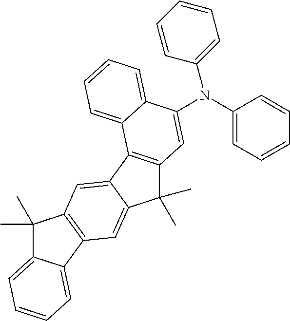 |
 |
 |
 |
 |
 |
 |
 |
 |
 |
 |
 |
 |
 |
 |
 |
 |
 |
 |
 |
 |
 |
 |
 |
 |
 |
 |
 |
 |
 |
 |
 |
 |
 |
 |
 |
 |
 |
 |
 |
 |
 |
 |
 |
 |
 |
 |
 |
 |
 |
 |
 |
 |
 |
 |
 |
 |
 |
 |
 |
 |
 |
 |


| TABLE 1 |
| Structure of the OLEDs |
| HTL | IL | EBL | EML | HBL | ETL | |
| Ex. | Thickness | Thickness | Thickness | Thickness | Thickness | Thickness |
| V1 | SpA1 | HATCN | HTM1 | IC1:TEG1 (90%:10%) | ST1 | ST1:LiQ (50%:50%) 30 nm |
| 70 nm | 5 nm | 90 nm | 30 nm | 10 nm | ||
| V2 | SpA1 | HATCN | HTM2 | IC1:TEG1 (90%:10%) | ST1 | ST1:LiQ (50%:50%) 30 nm |
| 70 nm | 5 nm | 90 nm | 30 nm | 10 nm | ||
| E1 | SpA1 | HATCN | HTM3 | IC1:TEG1 (90%:10%) | ST1 | ST1:LiQ (50%:50%) 30 nm |
| 70 nm | 5 nm | 90 nm | 30 nm | 10 nm | ||
| E2 | SpA1 | HATCN | HTM4 | IC1:TEG1 (90%:10%) | ST1 | ST1:LiQ (50%:50%) 30 nm |
| 70 nm | 5 nm | 90 nm | 30 nm | 10 nm | ||
| E3 | SpA1 | HATCN | BPA1 | ST1:HTM3:TEG1 | — | ST1:LiQ (50%:50%) |
| 70 nm | 5 nm | 90 nm | (30%:60%:10%) 30 nm | 30 nm | ||
| E4 | SpA1 | HATCN | BPA1 | ST1:HTM4:TEG1 | — | ST1:LiQ (50%:50%) |
| 70 nm | 5 nm | 90 nm | (30%:60%:10%) 30 nm | 30 nm | ||
| E5 | SpA1 | HATCN | BPA1 | M2:TEG1 (90%:10%) | ST1 | ST1:LiQ (50%:50%) 30 nm |
| 70 nm | 5 nm | 90 nm | 30 nm | 10 nm | ||
| E6 | SpA1 | HATCN | BPA1 | M3:TEG1 (90%:10%) | ST1 | ST1:LiQ (50%:50%) 30 nm |
| 70 nm | 5 nm | 90 nm | 30 nm | 10 nm | ||
| E7 | SpA1 | HATCN | BPA1 | M3:TEG1 (90%:10%) | — | ST1:LiQ (50%:50%) 30 nm |
| 70 nm | 5 nm | 90 nm | 30 nm | |||
| E8 | SpA1 | HATCN | BPA1 | M4:TEG1 (90%:10%) | ST1 | ST1:LiQ (50%:50%) 30 nm |
| 70 nm | 5 nm | 90 nm | 30 nm | 10 nm | ||
| TABLE 2 |
| Data for the OLEDs |
| CIE x/y at | L0 | |||||||
| U1000 | CE1000 | PE1000 | EQE | 1000 | (cd/ | L1 | LT | |
| Ex. | (V) | (cd/A) | (lm/W) | 1000 | cd/m2 | m2) | % | (h) |
| V1 | 3.7 | 54 | 46 | 14.9% | 0.36/0.60 | 4000 | 80 | 45 |
| V2 | 3.9 | 48 | 39 | 13.4% | 0.36/0.60 | 4000 | 80 | 30 |
| E1 | 3.6 | 49 | 43 | 13.6% | 0.36/0.60 | 4000 | 80 | 360 |
| E2 | 3.8 | 56 | 46 | 15.4% | 0.36/0.60 | 4000 | 80 | 385 |
| E3 | 3.9 | 52 | 42 | 14.4% | 0.37/0.61 | 4000 | 80 | 460 |
| E4 | 3.8 | 54 | 45 | 15.1% | 0.37/0.61 | 4000 | 80 | 480 |
| E5 | 3.7 | 47 | 40 | 13.0% | 0.36/0.60 | 4000 | 80 | 340 |
| E6 | 3.4 | 54 | 50 | 15.5% | 0.37/0.59 | 4000 | 80 | 305 |
| E7 | 3.5 | 56 | 51 | 15.7% | 0.38/0.59 | 4000 | 80 | 280 |
| E8 | 3.5 | 53 | 47 | 14.8% | 0.36/0.60 | 4000 | 80 | 260 |
| TABLE 3 |
| Structural formulae of the materials for the OLEDs |
 |
 |
 |
 |
 |
 |
 |
 |
 |
 |
 |
 |
 |
 |
Claims (13)


Priority Applications (1)
| Application Number | Priority Date | Filing Date | Title |
|---|---|---|---|
| US15/386,119 US10749117B2 (en) | 2010-08-05 | 2016-12-21 | Materials for electronic devices |
Applications Claiming Priority (6)
| Application Number | Priority Date | Filing Date | Title |
|---|---|---|---|
| DE102010033548A DE102010033548A1 (en) | 2010-08-05 | 2010-08-05 | Materials for electronic devices |
| DE102010033548.7 | 2010-08-05 | ||
| DE102010033548 | 2010-08-05 | ||
| PCT/EP2011/003484 WO2012016630A1 (en) | 2010-08-05 | 2011-07-12 | Materials for electronic devices |
| US13/813,162 US9893297B2 (en) | 2010-08-05 | 2011-07-12 | Materials for electronic devices |
| US15/386,119 US10749117B2 (en) | 2010-08-05 | 2016-12-21 | Materials for electronic devices |
Related Parent Applications (2)
| Application Number | Title | Priority Date | Filing Date |
|---|---|---|---|
| US13/813,162 Division US9893297B2 (en) | 2010-08-05 | 2011-07-12 | Materials for electronic devices |
| PCT/EP2011/003484 Division WO2012016630A1 (en) | 2010-08-05 | 2011-07-12 | Materials for electronic devices |
Publications (2)
| Publication Number | Publication Date |
|---|---|
| US20170104165A1 US20170104165A1 (en) | 2017-04-13 |
| US10749117B2 true US10749117B2 (en) | 2020-08-18 |
Family
ID=44677825
Family Applications (2)
| Application Number | Title | Priority Date | Filing Date |
|---|---|---|---|
| US13/813,162 Active 2033-12-09 US9893297B2 (en) | 2010-08-05 | 2011-07-12 | Materials for electronic devices |
| US15/386,119 Active 2032-09-24 US10749117B2 (en) | 2010-08-05 | 2016-12-21 | Materials for electronic devices |
Family Applications Before (1)
| Application Number | Title | Priority Date | Filing Date |
|---|---|---|---|
| US13/813,162 Active 2033-12-09 US9893297B2 (en) | 2010-08-05 | 2011-07-12 | Materials for electronic devices |
Country Status (4)
| Country | Link |
|---|---|
| US (2) | US9893297B2 (en) |
| JP (1) | JP5940534B2 (en) |
| DE (2) | DE102010033548A1 (en) |
| WO (1) | WO2012016630A1 (en) |
Families Citing this family (28)
| Publication number | Priority date | Publication date | Assignee | Title |
|---|---|---|---|---|
| TWI558707B (en) * | 2010-09-13 | 2016-11-21 | Nippon Steel Chemical Co | Nitrogen-containing aromatic compounds, organic semiconductor materials and organic electronic devices |
| US8766249B2 (en) * | 2010-10-13 | 2014-07-01 | Nippon Steel & Sumikin Chemical Co., Ltd. | Nitrogenated aromatic compound, organic semiconductor material, and organic electronic device |
| DE102011011539A1 (en) | 2011-02-17 | 2012-08-23 | Merck Patent Gmbh | Connections for electronic devices |
| JP5741373B2 (en) * | 2011-10-25 | 2015-07-01 | コニカミノルタ株式会社 | ORGANIC ELECTROLUMINESCENT ELEMENT MATERIAL, ORGANIC ELECTROLUMINESCENT ELEMENT, DISPLAY DEVICE, AND LIGHTING DEVICE |
| CN104039773B (en) * | 2011-11-11 | 2016-08-24 | 东曹株式会社 | There is the cyclic azine compound of nitrogenous contracting polycyclic aromatic group and manufacture method thereof and with this cyclic azine compound organic electroluminescent device as constituent |
| JP5998841B2 (en) * | 2012-10-22 | 2016-09-28 | 東ソー株式会社 | Amine compound, production method and use thereof, production intermediate and production intermediate production method |
| KR20140086880A (en) * | 2012-12-28 | 2014-07-08 | 주식회사 동진쎄미켐 | Novel organic compound and organic electroluminescent device comprising same |
| WO2014104797A1 (en) * | 2012-12-28 | 2014-07-03 | 주식회사 동진쎄미켐 | Novel organic compound and organic light emitting device containing same |
| KR102245921B1 (en) * | 2013-05-28 | 2021-04-29 | 주식회사 동진쎄미켐 | Novel organic compound and organic electroluminescent device comprising same |
| WO2014193153A1 (en) * | 2013-05-28 | 2014-12-04 | 주식회사 동진쎄미켐 | Novel organic compound and organic light-emitting device comprising same |
| KR102208958B1 (en) | 2013-10-01 | 2021-01-28 | 삼성전자주식회사 | Condensed compound and organic light emitting diode including the same |
| WO2015076600A1 (en) * | 2013-11-20 | 2015-05-28 | 주식회사 동진쎄미켐 | Novel light emission compound and organic light emitting device comprising same |
| CN105765030B (en) * | 2013-11-20 | 2018-07-17 | 东进世美肯株式会社 | Novel light-emitting compound and organic illuminating element comprising it |
| KR20150058082A (en) * | 2013-11-20 | 2015-05-28 | 주식회사 동진쎄미켐 | Novel electroluminescent compound and organic electroluminescent device comprising same |
| WO2015076599A1 (en) * | 2013-11-20 | 2015-05-28 | 주식회사 동진쎄미켐 | Novel light emission compound and organic light emitting device comprising same |
| WO2015084032A1 (en) * | 2013-12-03 | 2015-06-11 | 주식회사 동진쎄미켐 | Novel hole injection and hole transport compound and organic light-emitting element comprising same |
| KR102394381B1 (en) * | 2013-12-03 | 2022-05-06 | 주식회사 동진쎄미켐 | Novel hole injecting· hole-transporting compound and organic electroluminescent device comprising same |
| KR102437956B1 (en) * | 2014-05-16 | 2022-09-01 | 주식회사 동진쎄미켐 | Novel compound and organic electroluminescent device comprising same |
| WO2015174791A1 (en) * | 2014-05-16 | 2015-11-19 | 주식회사 동진쎄미켐 | Novel compound and organic light-emitting element comprising same |
| JP6070756B2 (en) * | 2015-04-15 | 2017-02-01 | コニカミノルタ株式会社 | ORGANIC ELECTROLUMINESCENT ELEMENT MATERIAL, ORGANIC ELECTROLUMINESCENT ELEMENT, METHOD FOR PRODUCING ORGANIC ELECTROLUMINESCENT ELEMENT, DISPLAY DEVICE, AND LIGHTING DEVICE |
| JP6657895B2 (en) * | 2015-12-10 | 2020-03-04 | コニカミノルタ株式会社 | Organic electroluminescence element, display device and lighting device |
| KR102462420B1 (en) | 2017-12-06 | 2022-11-03 | 삼성디스플레이 주식회사 | Condensed-cyclic compound and organic light emitting device comprising the same |
| KR20200018752A (en) * | 2018-08-10 | 2020-02-20 | 삼성디스플레이 주식회사 | Organic electroluminescence device and condensed cyclic compound for organic electroluminescence device |
| CN111303174B (en) * | 2018-12-11 | 2023-08-22 | 北京鼎材科技有限公司 | Organic electroluminescent material and application thereof |
| TW202039481A (en) | 2018-12-21 | 2020-11-01 | 美商西建公司 | Thienopyridine inhibitors of ripk2 |
| KR102649286B1 (en) * | 2019-05-03 | 2024-03-19 | 덕산네오룩스 주식회사 | Compound for organic electronic element, organic electronic element using the same, and an electronic device thereof |
| KR102344801B1 (en) * | 2019-07-15 | 2021-12-29 | 덕산네오룩스 주식회사 | Compound for organic electronic element, organic electronic element using the same, and an electronic device thereof |
| KR20210023008A (en) * | 2019-08-21 | 2021-03-04 | 엘티소재주식회사 | Heterocyclic compound and organic light emitting device comprising same |
Citations (10)
| Publication number | Priority date | Publication date | Assignee | Title |
|---|---|---|---|---|
| WO1999045081A1 (en) | 1998-03-03 | 1999-09-10 | Gentex Corporation | Near infrared-absorbing electrochromic compounds and devices comprising same |
| JP2001508083A (en) | 1997-11-12 | 2001-06-19 | モンテル テクノロジー カンパニー ビーブイ | Catalysts for metallocene and olefin polymerization |
| US6710906B2 (en) * | 1999-12-03 | 2004-03-23 | Gentex Corporation | Controlled diffusion coefficient electrochromic materials for use in electrochromic mediums and associated electrochromic devices |
| JP2005199633A (en) | 2004-01-19 | 2005-07-28 | Mitsubishi Kagaku Sanshi Corp | Process for producing crosslinked ethylene-based resin pipe |
| JP2006081987A (en) | 2004-09-15 | 2006-03-30 | Green Seiju:Kk | Distilled water production system |
| JP2006219393A (en) | 2005-02-09 | 2006-08-24 | Canon Inc | Compound, light emitting device and image display device |
| WO2006122630A1 (en) | 2005-05-20 | 2006-11-23 | Merck Patent Gmbh | Compounds for organic electronic devices |
| WO2009063780A1 (en) | 2007-11-12 | 2009-05-22 | Mitsui Chemicals, Inc. | Organic transistor |
| JP2010040829A (en) | 2008-08-06 | 2010-02-18 | Konica Minolta Holdings Inc | Organic electroluminescent element, display device, and lighting system |
| WO2010046259A1 (en) * | 2008-10-21 | 2010-04-29 | Basf Se | Polycyclic compounds for electronic applications |
Family Cites Families (98)
| Publication number | Priority date | Publication date | Assignee | Title |
|---|---|---|---|---|
| US4539507A (en) | 1983-03-25 | 1985-09-03 | Eastman Kodak Company | Organic electroluminescent devices having improved power conversion efficiencies |
| DE4111878A1 (en) | 1991-04-11 | 1992-10-15 | Wacker Chemie Gmbh | LADDER POLYMERS WITH CONJUGATED DOUBLE BINDINGS |
| JP2951434B2 (en) * | 1991-04-18 | 1999-09-20 | 三菱製紙株式会社 | Electrophotographic photoreceptor |
| JPH04329547A (en) * | 1991-04-30 | 1992-11-18 | Mitsubishi Paper Mills Ltd | Electrophotographic sensitive body |
| US5151629A (en) | 1991-08-01 | 1992-09-29 | Eastman Kodak Company | Blue emitting internal junction organic electroluminescent device (I) |
| JPH061973A (en) | 1992-06-18 | 1994-01-11 | Konica Corp | Organic electroluminescent element |
| JPH07133483A (en) | 1993-11-09 | 1995-05-23 | Shinko Electric Ind Co Ltd | Organic luminescent material for el element and el element |
| EP0676461B1 (en) | 1994-04-07 | 2002-08-14 | Covion Organic Semiconductors GmbH | Spiro compounds and their application as electroluminescence materials |
| DE69511755T2 (en) | 1994-04-26 | 2000-01-13 | Tdk Corp | Phenylanthracene derivative and organic EL element |
| DE4436773A1 (en) | 1994-10-14 | 1996-04-18 | Hoechst Ag | Conjugated polymers with spirocenters and their use as electroluminescent materials |
| JP3865406B2 (en) | 1995-07-28 | 2007-01-10 | 住友化学株式会社 | 2,7-Aryl-9-substituted fluorene and 9-substituted fluorene oligomers and polymers |
| DE19614971A1 (en) | 1996-04-17 | 1997-10-23 | Hoechst Ag | Polymers with spiro atoms and their use as electroluminescent materials |
| DE19652261A1 (en) | 1996-12-16 | 1998-06-18 | Hoechst Ag | Aryl-substituted poly (p-arylenevinylenes), process for their preparation and their use in electroluminescent devices |
| US5935721A (en) | 1998-03-20 | 1999-08-10 | Eastman Kodak Company | Organic electroluminescent elements for stable electroluminescent |
| DE19846766A1 (en) | 1998-10-10 | 2000-04-20 | Aventis Res & Tech Gmbh & Co | A conjugated fluorene-based polymer useful as an organic semiconductor, electroluminescence material, and for display elements |
| JP4429438B2 (en) | 1999-01-19 | 2010-03-10 | 出光興産株式会社 | Amino compound and organic electroluminescence device using the same |
| US6166172A (en) | 1999-02-10 | 2000-12-26 | Carnegie Mellon University | Method of forming poly-(3-substituted) thiophenes |
| EP1729327B2 (en) | 1999-05-13 | 2022-08-10 | The Trustees Of Princeton University | Use of a phosphorescent iridium compound as emissive molecule in an organic light emitting device |
| KR100840637B1 (en) | 1999-12-01 | 2008-06-24 | 더 트러스티즈 오브 프린스턴 유니버시티 | Complexes of form l2mx as phosphorescent dopants for organic leds |
| TW532048B (en) | 2000-03-27 | 2003-05-11 | Idemitsu Kosan Co | Organic electroluminescence element |
| US20020121638A1 (en) | 2000-06-30 | 2002-09-05 | Vladimir Grushin | Electroluminescent iridium compounds with fluorinated phenylpyridines, phenylpyrimidines, and phenylquinolines and devices made with such compounds |
| EP1325671B1 (en) | 2000-08-11 | 2012-10-24 | The Trustees Of Princeton University | Organometallic compounds and emission-shifting organic electrophosphorescence |
| JP4154138B2 (en) | 2000-09-26 | 2008-09-24 | キヤノン株式会社 | Light emitting element, display device and metal coordination compound |
| JP4154139B2 (en) | 2000-09-26 | 2008-09-24 | キヤノン株式会社 | Light emitting element |
| JP4154140B2 (en) | 2000-09-26 | 2008-09-24 | キヤノン株式会社 | Metal coordination compounds |
| GB0104177D0 (en) | 2001-02-20 | 2001-04-11 | Isis Innovation | Aryl-aryl dendrimers |
| KR100939468B1 (en) | 2001-03-10 | 2010-01-29 | 메르크 파텐트 게엠베하 | Solutions and dispersions of organic semiconductors |
| DE10141624A1 (en) | 2001-08-24 | 2003-03-06 | Covion Organic Semiconductors | Solutions of polymeric semiconductors |
| DE10159946A1 (en) | 2001-12-06 | 2003-06-18 | Covion Organic Semiconductors | Process for the production of aryl-aryl coupled compounds |
| DE10207859A1 (en) | 2002-02-20 | 2003-09-04 | Univ Dresden Tech | Doped organic semiconductor material and process for its production |
| ITRM20020411A1 (en) | 2002-08-01 | 2004-02-02 | Univ Roma La Sapienza | SPIROBIFLUORENE DERIVATIVES, THEIR PREPARATION AND USE. |
| KR100924462B1 (en) | 2002-08-23 | 2009-11-03 | 이데미쓰 고산 가부시키가이샤 | Organic electroluminescence device and anthracene derivative |
| DE10249723A1 (en) | 2002-10-25 | 2004-05-06 | Covion Organic Semiconductors Gmbh | Conjugated polymers containing arylamine units, their preparation and use |
| GB0226010D0 (en) | 2002-11-08 | 2002-12-18 | Cambridge Display Tech Ltd | Polymers for use in organic electroluminescent devices |
| JP4287198B2 (en) | 2002-11-18 | 2009-07-01 | 出光興産株式会社 | Organic electroluminescence device |
| WO2004058911A2 (en) | 2002-12-23 | 2004-07-15 | Covion Organic Semiconductors Gmbh | Organic electroluminescent element |
| DE10304819A1 (en) | 2003-02-06 | 2004-08-19 | Covion Organic Semiconductors Gmbh | Carbazole-containing conjugated polymers and blends, their preparation and use |
| DE10310887A1 (en) | 2003-03-11 | 2004-09-30 | Covion Organic Semiconductors Gmbh | Matallkomplexe |
| JP4411851B2 (en) | 2003-03-19 | 2010-02-10 | コニカミノルタホールディングス株式会社 | Organic electroluminescence device |
| US7586006B2 (en) | 2003-04-10 | 2009-09-08 | Idemitsu Kosan Co., Ltd. | Aromatic amine derivative and organic electroluminescent element employing the same |
| EP2281861A3 (en) | 2003-04-15 | 2012-03-28 | Merck Patent GmbH | Mixture of organic emission-enabled semiconductors and matrix materials, use of same and electronic components containing same |
| EP2236579B1 (en) | 2003-04-23 | 2014-04-09 | Konica Minolta Holdings, Inc. | Organic electroluminescent element and display |
| TWI224473B (en) | 2003-06-03 | 2004-11-21 | Chin-Hsin Chen | Doped co-host emitter system in organic electroluminescent devices |
| EP1491568A1 (en) | 2003-06-23 | 2004-12-29 | Covion Organic Semiconductors GmbH | Semiconductive Polymers |
| DE10328627A1 (en) | 2003-06-26 | 2005-02-17 | Covion Organic Semiconductors Gmbh | New materials for electroluminescence |
| US8592614B2 (en) | 2003-07-07 | 2013-11-26 | Merck Patent Gmbh | Mixtures of organic emissive semiconductors and matrix materials, their use and electronic components comprising said materials |
| DE10333232A1 (en) | 2003-07-21 | 2007-10-11 | Merck Patent Gmbh | Organic electroluminescent element |
| DE10337346A1 (en) | 2003-08-12 | 2005-03-31 | Covion Organic Semiconductors Gmbh | Conjugated polymers containing dihydrophenanthrene units and their use |
| DE10338550A1 (en) | 2003-08-19 | 2005-03-31 | Basf Ag | Transition metal complexes with carbene ligands as emitters for organic light-emitting diodes (OLEDs) |
| CN1849314B (en) | 2003-09-12 | 2011-07-20 | 住友化学株式会社 | Dendrimer compound and organic luminescent element employing the same |
| DE10345572A1 (en) | 2003-09-29 | 2005-05-19 | Covion Organic Semiconductors Gmbh | metal complexes |
| US7795801B2 (en) | 2003-09-30 | 2010-09-14 | Konica Minolta Holdings, Inc. | Organic electroluminescent element, illuminator, display and compound |
| EP1675930B1 (en) | 2003-10-22 | 2018-05-30 | Merck Patent GmbH | New materials for electroluminescence and the utilization thereof |
| DE10357044A1 (en) | 2003-12-04 | 2005-07-14 | Novaled Gmbh | Process for doping organic semiconductors with quinonediimine derivatives |
| US7252893B2 (en) | 2004-02-17 | 2007-08-07 | Eastman Kodak Company | Anthracene derivative host having ranges of dopants |
| DE102004008304A1 (en) | 2004-02-20 | 2005-09-08 | Covion Organic Semiconductors Gmbh | Organic electronic devices |
| US7326371B2 (en) | 2004-03-25 | 2008-02-05 | Eastman Kodak Company | Electroluminescent device with anthracene derivative host |
| US7790890B2 (en) | 2004-03-31 | 2010-09-07 | Konica Minolta Holdings, Inc. | Organic electroluminescence element material, organic electroluminescence element, display device and illumination device |
| DE102004020298A1 (en) | 2004-04-26 | 2005-11-10 | Covion Organic Semiconductors Gmbh | Electroluminescent polymers and their use |
| DE102004023277A1 (en) | 2004-05-11 | 2005-12-01 | Covion Organic Semiconductors Gmbh | New material mixtures for electroluminescence |
| US7598388B2 (en) | 2004-05-18 | 2009-10-06 | The University Of Southern California | Carbene containing metal complexes as OLEDs |
| TWI327563B (en) | 2004-05-24 | 2010-07-21 | Au Optronics Corp | Anthracene compound and organic electroluminescent device including the anthracene compound |
| JP4862248B2 (en) | 2004-06-04 | 2012-01-25 | コニカミノルタホールディングス株式会社 | Organic electroluminescence element, lighting device and display device |
| DE102004031000A1 (en) | 2004-06-26 | 2006-01-12 | Covion Organic Semiconductors Gmbh | Organic electroluminescent devices |
| TW200613515A (en) | 2004-06-26 | 2006-05-01 | Merck Patent Gmbh | Compounds for organic electronic devices |
| DE102004032527A1 (en) | 2004-07-06 | 2006-02-02 | Covion Organic Semiconductors Gmbh | Electroluminescent polymers |
| ITRM20040352A1 (en) | 2004-07-15 | 2004-10-15 | Univ Roma La Sapienza | OLIGOMERIC DERIVATIVES OF SPIROBIFLUORENE, THEIR PREPARATION AND THEIR USE. |
| EP1655359A1 (en) | 2004-11-06 | 2006-05-10 | Covion Organic Semiconductors GmbH | Organic electroluminescent device |
| TW200639140A (en) | 2004-12-01 | 2006-11-16 | Merck Patent Gmbh | Compounds for organic electronic devices |
| EP1669386A1 (en) | 2004-12-06 | 2006-06-14 | Covion Organic Semiconductors GmbH | Conjugated polymers, representation thereof, and use |
| JP4263700B2 (en) | 2005-03-15 | 2009-05-13 | 出光興産株式会社 | Aromatic amine derivative and organic electroluminescence device using the same |
| US20090066225A1 (en) | 2005-03-18 | 2009-03-12 | Idemitsu Kosan Co., Ltd. | Aromatic amine derivative and organic electroluminescence device utilizing the same |
| JP5242380B2 (en) | 2005-05-03 | 2013-07-24 | メルク パテント ゲーエムベーハー | Organic electroluminescence device |
| BRPI0613785A2 (en) | 2005-07-08 | 2011-02-01 | Unilever Nv | starch-containing food product, process for preparing intact starch-containing plant cells and process for preparing starch-containing food product |
| DE102005037734B4 (en) | 2005-08-10 | 2018-02-08 | Merck Patent Gmbh | Electroluminescent polymers, their use and bifunctional monomeric compounds |
| US20070092755A1 (en) | 2005-10-26 | 2007-04-26 | Eastman Kodak Company | Organic element for low voltage electroluminescent devices |
| JP4593631B2 (en) | 2005-12-01 | 2010-12-08 | 新日鐵化学株式会社 | Compound for organic electroluminescence device and organic electroluminescence device |
| DE102005058543A1 (en) | 2005-12-08 | 2007-06-14 | Merck Patent Gmbh | Organic electroluminescent devices |
| DE102005058557A1 (en) | 2005-12-08 | 2007-06-14 | Merck Patent Gmbh | Organic electroluminescent device |
| DE102005060473A1 (en) | 2005-12-17 | 2007-06-28 | Merck Patent Gmbh | Conjugated polymers, their preparation and use |
| DE102006015183A1 (en) | 2006-04-01 | 2007-10-04 | Merck Patent Gmbh | New benzocycloheptene compound useful in organic electronic devices e.g. organic electroluminescent device, polymer electroluminescent device and organic field-effect-transistors |
| DE102006025777A1 (en) | 2006-05-31 | 2007-12-06 | Merck Patent Gmbh | New materials for organic electroluminescent devices |
| DE102006025846A1 (en) | 2006-06-02 | 2007-12-06 | Merck Patent Gmbh | New materials for organic electroluminescent devices |
| DE102006031990A1 (en) | 2006-07-11 | 2008-01-17 | Merck Patent Gmbh | New materials for organic electroluminescent devices |
| FR2904474B1 (en) * | 2006-07-27 | 2008-10-24 | Commissariat Energie Atomique | WHITE-EMITTING ORGANIC ELECTROLUMINESCENT DIODES BASED ON PHOSPHOL-DERIVED MOLECULES |
| WO2008056746A1 (en) | 2006-11-09 | 2008-05-15 | Nippon Steel Chemical Co., Ltd. | Compound for organic electroluminescent device and organic electroluminescent device |
| DE102007002714A1 (en) | 2007-01-18 | 2008-07-31 | Merck Patent Gmbh | New materials for organic electroluminescent devices |
| DE102007024850A1 (en) | 2007-05-29 | 2008-12-04 | Merck Patent Gmbh | New materials for organic electroluminescent devices |
| DE102007053771A1 (en) | 2007-11-12 | 2009-05-14 | Merck Patent Gmbh | Organic electroluminescent devices |
| DE102008033943A1 (en) | 2008-07-18 | 2010-01-21 | Merck Patent Gmbh | New materials for organic electroluminescent devices |
| DE102008035413A1 (en) | 2008-07-29 | 2010-02-04 | Merck Patent Gmbh | Connections for organic electronic devices |
| DE102008036982A1 (en) | 2008-08-08 | 2010-02-11 | Merck Patent Gmbh | Organic electroluminescent device |
| CN102076813B (en) | 2008-11-11 | 2016-05-18 | 默克专利有限公司 | Organic electroluminescence device |
| DE102008056688A1 (en) | 2008-11-11 | 2010-05-12 | Merck Patent Gmbh | Materials for organic electroluminescent devices |
| DE102009023155A1 (en) | 2009-05-29 | 2010-12-02 | Merck Patent Gmbh | Materials for organic electroluminescent devices |
| DE102009031021A1 (en) | 2009-06-30 | 2011-01-05 | Merck Patent Gmbh | Materials for organic electroluminescent devices |
| DE102010005697A1 (en) | 2010-01-25 | 2011-07-28 | Merck Patent GmbH, 64293 | Connections for electronic devices |
| DE102010014933A1 (en) | 2010-04-14 | 2011-10-20 | Merck Patent Gmbh | Materials for electronic devices |
-
2010
- 2010-08-05 DE DE102010033548A patent/DE102010033548A1/en not_active Withdrawn
-
2011
- 2011-07-12 US US13/813,162 patent/US9893297B2/en active Active
- 2011-07-12 WO PCT/EP2011/003484 patent/WO2012016630A1/en active Application Filing
- 2011-07-12 DE DE112011102619T patent/DE112011102619A5/en not_active Ceased
- 2011-07-12 JP JP2013522121A patent/JP5940534B2/en not_active Expired - Fee Related
-
2016
- 2016-12-21 US US15/386,119 patent/US10749117B2/en active Active
Patent Citations (15)
| Publication number | Priority date | Publication date | Assignee | Title |
|---|---|---|---|---|
| JP2001508083A (en) | 1997-11-12 | 2001-06-19 | モンテル テクノロジー カンパニー ビーブイ | Catalysts for metallocene and olefin polymerization |
| US6451724B1 (en) | 1997-11-12 | 2002-09-17 | Basell Technology Company Bv | Metallocenes and catalysts for olefin-polymerisation |
| US6193912B1 (en) | 1998-03-03 | 2001-02-27 | Gentex Corporation | Near infrared-absorbing electrochromic compounds and devices comprising same |
| WO1999045081A1 (en) | 1998-03-03 | 1999-09-10 | Gentex Corporation | Near infrared-absorbing electrochromic compounds and devices comprising same |
| US6710906B2 (en) * | 1999-12-03 | 2004-03-23 | Gentex Corporation | Controlled diffusion coefficient electrochromic materials for use in electrochromic mediums and associated electrochromic devices |
| JP4329547B2 (en) | 2004-01-19 | 2009-09-09 | 三菱樹脂株式会社 | Method for producing cross-linked ethylene resin tube |
| JP2005199633A (en) | 2004-01-19 | 2005-07-28 | Mitsubishi Kagaku Sanshi Corp | Process for producing crosslinked ethylene-based resin pipe |
| JP2006081987A (en) | 2004-09-15 | 2006-03-30 | Green Seiju:Kk | Distilled water production system |
| JP4319958B2 (en) | 2004-09-15 | 2009-08-26 | 株式会社グリーンセイジュ | Distilled water production system |
| JP2006219393A (en) | 2005-02-09 | 2006-08-24 | Canon Inc | Compound, light emitting device and image display device |
| WO2006122630A1 (en) | 2005-05-20 | 2006-11-23 | Merck Patent Gmbh | Compounds for organic electronic devices |
| US20080220285A1 (en) | 2005-05-20 | 2008-09-11 | Merck Patent Gmbh | Novel Materials for Organic Electroluminescent Devices |
| WO2009063780A1 (en) | 2007-11-12 | 2009-05-22 | Mitsui Chemicals, Inc. | Organic transistor |
| JP2010040829A (en) | 2008-08-06 | 2010-02-18 | Konica Minolta Holdings Inc | Organic electroluminescent element, display device, and lighting system |
| WO2010046259A1 (en) * | 2008-10-21 | 2010-04-29 | Basf Se | Polycyclic compounds for electronic applications |
Non-Patent Citations (11)
Also Published As
| Publication number | Publication date |
|---|---|
| WO2012016630A1 (en) | 2012-02-09 |
| JP5940534B2 (en) | 2016-06-29 |
| US20170104165A1 (en) | 2017-04-13 |
| US9893297B2 (en) | 2018-02-13 |
| JP2013535476A (en) | 2013-09-12 |
| DE102010033548A1 (en) | 2012-02-09 |
| US20130126792A1 (en) | 2013-05-23 |
| DE112011102619A5 (en) | 2013-05-16 |
Similar Documents
| Publication | Publication Date | Title |
|---|---|---|
| US10749117B2 (en) | Materials for electronic devices | |
| US11641775B2 (en) | Compounds and organic electronic devices | |
| US11258018B2 (en) | Compounds and organic electronic devices | |
| US10135003B2 (en) | Materials for electronic devices | |
| US9139582B2 (en) | Organic electroluminescent devices | |
| US10056549B2 (en) | Compounds for electronic devices | |
| US9780311B2 (en) | Compounds for electronic devices | |
| US10008672B2 (en) | Compounds for electronic devices | |
| US9334260B2 (en) | Materials for electronic devices | |
| US9090590B2 (en) | Organic compounds for electroluminescent devices | |
| US20130012700A1 (en) | Materials for organic electroluminescent devices | |
| US20120202997A1 (en) | Materials for organic electroluminescent devices | |
| US9812643B2 (en) | Materials for electronic devices | |
| US20130193382A1 (en) | Compounds for electronic devices | |
| US9876171B2 (en) | Materials for electronic devices | |
| US10351557B2 (en) | Compounds for electronic devices | |
| US20150340627A1 (en) | Materials for electronic devices | |
| US10065959B2 (en) | Electronic device | |
| US9768385B2 (en) | Compounds for electronic devices | |
| US9593087B2 (en) | Materials for organic electroluminescent devices |
Legal Events
| Date | Code | Title | Description |
|---|---|---|---|
| AS | Assignment |
Owner name: MERCK PATENT GMBH, GERMANY Free format text: ASSIGNMENT OF ASSIGNORS INTEREST;ASSIGNORS:MARTYNOVA, IRINA;FRANZ, ADAM W.;PFLUMM, CHRISTOF;AND OTHERS;SIGNING DATES FROM 20170301 TO 20170315;REEL/FRAME:041638/0388 |
|
| STPP | Information on status: patent application and granting procedure in general |
Free format text: NON FINAL ACTION MAILED |
|
| STPP | Information on status: patent application and granting procedure in general |
Free format text: RESPONSE TO NON-FINAL OFFICE ACTION ENTERED AND FORWARDED TO EXAMINER |
|
| STPP | Information on status: patent application and granting procedure in general |
Free format text: FINAL REJECTION MAILED |
|
| STPP | Information on status: patent application and granting procedure in general |
Free format text: ADVISORY ACTION MAILED |
|
| STPP | Information on status: patent application and granting procedure in general |
Free format text: DOCKETED NEW CASE - READY FOR EXAMINATION |
|
| STPP | Information on status: patent application and granting procedure in general |
Free format text: AWAITING TC RESP., ISSUE FEE NOT PAID |
|
| STCF | Information on status: patent grant |
Free format text: PATENTED CASE |
|
| MAFP | Maintenance fee payment |
Free format text: PAYMENT OF MAINTENANCE FEE, 4TH YEAR, LARGE ENTITY (ORIGINAL EVENT CODE: M1551); ENTITY STATUS OF PATENT OWNER: LARGE ENTITY Year of fee payment: 4 |