US10700490B2 - Pseudo-balanced driver - Google Patents
Pseudo-balanced driver Download PDFInfo
- Publication number
- US10700490B2 US10700490B2 US16/312,738 US201716312738A US10700490B2 US 10700490 B2 US10700490 B2 US 10700490B2 US 201716312738 A US201716312738 A US 201716312738A US 10700490 B2 US10700490 B2 US 10700490B2
- Authority
- US
- United States
- Prior art keywords
- voltage
- node
- current
- laser
- modulator
- Prior art date
- Legal status (The legal status is an assumption and is not a legal conclusion. Google has not performed a legal analysis and makes no representation as to the accuracy of the status listed.)
- Active, expires
Links
Images




Classifications
-
- H—ELECTRICITY
- H01—ELECTRIC ELEMENTS
- H01S—DEVICES USING THE PROCESS OF LIGHT AMPLIFICATION BY STIMULATED EMISSION OF RADIATION [LASER] TO AMPLIFY OR GENERATE LIGHT; DEVICES USING STIMULATED EMISSION OF ELECTROMAGNETIC RADIATION IN WAVE RANGES OTHER THAN OPTICAL
- H01S5/00—Semiconductor lasers
- H01S5/04—Processes or apparatus for excitation, e.g. pumping, e.g. by electron beams
- H01S5/042—Electrical excitation ; Circuits therefor
-
- H—ELECTRICITY
- H01—ELECTRIC ELEMENTS
- H01S—DEVICES USING THE PROCESS OF LIGHT AMPLIFICATION BY STIMULATED EMISSION OF RADIATION [LASER] TO AMPLIFY OR GENERATE LIGHT; DEVICES USING STIMULATED EMISSION OF ELECTROMAGNETIC RADIATION IN WAVE RANGES OTHER THAN OPTICAL
- H01S5/00—Semiconductor lasers
- H01S5/04—Processes or apparatus for excitation, e.g. pumping, e.g. by electron beams
- H01S5/042—Electrical excitation ; Circuits therefor
- H01S5/0427—Electrical excitation ; Circuits therefor for applying modulation to the laser
-
- H—ELECTRICITY
- H01—ELECTRIC ELEMENTS
- H01S—DEVICES USING THE PROCESS OF LIGHT AMPLIFICATION BY STIMULATED EMISSION OF RADIATION [LASER] TO AMPLIFY OR GENERATE LIGHT; DEVICES USING STIMULATED EMISSION OF ELECTROMAGNETIC RADIATION IN WAVE RANGES OTHER THAN OPTICAL
- H01S3/00—Lasers, i.e. devices using stimulated emission of electromagnetic radiation in the infrared, visible or ultraviolet wave range
- H01S3/005—Optical devices external to the laser cavity, specially adapted for lasers, e.g. for homogenisation of the beam or for manipulating laser pulses, e.g. pulse shaping
- H01S3/0085—Modulating the output, i.e. the laser beam is modulated outside the laser cavity
-
- H—ELECTRICITY
- H01—ELECTRIC ELEMENTS
- H01S—DEVICES USING THE PROCESS OF LIGHT AMPLIFICATION BY STIMULATED EMISSION OF RADIATION [LASER] TO AMPLIFY OR GENERATE LIGHT; DEVICES USING STIMULATED EMISSION OF ELECTROMAGNETIC RADIATION IN WAVE RANGES OTHER THAN OPTICAL
- H01S5/00—Semiconductor lasers
- H01S5/005—Optical components external to the laser cavity, specially adapted therefor, e.g. for homogenisation or merging of the beams or for manipulating laser pulses, e.g. pulse shaping
- H01S5/0085—Optical components external to the laser cavity, specially adapted therefor, e.g. for homogenisation or merging of the beams or for manipulating laser pulses, e.g. pulse shaping for modulating the output, i.e. the laser beam is modulated outside the laser cavity
-
- H—ELECTRICITY
- H01—ELECTRIC ELEMENTS
- H01S—DEVICES USING THE PROCESS OF LIGHT AMPLIFICATION BY STIMULATED EMISSION OF RADIATION [LASER] TO AMPLIFY OR GENERATE LIGHT; DEVICES USING STIMULATED EMISSION OF ELECTROMAGNETIC RADIATION IN WAVE RANGES OTHER THAN OPTICAL
- H01S5/00—Semiconductor lasers
- H01S5/04—Processes or apparatus for excitation, e.g. pumping, e.g. by electron beams
- H01S5/042—Electrical excitation ; Circuits therefor
- H01S5/0428—Electrical excitation ; Circuits therefor for applying pulses to the laser
Definitions
- the invention relates to the field of drivers for lasers or modulators. More specifically it relates to the field of high-speed drivers for cathode-driven lasers or of high-speed drivers for modulators.
- a cathode-drive laser driver can be represented in a simplified matter as a current source which can drive a current through a laser.
- FIG. 1 shows schematically such a back terminated laser driver.
- High-speed cathode-drive laser drivers are typically implemented with a back termination resistor to move the dominant pole to higher frequencies.
- the anode voltage of the laser affects the average laser current and needs to be set at a specific value in order to minimize this impact.
- the back termination resistor R t (resistor 11 in FIG. 1 ) not only reduces the drive efficiency (m) to the laser, but also introduces a DC current path between the supply voltage node of the driver Vdd 1 (the voltage at node 121 in FIG. 1 ) and the anode voltage node of the laser 195 Vdd 2 (the voltage at node 191 in FIG. 1 ).
- the current through the laser only depends on the current from the driver but as there are two supply voltages there is an extra current path between the supply voltage node of the driver Vdd 1 and the anode voltage node of the laser Vdd 2 .
- This extra current depends on the difference between the supply voltages Vdd 1 and Vdd 2 .
- the current can be a negative or a positive current, of which the value is hard to predict or control because of the dependence on R t and on the series resistance of the laser R 1 (the laser can be modelled as a voltage source Vlth and a resistor RI at DC), hence a constraint on the anode voltage arises that minimizes the extra undesired current through the laser.
- the graph in FIG. 1 shows the optical power as function of the laser current I l .
- the graph shows the relation between the modulation current I m , the bias current I b and the average laser current ⁇ l .
- a back-terminated driver for driving a cathode-driven laser or for driving a modulator.
- the driver comprises:
- the replica voltage generated by the replica block allows equalizing DC voltages in the driver by using the pre-defined voltage. Thereby undesired currents in the switch block can be avoided.
- a driver is used for driving a laser and when the pre-defined voltage is selected such that it approximates the threshold voltage drop of the laser, an undesired DC current flow between the voltage supply node of the laser (Vdd 2 ) and the voltage supply node of the driver (Vdd 1 ) is prevented.
- a voltage converter in accordance with embodiments of the present invention it achieves low-power operation by removing the anode voltage constraint.
- Vdd 2 equal to Vdd 1 leveraging an electro-optic laser transmitter utilizing a single supply voltage.
- This can greatly simplify the external power supply modules accompanied by a decrease in power dissipation. Power dissipation is further reduced because the drive current can maintain its state regardless of the value of the anode voltage Vdd 2 , resulting in a minimum required drive current when targeting a certain laser current.
- the voltage converter comprises a voltage converter block comprising a first input node, a second input node, said voltage supply node and said output port, wherein said output port is connected to the common node of the switch block, wherein the voltage replica block comprises said input port and an output port connected to the first input node of the voltage converter block and wherein the voltage converter block is adapted for equalizing the DC voltage at the first input node with the DC voltage at the second input node by controlling the output port.
- the second input node of the voltage converter block is connected with the common node of the switch block when the driver is adapted for driving a cathode-driven laser.
- the second input node of the voltage converter block is adapted for obtaining the average voltage at the current node of the switch block when the driver is adapted for driving a modulator.
- the balancer is adapted for equalizing the voltages of the current node and of the second node of the switch block.
- the voltage converter block comprises a transistor and an operational amplifier, the operational amplifier comprising a first input node, a second input node, and an output.
- the operational amplifier comprising a first input node, a second input node, and an output.
- the voltage converter block comprises an operational amplifier, a current source and a common-mode resistor,
- the voltage drop between the voltage supply node and the common node can be controlled by controlling the current through a current source of the voltage converter.
- the voltage converter block is a switch-mode power supply.
- the balancer comprises a first and a second input terminal and an output terminal adapted to source current, wherein the first input terminal is connected to current node of the switch block, and wherein the second input terminal is connected to second node of the switch block, and wherein the balancer is adapted to source a current via the output terminal, based on the voltage difference between the first input terminal and the second input terminal, to make the load of the switch block symmetrical.
- the voltage replica block is adaptable to a plurality of pre-defined voltages.
- drivers in accordance with at least some embodiments of the present invention can be used to drive a different laser with a different laser threshold voltage drop.
- the voltage replica block may be programmable to a plurality of pre-defined voltages.
- the voltage replica block may comprise an input port which allows to modulate the pre-defined voltage.
- the voltage replica block may comprise a programmable parameter or appropriate temperature dependence to change the copy of the threshold voltage drop. It is thereby an advantage that a better match between the threshold voltage drop of the laser and the voltage over the voltage replica block can be achieved.
- embodiments of the present invention relate to an opto-electronics transmitter comprising a back-terminated driver according embodiments of the present invention and a cathode-driven laser, wherein the pre-defined voltage of the voltage replica block approximates the threshold voltage drop of the laser.
- the laser 195 is connected between the voltage supply node 191 and the current node 119 with its anode towards the voltage supply node and its cathode towards the current node.
- the laser supply voltage can be smaller than the sum of the driver supply voltage and the lasers threshold voltage. It is an advantage of embodiments of the present invention that opto-electronics laser transmitters according to the present invention can be operated using a single supply voltage. This simplifies the external power supply modules and results in a decrease in power dissipation. In addition, the drive current can maintain its state despite a change in anode voltage Vdd 2 , which would not be the case if the drive current would be adapted based on the monitored laser current.
- the opto-electronics transmitter comprises a driver according to embodiments of the present invention and a modulator, wherein the top terminal of the modulator is AC-coupled with the second node and wherein the bottom terminal of the modulator is connected with the current node of the switch block, wherein during operation the pre-defined voltage sets the bias voltage of the modulator.
- the voltage replica block can be used to bias a modulator.
- FIG. 1 shows schematically a back terminated cathode-drive laser driver, as known from prior art.
- FIG. 2 shows an opto-electronics transmitter comprising a driver which is driving a cathode-driven laser in accordance with embodiments of the present invention.
- FIG. 3 is a graph showing the forward voltage of a laser in function of the current through the laser.
- FIG. 4 shows a similar driver as in FIG. 2 wherein the switch block comprises a transistor pair in accordance with embodiments of the present invention.
- FIG. 6 shows a similar driver as in FIG. 2 wherein the balancer is an identical laser connected to the dummy branch of the differential pair, in accordance with embodiments of the present invention.
- FIG. 7 shows a similar driver as in FIG. 2 illustrating a possible implementation of the voltage converter block and of the balancer in accordance with embodiments of the present invention.
- FIG. 9 shows a programmable voltage replica block comprising current source with positive temperature coefficient, in accordance with an exemplary embodiment of the present invention.
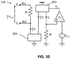
- FIG. 10 show a voltage replica block comprising a reference voltage that is isolated from the floating terminals of the voltage replica block.
- FIG. 11 show a voltage replica block using only the resistor ratio as a scale factor for Vref.
- FIG. 12 shows a laser/modulator driver in accordance with embodiments of the present invention wherein the driver is configured and connected with a cathode-driven laser for driving the laser.
- FIG. 14 shows an alternative configuration for driving a modulator in accordance with embodiments of the present invention.
- FIG. 15 and FIG. 16 schematically illustrate a driver which is connected with a modulator for single-endedly driving the modulator in accordance with embodiments of the present invention.
- the present invention relates to a back-terminated driver for driving a cathode-driven laser or a modulator.
- a laser may for example be a vertical-cavity surface emitting laser (VCSEL).
- VCSEL vertical-cavity surface emitting laser
- Drivers are comprising a voltage converter 120 .
- the voltage converter comprises a voltage replica block 124 and a voltage converter block 125 .
- the voltage converter 120 tracks the anode voltage and threshold voltage drop of a laser 195 by insertion of a voltage replica block 124 in the feedback loop that connects directly to the anode voltage node 191 .
- Purpose of the dual voltage tracking is to make the current I l through the laser 195 independent of variations on the lasers anode voltage and forward voltage.
- This configuration cancels the current flow I extra between the laser supply voltage node 191 (voltage Vdd 2 ) and the voltage supply node 121 (voltage Vdd 1 ) of the voltage converter. It allows lowering Vdd 2 smaller than Vdd 1 +Vlth wherein Vlth is the threshold voltage of the laser which is explained in FIG. 3 .
- Vlth is the threshold voltage of the laser which is explained in FIG. 3 .
- a balancer 130 is introduced in accordance with embodiments of the present invention.
- the voltage converter 120 is adapted to match the voltage at the common node 123 of the switch block 110 with the laser voltage Vzl. This allows lowering the power consumption of the driver.
- the advantage of the voltage converter in this configuration is that the extra current between Vdd 2 and Vdd 1 which is equal to
- V dd ⁇ ⁇ 2 - V dd ⁇ ⁇ 1 - V lth R t + ⁇ R l can be eliminated.
- Vdd 2 can vary under different operating conditions, it is desired that the voltage at the common node 123 of the switch block 110 follows these variations.
- the threshold voltage drop Vlth of the laser can also slightly change over temperature or from device to device. It is an advantage of embodiments of the present invention that also these changes can be tracked by the voltage replica block 124 .
- a voltage replica block is inserted between the Vdd 2 terminal 191 and the reference voltage terminal (the first input node 126 ) of the voltage converter block 125 .
- the voltage of the voltage replica block 124 voltage can be modified by providing a control input terminal 128 to cover a broad range of laser applications.
- the voltage replica block 124 comprises a dedicated control input terminal 128 . It is thereby an advantage that this allows interfacing the driver 100 to a broad range of lasers or provide calibration over temperature and after fabrication.
- the voltage converter block 125 can be implemented as a linear regulator or as a switched-mode power supply. An example of a linear regulator is illustrated in FIG. 7 .
- FIG. 3 is a graph showing the forward voltage of a laser in function of the current through the laser.
- the forward voltage refers to the total voltage drop over the laser. This also includes the resistive voltage drop from R l .
- Vlth the threshold voltage drop
- Vlth the voltage where the laser is starting to emit light. This voltage can be obtained by extracting it from the measured curve via a linear fitted model as shown in FIG. 3 .
- the graph shows the forward voltage in function of the laser current.
- the pre-defined voltage of the voltage replica block approximates the threshold voltage drop within a range of +/ ⁇ 5%, or even less.
- the voltage converter 120 is adapted for approximating the voltage at the common node 123 to the internal voltage of the laser Vzl (see FIG. 2 ).
- approximating the threshold voltage drop value means reaching it within a range of +/ ⁇ 5%.
- the voltage converter When driving a single ended load as in FIG. 2 , the voltage converter creates a node voltage Vz at the common node 123 that is lower than Vdd 1 (the voltage at the voltage supply node 121 ).
- Vdd 2 the laser supply voltage at node 191
- Vdd 1 the extra current between Vdd 2 and Vdd 1 becomes zero when Vdd 2 equals the sum of Vlth and Vz and thus allows lowering the anode voltage independent of Vdd 1 .
- the switch block 110 is a differential pair/driver that implements back termination resistors to target high-speed operation. Low-speed drivers avoiding these back termination resistors do not need the anode and forward voltage tracking loop as there is no undesired current flow between the two supply terminals.
- the transient current Iz through the voltage converter block 125 equals the transient current through the laser due to the asymmetric load and has a peak-to-peak swing of m ⁇ Im.
- the dynamics of the voltage converter block 125 are significantly slower than the differential driver 116 .
- the settling time of the converter block 125 will distort the eye diagram for patterns with long strings of Consecutive Identical Digits (CID) and results in increased intersymbol interference (ISI), noticeable in graph g of FIG. 2 .
- the ISI leads to a deteriorated eye height and eye width. This introduces a power penalty at the receiver side and makes the design of the Clock and Data Recovery (CDR) less robust.
- drivers according to the present invention are comprising a balancer to preserve the signal quality in the optical link by balancing the output stage.
- the output stage is the block that drives the laser. It may comprise the switch block 110 , the bias converter 150 , and the voltage converter 120 .
- the balancer minimizes the transient current through the voltage converter.
- the balancer 130 is a three-terminal control circuit block that senses the voltages of both branches of the differential pair at the current node 119 and at the second node 117 , and sources a current Id into the dummy branch to force the voltage at the second node 117 equal to the voltage at the current node 119 . Consequently the differential pair sees a symmetrical load at DC. Because it is impossible to perfectly match both impedances, the AC input impedance of the balancing circuit will differ from that of the laser, hence the name ‘pseudo-balanced’.
- Such a balancer 130 may comprise a dummy load connected to the switch block 110 adapted for enforcing the voltages at the current node 119 and at the second node 117 equal to each other, with the primary purpose to minimize the peak-to-peak switching current through voltage converter block 125 , thereby isolating the dynamics of the voltage converter block 125 from the drivers output current/voltage e and thus avoiding a deterioration in high-speed performance of the drivers output current/voltage e (visually explained by graphs f and g in FIG. 2 ; graph f showing the undistorted eye diagram and graph g showing the deteriorated eye diagram).
- balancer 130 can also improve high-speed performance in back terminated differential drivers without integrated voltage converter since an asymmetric load can result in non-linear effects such as a pulse-width distorted output current.
- the first transistor 112 and the second transistor 113 together with the first back termination resistor 114 and the second back termination resistor 115 constitute the differential pair switching a current I m to the single-ended laser.
- the modulation current source I m ( 140 ) can be replaced with a resistor to further lower Vtail and increase the headroom of the first and second transistor 112 , 113 if necessary.
- Current source I b ( 150 ) can also be omitted if no constant biasing of the laser is required.
- a common-mode feedback loop may be added in the preceding stage to set Vtail to increase the headroom of the first and second transistor 112 , 113 .
- the voltage at the common node 123 may be equalized with the voltage at the first input node 126 . In that case the voltage at the common node 123 will approximate the node voltage Vzl inside the laser. The voltage at the current node 119 equals Vzl minus a voltage drop across laser resistor RI.
- FIG. 5 shows an opto-electronics transmitter 800 comprising a driver 100 and a modulator 810 which can be differentially driven by the driver 100 .
- a modulator typically requires a modulation voltage Vs and a bias voltage to modulate the optical output power.
- the modulator can be single-ended DC-coupled to the driver, wherein the bottom terminal is connected to the current node 119 of the switch block 110 and the top terminal to the common node 123 of the switch block, effectively placing the modulator in parallel with resistor 114 . Without the presence of a voltage converter, node 123 corresponds to supply node 121 . This configuration would however result in an increased power consumption to generate the bias voltage.
- the power consumption is reduced by AC-coupling both nodes (the second node 117 and current node 119 of the switch block 110 ), but this requires two bias voltages and two bias tees. Multiple combinations of these configurations are possible but all suffer from previously mentioned drawbacks.
- the top terminal of the modulator 810 is AC-coupled to the second node 117 of the switch block 110 (e.g. over capacitor 830 ) while also connected to the modulator supply voltage node 191 and the bottom terminal of the modulator 810 is DC-coupled to the current node 119 of the switch block 110 .
- the top terminal is connected (through e.g. an inductor 820 ) to the supply voltage Vdd 2 (at modulator supply voltage node 191 ).
- the voltage converter 120 is adapted for equalizing DC voltages in the driver 110 during operation of the driver by using the pre-defined voltage.
- V l Vdd 2 ⁇ V y
- V y Vdd 2 ⁇ V lr
- the pre-defined voltage of the voltage replica block can approximate the bias voltage within a range of +/ ⁇ 1% or less depending on the gain and the voltage offset in the feedback loop of voltage converter 123 .
- this technique only requires one bias tee while still acquiring a precise control of the bias voltage. It is an advantage of this exemplary embodiment that no bias current is needed to generate a bias voltage thereby saving static power.
- a balancer 130 is connected to the switch block 110 .
- the modulator 810 such as an electroabsorption modulator
- the graph in FIG. 5 shows the output power of the modulator in an arbitrary function of the applied voltage. It shows the bias voltage Vlr and a modulation voltage Vs.
- FIG. 6 shows a driver in accordance with embodiments of the present invention wherein the balancer is an identical laser connected to the dummy branch of the differential pair.
- the balancer is an identical laser connected to the dummy branch of the differential pair.
- the base current Ib is drawn.
- current source 140 the modulation current Im is drawn.
- the same signal levels apply as for FIG. 2 , except for the base current of signal d that now equals m′ ⁇ Ib. Also the same eye diagram can be obtained, although in a less efficient way since an extra laser is necessary of which the optical output is not used.
- the driver 100 is balanced by applying a dummy load to the left branch of the transistor pair 112 , 113 .
- the dummy load i.e. the balancer 130
- the balancer moreover comprises an operational amplifier 1040 and a transistor 1050 .
- the first and second input terminal 131 , 132 are the inputs of the operational amplifier.
- the output of the operational amplifier is connected with the gate of the transistor 1050 .
- the operational amplifier 1040 and the transistor 1050 are configured in a feedback loop so as to equalize the voltage of the current node 119 and the voltage of the second node 117 of the switch block.
- the input transistors of the balancing amplifier 1040 are designed small in area in order to limit the added parasitic capacitance at output node Vy (the current node 119 ).
- reducing the transistor size enlarges the variance over process corners of the offset voltage at the inputs of amplifier 1040 .
- This imposes a slight imbalance between the two branches of the differential pair which translates into a higher transient current through the voltage converter block 125 .
- the parasitic capacitance introduced by the bias current source Ib and the bond pad dominate the input capacitance of amplifier 1040 .
- the input transistors of the amplifier 1040 can still be dimensioned small if the undesired input offset voltage is trimmed or calibrated post-production.
- the voltage converter block 125 in the example of FIG. 7 is a linear voltage regulator. It comprises an operational amplifier 1010 and a transistor 1020 .
- the voltage replica block 124 is connected with the first input of the operational amplifier 126 .
- the second input 127 of the operational amplifier 1010 is connected with the common node 123 of the switch block 110 .
- the output of the operational amplifier 1010 is connected with the gate of the transistor 1020 of the voltage converter block 125 .
- the transistor 1020 of the voltage converter block 125 is connected to the voltage supply node 121 on one side and to the common node 123 of the switch block 110 on the other side.
- the transistor 1020 can be replaced with a current source controlled by the operational amplifier 1010 , creating a voltage drop across a common-mode resistor connected between Vdd 1 (voltage supply node 121 ) and Vz (common node 123 ).
- the converter block 125 may also be a switched-mode power supply.
- the transistors present in a driver can be MOSFET and/or BJT depending on technology and available headroom.
- Multiple differential pairs can connect to nodes Vx ( 117 ) and Vy ( 119 ) to enable feed-forward equalization topologies or multi-level modulation.
- FIG. 8 shows a voltage replica block 124 in accordance with an exemplary embodiment of the present invention.
- the input 851 and the output 852 of the voltage replica block are floating terminals over which a voltage drop is created.
- the voltage drop can be made programmable and/or follow a certain temperature dependence.
- a possible implementation is a programmable Vbe-multiplier using bipolar junction transistors as shown in FIG. 8 .
- the voltage drop of the replica circuit equals Vce (the collector-emitter voltage) and its expression is stated below. Assuming that the current gain factor ⁇ of the transistor Q 0 is infinite (no current is flowing into the base of the transistor), Vce solely depends on the base-emitter voltage of the transistor Vbe and the resistor ratio. With this topology, Vce is lower bounded to Vbe and upper bounded to the breakdown voltage of transistor Q 0 .
- the voltage drop Vce can be made programmable by inserting switches in series with resistors R 0 to R N-1 . controlled with bits b 0 to b N-1 . These bits can be derived from a lookup table (LUT) that e.g. relates the bit word to the ambient temperature to track the lasers temperature dependence.
- LUT lookup table
- the LUT can also store bit words related to types of lasers with a different threshold voltage.
- the lasers temperature dependence can also be tracked by the intrinsic characteristics of the replica circuit itself.
- Bipolar junction transistors are characterized by a Vbe that has a temperature coefficient (TC) of approximately ⁇ 2 mV/K. This makes the TC of the Vbe multiplier equal to (1+Ra/Rb)*( ⁇ 2 mV/K).
- This TC can be altered by using a reference current source Iref that has a positive or negative TC since Vbe also depends on the current that flows through the transistor.
- FIG. 9 shows a programmable voltage replica block 124 , more specifically a programmable Vbe multiplier, in accordance with embodiments of the present invention.
- the current source is in this case a current source with a positive TC. This current source is also referred to as a proportional to absolute temperate (PTAT) current source.
- Iref can be expressed as:
- the reference voltage Vbe of the Vbe multiplier is sensitive to process variations, although much less than the gate-source voltage of a FET used in a Vgs multiplier, and perhaps can have a TC that does not match with the TC of the laser.
- the voltage replica circuit in FIG. 10 solves this issue by utilizing voltage-to-current conversions in a feedback loop.
- Amplifier A 1 drives control terminal Vg of first current mirror 853 until the voltage across resistor R 1 equals the stable reference voltage Vref, thus creating a current
- 1 Vref/R 1 .
- the first current mirror 853 scales 11 with a factor (mirror ratio) m/n, which can be a programmable parameter implemented with bit-controlled switches, while the second current mirror 854 sources the scaled current to a second resistor R 2 with a resistance equal to R 1 .
- the scale factor m/n can be distributed between the two current mirrors or included in the resistor ratio R 2 /R 1 and can be made smaller or larger than unity resulting in a Vce smaller or larger than Vref.
- the replica voltage Vce is not upper bounded by e.g. a breakdown voltage.
- the first and second current mirrors 853 , 854 can be avoided by using the topology shown in FIG. 11 .
- amplifier A 1 drives transistor M 1 until the voltage across the bottom resistor Rb (in FIG. 11 this corresponds with the combination of the parallel resistors in series with the bit controlled switches) equals Vref, thereby generating a current Vref/Rb.
- This current also flows through resistor Ra, creating a voltage drop equal to Vref*Ra/Rb and corresponds to the voltage replica Vce.
- resistor Rb can be made programmable by including bit-controlled switches in series with the bottom resistors.
- This topology will consume less area than the topology from FIG. 10 because the current mirrors 853 , 854 are absent.
- the voltage replica block illustrated in FIG. 10 is, however, less prone to process variations resulting in a scale factor which is less process sensitive.
- a driver 100 in accordance with embodiments of the present invention can provide an accurate and stable biasing of a load while simultaneously minimizing the power consumption. This can moreover be achieved at a high data rate (e.g. 40 Gb/s). It is moreover advantageous that only a minimum of bias tee/RLC interface elements are required for interfacing with the load (examples will be illustrated using FIG. 11 , FIG. 12 , and FIG. 13 ). In embodiments of the present invention such a driver may even lead to a single-supply voltage operation of the laser/modulator driver.
- the load is either a cathode-driven laser or either a modulator. In both cases, using a driver in accordance with embodiments of the present invention will result in a reduced power consumption.
- Power consumption is minimized by firstly reducing waste current through the load, e.g. between the voltage supply Vdd 2 at the load supply node 191 and the voltage supply of the driver Vdd 1 at the voltage supply node 121 , and secondly by making the drive current independent of the load supply voltage Vdd 2 , thereby simplifying the design of the preceding stage.
- FIGS. 12, 13, and 14 illustrate how a driver 100 , in accordance with embodiments of the present invention, can be used and configured for driving a laser 195 or for driving a modulator 810 .
- Driving different types of loads can for example be driven by connecting the load differently to the driver 100 and by switching a different feedback input to the voltage converter at the second input node 127 .
- the second input node 127 of the voltage converter block 125 (i.e. the feedback input) being either the voltage Vz at the common node 123 (when driving a laser) or the average of the voltage Vy at the current node 119 of the switch block 110 (when driving a modulator).
- Selecting a different input for the second input node may be achieved using a first switch 171 for selecting the average of the voltage Vy, and a second switch 172 for selecting the voltage Vz.
- the replica voltage also needs to be adapted representing either a laser forward threshold voltage or either a bias voltage of the modulator.
- the voltage converter 120 is adapted for equalizing the voltage at the input port 126 of the voltage converter block 125 with the voltage at the output port 123 by using the pre-defined voltage subtracted from the voltage at input port 122 wherein the pre-defined voltage approximates a threshold voltage of the laser.
- the laser may be connected as illustrated in FIG. 12 .
- the anode of the laser together with the load supply voltage Vdd 2 is connected with the input port 122 . This may be achieved by connecting the anode of the laser and the load supply voltage with the first bondpad 181 . In the example the second bond pad 182 is left floating having the disadvantage of a less denser integration of laser drivers in a certain area.
- the cathode of the laser is connected with the current node 119 of the switch block 110 . This may be achieved by connecting the cathode of the laser with the third bondpad 183 .
- the voltage converter 120 is mainly dealing with the accurate and stable biasing part. To pursue high data rates, the insertion of a balancer 130 is required.
- FIG. 15 and FIG. 16 schematically illustrate another exemplary embodiment of the present invention wherein the driver is connected with a modulator for single-endedly driving the modulator.
Landscapes
- Physics & Mathematics (AREA)
- Electromagnetism (AREA)
- Optics & Photonics (AREA)
- Condensed Matter Physics & Semiconductors (AREA)
- General Physics & Mathematics (AREA)
- Engineering & Computer Science (AREA)
- Plasma & Fusion (AREA)
- Semiconductor Lasers (AREA)
Applications Claiming Priority (4)
| Application Number | Priority Date | Filing Date | Title |
|---|---|---|---|
| EP16177056 | 2016-06-30 | ||
| EP16177056 | 2016-06-30 | ||
| EP16177056.5 | 2016-06-30 | ||
| PCT/EP2017/066394 WO2018002370A1 (en) | 2016-06-30 | 2017-06-30 | Pseudo-balanced driver |
Publications (2)
| Publication Number | Publication Date |
|---|---|
| US20200161829A1 US20200161829A1 (en) | 2020-05-21 |
| US10700490B2 true US10700490B2 (en) | 2020-06-30 |
Family
ID=56567368
Family Applications (1)
| Application Number | Title | Priority Date | Filing Date |
|---|---|---|---|
| US16/312,738 Active 2037-08-07 US10700490B2 (en) | 2016-06-30 | 2017-06-30 | Pseudo-balanced driver |
Country Status (3)
| Country | Link |
|---|---|
| US (1) | US10700490B2 (de) |
| EP (1) | EP3479445B1 (de) |
| WO (1) | WO2018002370A1 (de) |
Cited By (2)
| Publication number | Priority date | Publication date | Assignee | Title |
|---|---|---|---|---|
| US11239632B2 (en) * | 2019-06-02 | 2022-02-01 | Artilux, Inc. | Laser driving apparatus with current control circuitry and multi-channel circuitry |
| US11867814B1 (en) * | 2022-12-06 | 2024-01-09 | Aeva, Inc. | Techniques for driving a laser diode in a LIDAR system |
Families Citing this family (1)
| Publication number | Priority date | Publication date | Assignee | Title |
|---|---|---|---|---|
| CN117374725B (zh) * | 2023-12-05 | 2024-03-19 | 成都光创联科技有限公司 | 一种突发模式的激光器驱动控制电路和方法 |
Citations (4)
| Publication number | Priority date | Publication date | Assignee | Title |
|---|---|---|---|---|
| US5689460A (en) | 1994-08-04 | 1997-11-18 | Mitsubishi Denki Kabushiki Kaisha | Semiconductor memory device with a voltage down converter stably generating an internal down-converted voltage |
| US20040258114A1 (en) * | 2003-06-20 | 2004-12-23 | Maxim Integrated Products, Inc. | System and method for using an output transformer for laser diode drivers |
| US7630422B1 (en) | 2005-01-14 | 2009-12-08 | National Semiconductor Corporation | Driver for vertical-cavity surface-emitting laser and method |
| US20140105610A1 (en) | 2012-10-11 | 2014-04-17 | Mohammad Azadeh | Power-Saving Driver Circuit for Providing a Bias Current or Driving a Current-Driven Load |
-
2017
- 2017-06-30 WO PCT/EP2017/066394 patent/WO2018002370A1/en not_active Ceased
- 2017-06-30 EP EP17734098.1A patent/EP3479445B1/de active Active
- 2017-06-30 US US16/312,738 patent/US10700490B2/en active Active
Patent Citations (4)
| Publication number | Priority date | Publication date | Assignee | Title |
|---|---|---|---|---|
| US5689460A (en) | 1994-08-04 | 1997-11-18 | Mitsubishi Denki Kabushiki Kaisha | Semiconductor memory device with a voltage down converter stably generating an internal down-converted voltage |
| US20040258114A1 (en) * | 2003-06-20 | 2004-12-23 | Maxim Integrated Products, Inc. | System and method for using an output transformer for laser diode drivers |
| US7630422B1 (en) | 2005-01-14 | 2009-12-08 | National Semiconductor Corporation | Driver for vertical-cavity surface-emitting laser and method |
| US20140105610A1 (en) | 2012-10-11 | 2014-04-17 | Mohammad Azadeh | Power-Saving Driver Circuit for Providing a Bias Current or Driving a Current-Driven Load |
Non-Patent Citations (2)
| Title |
|---|
| European Search Report from EP Application No. 16177056.5, dated Jan. 26, 2017. |
| International Search Report from PCT Application No. PCT/EP2017/066394, dated Nov. 24, 2017. |
Cited By (2)
| Publication number | Priority date | Publication date | Assignee | Title |
|---|---|---|---|---|
| US11239632B2 (en) * | 2019-06-02 | 2022-02-01 | Artilux, Inc. | Laser driving apparatus with current control circuitry and multi-channel circuitry |
| US11867814B1 (en) * | 2022-12-06 | 2024-01-09 | Aeva, Inc. | Techniques for driving a laser diode in a LIDAR system |
Also Published As
| Publication number | Publication date |
|---|---|
| EP3479445B1 (de) | 2021-07-28 |
| US20200161829A1 (en) | 2020-05-21 |
| EP3479445A1 (de) | 2019-05-08 |
| WO2018002370A1 (en) | 2018-01-04 |
Similar Documents
| Publication | Publication Date | Title |
|---|---|---|
| US6867618B2 (en) | Voltage mode differential driver and method | |
| US7532823B2 (en) | Light emitting diode driving circuit and optical transmitter for use in optical fiber link | |
| US11531365B2 (en) | Bandgap reference circuit, corresponding device and method | |
| JP2001352125A (ja) | Apc方式レーザダイオード駆動回路 | |
| EP3479445B1 (de) | Pseudo-balancierter treiber | |
| US9030263B2 (en) | Transimpedance amplifier (TIA) circuit and method | |
| CN110543204A (zh) | 半导体集成电路、音频输出装置、电子设备及保护方法 | |
| US6735228B2 (en) | Driving control circuit for light-emitting device | |
| JP4354680B2 (ja) | 出力オーバーシュートを制御するためのバイアス回路を備える光源ドライバ | |
| JP4170963B2 (ja) | Led駆動回路 | |
| US6931040B2 (en) | System and method for using an output transformer for laser diode drivers | |
| US11228293B2 (en) | Differential amplifier circuit having stable gain | |
| CN102299478B (zh) | 光通信激光驱动器调制电流比例补偿电路 | |
| CN103956650A (zh) | 一种应用于激光驱动器的温度补偿电路 | |
| US5874861A (en) | Amplifier circuit | |
| JPH0697726B2 (ja) | トランジスタ又はダイオードの模擬回路 | |
| CN114756076A (zh) | 电压缓冲电路 | |
| US6765942B2 (en) | Optoelectronic circuit and control circuit | |
| JP5003586B2 (ja) | 半導体レーザ駆動回路 | |
| US20090201052A1 (en) | Low voltage, high-speed output-stage for laser or modulator driving | |
| US7812834B2 (en) | DC stabilization circuit for organic electroluminescent display device and power supply using the same | |
| JP4658699B2 (ja) | 最大電圧検出回路及び最小電圧検出回路 | |
| JP2002185268A (ja) | 漏れ電流補償回路及びこれを用いたic | |
| US7579911B2 (en) | Semiconductor circuit | |
| JP2002232239A (ja) | 演算増幅器 |
Legal Events
| Date | Code | Title | Description |
|---|---|---|---|
| FEPP | Fee payment procedure |
Free format text: ENTITY STATUS SET TO UNDISCOUNTED (ORIGINAL EVENT CODE: BIG.); ENTITY STATUS OF PATENT OWNER: LARGE ENTITY |
|
| STPP | Information on status: patent application and granting procedure in general |
Free format text: PUBLICATIONS -- ISSUE FEE PAYMENT RECEIVED |
|
| STCF | Information on status: patent grant |
Free format text: PATENTED CASE |
|
| MAFP | Maintenance fee payment |
Free format text: PAYMENT OF MAINTENANCE FEE, 4TH YEAR, LARGE ENTITY (ORIGINAL EVENT CODE: M1551); ENTITY STATUS OF PATENT OWNER: LARGE ENTITY Year of fee payment: 4 |