US10627675B2 - Planar light source device, display device and light flux control member - Google Patents
Planar light source device, display device and light flux control member Download PDFInfo
- Publication number
- US10627675B2 US10627675B2 US16/090,333 US201716090333A US10627675B2 US 10627675 B2 US10627675 B2 US 10627675B2 US 201716090333 A US201716090333 A US 201716090333A US 10627675 B2 US10627675 B2 US 10627675B2
- Authority
- US
- United States
- Prior art keywords
- light
- flux controlling
- light emitting
- controlling member
- source device
- Prior art date
- Legal status (The legal status is an assumption and is not a legal conclusion. Google has not performed a legal analysis and makes no representation as to the accuracy of the status listed.)
- Expired - Fee Related
Links
- 230000004907 flux Effects 0.000 title claims abstract description 108
- 238000009792 diffusion process Methods 0.000 claims description 44
- 239000000758 substrate Substances 0.000 claims description 23
- 230000003287 optical effect Effects 0.000 claims description 16
- 230000002093 peripheral effect Effects 0.000 claims description 14
- 230000000052 comparative effect Effects 0.000 description 10
- 238000001746 injection moulding Methods 0.000 description 9
- 239000004973 liquid crystal related substance Substances 0.000 description 6
- 238000004088 simulation Methods 0.000 description 6
- 239000011347 resin Substances 0.000 description 5
- 229920005989 resin Polymers 0.000 description 5
- 229920003229 poly(methyl methacrylate) Polymers 0.000 description 4
- 239000004926 polymethyl methacrylate Substances 0.000 description 4
- 230000000694 effects Effects 0.000 description 3
- 238000000034 method Methods 0.000 description 3
- 239000003822 epoxy resin Substances 0.000 description 2
- 239000004417 polycarbonate Substances 0.000 description 2
- 229920000515 polycarbonate Polymers 0.000 description 2
- 229920000647 polyepoxide Polymers 0.000 description 2
- 239000004793 Polystyrene Substances 0.000 description 1
- 229920007962 Styrene Methyl Methacrylate Polymers 0.000 description 1
- 239000011324 bead Substances 0.000 description 1
- 230000005540 biological transmission Effects 0.000 description 1
- 229920006026 co-polymeric resin Polymers 0.000 description 1
- 229910052736 halogen Inorganic materials 0.000 description 1
- 150000002367 halogens Chemical class 0.000 description 1
- 230000012447 hatching Effects 0.000 description 1
- 238000005286 illumination Methods 0.000 description 1
- 238000002347 injection Methods 0.000 description 1
- 239000007924 injection Substances 0.000 description 1
- 239000000463 material Substances 0.000 description 1
- ADFPJHOAARPYLP-UHFFFAOYSA-N methyl 2-methylprop-2-enoate;styrene Chemical compound COC(=O)C(C)=C.C=CC1=CC=CC=C1 ADFPJHOAARPYLP-UHFFFAOYSA-N 0.000 description 1
- 238000000926 separation method Methods 0.000 description 1
- 238000009751 slip forming Methods 0.000 description 1
- 239000000243 solution Substances 0.000 description 1
Images


Classifications
-
- F—MECHANICAL ENGINEERING; LIGHTING; HEATING; WEAPONS; BLASTING
- F21—LIGHTING
- F21V—FUNCTIONAL FEATURES OR DETAILS OF LIGHTING DEVICES OR SYSTEMS THEREOF; STRUCTURAL COMBINATIONS OF LIGHTING DEVICES WITH OTHER ARTICLES, NOT OTHERWISE PROVIDED FOR
- F21V5/00—Refractors for light sources
- F21V5/007—Array of lenses or refractors for a cluster of light sources, e.g. for arrangement of multiple light sources in one plane
-
- F—MECHANICAL ENGINEERING; LIGHTING; HEATING; WEAPONS; BLASTING
- F21—LIGHTING
- F21V—FUNCTIONAL FEATURES OR DETAILS OF LIGHTING DEVICES OR SYSTEMS THEREOF; STRUCTURAL COMBINATIONS OF LIGHTING DEVICES WITH OTHER ARTICLES, NOT OTHERWISE PROVIDED FOR
- F21V5/00—Refractors for light sources
- F21V5/04—Refractors for light sources of lens shape
-
- F—MECHANICAL ENGINEERING; LIGHTING; HEATING; WEAPONS; BLASTING
- F21—LIGHTING
- F21V—FUNCTIONAL FEATURES OR DETAILS OF LIGHTING DEVICES OR SYSTEMS THEREOF; STRUCTURAL COMBINATIONS OF LIGHTING DEVICES WITH OTHER ARTICLES, NOT OTHERWISE PROVIDED FOR
- F21V5/00—Refractors for light sources
- F21V5/08—Refractors for light sources producing an asymmetric light distribution
-
- G—PHYSICS
- G02—OPTICS
- G02F—OPTICAL DEVICES OR ARRANGEMENTS FOR THE CONTROL OF LIGHT BY MODIFICATION OF THE OPTICAL PROPERTIES OF THE MEDIA OF THE ELEMENTS INVOLVED THEREIN; NON-LINEAR OPTICS; FREQUENCY-CHANGING OF LIGHT; OPTICAL LOGIC ELEMENTS; OPTICAL ANALOGUE/DIGITAL CONVERTERS
- G02F1/00—Devices or arrangements for the control of the intensity, colour, phase, polarisation or direction of light arriving from an independent light source, e.g. switching, gating or modulating; Non-linear optics
- G02F1/01—Devices or arrangements for the control of the intensity, colour, phase, polarisation or direction of light arriving from an independent light source, e.g. switching, gating or modulating; Non-linear optics for the control of the intensity, phase, polarisation or colour
- G02F1/13—Devices or arrangements for the control of the intensity, colour, phase, polarisation or direction of light arriving from an independent light source, e.g. switching, gating or modulating; Non-linear optics for the control of the intensity, phase, polarisation or colour based on liquid crystals, e.g. single liquid crystal display cells
- G02F1/133—Constructional arrangements; Operation of liquid crystal cells; Circuit arrangements
- G02F1/1333—Constructional arrangements; Manufacturing methods
- G02F1/1335—Structural association of cells with optical devices, e.g. polarisers or reflectors
- G02F1/1336—Illuminating devices
- G02F1/133602—Direct backlight
- G02F1/133606—Direct backlight including a specially adapted diffusing, scattering or light controlling members
-
- F—MECHANICAL ENGINEERING; LIGHTING; HEATING; WEAPONS; BLASTING
- F21—LIGHTING
- F21Y—INDEXING SCHEME ASSOCIATED WITH SUBCLASSES F21K, F21L, F21S and F21V, RELATING TO THE FORM OR THE KIND OF THE LIGHT SOURCES OR OF THE COLOUR OF THE LIGHT EMITTED
- F21Y2105/00—Planar light sources
- F21Y2105/10—Planar light sources comprising a two-dimensional array of point-like light-generating elements
-
- F—MECHANICAL ENGINEERING; LIGHTING; HEATING; WEAPONS; BLASTING
- F21—LIGHTING
- F21Y—INDEXING SCHEME ASSOCIATED WITH SUBCLASSES F21K, F21L, F21S and F21V, RELATING TO THE FORM OR THE KIND OF THE LIGHT SOURCES OR OF THE COLOUR OF THE LIGHT EMITTED
- F21Y2115/00—Light-generating elements of semiconductor light sources
- F21Y2115/10—Light-emitting diodes [LED]
-
- G—PHYSICS
- G02—OPTICS
- G02F—OPTICAL DEVICES OR ARRANGEMENTS FOR THE CONTROL OF LIGHT BY MODIFICATION OF THE OPTICAL PROPERTIES OF THE MEDIA OF THE ELEMENTS INVOLVED THEREIN; NON-LINEAR OPTICS; FREQUENCY-CHANGING OF LIGHT; OPTICAL LOGIC ELEMENTS; OPTICAL ANALOGUE/DIGITAL CONVERTERS
- G02F1/00—Devices or arrangements for the control of the intensity, colour, phase, polarisation or direction of light arriving from an independent light source, e.g. switching, gating or modulating; Non-linear optics
- G02F1/01—Devices or arrangements for the control of the intensity, colour, phase, polarisation or direction of light arriving from an independent light source, e.g. switching, gating or modulating; Non-linear optics for the control of the intensity, phase, polarisation or colour
- G02F1/13—Devices or arrangements for the control of the intensity, colour, phase, polarisation or direction of light arriving from an independent light source, e.g. switching, gating or modulating; Non-linear optics for the control of the intensity, phase, polarisation or colour based on liquid crystals, e.g. single liquid crystal display cells
- G02F1/133—Constructional arrangements; Operation of liquid crystal cells; Circuit arrangements
- G02F1/1333—Constructional arrangements; Manufacturing methods
- G02F1/1335—Structural association of cells with optical devices, e.g. polarisers or reflectors
- G02F1/1336—Illuminating devices
- G02F1/133602—Direct backlight
- G02F1/133603—Direct backlight with LEDs
-
- G—PHYSICS
- G02—OPTICS
- G02F—OPTICAL DEVICES OR ARRANGEMENTS FOR THE CONTROL OF LIGHT BY MODIFICATION OF THE OPTICAL PROPERTIES OF THE MEDIA OF THE ELEMENTS INVOLVED THEREIN; NON-LINEAR OPTICS; FREQUENCY-CHANGING OF LIGHT; OPTICAL LOGIC ELEMENTS; OPTICAL ANALOGUE/DIGITAL CONVERTERS
- G02F1/00—Devices or arrangements for the control of the intensity, colour, phase, polarisation or direction of light arriving from an independent light source, e.g. switching, gating or modulating; Non-linear optics
- G02F1/01—Devices or arrangements for the control of the intensity, colour, phase, polarisation or direction of light arriving from an independent light source, e.g. switching, gating or modulating; Non-linear optics for the control of the intensity, phase, polarisation or colour
- G02F1/13—Devices or arrangements for the control of the intensity, colour, phase, polarisation or direction of light arriving from an independent light source, e.g. switching, gating or modulating; Non-linear optics for the control of the intensity, phase, polarisation or colour based on liquid crystals, e.g. single liquid crystal display cells
- G02F1/133—Constructional arrangements; Operation of liquid crystal cells; Circuit arrangements
- G02F1/1333—Constructional arrangements; Manufacturing methods
- G02F1/1335—Structural association of cells with optical devices, e.g. polarisers or reflectors
- G02F1/1336—Illuminating devices
- G02F1/133602—Direct backlight
- G02F1/133606—Direct backlight including a specially adapted diffusing, scattering or light controlling members
- G02F1/133607—Direct backlight including a specially adapted diffusing, scattering or light controlling members the light controlling member including light directing or refracting elements, e.g. prisms or lenses
-
- G02F2001/133607—
Definitions
- the present invention relates to a surface light source device, a display apparatus including the surface light source device, and a light flux controlling member used in the surface light source device.
- LEDs light emitting diodes
- Light emitting devices each having a combination of an LED and a light flux controlling member (lens) for controlling distribution of light emitted from the LED are used in place of, for example, fluorescent lighting and halogen lamps.
- direct surface light source devices incorporating the light emitting devices in a lattice shape are used as a backlight in transmission type image display devices, such as liquid crystal display apparatuses (refer to, for example, PTL 1).
- FIG. 1 is a schematic plan view illustrating the configuration of surface light source device 10 described in PTL 1.
- an optical sheet e.g., a diffusion plate
- surface light source device 10 described in PTL 1 includes support board 20 , circuit boards 30 fixed on support board 20 , light emitting diodes 40 respectively mounted on circuit boards 30 , reflective sheet 50 which is disposed on support board 20 and circuit boards 30 and which includes holes 52 respectively provided at positions corresponding to light emitting diodes 40 , lenses 60 respectively disposed above light emitting diodes 40 , and an optical sheet (not illustrated) disposed above lenses 60 .
- Hole 52 in reflective sheet 50 has a diameter larger than that of lens 60 , and lens 60 is fixed on circuit board 30 which is exposed via hole 52 of reflective sheet 50 .
- Each lens 60 also includes protrusion 62 that protrudes toward the outside from the outer peripheral portion of lens 60 .
- Protrusion 62 is formed to extend over the edge of hole 52 so as to face a part of reflective sheet 50 .
- surface light source device 10 described in PTL 1 as protrusions 62 of lenses 60 are placed on reflective sheet 50 , separation of reflective sheet 50 from support board 20 can be prevented.
- Lens 60 including protrusion 62 is more likely to generate luminance unevenness compared to lens 60 including no protrusion 62 .
- lenses 60 are disposed in such a manner that respective protrusions 62 are directed in different directions. This configuration may be able to reduce the luminance unevenness caused by protrusions 62 .
- lenses 60 are fixed so that each protrusion 62 faces the side among the four sides of support board 20 , which is closest to lens 60 .
- a resin member produced by injection molding may be used as the light flux controlling member.
- Producing a light flux controlling member by injection molding leaves a gate mark (e.g., remaining gate) on a part of the outer peripheral portion of the light flux controlling member. Such a gate mark cannot emit light entering the light flux controlling member in an appropriate direction, thereby possibly causing luminance unevenness (dark part) on a light emitting surface of the surface light source device.
- light flux controlling members may be disposed in such a manner that their respective gate marks are directed in different directions as disclosed in PTL 1.
- this method merely allows luminance unevenness caused by the gate marks to become less prominent by randomly positioning dark parts caused by the gate marks on the light emitting surface of a surface light source device. Therefore, the method has a disadvantage such that it is difficult to predict the luminance distribution on the light emitting surface of the surface light source device until the light flux controlling members are actually disposed. For example, the luminance unevenness caused by gate marks may even become worse depending on the directions of the gate marks of the light flux controlling members.
- An object of the present invention is to provide a surface light source device which includes a light flux controlling member having a gate mark, and in which luminance unevenness on the light emitting surface thereof caused by the gate mark can be suppressed regardless of the direction of the light flux controlling member therein.
- Another object of the present invention is to provide a display apparatus including the surface light source device, and a light flux controlling member used in the surface light source device.
- a surface light source device includes a substrate; at least one light emitting device including a light emitting element disposed on the substrate, and a light flux controlling member which is disposed above the light emitting element so that the central axis of the light flux controlling member coincides with the optical axis of the light emitting element and which is configured to control a distribution of light emitted from the light emitting element; and a diffusion plate which is disposed above the light emitting device and which is configured to transmit light emitted from the light emitting device while diffusing the light.
- the light flux controlling member includes an incidence surface which is an inner surface of a recess disposed on the substrate side of the light flux controlling member so as to intersect the central axis; an emission surface disposed on the diffusion plate side of the light flux controlling member so as to intersect the central axis; and a gate mark located on a part of the outer peripheral portion of the light flux controlling member.
- the incidence surface and the emission surface are formed in such a manner that, on the assumption that light is emitted from the light emitting device in a state where the light flux controlling member includes no gate mark, illuminance distribution on the diffusion plate has anisotropy such that the light reaches further in a direction of at least one predetermined horizontal angle ⁇ compared to other directions, and the gate mark is located in such a manner that a horizontal-angle- ⁇ range thereof includes one of the at least one predetermined horizontal angle ⁇ .
- a display apparatus includes the surface light source device according to the present invention, and a display member to be irradiated with light emitted from the surface light source device.
- a light flux controlling member according to the present invention employs a configuration specified in the surface light source device according to the present invention.
- the light emitting device can suppress the generation of luminance unevenness caused by a gate mark (dark part) even with a light flux controlling member having the gate mark. Therefore, the surface light source device and display apparatus according to the present invention both have low luminance unevenness on a light emitting surface and low illuminance unevenness on a display surface.
- FIG. 1 illustrates a configuration of a surface light source device described in PTL 1;
- FIGS. 2A and 2B illustrate a configuration of a surface light source device according to an embodiment of the present invention
- FIGS. 3A and 3B are cross-sectional views of the surface light source device according to the embodiment of the present invention.
- FIG. 4 is a partially enlarged cross-sectional view of the surface light source device according to the embodiment of the present invention.
- FIGS. 5A to 5E illustrate a configuration of a light flux controlling member according to an embodiment of the present invention
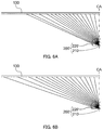
- FIGS. 6A and 6B are schematic views illustrating optical paths in a surface light source device having a light flux controlling member including no gate mark;
- FIG. 7A illustrates, in the surface light source device having the light flux controlling member including no gate mark, illuminance distribution on the inner surface of a diffusion plate when light emitted from one light emitting device illuminates the inner surface of the diffusion plate
- FIG. 7B is a plan view of a light flux controlling member according to an embodiment of the present invention for explaining the position of a gate mark
- FIGS. 8A to 8C show simulation of illuminance distribution in surface light source devices according to Comparative Example 1, Comparative Example 2 and the present embodiment, respectively;
- FIG. 9A is a graph showing illuminance on lines F-F in respective FIGS. 8B and 8C
- FIG. 9B is a graph showing illuminance on lines G-G in respective FIGS. 8B and 8C .
- a surface light source device suitable for a backlight of a liquid crystal display apparatus or the like, in which light emitting devices are disposed in a lattice shape.
- the surface light source device may be used as a display apparatus by combining with a display member (e.g., a liquid crystal panel) to be irradiated with light emitted from the surface light source device.
- a display member e.g., a liquid crystal panel
- FIGS. 2A to 4 illustrate a configuration of surface light source device 100 according to an embodiment of the present invention.
- FIG. 2A is a plan view of surface light source device 100 according to the embodiment of the present invention
- FIG. 2B is a front view of the same.
- FIG. 3A is a cross-sectional view taken along line A-A of FIG. 2B
- FIG. 3B is a cross-sectional view taken along line B-B of FIG. 2A .
- FIG. 4 is a partially enlarged cross-sectional view of surface light source device 100 .
- FIG. 4 illustrates a cross section taken along line C-C of FIG. 3A .
- surface light source device 100 includes casing 110 , a plurality of substrates 120 , a plurality of light emitting devices 200 , and diffusion plate 130 .
- Casing 110 is a cuboidal hollow body which includes bottom plate 112 and top plate 114 facing and parallel to each other.
- the inner surface of bottom plate 112 functions as a diffusion and reflection surface.
- Top plate 114 of casing 110 is provided with an opening.
- Light diffusion member 130 is disposed so as to cover the opening, and functions as a light emitting surface of surface light source device 100 .
- the size of the light emitting surface is, for example, about 400 mm ⁇ 700 mm.
- Substrates 120 are fixed on bottom plate 112 of casing 110 in such a manner that they are parallel to each other at regular intervals.
- Light emitting devices 200 are mounted on one substrate 120 in line at regular intervals. This configuration leads to light emitting devices 200 disposed on bottom plate 112 in a lattice shape.
- four substrates 120 each extending in the X-direction are arranged in the Y-direction, in the drawing.
- eight light emitting devices 200 are arranged in the X-direction.
- This configuration leads to 32 light emitting devices 200 disposed in a substantially square lattice shape.
- One large substrate 120 may be disposed in place of the plurality of substrates 120 . In this case, a plurality of light emitting devices 200 is disposed on one substrate 120 in a lattice shape.
- Light emitting devices 200 each include light emitting element 210 and light flux controlling member 220 .
- Light emitting element 210 is a light source of surface light source device 100 , and is mounted on substrate 120 .
- Light emitting element 210 is a light emitting diode (LED), such as a white light emitting diode.
- LED light emitting diode
- Light flux controlling member 220 is a lens, and fixed on substrate 120 .
- Light flux controlling member 220 controls the distribution of light emitted from light emitting element 210 to expand the traveling direction of the light to the surface directions of diffusion plate 130 .
- Light flux controlling member 220 is disposed above light emitting element 210 so that central axis CA of light flux controlling member 220 coincides with optical axis OA of light emitting element 210 (refer to FIG. 4 ).
- Below-described incidence surface 222 and emission surface 226 of light flux controlling member 220 are rotationally symmetric (incidence surface 222 has circular symmetry, and emission surface 226 has four-fold symmetry), and rotation axes of the surfaces coincide with optical axis OA of light emitting element 210 .
- Optical axis OA of light emitting element 210 is a light beam that is in the center of three-dimensional light flux emitted from light emitting element 210 .
- Light flux controlling member 220 is formed by injection molding. Therefore, gate mark 227 is formed on a part of the outer peripheral portion of light flux controlling member 220 .
- any light-transmissive resin which can be molded by injection molding and which can transmit light having a desired wavelength may be used. Examples of the light-transmissive resins include polymethylmethacrylate (PMMA), polycarbonate (PC) and epoxy resin (EP).
- PMMA polymethylmethacrylate
- PC polycarbonate
- EP epoxy resin
- the main feature of surface light source device 100 according to the present embodiment is in the configuration of light flux controlling member 220 . Therefore, light flux controlling member 220 will be described in detail below.
- light emitting devices 200 are disposed so that respective gate marks 227 therein are directed in the same direction (A-direction in the drawings).
- Diffusion plate 130 is a plate-shaped member having light diffusivity, which transmits light emitted from light emitting device 210 while diffusing the light. Diffusion plate 130 is disposed above light emitting devices 200 , and substantially parallel to substrates 120 . Typically, diffusion plate 130 has a size substantially the same as a member to be irradiated (display member), such as a liquid crystal panel.
- diffusion plate 130 is formed of a light-transmissive resin, such as polymethylmethacrylate (PMMA), polycarbonate (PC), polystyrene (PS) or styrene-methylmethacrylate copolymer resin (MS). To confer light diffusivity, fine irregularities are formed on the surface of diffusion plate 130 , or light diffusion elements, such as beads are dispersed inside diffusion plate 130 .
- PMMA polymethylmethacrylate
- PC polycarbonate
- PS polystyrene
- MS styrene-methylmethacrylate copolymer resin
- light flux controlling member 220 expands light emitted from corresponding light emitting element 210 for illuminating a broad range of diffusion plate 130 .
- light distribution characteristics of light flux controlling member 220 in the directions along an array lattice of light emitting devices 210 are different from that in the diagonal directions of the array lattice (A-direction and B-direction). This enables substantially uniform illumination of the inner surface of diffusion plate 130 .
- the light reaching diffusion plate 130 from each light flux controlling member 220 passes through diffusion plate 130 while being diffused. Consequently, surface light source device 100 according to the present invention can uniformly illuminate a planar member to be irradiated (i.e., display member, such as a liquid crystal panel).
- FIGS. 5A to 5D illustrate a configuration of light flux controlling member 220 .
- FIG. 5A is a plan view
- FIG. 5B is a bottom view
- FIG. 5C is a back view of light flux controlling member 220
- FIG. 5D is a cross-sectional view taken along line D-D of FIG. 5A .
- light flux controlling member 220 includes incidence surface 222 that is an inner surface of recess 221 disposed on the substrate 120 side, rear surface 223 , a plurality of legs 224 , a plurality of ejector pin marks 225 , emission surface 226 disposed on the diffusion plate 130 side, and gate mark 227 located on a part of the outer peripheral portion of light flux controlling member 220 .
- Recess 221 is disposed on the substrate 120 side (rear side) so as to intersect central axis CA (optical axis OA of light emitting element 210 ) in light flux controlling member 220 .
- the inner surface of recess 221 functions as incidence surface 222 . That is, incidence surface 222 is disposed so as to intersect central axis CA (optical axis OA).
- Incidence surface 222 allows most of light emitted from light emitting element 210 to enter light flux controlling member 220 while controlling the traveling direction of the light.
- Incidence surface 222 intersects central axis CA of light flux controlling member 220 , and is rotationally symmetric with central axis CA as the rotation axis. In the present embodiment, incidence surface 222 has circular symmetry.
- Rear surface 223 is a flat surface which is on the substrate 120 side, and extends in the direction(s) orthogonal to central axis CA (i.e., radial directions) from the opening edge of recess 221 .
- Recess 221 is formed in a central portion of rear surface 223 .
- Legs 224 are cylindrical members protruding toward the substrate 120 side from rear surface 223 . Legs 224 allow for positioning of incidence surface 222 and emission surface 226 at appropriate places relative to light emitting element 210 .
- Leg 224 may have any height, and for example, about 1 mm.
- the number of legs 224 may be any number that is two or more.
- the number of legs 224 is preferably three or more.
- light flux controlling member 220 includes three legs 224 .
- legs 224 are preferably disposed symmetrically relative to a virtual plane which passes through central axis CA and gate mark 227 , and is parallel to central axis CA.
- Ejector pin marks 225 are formed on rear surface 223 by pushing with ejector pins during release from a mold after the injection molding.
- the size and number of ejector pin marks 225 are not limited, and appropriately selected in consideration of deformation during the release or the like.
- three ejector pin marks 225 are formed on rear surface 223 .
- the portions to be pushed with ejector pins i.e., the positions of ejector pin marks 225
- Emission surface 226 is disposed on the diffusion plate 130 side (front side) of light flux controlling member 220 so as to intersect central axis CA. Emission surface 226 emits the light entering light flux controlling member 220 toward the outside while controlling the traveling direction of the light.
- Emission surface 226 has n-fold symmetry, whose outer edge has a substantially n-polygonal shape (n is the number of the corners of the n-polygonal shape) (where n is an integral number of three or more).
- emission surface 226 has four-fold symmetry, whose outer edge has a substantially quadrangular shape.
- first cross section is defined as a cross section including central axis CA and the midpoint of a side of the substantially n-polygonal shape (for example, a cross section taken along line D-D in FIG. 5A ), and “second cross section” is defined as a cross section including central axis CA and a corner of the substantially n-polygonal shape (for example, a cross section taken along line E-E in FIG. 5A ).
- Emission surface 226 includes first emission surface 226 a positioned in a predetermined range about central axis CA, and second emission surface 226 b continuously formed from the periphery of first emission surface 226 a.
- First emission surface 226 a is a curved surface recessed relative to diffusion plate 130 .
- first emission surface 226 a has the same curvature in the first cross section and the second cross section.
- Second emission surface 226 b is a smoothly curved surface which protrudes toward diffusion plate 130 , and is positioned at the periphery of first emission surface 226 a .
- second emission surface 226 b has curvature smaller in the second cross section than in the first cross section.
- second emission surface 226 b includes overhanging part 226 c which protrudes to the outside in the direction(s) orthogonal to central axis CA compared to the outer edge of second emission surface 226 b .
- Providing overhanging part 226 c allows for further use of part of light emitted from light emitting element 210 , which has a large angle relative to optical axis OA compared to the other part of the light, as light illuminating diffusion plate 130 .
- FIGS. 6A and 6B are schematic views illustrating optical paths in a surface light source device including light emitting device 200 ′ that has light flux controlling member 220 ′ including no gate mark 227 , in place of light flux controlling member 220 .
- the optical paths in the surface light source device including light emitting device 200 ′ that has light flux controlling member 220 ′ including no gate mark 227 are illustrated in FIGS. 6A and 6B .
- the only difference between light flux controlling members 220 and 220 ′ is whether gate mark 227 is present or not.
- FIGS. 6A and 6B illustrate the optical paths in the first cross section and the second cross section, respectively. In FIGS.
- Light beams indicated by the optical paths in FIGS. 6A and 6B are light beams with light emission angles (vertical angles ⁇ ) from 5° to 80° at every 5°.
- light which is emitted from light emitting element 210 at a relatively small light emission angle is controlled, while being expanded, by light flux controlling member 220 ′ to travel toward a region close to central axis CA on the inner surface of diffusion plate 130 .
- This enables uniform irradiation of a region directly above light emitting device 200 ′ with the light emitted from light emitting element 210 at a relatively small light emission angle without forming an excessively bright part directly above light emitting device 200 ′.
- light which is emitted from light emitting element 210 at a large light emission angle is controlled, while being concentrated, by light flux controlling member 220 ′ to travel toward a region further from central axis CA on the inner surface of diffusion plate 130 . Accordingly, the light emitted from light emitting element 210 at a large light emission angle travels toward the edge of a region to be irradiated with the light emitted from one light emitting device 200 ′.
- the convergence of light emitted from light emitting element 210 at a large light emission angle is adjusted so that the brightness of each region to be irradiated becomes substantially the same at the edge and central portion therein, as two regions to be irradiated with light emitted from respective two adjacent light emitting devices 200 ′ overlap at the edges of the regions.
- FIG. 7A illustrates illuminance distribution on the inner surface of diffusion plate 130 irradiated with light emitted from light source device 200 ′ having light flux controlling member 220 ′.
- illuminance distribution is shown also for light emitting device 200 ′ having light flux controlling member 220 ′ including no gate mark 227 in FIG. 7A .
- FIG. 7A light emitted from light emitting device 200 ′ which has light flux controlling member 220 ′ having incidence surface 222 and emission surface 226 illuminates the inner surface of diffusion plate 130 substantially in a shape of a quadrangle.
- horizontal angle ⁇ in each of light emitting devices 200 and 200 ′ is defined as an angle that becomes larger in a clockwise direction with central axis CA as a reference axis and the Y-axis direction, which is orthogonal to central axis CA, as 0°.
- ⁇ is 0°
- ⁇ is 90°.
- the illuminance distribution on the inner surface of diffusion plate 130 has anisotropy such that the light reach further in the direction of at least one predetermined horizontal angle ⁇ (specifically, in the direction corresponding to each corner of the substantially n-polygonal shape) compared to other directions.
- the illuminance distribution on the inner surface of diffusion plate 130 has anisotropy such that the light reach further in the directions of ⁇ of 45° (B-direction), ⁇ of 135° (A-direction), ⁇ of 225° and ⁇ of 315° compared to other directions.
- incidence surface 222 has circular symmetry
- emission surface 226 has four-fold symmetry, whose outer edge has a substantially quadrangular shape.
- Light emitted from light emitting device 200 having light flux controlling member 220 illuminates the inner surface of diffusion plate 130 substantially in a shape of a quadrangle (when light flux controlling member 220 includes no gate mark 227 ).
- incidence surface 222 and emission surface 226 are formed in such a manner that, on the assumption that light is emitted from light emitting device 200 in a state where light flux controlling member 220 includes no gate mark 227 , illuminance distribution on diffusion plate 130 has anisotropy such that the light reaches further in the direction of at least one predetermined horizontal angle ⁇ compared to other directions.
- Gate mark 227 is a mark formed by resin injection on a part of the outer peripheral portion of light flux controlling member 220 when light flux controlling member 220 according to the present embodiment is formed by injection molding.
- Light flux controlling member 220 according to the present embodiment is formed by the side gate in which a gate part is connected to the side surface of light flux controlling member 220 .
- Gate mark 227 may be a remaining gate protruding from the outer peripheral portion of light flux controlling member 220 , or a gate cut part formed on substantially the same plane as the outer peripheral portion of light flux controlling member 220 by cutting the gate so that the gate does not remain. Gate mark 227 may be positioned on the outer peripheral portion of light flux controlling member 220 . For example, gate mark 227 may be formed on a part of the outer peripheral portion of emission surface 226 . When light flux controlling member 220 further includes a flange 228 protruding from the outer edge of emission surface 226 in the direction(s) orthogonal to central axis CA as illustrated in FIG. 5E , gate mark 227 may be formed on a part of the flange 228 . In the present embodiment, gate mark 227 is a remaining gate protruding from the outer peripheral portion of emission surface 226 .
- incidence surface 222 and emission surface 226 are formed in such a manner that, on the assumption that light is emitted from light emitting device 200 in a state where light flux controlling member 220 includes no gate mark 227 , illuminance distribution on diffusion plate 130 has anisotropy such that the light reaches further in a direction of at least one predetermined horizontal angle ⁇ (as shown in FIG. 7A , angles ⁇ of 45°, 135°, 225° and 315° in the present embodiment) compared to other directions.
- gate mark 227 is located on the outer peripheral portion of light flux controlling member 220 in such a manner that the range of horizontal angles ⁇ (i.e., horizontal-angle- ⁇ range) of gate mark 227 includes one of the at least one predetermined horizontal angle ⁇ (angles ⁇ of 45°, 135°, 225° and 315°). In the present embodiment, gate mark 227 is located so that the range includes ⁇ of 135° as illustrated in FIG. 7B .
- Emission surface 226 has a shape of n-fold symmetry, whose outer edge has a substantially n-polygonal shape (where n is an integral number of three or more), and the range of horizontal angles ⁇ of gate mark 227 includes a horizontal angle ⁇ corresponding to any one of the corners of the substantially n-polygonal shape.
- emission surface 226 having n-fold symmetry with its outer edge having the substantially n-polygonal shape a ridge line connecting central axis CA and each corner of the substantially n-polygonal shape is formed, and light is concentrated to some degree in the direction including the ridge line (at horizontal angle ⁇ ) and thus reaches further.
- emission surface 226 has a shape of four-fold symmetry, whose outer edge has a substantially quadrangular shape, and the range of horizontal angles ⁇ of gate mark 227 includes a horizontal angle ⁇ (135°) corresponding to one of the corners of the substantially quadrangular shape.
- gate mark 227 is located in the direction (of the predetermined horizontal angle ⁇ ) so that emitted light reaches further compared to other directions (of other horizontal angles ⁇ ), in illuminance distribution having anisotropy due to light emitting device 200 ( 200 ′). Since gate mark 227 cannot appropriately control the traveling direction of light, a dark part is more likely to occur in the direction in which gate mark 227 is located. However, the disposition of gate mark 227 in the above manner enables the generation of a dark part due to gate mark 227 to become less prominent.
- horizontal angles ⁇ corresponding to respective corners of the substantially n-polygonal shape can be referred to as horizontal angles ⁇ 1 to ⁇ n.
- the effect of the light emitting devices 200 becomes more remarkable when they are arranged on the bottom surface of surface light source device 100 .
- light emitting devices 200 are disposed in such a manner that a corner, which corresponds to horizontal angle gin and where gate mark 227 is located, at the outer edge of emission surface 226 in light emitting device 200 a faces a corner, which corresponds to one of horizontal angles ⁇ 1 to ⁇ n ⁇ 1 and where gate mark 227 is not located, at the outer edge of emission surface 226 in light emitting device 200 b adjacent to light emitting device 200 a .” That is, between two adjacent light emitting devices 200 , it is preferred to dispose light emitting devices 200 so that angles of the respective outer edges of emission surfaces 226 face each other, but respective gate marks 227 do not face each other.
- the illuminance distribution was simulated for the inner surface of diffusion plate 130 in surface light source device 100 which uses above described light flux controlling member 220 .
- 16 light emitting devices 200 were disposed in a square lattice shape in surface light source device 100 , and all the light emitting devices 200 were lit up.
- FIGS. 8A and 8B show simulation of illuminance distribution in the surface light source devices according to Comparative Example 1 and Comparative Example 2 respectively
- FIG. 8C shows simulation of illuminance distribution in surface light source device 100 according to the present embodiment.
- “+” mark represents the position of a light emitting device.
- FIG. 9A is a graph showing illuminance on lines F-F in respective FIGS. 8B and 8C
- FIG. 9B is a graph showing illuminance on lines G-G in respective FIGS. 8B and 8C .
- the solid line and the broken line show the illuminance in surface light source device 100 according to the present embodiment and the surface light source device according to Comparative Example 2, respectively.
- each light emitting device illuminates the inner surface of diffusion plate 130 substantially in a shape of a quadrangle, and thus regions to be irradiated which are substantially in shapes of quadrangles overlap at the corners of the regions. Further, as shown in FIGS.
- gate mark 227 As gate mark 227 is located at a position corresponding to one of the predetermined horizontal angles ⁇ (angles ⁇ of 45°, 135°, 225° and 315° in the present embodiment), single light emitting device 200 having light flux controlling member 220 according to the present embodiment can suppress luminance unevenness caused by gate mark 227 regardless of the direction of light flux controlling member 220 .
- surface light source device 100 uses light flux controlling member 220 having gate mark 227 formed in a predetermined direction, and therefore can suppress luminance unevenness caused by a gate mark regardless of the direction of light flux controlling member 220 .
- the outer edge of emission surface 226 is formed substantially in a shape of a quadrangle; however, the present invention is not limited to this configuration.
- the outer edge of an emission surface may be in a shape having only one corner (edge) in the direction of one horizontal angle ⁇ , such as a drop shape.
- a gate mark formed at a position corresponding to the corner can compensate for a dark part, using a tendency of a bright part which is more likely to be generated in the direction of the corner.
- the surface light source device, display apparatus, and light flux controlling member according to the present invention may be employed, for example, in a backlight of a liquid crystal display apparatus or a general lighting.
Landscapes
- Physics & Mathematics (AREA)
- Nonlinear Science (AREA)
- Engineering & Computer Science (AREA)
- General Engineering & Computer Science (AREA)
- Mathematical Physics (AREA)
- Chemical & Material Sciences (AREA)
- Crystallography & Structural Chemistry (AREA)
- General Physics & Mathematics (AREA)
- Optics & Photonics (AREA)
- Planar Illumination Modules (AREA)
- Liquid Crystal (AREA)
Applications Claiming Priority (3)
| Application Number | Priority Date | Filing Date | Title |
|---|---|---|---|
| JP2016-068400 | 2016-03-30 | ||
| JP2016068400A JP6762747B2 (ja) | 2016-03-30 | 2016-03-30 | 面光源装置および表示装置 |
| PCT/JP2017/000527 WO2017168930A1 (ja) | 2016-03-30 | 2017-01-11 | 面光源装置、表示装置および光束制御部材 |
Publications (2)
| Publication Number | Publication Date |
|---|---|
| US20190113806A1 US20190113806A1 (en) | 2019-04-18 |
| US10627675B2 true US10627675B2 (en) | 2020-04-21 |
Family
ID=59963977
Family Applications (1)
| Application Number | Title | Priority Date | Filing Date |
|---|---|---|---|
| US16/090,333 Expired - Fee Related US10627675B2 (en) | 2016-03-30 | 2017-01-11 | Planar light source device, display device and light flux control member |
Country Status (4)
| Country | Link |
|---|---|
| US (1) | US10627675B2 (ja) |
| JP (1) | JP6762747B2 (ja) |
| CN (1) | CN108884974B (ja) |
| WO (1) | WO2017168930A1 (ja) |
Families Citing this family (4)
| Publication number | Priority date | Publication date | Assignee | Title |
|---|---|---|---|---|
| JP6974729B2 (ja) * | 2018-03-13 | 2021-12-01 | サミー株式会社 | 遊技機 |
| JP6974728B2 (ja) * | 2018-03-13 | 2021-12-01 | サミー株式会社 | 遊技機 |
| JP7001922B2 (ja) * | 2019-03-19 | 2022-01-20 | サミー株式会社 | 遊技機 |
| WO2021054377A1 (ja) * | 2019-09-20 | 2021-03-25 | 株式会社エンプラス | 光束制御部材、発光装置、面光源装置および表示装置 |
Citations (14)
| Publication number | Priority date | Publication date | Assignee | Title |
|---|---|---|---|---|
| JP2011003549A (ja) | 2009-05-20 | 2011-01-06 | Sharp Corp | 光源装置及びこれを備える表示装置、テレビ受像装置 |
| US20110128745A1 (en) * | 2009-11-30 | 2011-06-02 | Fu Zhun Precision Industry (Shen Zhen) Co., Ltd. | Lens and led module using the same |
| US20110194279A1 (en) * | 2010-02-06 | 2011-08-11 | Hung-Pin Kuo | Led lighting device with led lamps protected from falling off |
| US8083380B2 (en) * | 2009-04-17 | 2011-12-27 | Mig Technology Inc. | Integrated structure for optical refractor |
| US20130044496A1 (en) * | 2010-03-26 | 2013-02-21 | Akinobu Seki | Luminous-flux control member and illumination apparatus using the same |
| US20130107542A1 (en) * | 2011-10-31 | 2013-05-02 | Enplas Corporation | Light flux controlling member, light emitting apparatus, surface light source apparatus and display apparatus |
| US20140009944A1 (en) * | 2012-07-04 | 2014-01-09 | Enplas Corporation | Light flux controlling member, light emitting apparatus, surface light source apparatus, and display apparatus |
| US20140301085A1 (en) * | 2013-04-04 | 2014-10-09 | Seoul Semiconductor Co., Ltd. | Lens and light emitting module for surface illumination |
| US8876350B2 (en) * | 2009-05-20 | 2014-11-04 | Sharp Kabushiki Kaisha | Light source device and display device provided with same |
| US20150029727A1 (en) * | 2012-05-03 | 2015-01-29 | Nalux Co., Ltd. | Optical element |
| US20150211713A1 (en) * | 2014-01-28 | 2015-07-30 | Enplas Corporation | Surface light source device and display apparatus |
| US20150219286A1 (en) * | 2014-02-06 | 2015-08-06 | Samsung Display Co., Ltd. | Led light source package |
| US20150262518A1 (en) * | 2013-03-15 | 2015-09-17 | General Led, Inc. | LED Light Engine for Signage |
| US20150323729A1 (en) * | 2014-05-08 | 2015-11-12 | Enplas Corporation | Light emitting device, surface light source device and display apparatus |
Family Cites Families (5)
| Publication number | Priority date | Publication date | Assignee | Title |
|---|---|---|---|---|
| JP4863357B2 (ja) * | 2006-01-24 | 2012-01-25 | 株式会社エンプラス | 発光装置、面光源装置、表示装置及び光束制御部材 |
| JP2011018863A (ja) * | 2009-07-10 | 2011-01-27 | Sharp Corp | 発光素子モジュール及びその製造方法、並びに、バックライト装置 |
| JP5396606B2 (ja) * | 2009-09-17 | 2014-01-22 | 株式会社エンプラス | 面光源装置及び表示装置 |
| JP5500609B2 (ja) * | 2012-09-12 | 2014-05-21 | 雷笛克光學股▲ふん▼有限公司 | 正方形の光形を形成する光学レンズ |
| CN104296072A (zh) * | 2014-10-09 | 2015-01-21 | 青岛海信电器股份有限公司 | 一种发光器件及背光源 |
-
2016
- 2016-03-30 JP JP2016068400A patent/JP6762747B2/ja active Active
-
2017
- 2017-01-11 CN CN201780020031.5A patent/CN108884974B/zh not_active Expired - Fee Related
- 2017-01-11 WO PCT/JP2017/000527 patent/WO2017168930A1/ja active Application Filing
- 2017-01-11 US US16/090,333 patent/US10627675B2/en not_active Expired - Fee Related
Patent Citations (14)
| Publication number | Priority date | Publication date | Assignee | Title |
|---|---|---|---|---|
| US8083380B2 (en) * | 2009-04-17 | 2011-12-27 | Mig Technology Inc. | Integrated structure for optical refractor |
| US8876350B2 (en) * | 2009-05-20 | 2014-11-04 | Sharp Kabushiki Kaisha | Light source device and display device provided with same |
| JP2011003549A (ja) | 2009-05-20 | 2011-01-06 | Sharp Corp | 光源装置及びこれを備える表示装置、テレビ受像装置 |
| US20110128745A1 (en) * | 2009-11-30 | 2011-06-02 | Fu Zhun Precision Industry (Shen Zhen) Co., Ltd. | Lens and led module using the same |
| US20110194279A1 (en) * | 2010-02-06 | 2011-08-11 | Hung-Pin Kuo | Led lighting device with led lamps protected from falling off |
| US20130044496A1 (en) * | 2010-03-26 | 2013-02-21 | Akinobu Seki | Luminous-flux control member and illumination apparatus using the same |
| US20130107542A1 (en) * | 2011-10-31 | 2013-05-02 | Enplas Corporation | Light flux controlling member, light emitting apparatus, surface light source apparatus and display apparatus |
| US20150029727A1 (en) * | 2012-05-03 | 2015-01-29 | Nalux Co., Ltd. | Optical element |
| US20140009944A1 (en) * | 2012-07-04 | 2014-01-09 | Enplas Corporation | Light flux controlling member, light emitting apparatus, surface light source apparatus, and display apparatus |
| US20150262518A1 (en) * | 2013-03-15 | 2015-09-17 | General Led, Inc. | LED Light Engine for Signage |
| US20140301085A1 (en) * | 2013-04-04 | 2014-10-09 | Seoul Semiconductor Co., Ltd. | Lens and light emitting module for surface illumination |
| US20150211713A1 (en) * | 2014-01-28 | 2015-07-30 | Enplas Corporation | Surface light source device and display apparatus |
| US20150219286A1 (en) * | 2014-02-06 | 2015-08-06 | Samsung Display Co., Ltd. | Led light source package |
| US20150323729A1 (en) * | 2014-05-08 | 2015-11-12 | Enplas Corporation | Light emitting device, surface light source device and display apparatus |
Non-Patent Citations (1)
| Title |
|---|
| International Search Report from International Application No. PCT/JP2017/000527 dated Mar. 21, 2017. |
Also Published As
| Publication number | Publication date |
|---|---|
| JP2017183077A (ja) | 2017-10-05 |
| US20190113806A1 (en) | 2019-04-18 |
| CN108884974B (zh) | 2021-01-26 |
| CN108884974A (zh) | 2018-11-23 |
| WO2017168930A1 (ja) | 2017-10-05 |
| JP6762747B2 (ja) | 2020-09-30 |
Similar Documents
| Publication | Publication Date | Title |
|---|---|---|
| JP6046398B2 (ja) | 面光源装置および表示装置 | |
| JP5957364B2 (ja) | 光束制御部材、発光装置、面光源装置および表示装置 | |
| JP5889101B2 (ja) | 光束制御部材、発光装置および照明装置 | |
| JP6356997B2 (ja) | 光束制御部材、発光装置、面光源装置および表示装置 | |
| US10627675B2 (en) | Planar light source device, display device and light flux control member | |
| US10393343B2 (en) | Light flux control member, light-emitting device, and area light source device | |
| JP6629601B2 (ja) | 光束制御部材、発光装置、面光源装置および表示装置 | |
| US10634296B2 (en) | Luminous flux control member, light-emitting device, planar light source device, and display device | |
| WO2018155676A1 (ja) | 発光装置、面光源装置および表示装置 | |
| WO2019044968A1 (ja) | 発光装置、面光源装置および表示装置 | |
| US10718974B2 (en) | Planar light source device and display device | |
| JP6983116B2 (ja) | 面光源装置および表示装置 | |
| US11079628B2 (en) | Light emitting device having luminous flux control member with recess radially distant from a light incident surface | |
| JP2017072719A (ja) | 光束制御部材、発光装置、面光源装置および表示装置 | |
| WO2018135407A1 (ja) | 光束制御部材、発光装置、面光源装置および表示装置 | |
| US10466533B2 (en) | Light flux control member, light-emitting device, surface light source device and display device | |
| JP2018036407A (ja) | 光束制御部材、発光装置、面光源装置および表示装置 | |
| WO2021070343A1 (ja) | 面光源装置および表示装置 | |
| JP6619669B2 (ja) | 光束制御部材、発光装置、光源装置及び表示装置 | |
| JP2023023939A (ja) | 面光源装置および表示装置 | |
| JP2022156518A (ja) | 光束制御部材、発光装置、面光源装置および表示装置 | |
| JP2021108248A (ja) | 面光源装置および表示装置 | |
| JP2022111712A (ja) | 光束制御部材、発光装置、面光源装置および表示装置 | |
| JP2022111718A (ja) | 光束制御部材、発光装置、面光源装置および表示装置 |
Legal Events
| Date | Code | Title | Description |
|---|---|---|---|
| FEPP | Fee payment procedure |
Free format text: ENTITY STATUS SET TO UNDISCOUNTED (ORIGINAL EVENT CODE: BIG.); ENTITY STATUS OF PATENT OWNER: LARGE ENTITY |
|
| AS | Assignment |
Owner name: ENPLAS CORPORATION, JAPAN Free format text: ASSIGNMENT OF ASSIGNORS INTEREST;ASSIGNOR:HIRAKA, KENSUKE;REEL/FRAME:047030/0783 Effective date: 20180704 |
|
| STPP | Information on status: patent application and granting procedure in general |
Free format text: DOCKETED NEW CASE - READY FOR EXAMINATION |
|
| STPP | Information on status: patent application and granting procedure in general |
Free format text: NON FINAL ACTION MAILED |
|
| STPP | Information on status: patent application and granting procedure in general |
Free format text: NOTICE OF ALLOWANCE MAILED -- APPLICATION RECEIVED IN OFFICE OF PUBLICATIONS |
|
| STCF | Information on status: patent grant |
Free format text: PATENTED CASE |
|
| CC | Certificate of correction | ||
| FEPP | Fee payment procedure |
Free format text: MAINTENANCE FEE REMINDER MAILED (ORIGINAL EVENT CODE: REM.); ENTITY STATUS OF PATENT OWNER: LARGE ENTITY |