US10586489B2 - Display device, display device driving method, display element, and electronic apparatus - Google Patents
Display device, display device driving method, display element, and electronic apparatus Download PDFInfo
- Publication number
- US10586489B2 US10586489B2 US15/768,134 US201615768134A US10586489B2 US 10586489 B2 US10586489 B2 US 10586489B2 US 201615768134 A US201615768134 A US 201615768134A US 10586489 B2 US10586489 B2 US 10586489B2
- Authority
- US
- United States
- Prior art keywords
- node
- switching transistor
- voltage
- capacitor
- transistor
- Prior art date
- Legal status (The legal status is an assumption and is not a legal conclusion. Google has not performed a legal analysis and makes no representation as to the accuracy of the status listed.)
- Expired - Fee Related
Links
- 238000000034 method Methods 0.000 title claims description 29
- 239000003990 capacitor Substances 0.000 claims abstract description 383
- 239000013256 coordination polymer Substances 0.000 description 60
- 239000008186 active pharmaceutical agent Substances 0.000 description 58
- 239000010410 layer Substances 0.000 description 42
- 238000012545 processing Methods 0.000 description 36
- 230000007423 decrease Effects 0.000 description 23
- 230000008859 change Effects 0.000 description 16
- 238000010586 diagram Methods 0.000 description 16
- 239000006185 dispersion Substances 0.000 description 15
- 239000011229 interlayer Substances 0.000 description 12
- 239000000463 material Substances 0.000 description 12
- 239000000758 substrate Substances 0.000 description 10
- VYPSYNLAJGMNEJ-UHFFFAOYSA-N Silicium dioxide Chemical compound O=[Si]=O VYPSYNLAJGMNEJ-UHFFFAOYSA-N 0.000 description 8
- 239000011521 glass Substances 0.000 description 8
- 239000011159 matrix material Substances 0.000 description 7
- 230000008901 benefit Effects 0.000 description 6
- 230000011514 reflex Effects 0.000 description 5
- 239000004065 semiconductor Substances 0.000 description 5
- 229910052681 coesite Inorganic materials 0.000 description 4
- 239000000470 constituent Substances 0.000 description 4
- 229910052906 cristobalite Inorganic materials 0.000 description 4
- 230000005525 hole transport Effects 0.000 description 4
- 239000000377 silicon dioxide Substances 0.000 description 4
- 229910052682 stishovite Inorganic materials 0.000 description 4
- 229910052905 tridymite Inorganic materials 0.000 description 4
- KKCBUQHMOMHUOY-UHFFFAOYSA-N Na2O Inorganic materials [O-2].[Na+].[Na+] KKCBUQHMOMHUOY-UHFFFAOYSA-N 0.000 description 3
- 230000000694 effects Effects 0.000 description 3
- 230000003071 parasitic effect Effects 0.000 description 3
- 230000003287 optical effect Effects 0.000 description 2
- 239000011368 organic material Substances 0.000 description 2
- 239000005020 polyethylene terephthalate Substances 0.000 description 2
- 229920000139 polyethylene terephthalate Polymers 0.000 description 2
- 230000008569 process Effects 0.000 description 2
- 230000009467 reduction Effects 0.000 description 2
- 229920012266 Poly(ether sulfone) PES Polymers 0.000 description 1
- 239000004642 Polyimide Substances 0.000 description 1
- CDBYLPFSWZWCQE-UHFFFAOYSA-L Sodium Carbonate Chemical compound [Na+].[Na+].[O-]C([O-])=O CDBYLPFSWZWCQE-UHFFFAOYSA-L 0.000 description 1
- 229910045601 alloy Inorganic materials 0.000 description 1
- 239000000956 alloy Substances 0.000 description 1
- 229910021417 amorphous silicon Inorganic materials 0.000 description 1
- 239000005388 borosilicate glass Substances 0.000 description 1
- 238000000576 coating method Methods 0.000 description 1
- 230000000295 complement effect Effects 0.000 description 1
- 229920001940 conductive polymer Polymers 0.000 description 1
- 239000004020 conductor Substances 0.000 description 1
- 238000005401 electroluminescence Methods 0.000 description 1
- 229910052839 forsterite Inorganic materials 0.000 description 1
- 239000012535 impurity Substances 0.000 description 1
- 239000005355 lead glass Substances 0.000 description 1
- 239000004973 liquid crystal related substance Substances 0.000 description 1
- HCWCAKKEBCNQJP-UHFFFAOYSA-N magnesium orthosilicate Chemical compound [Mg+2].[Mg+2].[O-][Si]([O-])([O-])[O-] HCWCAKKEBCNQJP-UHFFFAOYSA-N 0.000 description 1
- 239000002184 metal Substances 0.000 description 1
- 239000000203 mixture Substances 0.000 description 1
- 238000012986 modification Methods 0.000 description 1
- 230000004048 modification Effects 0.000 description 1
- 239000012044 organic layer Substances 0.000 description 1
- 239000002245 particle Substances 0.000 description 1
- 239000004417 polycarbonate Substances 0.000 description 1
- 229920000515 polycarbonate Polymers 0.000 description 1
- 229910021420 polycrystalline silicon Inorganic materials 0.000 description 1
- -1 polyethylene terephthalate Polymers 0.000 description 1
- 229920001721 polyimide Polymers 0.000 description 1
- 229920005591 polysilicon Polymers 0.000 description 1
- 239000010409 thin film Substances 0.000 description 1
Images


Classifications
-
- G—PHYSICS
- G09—EDUCATION; CRYPTOGRAPHY; DISPLAY; ADVERTISING; SEALS
- G09G—ARRANGEMENTS OR CIRCUITS FOR CONTROL OF INDICATING DEVICES USING STATIC MEANS TO PRESENT VARIABLE INFORMATION
- G09G3/00—Control arrangements or circuits, of interest only in connection with visual indicators other than cathode-ray tubes
- G09G3/20—Control arrangements or circuits, of interest only in connection with visual indicators other than cathode-ray tubes for presentation of an assembly of a number of characters, e.g. a page, by composing the assembly by combination of individual elements arranged in a matrix no fixed position being assigned to or needed to be assigned to the individual characters or partial characters
- G09G3/22—Control arrangements or circuits, of interest only in connection with visual indicators other than cathode-ray tubes for presentation of an assembly of a number of characters, e.g. a page, by composing the assembly by combination of individual elements arranged in a matrix no fixed position being assigned to or needed to be assigned to the individual characters or partial characters using controlled light sources
- G09G3/30—Control arrangements or circuits, of interest only in connection with visual indicators other than cathode-ray tubes for presentation of an assembly of a number of characters, e.g. a page, by composing the assembly by combination of individual elements arranged in a matrix no fixed position being assigned to or needed to be assigned to the individual characters or partial characters using controlled light sources using electroluminescent panels
- G09G3/32—Control arrangements or circuits, of interest only in connection with visual indicators other than cathode-ray tubes for presentation of an assembly of a number of characters, e.g. a page, by composing the assembly by combination of individual elements arranged in a matrix no fixed position being assigned to or needed to be assigned to the individual characters or partial characters using controlled light sources using electroluminescent panels semiconductive, e.g. using light-emitting diodes [LED]
- G09G3/3208—Control arrangements or circuits, of interest only in connection with visual indicators other than cathode-ray tubes for presentation of an assembly of a number of characters, e.g. a page, by composing the assembly by combination of individual elements arranged in a matrix no fixed position being assigned to or needed to be assigned to the individual characters or partial characters using controlled light sources using electroluminescent panels semiconductive, e.g. using light-emitting diodes [LED] organic, e.g. using organic light-emitting diodes [OLED]
- G09G3/3225—Control arrangements or circuits, of interest only in connection with visual indicators other than cathode-ray tubes for presentation of an assembly of a number of characters, e.g. a page, by composing the assembly by combination of individual elements arranged in a matrix no fixed position being assigned to or needed to be assigned to the individual characters or partial characters using controlled light sources using electroluminescent panels semiconductive, e.g. using light-emitting diodes [LED] organic, e.g. using organic light-emitting diodes [OLED] using an active matrix
- G09G3/3233—Control arrangements or circuits, of interest only in connection with visual indicators other than cathode-ray tubes for presentation of an assembly of a number of characters, e.g. a page, by composing the assembly by combination of individual elements arranged in a matrix no fixed position being assigned to or needed to be assigned to the individual characters or partial characters using controlled light sources using electroluminescent panels semiconductive, e.g. using light-emitting diodes [LED] organic, e.g. using organic light-emitting diodes [OLED] using an active matrix with pixel circuitry controlling the current through the light-emitting element
-
- H—ELECTRICITY
- H10—SEMICONDUCTOR DEVICES; ELECTRIC SOLID-STATE DEVICES NOT OTHERWISE PROVIDED FOR
- H10K—ORGANIC ELECTRIC SOLID-STATE DEVICES
- H10K50/00—Organic light-emitting devices
-
- G—PHYSICS
- G09—EDUCATION; CRYPTOGRAPHY; DISPLAY; ADVERTISING; SEALS
- G09G—ARRANGEMENTS OR CIRCUITS FOR CONTROL OF INDICATING DEVICES USING STATIC MEANS TO PRESENT VARIABLE INFORMATION
- G09G2300/00—Aspects of the constitution of display devices
- G09G2300/08—Active matrix structure, i.e. with use of active elements, inclusive of non-linear two terminal elements, in the pixels together with light emitting or modulating elements
- G09G2300/0809—Several active elements per pixel in active matrix panels
- G09G2300/0819—Several active elements per pixel in active matrix panels used for counteracting undesired variations, e.g. feedback or autozeroing
-
- G—PHYSICS
- G09—EDUCATION; CRYPTOGRAPHY; DISPLAY; ADVERTISING; SEALS
- G09G—ARRANGEMENTS OR CIRCUITS FOR CONTROL OF INDICATING DEVICES USING STATIC MEANS TO PRESENT VARIABLE INFORMATION
- G09G2300/00—Aspects of the constitution of display devices
- G09G2300/08—Active matrix structure, i.e. with use of active elements, inclusive of non-linear two terminal elements, in the pixels together with light emitting or modulating elements
- G09G2300/0876—Supplementary capacities in pixels having special driving circuits and electrodes instead of being connected to common electrode or ground; Use of additional capacitively coupled compensation electrodes
-
- G—PHYSICS
- G09—EDUCATION; CRYPTOGRAPHY; DISPLAY; ADVERTISING; SEALS
- G09G—ARRANGEMENTS OR CIRCUITS FOR CONTROL OF INDICATING DEVICES USING STATIC MEANS TO PRESENT VARIABLE INFORMATION
- G09G2310/00—Command of the display device
- G09G2310/02—Addressing, scanning or driving the display screen or processing steps related thereto
- G09G2310/0243—Details of the generation of driving signals
- G09G2310/0251—Precharge or discharge of pixel before applying new pixel voltage
-
- G—PHYSICS
- G09—EDUCATION; CRYPTOGRAPHY; DISPLAY; ADVERTISING; SEALS
- G09G—ARRANGEMENTS OR CIRCUITS FOR CONTROL OF INDICATING DEVICES USING STATIC MEANS TO PRESENT VARIABLE INFORMATION
- G09G2310/00—Command of the display device
- G09G2310/06—Details of flat display driving waveforms
-
- G—PHYSICS
- G09—EDUCATION; CRYPTOGRAPHY; DISPLAY; ADVERTISING; SEALS
- G09G—ARRANGEMENTS OR CIRCUITS FOR CONTROL OF INDICATING DEVICES USING STATIC MEANS TO PRESENT VARIABLE INFORMATION
- G09G2320/00—Control of display operating conditions
- G09G2320/02—Improving the quality of display appearance
- G09G2320/0233—Improving the luminance or brightness uniformity across the screen
-
- G—PHYSICS
- G09—EDUCATION; CRYPTOGRAPHY; DISPLAY; ADVERTISING; SEALS
- G09G—ARRANGEMENTS OR CIRCUITS FOR CONTROL OF INDICATING DEVICES USING STATIC MEANS TO PRESENT VARIABLE INFORMATION
- G09G2330/00—Aspects of power supply; Aspects of display protection and defect management
- G09G2330/02—Details of power systems and of start or stop of display operation
- G09G2330/021—Power management, e.g. power saving
-
- G—PHYSICS
- G09—EDUCATION; CRYPTOGRAPHY; DISPLAY; ADVERTISING; SEALS
- G09G—ARRANGEMENTS OR CIRCUITS FOR CONTROL OF INDICATING DEVICES USING STATIC MEANS TO PRESENT VARIABLE INFORMATION
- G09G3/00—Control arrangements or circuits, of interest only in connection with visual indicators other than cathode-ray tubes
- G09G3/20—Control arrangements or circuits, of interest only in connection with visual indicators other than cathode-ray tubes for presentation of an assembly of a number of characters, e.g. a page, by composing the assembly by combination of individual elements arranged in a matrix no fixed position being assigned to or needed to be assigned to the individual characters or partial characters
- G09G3/22—Control arrangements or circuits, of interest only in connection with visual indicators other than cathode-ray tubes for presentation of an assembly of a number of characters, e.g. a page, by composing the assembly by combination of individual elements arranged in a matrix no fixed position being assigned to or needed to be assigned to the individual characters or partial characters using controlled light sources
- G09G3/30—Control arrangements or circuits, of interest only in connection with visual indicators other than cathode-ray tubes for presentation of an assembly of a number of characters, e.g. a page, by composing the assembly by combination of individual elements arranged in a matrix no fixed position being assigned to or needed to be assigned to the individual characters or partial characters using controlled light sources using electroluminescent panels
- G09G3/32—Control arrangements or circuits, of interest only in connection with visual indicators other than cathode-ray tubes for presentation of an assembly of a number of characters, e.g. a page, by composing the assembly by combination of individual elements arranged in a matrix no fixed position being assigned to or needed to be assigned to the individual characters or partial characters using controlled light sources using electroluminescent panels semiconductive, e.g. using light-emitting diodes [LED]
- G09G3/3208—Control arrangements or circuits, of interest only in connection with visual indicators other than cathode-ray tubes for presentation of an assembly of a number of characters, e.g. a page, by composing the assembly by combination of individual elements arranged in a matrix no fixed position being assigned to or needed to be assigned to the individual characters or partial characters using controlled light sources using electroluminescent panels semiconductive, e.g. using light-emitting diodes [LED] organic, e.g. using organic light-emitting diodes [OLED]
- G09G3/3275—Details of drivers for data electrodes
- G09G3/3291—Details of drivers for data electrodes in which the data driver supplies a variable data voltage for setting the current through, or the voltage across, the light-emitting elements
Definitions
- the present disclosure relates to a display device, a display device driving method, a display element, and an electronic apparatus.
- a display element provided with a current-driven light-emitting unit, and a display device provided with the display element, are well known.
- a display element provided with a light-emitting unit that uses electroluminescence of an organic material (hereinafter, may be merely referred to as “organic EL display element”) attracts attention as a display element that is capable of high-luminance light emission by low-voltage DC driving.
- an organic EL display element driven by the active matrix method is provided with not only a light-emitting unit that includes an organic layer including a light-emitting layer and the like, but also a driving circuit having a driving transistor for driving the light-emitting unit.
- a value of a current flowing through the driving transistor is influenced not only by a voltage of a gate electrode with respect to a source region of the driving transistor (so-called a voltage between the gate and the source) but also by a threshold voltage of the driving transistor.
- the threshold voltage of the driving transistor disperses on a display element basis, and therefore causes uneven brightness.
- Patent Document 1 discloses the feature of performing the operation of canceling an influence, which is exerted by the dispersion in threshold voltage of a driving transistor, every time a video signal is written to a display element.
- the operation of canceling the influence, which is exerted by the dispersion in threshold voltage of a driving transistor, every time a video signal is written becomes a factor for increasing the power consumption of a display device.
- the power consumption of an electronic apparatus is desired to be low. Accordingly, a reduction in power consumption of a display device is also expected.
- an object of the present invention is to provide: a display device that is capable of further reducing the power consumption while canceling an influence exerted by the dispersion in threshold voltage of a driving transistor; a method for driving the display device; a display element; and an electronic apparatus.
- a display device includes: a display unit in which display elements are arranged; and a drive unit for driving the display unit, in which:
- the display elements each include: a current-driven light-emitting unit; a capacitor unit including a first capacitor and a second capacitor; an n-channel driving transistor that causes a current corresponding to a voltage held by the capacitor unit to flow through the light-emitting unit; and a first switching transistor that writes a video signal voltage to the capacitor unit;
- one end of the first capacitor is connected to a gate electrode of the driving transistor to form a first node
- the other end of the first capacitor is connected to one end of the second capacitor to form a second node
- the other end of the second capacitor is connected to one end of the light-emitting unit, and to the other source/drain region of the driving transistor to form a third node;
- one source/drain region is connected to an electric supply line, and the other source/drain region is connected to the light-emitting unit;
- one source/drain region is connected to a data line, and the other source/drain region is connected to the third node;
- the drive unit writes a video signal voltage to the second capacitor through the first switching transistor in a conducting state.
- the display device including: a display unit in which display elements are arranged; and a drive unit for driving the display unit, in which:
- the display elements each include: a current-driven light-emitting unit; a capacitor unit including a first capacitor and a second capacitor; an n-channel driving transistor that causes a current corresponding to a voltage held by the capacitor unit to flow through the light-emitting unit; and a first switching transistor that writes a video signal voltage to the capacitor unit;
- one end of the first capacitor is connected to a gate electrode of the driving transistor to form a first node
- the other end of the first capacitor is connected to one end of the second capacitor to form a second node
- the other end of the second capacitor is connected to one end of the light-emitting unit, and to the other source/drain region of the driving transistor to form a third node;
- one source/drain region is connected to an electric supply line, and the other source/drain region is connected to the light-emitting unit;
- one source/drain region is connected to a data line, and the other source/drain region is connected to the third node;
- the drive unit writes a video signal voltage to the second capacitor through the first switching transistor in a conducting state.
- a display element according to the present disclosure includes:
- a current-driven light-emitting unit a capacitor unit including a first capacitor and a second capacitor; an n-channel driving transistor that causes a current corresponding to a voltage held by the capacitor unit to flow through the light-emitting unit; and a first switching transistor that writes a video signal voltage to the capacitor unit;
- one end of the first capacitor is connected to a gate electrode of the driving transistor to form a first node
- the other end of the first capacitor is connected to one end of the second capacitor to form a second node
- the other end of the second capacitor is connected to one end of the light-emitting unit, and to the other source/drain region of the driving transistor to form a third node;
- one source/drain region is connected to an electric supply line, and the other source/drain region is connected to the light-emitting unit;
- one source/drain region is connected to a data line, and the other source/drain region is connected to the third node;
- a video signal voltage is written to the second capacitor through the first switching transistor in a conducting state.
- an electronic apparatus includes a display device, in which:
- the display device includes: a display unit in which display elements are arranged; and a drive unit for driving the display unit;
- the display elements each include: a current-driven light-emitting unit; a capacitor unit including a first capacitor and a second capacitor; an n-channel driving transistor that causes a current corresponding to a voltage held by the capacitor unit to flow through the light-emitting unit; and a first switching transistor that writes a video signal voltage to the capacitor unit;
- one end of the first capacitor is connected to a gate electrode of the driving transistor to form a first node
- the other end of the first capacitor is connected to one end of the second capacitor to form a second node
- the other end of the second capacitor is connected to one end of the light-emitting unit, and to the other source/drain region of the driving transistor to form a third node;
- one source/drain region is connected to an electric supply line, and the other source/drain region is connected to the light-emitting unit;
- one source/drain region is connected to a data line, and the other source/drain region is connected to the third node;
- the drive unit writes a video signal voltage to the second capacitor through the first switching transistor in a conducting state.
- the display device in a state in which the first capacitor holds a voltage corresponding to a threshold voltage of the driving transistor, a video signal voltage is written to the second capacitor through the first switching transistor in a conducting state.
- This enables a frequency of operations of holding, in the first capacitor, a voltage corresponding to a threshold voltage of the driving transistor to be reduced. Therefore, the power consumption can be further reduced while canceling an influence exerted by the dispersion in threshold voltage of the driving transistor.
- the effects described herein are not necessarily limited, and may be any one of the effects described in the present disclosure.
- FIG. 1 is a conceptual diagram illustrating a display device according to a first embodiment.
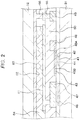
- FIG. 2 is a schematic partial cross-sectional view illustrating a part including a display element in the display unit.
- FIG. 3 is a schematic timing chart illustrating the operation of the display device according to the first embodiment, more specifically, the operation of the (n, m)th display element of the display device.
- FIG. 4A and FIG. 4B are drawings each schematically illustrating conducting state/non-conducting state and the like of each transistor that is included in a driving circuit of the display element of the display device according to the first embodiment.
- FIG. 5A and FIG. 5B are drawings each schematically illustrating conducting state/non-conducting state and the like of each transistor that is included in the driving circuit of the display element of the display device according to the first embodiment.
- FIG. 6A and FIG. 6B are drawings each schematically illustrating conducting state/non-conducting state and the like of each transistor that is included in the driving circuit of the display element of the display device according to the first embodiment.
- FIG. 7A and FIG. 7B are drawings each schematically illustrating conducting state/non-conducting state and the like of each transistor that is included in the driving circuit of the display element of the display device according to the first embodiment.
- FIG. 8A and FIG. 8B are drawings each schematically illustrating conducting state/non-conducting state and the like of each transistor that is included in the driving circuit of the display element of the display device according to the first embodiment.
- FIG. 9 is a schematic timing chart illustrating the operation of a display device according to a second embodiment, more specifically, the operation of the (n, m)th display element of the display device.
- FIG. 10A and FIG. 10B are drawings each schematically illustrating conducting state/non-conducting state and the like of each transistor that is included in a driving circuit of the display element of the display device according to the second embodiment.
- FIG. 11 is a conceptual diagram illustrating a display device according to a third embodiment.
- FIG. 12 is a schematic timing chart illustrating the operation of the display device according to the third embodiment, more specifically, the operation of the (n, m)th display element of the display device.
- FIG. 13A and FIG. 13B are drawings each schematically illustrating conducting state/non-conducting state and the like of each transistor that is included in a driving circuit of the display element of the display device according to the third embodiment.
- FIG. 14A and FIG. 14B are drawings each schematically illustrating conducting state/non-conducting state and the like of each transistor that is included in the driving circuit of the display element of the display device according to the third embodiment.
- FIG. 15A and FIG. 15B are drawings each schematically illustrating conducting state/non-conducting state and the like of each transistor that is included in the driving circuit of the display element of the display device according to the third embodiment.
- FIG. 16A and FIG. 16B are drawings each schematically illustrating conducting state/non-conducting state and the like of each transistor that is included in the driving circuit of the display element of the display device according to the third embodiment.
- FIG. 17A and FIG. 17B are drawings each schematically illustrating conducting state/non-conducting state and the like of each transistor that is included in the driving circuit of the display element of the display device according to the third embodiment.
- FIG. 18 is a conceptual diagram illustrating a display device according to a fourth embodiment.
- FIG. 19 is a schematic timing chart illustrating the operation of the display device according to the fourth embodiment, more specifically, the operation of the (n, m)th display element of the display device.
- FIG. 20A and FIG. 20B are drawings each schematically illustrating conducting state/non-conducting state and the like of each transistor that is included in a driving circuit of the display element of the display device according to the fourth embodiment.
- FIG. 21A and FIG. 21B are drawings each schematically illustrating conducting state/non-conducting state and the like of each transistor that is included in the driving circuit of the display element of the display device according to the fourth embodiment.
- FIG. 22A and FIG. 22B are drawings each schematically illustrating conducting state/non-conducting state and the like of each transistor that is included in the driving circuit of the display element of the display device according to the fourth embodiment.
- FIG. 23A and FIG. 23B are drawings each schematically illustrating conducting state/non-conducting state and the like of each transistor that is included in the driving circuit of the display element of the display device according to the fourth embodiment.
- FIG. 24A and FIG. 24B are drawings each schematically illustrating conducting state/non-conducting state and the like of each transistor that is included in the driving circuit of the display element of the display device according to the fourth embodiment.
- FIG. 25 is a conceptual diagram illustrating a display device according to a fifth embodiment.
- FIG. 26 is a schematic timing chart illustrating the operation of the display device according to the fifth embodiment, more specifically, the operation of the (n, m)th display element of the display device.
- FIG. 27A and FIG. 27B are drawings each schematically illustrating conducting state/non-conducting state and the like of each transistor that is included in a driving circuit of the display element of the display device according to the fifth embodiment.
- FIG. 28A and FIG. 28B are drawings each schematically illustrating conducting state/non-conducting state and the like of each transistor that is included in the driving circuit of the display element of the display device according to the fifth embodiment.
- FIG. 29A and FIG. 29B are drawings each schematically illustrating conducting state/non-conducting state and the like of each transistor that is included in the driving circuit of the display element of the display device according to the fifth embodiment.
- FIG. 30A and FIG. 30B are drawings each schematically illustrating conducting state/non-conducting state and the like of each transistor that is included in the driving circuit of the display element of the display device according to the fifth embodiment.
- FIG. 31A and FIG. 31B are drawings each schematically illustrating conducting state/non-conducting state and the like of each transistor that is included in the driving circuit of the display element of the display device according to the fifth embodiment.
- FIG. 32 is a schematic timing chart illustrating the operation of a display device according to a sixth embodiment, more specifically, the operation of the (n, m)th display element of the display device.
- FIG. 33A and FIG. 33B are drawings each schematically illustrating conducting state/non-conducting state and the like of each transistor that is included in a driving circuit of the display element of the display device according to the sixth embodiment.
- FIG. 34 is a conceptual diagram illustrating a display device according to a seventh embodiment.
- FIG. 35 is a schematic timing chart illustrating the operation of the display device according to the seventh embodiment, more specifically, the operation of the (n, m)th display element of the display device.
- FIG. 36A and FIG. 36B are drawings each schematically illustrating conducting state/non-conducting state and the like of each transistor that is included in a driving circuit of the display element of the display device according to the seventh embodiment.
- FIG. 37A and FIG. 37B are drawings each schematically illustrating conducting state/non-conducting state and the like of each transistor that is included in the driving circuit of the display element of the display device according to the seventh embodiment.
- FIG. 38A and FIG. 38B are drawings each schematically illustrating conducting state/non-conducting state and the like of each transistor that is included in the driving circuit of the display element of the display device according to the seventh embodiment.
- FIG. 39A and FIG. 39B are drawings each schematically illustrating conducting state/non-conducting state and the like of each transistor that is included in the driving circuit of the display element of the display device according to the seventh embodiment.
- FIG. 40A and FIG. 40B are drawings each schematically illustrating conducting state/non-conducting state and the like of each transistor that is included in the driving circuit of the display element of the display device according to the seventh embodiment.
- FIG. 41 is a conceptual diagram illustrating a display device according to an eighth embodiment.
- FIG. 42 is a schematic timing chart illustrating the operation of the display device according to the eighth embodiment, more specifically, the operation of the (n, m)th display element of the display device.
- FIG. 43A and FIG. 43B are drawings each schematically illustrating conducting state/non-conducting state and the like of each transistor that is included in a driving circuit of the display element of the display device according to the eighth embodiment.
- FIG. 44A and FIG. 44B are drawings each schematically illustrating conducting state/non-conducting state and the like of each transistor that is included in the driving circuit of the display element of the display device according to the eighth embodiment.
- FIG. 45A and FIG. 45B are drawings each schematically illustrating conducting state/non-conducting state and the like of each transistor that is included in the driving circuit of the display element of the display device according to the eighth embodiment.
- FIG. 46A and FIG. 46B are drawings each schematically illustrating conducting state/non-conducting state and the like of each transistor that is included in the driving circuit of the display element of the display device according to the eighth embodiment.
- FIG. 47A and FIG. 47B are drawings each schematically illustrating conducting state/non-conducting state and the like of each transistor that is included in the driving circuit of the display element of the display device according to the eighth embodiment.
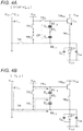
- FIG. 48 is a conceptual diagram illustrating a display device according to a first modified example.
- FIG. 49 is a schematic timing chart illustrating the operation of the display device according to the first modified example, more specifically, the operation of the (n, m)th display element of the display device.
- FIG. 50 is a conceptual diagram illustrating a display device according to a second modified example.
- FIGS. 51A and 51B show outside drawings of a lens-interchangeable single-lens reflex type digital still camera, FIG. 51A is a front view thereof, and FIG. 51B is a rear view thereof.
- a drive unit can be configured to scan display elements of a display unit consecutively, and to perform the operation of holding, in a first capacitor, a voltage corresponding to a threshold voltage of a driving transistor in a part of a plurality of consecutive frames.
- the above-described operation may be performed, for example, once every two frames, or once every five or ten frames. From the viewpoint of reducing the power consumption, it is preferable to reduce a frequency of frames in which the operation of holding a voltage corresponding to the threshold voltage of the driving transistor in the first capacitor is performed. Meanwhile, the voltage held in the first capacitor changes due to leakage or the like. Therefore, from the viewpoint of, for example, reducing uneven brightness, it is preferable to maintain a certain level of frequency. A level of frequency may be set as appropriate according to, for example, specifications of the display device.
- the operation of holding a voltage corresponding to the threshold voltage of the driving transistor in the first capacitor, and the operation of writing a video signal may be performed in some specific frame.
- the following operation may be performed: in some specific frame, for all display elements, performing only the operation of holding a voltage corresponding to the threshold voltage of the driving transistor in the first capacitor; and in the subsequent frame, performing the operation of writing a video signal.
- a video signal voltage that has been corrected to compensate for a change in voltage of the first capacitor may be written to a second capacitor, for example.
- the drive unit applies a reference voltage to the first node, and applies an initialization voltage to the second node and the third node, to set a voltage held by the capacitor unit so as to exceed the threshold voltage of the driving transistor, and subsequently applies the reference voltage to the first node, and applies the driving voltage to one source/drain region of the driving transistor in a state in which the second node and the third node electrically conduct with each other, so as to cause electric potentials of the second node and the third node to get close to a voltage obtained by subtracting the threshold voltage of the driving transistor from the reference voltage, consequently causing a voltage corresponding to the threshold voltage of the driving transistor to be held in the first capacitor.
- the display elements each further include a second switching transistor, a third switching transistor, and a fourth switching transistor;
- the reference voltage is applied to one source/drain region, and the other source/drain region is connected to the second node;
- one source/drain region is connected to the second node, and the other source/drain region is connected to the third node;
- the reference voltage is applied to one source/drain region, and the other source/drain region is connected to the first node;
- the reference voltage is applied to the first node by bringing the fourth switching transistor into the conducting state
- the second node and the third node are brought into the conducting state by bringing the third switching transistor into the conducting state.
- the initialization voltage is supplied from the data line through the first switching transistor.
- the initialization voltage may be supplied from the electric supply line through the driving transistor.
- the display elements each further include a fifth switching transistor
- the other source/drain region of the driving transistor may be connected to one end of the light-emitting unit through the fifth switching transistor.
- the display elements each further include a second switching transistor, a third switching transistor, and a fourth switching transistor;
- the initialization voltage is applied to one source/drain region, and the other source/drain region is connected to the second node;
- the reference voltage is applied to one source/drain region, and the other source/drain region is connected to the first node;
- the other source/drain region of the driving transistor is connected to one end of the light-emitting unit through the fourth switching transistor;
- the reference voltage is applied to the first node by bringing the third switching transistor into the conducting state
- the initialization voltage is applied to the first node by bringing the second switching transistor into the conducting state
- a conducting state/a non-conducting state of the second switching transistor are controlled by a control line in common with the first switching transistor.
- the drive unit applies a reference voltage to the first node, and applies an initialization voltage to the second node and the third node, to set a voltage held by the capacitor unit so as to exceed the threshold voltage of the driving transistor, and subsequently applies the reference voltage to the first node, and applies the driving voltage to one source/drain region of the driving transistor in a state in which the second node and the third node electrically conduct with each other, so as to cause electric potentials of the second node and the third node to get close to a voltage obtained by subtracting the threshold voltage of the driving transistor from the reference voltage, consequently causing a voltage corresponding to the threshold voltage of the driving transistor to be held in the first capacitor.
- the display elements each further include a second switching transistor, a third switching transistor, and a fourth switching transistor;
- the initialization voltage is applied to one source/drain region, and the other source/drain region is connected to the second node;
- the reference voltage is applied to one source/drain region, and the other source/drain region is connected to the first node;
- the other source/drain region of the driving transistor is connected to one end of the light-emitting unit through the fourth switching transistor;
- the reference voltage is applied to the first node by bringing the third switching transistor into the conducting state
- the initialization voltage is applied to the second node by bringing the second switching transistor into the conducting state
- a conducting state/a non-conducting state of the second switching transistor are controlled by a control line in common with the first switching transistor.
- the drive unit applies a reference voltage to the second node and the third node, and supplies a driving voltage from the electric supply line in a state in which the first node and one source/drain region of the driving transistor electrically conduct with each other, to set a voltage held by the capacitor unit so as to exceed a threshold voltage of the driving transistor, and subsequently
- the display elements each further include a second switching transistor, a third switching transistor, a fourth switching transistor, and a fifth switching transistor;
- the reference voltage is applied to one source/drain region, and the other source/drain region is connected to the second node;
- one source/drain region is connected to the second node, and the other source/drain region is connected to the third node;
- a connection between the first node and one source/drain region of the driving transistor is made through the fourth switching transistor;
- the reference voltage is applied to the second node and the third node by bringing the second switching transistor and the third switching transistor into the conducting state;
- the first node and one source/drain region of the driving transistor are brought into the conducting state by bringing the fourth switching transistor into the conducting state;
- connection between the electric supply line and the driving transistor is interrupted by bringing the fifth switching transistor into the non-conducting state.
- the display elements each further include a sixth switching transistor.
- the other source/drain region of the driving transistor is connected to one end of the light-emitting unit through the sixth switching transistor.
- the display elements each further include a second switching transistor, a third switching transistor, and a fourth switching transistor;
- the reference voltage is applied to one source/drain region, and the other source/drain region is connected to the second node;
- a connection between the first node and one source/drain region of the driving transistor is made through the third switching transistor;
- the reference voltage is supplied from the data line through the first switching transistor, and is applied to the first node, and the reference voltage is applied to the second node by bringing the second switching transistor into the conducting state;
- the first node and one source/drain region of the driving transistor are brought into the conducting state by bringing the third switching transistor into the conducting state;
- connection between the electric supply line and the driving transistor is interrupted by bringing the fourth switching transistor into the non-conducting state.
- the light-emitting unit may include a current-driven electro-optic element, the light emission brightness of which changes according to a value of a flowing current.
- An organic electroluminescent light-emitting unit, an LED light-emitting unit, a semiconductor laser light-emitting unit, and the like can be mentioned as the current-driven light-emitting unit.
- These light-emitting units can be configured by using a well-known material or method. From the viewpoint of configuring a flat-type display device, it is preferable that the light-emitting unit includes, above all, an organic electroluminescent light-emitting unit.
- the drive unit used in the present disclosure including the above-described various preferable configurations includes, for example, a circuit such as a data-line drive unit, a power supply unit, and a control-line drive unit. These can be configured by using a well-known circuit element or the like.
- the display device may be a so-called monochrome display configuration, or a color display configuration.
- one pixel may include a plurality of sub-pixels. More specifically, one pixel may include three sub-pixels that are a red light-emitting sub-pixel, a green light-emitting sub-pixel, and a blue light-emitting sub-pixel.
- one pixel may include a set of sub-pixels obtained by further adding one kind of or two or more kinds of sub-pixels to the above three kinds of sub-pixels (for example, a set of sub-pixels obtained by adding a sub-pixel that emits white light for improving brightness, a set of sub-pixels obtained by adding a sub-pixel that emits a complementary color for magnifying a color reproduction range, a set of sub-pixels obtained by adding a sub-pixel that emits yellow for magnifying a color reproduction range, and a set of sub-pixels obtained by adding sub-pixels that emit yellow and cyan for magnifying a color reproduction range).
- a set of sub-pixels obtained by adding a sub-pixel that emits white light for improving brightness for example, a set of sub-pixels obtained by adding a sub-pixel that emits white light for improving brightness, a set of sub-pixels obtained by adding a sub-pixel that emits a complementary color for magnifying a color reproduction range, a set of sub-pixel
- pixels (pixels) of the display device other than VGA (640, 480), S-VGA (800, 600), XGA (1024, 768), APRC (1152, 900), S-XGA (1280, 1024), U-XGA (1600, 1200), HD-TV (1920, 1080), and Q-XGA (2048, 1536), some image display resolutions such as (1920, 1035), (720, 480) and (1280, 960) can be presented. However, image display resolutions are not limited to these values.
- the display element that is included in the display unit is formed in a certain plane (for example, the display element is formed on a support base).
- the light-emitting unit is formed above the driving circuit that drives the light-emitting unit.
- the driving circuit that drives the light-emitting unit can be configured as a circuit that includes a transistor and a capacitor unit.
- a thin film transistor TFT
- the transistor may be an enhancement type transistor or a depletion type transistor.
- An n-channel transistor may be formed with a Lightly Doped Drain (LDD) structure.
- the LDD structure may be unsymmetrically formed. For example, a large current flows through the driving transistor when the display element emits light. Therefore, the LDD structure may be formed only in one source/drain region that becomes a drain region at the time of light emission.
- one source/drain region is used to mean a source/drain region connected to the power supply side.
- the source/drain regions can be configured not only from a conductive material such as polysilicon and amorphous silicon containing impurities, but also from a layer that includes metal, alloy, conductive particles, a layered structure thereof, and an organic material (conductive polymer).
- a conductive material such as polysilicon and amorphous silicon containing impurities
- Each capacitor that is included in the capacitor unit can be configured from a pair of electrodes, and a dielectric layer that is put between these electrodes.
- the transistor and the capacitor unit that are included in the driving circuit are formed in a certain plane (for example, the transistor and the capacitor unit are formed on the support base). For example, through the interlayer insulating layer, the light-emitting unit is formed above the transistor and the capacitor unit that are included in the driving circuit. It should be noted that a configuration in which a transistor is formed on a semiconductor substrate or the like may be employed.
- wiring lines such as a control line and a data line or an electric supply line are formed on a certain plane (for example, on the support base). These wiring lines can be regarded as a well-known configuration or structure.
- a constituent material of the support base or a constituent material of a substrate as described later other than a glass material such as high-strain point glass, soda glass (Na 2 O.CaO.SiO 2 ), borosilicate glass (Na 2 O.B 2 O 3 .SiO 2 ), forsterite (2MgO.SiO 2 ), and lead glass (Na 2 O.PbO.SiO 2 ), it is possible to present a flexible polymeric material, for example, a polymeric material, typified by polyether sulfone (PES), polyimide, polycarbonate (PC), and polyethylene terephthalate (PET).
- PES polyether sulfone
- PC polycarbonate
- PET polyethylene terephthalate
- a surface of the support base or a surface of the substrate may be provided with various coatings.
- the constituent material of the support base and the constituent material of the substrate may be the same, or may differ. If the support base and the substrate each including a flexible polymeric material are used, a flexible display device can be configured.
- a length (time length) of the horizontal axis indicating each time period is merely schematic, and thus does not indicate a ratio of the time length of each time period. The same applies to the vertical axis.
- waveform shapes in the timing chart are also schematic.
- the first embodiment relates to a display device, a display device driving method, and a display element according to the present disclosure.
- FIG. 1 is a conceptual diagram illustrating a display device according to the first embodiment.
- a display device 1 is provided with: a display unit 10 in which display elements 11 are arranged; and a drive unit 20 for driving the display unit 10 .
- the display elements 11 are arranged in a two-dimensional matrix form in a state in which the display elements 11 are connected to first to fifth control lines WS 1 to WS 5 each extending in a row direction (X direction in FIG. 1 ), and are connected to data lines DTL each extending in a column direction (Y direction in FIG. 1 ).
- FIG. 1 shows a connection line relationship for one of the display elements 11 , more specifically, for a (n, m)th display element 11 as described later.
- the display device 1 is provided with a data-line drive unit 21 , a power supply unit 22 , and a control-line drive unit 23 .
- the data-line drive unit 21 , the power supply unit 22 , and the control-line drive unit 23 constitute the drive unit 20 for driving the display unit 10 .
- control-line drive unit 23 Various signals are supplied from the control-line drive unit 23 to the first to fifth control lines WS 1 to WS 5 .
- a video signal voltage corresponding to the brightness of an image to be displayed is supplied to the data lines DTL.
- a driving voltage or the like is supplied from the power supply unit 22 to electric supply lines DS.
- the first to fifth control lines WS 1 to WS 5 are merely collectively referred to as “control lines”.
- a region (display region) in which the display unit 10 displays an image is constituted of the display elements 11 that are arranged in a two-dimensional matrix form formed by N pieces in the row direction, and M pieces in the column direction, that is to say, N ⁇ M pieces in total.
- the number of rows of the display elements 11 in the display region is M, and the number of the display elements 11 that constitute each row is N.
- the numbers of the first to fifth control lines WS 1 to WS 5 , and the number of the electric supply lines DS, are each M.
- FIG. 1 illustrates only the first to fifth control lines WS 1 m to WS 5 m , and the electric supply line DS m .
- the number of data lines DTL is N.
- the display element 11 includes: a current-driven light-emitting unit ELP; a capacitor unit CP including a first capacitor C S1 and a second capacitor C S2 ; an n-channel driving transistor TR Drv that causes a current corresponding to a voltage held by the capacitor unit CP to flow through the light-emitting unit ELP; and a first switching transistor TR 1 that writes a video signal voltage to the capacitor unit CP.
- the driving transistor TR Drv includes an n-channel TFT. The same applies to the other transistors.
- one end of the first capacitor C S1 is connected to a gate electrode of the driving transistor TR Drv to form a first node ND 1_G
- the other end of the first capacitor C S1 is connected to one end of the second capacitor C S2 to form a second node ND 2
- the other end of the second capacitor C S2 is connected to one end (anode electrode with which the light-emitting unit is provided) of the light-emitting unit ELP, and to the other source/drain region of the driving transistor TR Drv , to form a third node ND 3_S .
- one source/drain region is connected to the electric supply line DS, and the other source/drain region is connected to the light-emitting unit ELP through a fifth switching transistor TR 5 as described later.
- the first switching transistor TR 1 one source/drain region is connected to the data line DTL, and the other source/drain region is connected to the third node ND 3_S .
- the display elements 11 are each further provided with a second switching transistor TR 2 , a third switching transistor TR 3 , and a fourth switching transistor TR 4 .
- a reference voltage V ofs is applied to one source/drain region, and the other source/drain region is connected to the second node ND 2 .
- the third switching transistor TR 3 one source/drain region is connected to the second node ND 2 , and the other source/drain region is connected to the third node ND 3_S .
- the fourth switching transistor TR 4 the reference voltage V ofs is applied to one source/drain region, and the other source/drain region is connected to the first node ND 1_G .
- the display elements 11 are each further provided with a fifth switching transistor TR 5 .
- the other source/drain region of the driving transistor TR Drv is connected to one end of the light-emitting unit ELP through the fifth switching transistor TR 5 .
- the driving transistor TR Drv , the capacitor unit CP, and the first to fifth switching transistors TR 1 to TR 5 described above constitute a driving circuit 12 for driving the light-emitting unit ELP.
- Gate electrodes of the first to fifth switching transistors TR 1 to TR 5 are connected to the first to fifth control lines WS 1 to WS 5 respectively. Conducting state/non-conducting state of the first to fifth switching transistors TR 1 to TR 5 are controlled by a signal from the control-line drive unit 23 .
- the capacitor unit CP is used to hold a voltage of the gate electrode (so-called a voltage between a gate and a source) with respect to a source region of the driving transistor TR Drv .
- the “source region” means a source/drain region on the side that functions as a “source region” when the light-emitting unit ELP emits light.
- one source/drain region (the side connected to the electric supply line DS in FIG. 1 ) of the driving transistor TR Drv functions as a drain region
- the other source/drain region (the one end side of the light-emitting unit ELP) functions as a source region.
- the display device 1 is, for example, a monochrome display device, and one display element 11 forms one pixel.
- the display device 1 is line-sequentially scanned on a row basis by a control signal from the control-line drive unit 23 .
- the display element 11 located at the m-th row and the n-th column is referred to as the (n, m)th display element 11 or the (n, m)th pixel.
- a scanning period (horizontal scanning period) that is assigned to the display elements 11 in the m-th row is represented by reference numeral H m .
- a scanning period in a frame immediately before a frame to which the scanning period H m belongs is represented by reference numeral H′
- a scanning period in a frame immediately after a frame to which the scanning period H m belongs is represented by reference numeral H′′.
- the display elements 11 that form respective N pieces of pixels arranged in the m-th row are concurrently driven.
- the timing of light-emission/non-light emission is controlled for each row to which the display elements 11 belong.
- a display frame rate of the display device 1 is represented as FR (times/sec)
- a scanning period per row is less than (1/FR) ⁇ (1/M) seconds.
- a video signal D Sig representing gradation, and corresponding to an image to be displayed, is input into the display device 1 from, for example, a device that is not illustrated.
- the video signal D Sig is a digital signal based on the number of gradation bits such as 8 bits, 16 bits and 24 bits.
- a video signal corresponding to the (n, m)th display element 11 is represented as D Sig(n, m) .
- the data-line drive unit 21 generates a voltage corresponding to a value of the video signal D Sig , and supplies the voltage to the data line DTL.
- a video signal voltage corresponding to the video signal D Sig is represented as V Sig .
- the video signal voltage V Sig indicates corresponding to, for example, the (n, m)th display element 11
- the video signal voltage V Sig is represented as a video signal voltage V Sig(n, m) or a video signal voltage V Sig_m .
- the data-line drive unit 21 supplies an initialization voltage V ini and the video signal voltage V Sig to the data line DTL.
- the power supply unit 22 supplies a driving voltage V ccp to the electric supply line DS.
- the light-emitting unit ELP is a current-driven electro-optic element, the light emission brightness of which changes according to a value of a flowing current. More specifically, the light-emitting unit ELP includes an organic electroluminescent element.
- the light-emitting unit ELP has a well-known configuration or structure, and includes an anode electrode, a positive hole transport layer, a light-emitting layer, an electron transport layer, a cathode electrode, and the like.
- a voltage V cath (for example, 0 [V]) is applied to the other end (more specifically, the cathode electrode) of the light-emitting unit ELP from a common electric supply line. It is assumed that a threshold voltage required for light emission of the light-emitting unit ELP is V th-EL . When a voltage that is higher than or equal to V th-EL is applied between the anode electrode and the cathode electrode of the light-emitting unit ELP, the light-emitting unit ELP emits light.
- Reference numeral C EL represents a capacitance of the light-emitting unit ELP.
- an auxiliary capacitor C Sub that is connected to the light-emitting unit ELP in parallel has only to be provided.
- the explanation below is made on the assumption that the auxiliary capacitor C Sub is provided. However, the explanation is merely an example.
- the auxiliary capacitor C Sub may be omitted.
- FIG. 2 is a schematic partial cross-sectional view illustrating a part including a display element in the display unit.
- the transistors and the capacitor units are formed on a support base 31 , and the light-emitting unit ELP is formed above the transistors and the capacitor units through, for example, an interlayer insulating layer 50 .
- the unillustrated fifth switching transistor TR 5 and contact holes the other source/drain region of the driving transistor TR Drv is connected to the anode electrode with which the light-emitting unit ELP is provided.
- FIG. 2 Illustrates only the driving transistor TR Drv . The other transistors are hidden and do not appear.
- the driving transistor TR D includes a gate electrode 41 , a gate insulating layer 42 , one source/drain region 45 A that is provided in a semiconductor layer 43 , the other source/drain region 45 B, and a channel-forming region 44 that corresponds to a part of the semiconductor layer 43 between the one source/drain region 45 A and the other source/drain region 45 B.
- the first capacitor C S1 and the second capacitor C S2 that constitute the capacitor unit CP each include a pair of electrodes that sandwiches a dielectric layer including an extending part of the gate insulating layer 42 .
- the second capacitor C S2 includes one electrode 46 , the dielectric layer including the extending part of the gate insulating layer 42 , and the other electrode 47 .
- the second capacitor C S2 is hidden and does not appear.
- the gate electrode 41 , a part of the gate insulating layer 42 , and the one electrode 46 that constitutes the capacitor unit CP are formed on the support base 31 .
- the one source/drain region 45 A of the driving transistor TR Drv is connected to a wiring line 48 (corresponding to the electric supply line DS).
- the driving transistor TR Drv , the capacitor unit CP, and the like are covered with the interlayer insulating layer 50 .
- the light-emitting unit ELP that includes the anode electrode 61 , the positive hole transport layer, the light-emitting layer, the electron transport layer, and the cathode electrode 63 is provided on the interlayer insulating layer 50 .
- the positive hole transport layer, the light-emitting layer, and the electron transport layer are illustrated as one layer 62 in the figure.
- a second interlayer insulating layer 64 is provided on a part of the interlayer insulating layer 50 , the part not being provided with the light-emitting unit ELP.
- a transparent substrate 32 is arranged on the second interlayer insulating layer 64 and on the cathode electrode 63 . Light emitted in the light-emitting layer passes through the substrate 32 , and is then emitted to the outside.
- the cathode electrode 63 is connected to a wiring line 49 (corresponding to the common electric supply line that supplies the voltage V cath ) provided on the extending part of the gate insulating layer 42 .
- a voltage of the driving transistor TR Drv shown in FIG. 1 is set so as to operate in a saturation region in a light emitting state of the display element 11 , and is driven so as to cause a drain current I ds to flow according to the following equation (1).
- one source/drain region of the driving transistor TR Drv functions as a drain region
- the other source/drain region functions as a source region.
- V gs Gate electrode voltage (voltage between the gate and the source) for the source region
- This drain current I ds flows through the light-emitting unit ELP, which causes the light-emitting unit ELP of the display element 11 to emit light. Moreover, light intensity of the light-emitting unit ELP while the drain current I ds flows is controlled on the basis of a value of this drain current I ds .
- the display device 1 has been outlined as above.
- the above explanation is basically similar to those of the display devices in the other embodiments as described later. It should be noted that, for example, a difference in circuit configuration between the display elements will be described in detail in the explanation of each embodiment.
- FIG. 3 is a schematic timing chart illustrating the operation of the display device according to the first embodiment, more specifically, the operation of the (n, m)th display element of the display device.
- FIGS. 4A, 4B, 5A, 5B, 6A, 6B, 7A, 7B, 8A , and 8 B are drawings each schematically illustrating conducting state/non-conducting state and the like of each transistor that is included in a driving circuit of the display element of the display device according to the first embodiment.
- the drive unit 20 in a state in which a voltage corresponding to the threshold voltage V th of the driving transistor TR Drv is held by the first capacitor C S1 , the drive unit 20 writes the video signal voltage V Sig to the second capacitor C S2 through the first switching transistor TR 1 in a conducting state.
- the drive unit 20 successively scans the display elements 11 of the display unit 10 , and in a part of a plurality of consecutive frames, performs the operation of causing a voltage corresponding to the threshold voltage V th of the driving transistor TR Drv to be held in the first capacitor C S1 .
- the drive unit 20 applies the reference voltage V ofs to the first node ND 1_G , and applies the initialization voltage V ini to the second node ND 2 and the third node ND 3_S , thereby setting the voltage held by the capacitor unit CP so as to exceed the threshold voltage V th of the driving transistor TR Drv .
- the drive unit 20 applies the reference voltage V ofs to the first node ND 1_G , and applies the driving voltage V ccp to one source/drain region of the driving transistor TR Drv in a state in which the second node ND 2 and the third node ND 3_S electrically conduct with each other, so as to cause electric potentials of the second node ND 2 and the third node ND 3_S to get close to a voltage obtained by subtracting the threshold voltage V th of the driving transistor TR Drv from the reference voltage V ofs , thereby causing a voltage corresponding to the threshold voltage V th of the driving transistor TR Drv to be held in the first capacitor C S1 .
- the initialization voltage V ini is supplied from the data line DTL through the first switching transistor TR 1 .
- V ini Initialization voltage . . . ⁇ 3 V
- V ofs Reference voltage . . . 0 V
- V ccp Driving voltage for causing a current to flow through the light-emitting unit ELP . . . 15 V
- V Sig Video signal voltage . . . ⁇ 2 V to 0 V
- V th Threshold voltage of the driving transistor TR Drv . . . 1 V
- V cath Voltage applied to the cathode electrode of the light-emitting unit ELP . . . 0 V
- V th-EL Threshold voltage of the light-emitting unit ELP . . . 2 V
- This time period is before the [time period H′ m ⁇ 3 ] shown in FIG. 3 , and is a time period during which the (n, m)th display element 11 continues light emission after the completion of various processings last time.
- the fifth switching transistor TR 5 is in a conducting state, and the first to fourth switching transistors TR 1 to TR 4 are in a non-conducting state.
- the first to fourth control lines WS 1 m to WS 4 m are at a low level, and the fifth control line WS 5 m is at a high level.
- the drain current I ds represented by the above-described equation (1) flows through the light-emitting unit ELP, and thus the light-emitting unit ELP is in a light emitting state.
- Initialization processing is performed during this time period.
- the voltage held by the capacitor unit CP is set so as to exceed the threshold voltage V th of the driving transistor TR Drv .
- the fifth control line WS 5 m is switched to a low level.
- the fifth switching transistor TR 5 is in a non-conducting state.
- the driving transistor TR Drv and the light-emitting unit ELP are electrically separated from each other, and therefore the light-emitting unit ELP switches off the light.
- the first control line WS 1 m , the third control line WS 3 m , and the fourth control line WS 4 m are switched to a high level.
- the first switching transistor TR 1 , the third switching transistor TR 3 , and the fourth switching transistor TR 4 are in a conducting state.
- the second control line WS 2 m maintains a previous state, and therefore the second switching transistor TR 2 is in a non-conducting state.
- the reference voltage V ofs is applied to the first node ND 1_G through the fourth switching transistor TR 4 in the conducting state.
- the initialization voltage V ini is applied to the third node ND 3_S from the data line DTL through the first switching transistor TR 1 in the conducting state.
- the third switching transistor TR 3 is in the conducting state, and therefore the initialization voltage V ini is also applied to the second node ND 2 from the data line DTL.
- the voltage held by the capacitor unit CP becomes (V ofs ⁇ V ini ), and exceeds the threshold voltage V th of the driving transistor TR Drv .
- Threshold voltage cancel processing is performed during this time period.
- the reference voltage V ofs to the first node ND 1_G
- the driving voltage V ccp to one source/drain region of the driving transistor TR Drv in a state in which the second node ND 2 and the third node ND 3_S electrically conduct with each other
- electric potentials of the second node ND 2 and the third node ND 3_S are caused to get close to a voltage obtained by subtracting the threshold voltage V th of the driving transistor TR Drv from the reference voltage V ofs .
- the first control line WS 1 m is switched to a low level, and the fifth control line WS 5 m is switched to a high level.
- the other control lines maintain the previous state.
- the reference voltage V ofs is applied to the first node ND 1_G through the fourth switching transistor TR 4 .
- the second node ND 2 and the third node ND 3_S are in a conducting state through the third switching transistor TR 3 .
- the voltage held by the capacitor unit CP exceeds the threshold voltage V th of the driving transistor TR Drv , and therefore, through the driving transistor TR Drv , a current from the electric supply line DS flows through the third node ND 3_S .
- the electric potential of the third node ND 3_S increases toward an electric potential obtained by subtracting the threshold voltage V th of the driving transistor TR Drv from the reference voltage V ofs .
- the electric potential of the second node ND 2 that is in a conducting state with the third node ND 3_S also similarly increases (refer to FIG. 5A ).
- the explanation is made on the assumption that the driving transistor TR Drv is already in the non-conducting state during this time period.
- the present disclosure is not limited to this.
- a mode may be employed in which the time period ends before the electric potential difference between the gate electrode of the driving transistor TR Drv and the other source/drain region reaches V th .
- This time period is a time period immediately before performing the next write processing, and a time period for waiting for writing.
- the third control line WS 3 m , the fourth control line WS 4 m , and the fifth control line WS 5 m are switched to a low level.
- the third switching transistor TR 3 , the fourth switching transistor TR 4 , and the fifth switching transistor TR 5 enter the non-conducting state.
- the first control line WS 1 m and the second control line WS 2 m maintain the previous state.
- the first to fifth switching transistors TR 1 to TR 5 are in the non-conducting state.
- a video signal voltage V Sig_m is supplied to the data line DTL n in accordance with this time period.
- the video signal voltage V Sig_m is written to the second capacitor C S2 through the first switching transistor TR 1 in the conducting state.
- first control line WS 1 m and the second control line WS 2 m are switched to a high level.
- the other control lines maintain the previous state.
- the first switching transistor TR 1 and the second switching transistor TR 2 enter the conducting state.
- the other switching transistors are in the non-conducting state.
- an electric potential of the first node ND 1_G is V ofs
- an electric potential of the second node ND 2 is (V ofs ⁇ V th )
- the voltage V th is held in the first capacitor C S1 .
- the second switching transistor TR 2 enters the conducting state
- the reference voltage V ofs is applied to the second node ND 2 . Therefore, the electric potential of the second node ND 2 changes from (V ofs ⁇ V th ) to V ofs .
- the fourth switching transistor TR 4 is in the non-conducting state.
- the first capacitor C S1 maintains the previous state in which the voltage V th is held. Therefore, the electric potential of the first node ND 1_G becomes (V ofs +V th ) from V ofs .
- the video signal voltage V Sig_m is applied to the third node ND 3_S through the first switching transistor TR 1 in the conducting state.
- the reference voltage V ofs is applied to the second node ND 2 , and therefore a voltage, for example, (V ofs ⁇ V Sig_m ), is held in the second capacitor C S2 .
- the capacitor unit CP that includes the first capacitor C S1 and the second capacitor C S2 holds a voltage, for example, (V th +V ofs ⁇ V Sig_m ).
- a light emission period ranges from this time period until the starting period of a scanning period [time period: H m ⁇ 1 ] immediately before the scanning period H′′ m in the m-th row in the next frame.
- the first control line WS 1 m and the second control line WS 2 m are switched to a low level, and the fifth control line WS 5 m is switched to a high level.
- the fifth switching transistor TR 5 is in the conducting state, and the other switching transistors are in the non-conducting state.
- the fifth switching transistor TR 5 is in the conducting state, and therefore the voltage V gs between the gate and the source of the driving transistor TR Drv becomes a voltage (V th +V ofs ⁇ V Sig_m ) held by the capacitor unit CP.
- the driving voltage V ccp is applied to the source/drain region of one end of the driving transistor TR Drv , and therefore a current flows towards the light-emitting unit ELP through the driving transistor TR Drv and the fifth switching transistor TR 5 , which causes an electric potential of the third node ND 3_S to increase.
- a phenomenon similar to that of so-called a bootstrap circuit occurs in the gate electrode of the driving transistor TR Drv .
- the electric potential of the first node ND 1_G increases so as to maintain the voltage V gs between the gate and the source.
- the electric potential of the third node ND 3_S increases, and exceeds (V th-EL +V cath ), and therefore the light-emitting unit ELP starts light emission.
- a current flowing through the light-emitting unit ELP is the drain current I ds that flows from the drain region of the driving transistor TR Drv to the source region, and thus can be represented by equation (1).
- V gs is (V th +V ofs ⁇ V Sig_m ), and therefore the drain current I ds can be represented as the following equation (2).
- I ds k ⁇ ( V ofs ⁇ V Sig_m ) 2 (2)
- the current I ds flowing through the light-emitting unit ELP does not depend on the threshold voltage V th of the driving transistor TR Drv . In other words, since the influence exerted by the dispersion in threshold voltage V th of the driving transistor TR Drv of the display element 11 is canceled, the uneven brightness is reduced.
- This time period is a time period immediately before performing the next write processing.
- the voltage V th is already held in the first capacitor C S1 , and thus the operation corresponding to the above-described [time period: H′ m ⁇ 3 ] and [time period: H′ m ⁇ 2 ] is omitted.
- the second control line WS 2 m is switched to a high level, and the fifth control line WS 5 m is switched to a low level.
- the second switching transistor TR 2 is in the conducting state, and the other switching transistors are in the non-conducting state.
- the fifth switching transistor TR 5 is in the non-conducting state, and therefore a current does not flow through the light-emitting unit ELP. Therefore, the light-emitting unit ELP switches off the light.
- the reference voltage V ofs is applied to the second node ND 2 , and therefore the electric potential of the second node ND 2 decreases to become V ofs .
- the first node ND 1_G is in a floating state, and therefore the electric potential of the first node ND 1_G decreases according to the change in potential of the second node ND 2 .
- the first capacitor C S1 maintains a state in which the voltage V th is held.
- the electric potential of the third node ND 3_S further decreases from (V th-EL +V cath ) to some extent.
- the next frame starts from this time period.
- a video signal voltage V Sig_m is supplied to the data line DTL n in accordance with this time period.
- the video signal voltage V Sig_m is written to the second capacitor C S2 through the first switching transistor TR 1 in the conducting state.
- the first control line WS 1 m is switched to the high level.
- the other control lines maintain the previous state.
- the first switching transistor TR 1 and the second switching transistor TR 2 enter the conducting state.
- the other switching transistors are in the non-conducting state.
- the voltage V th is held in the first capacitor C S1 in a state in which the electric potential of the second node ND 2 is V ofs .
- the video signal voltage V Sig_m is applied to the third node ND 3_S through the first switching transistor TR 1 in the conducting state.
- the reference voltage V ofs is applied to the second node ND 2 , and therefore a voltage, for example, (V ofs ⁇ V Sig_m ), is held in the second capacitor C S2 .
- the capacitor unit CP that includes the first capacitor C S1 and the second capacitor C S2 holds a voltage, for example, (V th +V ofs ⁇ V Sig_m )
- the next frame light emission period starts from this time period.
- the first control line WS 1 m and the second control line WS 2 m are switched to a low level, and the fifth control line WS 5 m is switched to a high level.
- the fifth switching transistor TR 5 is in the conducting state, and the other switching transistors are in the non-conducting state.
- the specific operation is similar to the operation described in the above-described [time period: H m+1 ], and therefore the description thereof will be omitted.
- the operation described in the [time period: H′ m ⁇ 3 ] to the [time period: H′ m ⁇ 1 ] may be performed, for example, once every two frames, or once every five to ten frames. From the viewpoint of reducing the power consumption, it is preferable to reduce a frequency of frames in which the operation of holding a voltage corresponding to the threshold voltage V th of the driving transistor TR Drv in the first capacitor C S1 is performed. Meanwhile, the voltage held in the first capacitor C S1 changes due to leakage or the like. Therefore, from the viewpoint of, for example, reducing uneven brightness, it is preferable to maintain a certain level of frequency. A level of frequency may be set as appropriate according to, for example, specifications of the display device. The same applies to the other embodiments as described later.
- the second embodiment also relates to the display device, the display device driving method, and the display element according to the present disclosure.
- the initialization voltage V ini is supplied from the data line DTL n through the first switching transistor TR 1 .
- the initialization voltage V ini is supplied from the electric supply line DS through the driving transistor TR Drv .
- the second embodiment mainly differs from the first embodiment in the above point.
- the display device 1 has only to be replaced with the display device 2 in FIG. 1 .
- the operation of the drive unit differs from the operation in the first embodiment, a configuration thereof does not largely differ, and therefore the same reference numerals are used to denote components of the drive unit. The same applies to the other embodiments as described later.
- the data-line drive unit 21 supplies the video signal voltage V sig to the data line DTL n .
- the power supply unit 22 supplies the initialization voltage V ini and the driving voltage V ccp to the electric supply line DS.
- FIG. 9 is a schematic timing chart illustrating the operation of the display device according to the second embodiment, more specifically, the operation of the (n, m)th display element of the display device.
- FIGS. 10A and 10B show drawings each schematically illustrating conducting state/non-conducting state and the like of each transistor that is included in a driving circuit of the display element of the display device according to the second embodiment.
- This time period is before the [time period H′ m ⁇ 3 ] shown in FIG. 9 , and is a time period during which the (n, m)th display element 11 continues light emission after the completion of various processings last time.
- the driving voltage V ccp is supplied to the electric supply line DS m .
- the first to fourth switching transistors TR 1 to TR 4 are in the non-conducting state, and the fifth switching transistor TR 5 is in the conducting state.
- the first to fourth control lines WS 1 m to WS 4 m are at a low level, and the fifth control line WS 5 m is at a high level.
- the drain current I ds represented by the above-described equation (1) flows through the light-emitting unit ELP, and thus the light-emitting unit ELP is in a light emitting state.
- Initialization processing is performed during this time period.
- the voltage held by the capacitor unit CP is set so as to exceed the threshold voltage V th of the driving transistor TR Drv .
- the voltage supplied to the electric supply line DS m is switched to the initialization voltage V ini .
- the third control line WS 3 m and the fourth control line WS 4 m are switched to a high level.
- the other control lines maintain the previous state.
- the third to fifth switching transistors TR 3 to TR 5 are in the conducting state.
- the first switching transistor TR 1 and the second switching transistor TR 2 are in the non-conducting state.
- the second node ND 2 and the third node ND 3_S are in the conducting state through the third switching transistor TR 3 .
- the reference voltage V ofs is applied to the first node ND 1_G through the fourth switching transistor TR 4 .
- the fifth switching transistor TR 5 is in the conducting state.
- the voltage V gs between the gate and the source of the driving transistor TR Drv exceeds the threshold voltage V th . Therefore, the initialization voltage V ini is applied from the electric supply line DS m to the third node ND 3_S , and to the second node ND 2 that is in the conducting state with the third node ND 3_S , through the driving transistor TR Drv and the fifth switching transistor TR 5 .
- the voltage held by the capacitor unit CP becomes (V ofs ⁇ V ini ), and exceeds the threshold voltage V th of the driving transistor TR Drv .
- the electric potential of the third node ND 3_S does not exceed (V th-EL +V cath ), and therefore the light-emitting unit ELP switches off the light.
- the third embodiment also relates to the display device, the display device driving method, and the display element according to the present disclosure.
- the driving transistor TR Drv and the light-emitting unit ELP are connected through the switching transistor.
- the electric power is also consumed by a current flowing through the switching transistor, and therefore, from the viewpoint of attempting to achieve the electric power saving of the display device, it is preferable to directly connect the driving transistor TR Drv to the light-emitting unit ELP.
- the driving transistor TR Drv and the light-emitting unit ELP are configured to be directly connected to each other.
- FIG. 11 is a conceptual diagram illustrating a display device according to the third embodiment.
- a display device 3 is also provided with: the display unit 10 in which the display elements 11 are arranged; and the drive unit 20 for driving the display unit 10 .
- the data-line drive unit 21 supplies the video signal voltage V Sig to the data line DTL.
- the power supply unit 22 supplies the initialization voltage V ini and the driving voltage V ccp to the electric supply line DS.
- the capacitor unit CP, the driving transistor TR Drv , and the first switching transistor TR 1 in the display element 11 are configured in a similar manner to that described in the first embodiment, and therefore the description thereof will be omitted.
- the drive unit 20 applies the reference voltage V ofs to the first node ND 1_G , and applies the initialization voltage V ini to the second node ND 2 and the third node ND 3_S , thereby setting the voltage held by the capacitor unit CP so as to exceed the threshold voltage V th of the driving transistor TR Drv .
- the drive unit 20 applies the reference voltage V ofs to the first node ND 1_G , and applies the driving voltage V ccp to one source/drain region of the driving transistor TR Drv in a state in which the second node ND 2 and the third node ND 3_S electrically conduct with each other, so as to cause electric potentials of the second node ND 2 and the third node ND 3_S to get close to a voltage obtained by subtracting the threshold voltage V th of the driving transistor TR Drv from the reference voltage V ofs , thereby causing a voltage corresponding to the threshold voltage V th of the driving transistor TR Drv to be held in the first capacitor C S1 .
- the display element 11 is further provided with the second switching transistor TR 2 , the third switching transistor TR 3 , the fourth switching transistor TR 4 , and the fifth switching transistor TR 5 .
- a reference voltage V ofs is applied to one source/drain region, and the other source/drain region is connected to the second node ND 2 .
- the reference voltage V ofs is applied to one source/drain region, and the other source/drain region is connected to the first node ND 1_G .
- the second node ND 2 is connected to the other source/drain region of the driving transistor TR Drv and one end of the light-emitting unit ELP through the fourth switching transistor TR 4 .
- the third node ND 3_S is connected to the other source/drain region of the driving transistor TR Drv and one end of the light-emitting unit ELP through the fifth switching transistor TR 5 .
- the third switching transistor TR 3 is brought into the conducting state, which causes the reference voltage V ofs to be applied to the first node ND 1_G .
- the initialization voltage V ini is supplied from the electric supply line DS, and is applied to the second node ND 2 and the third node ND 3_S through the fourth switching transistor TR 4 and the fifth switching transistor TR 5 that are in the conducting state.
- FIG. 12 is a schematic timing chart illustrating the operation of the display device according to the third embodiment, more specifically, the operation of the (n, m)th display element of the display device.
- FIGS. 13A, 13B, 14A, 14B, 15A, 15B, 16A, 16B, 17A, and 17B are drawings each schematically illustrating conducting state/non-conducting state and the like of each transistor that is included in a driving circuit of the display element of the display device according to the third embodiment.
- This time period is before the [time period H′ m ⁇ 3 ] shown in FIG. 12 , and is a time period during which the (n, m)th display element 11 continues light emission after the completion of various processings last time.
- the driving voltage V ccp is supplied to the electric supply line DS m .
- the fifth switching transistor TR 5 is in the conducting state, and the other switching transistors are in the non-conducting state.
- the first to fourth control lines WS 1 m to WS 4 m are at a low level
- the fifth control line WS 5 m is at a high level.
- the drain current I ds represented by the above-described equation (1) flows through the light-emitting unit ELP, and thus the light-emitting unit ELP is in a light emitting state.
- Initialization processing is performed during this time period.
- the voltage held by the capacitor unit CP is set so as to exceed the threshold voltage V th of the driving transistor TR Drv .
- the voltage supplied to the electric supply line DS m is switched to the initialization voltage V ini .
- the third to fourth control lines WS 3 m to WS 4 m are switched to a high level.
- the other control lines maintain the previous state.
- the third to fifth switching transistors TR 3 to TR 5 are in the conducting state.
- the first switching transistor TR 1 and the second switching transistor TR 2 are in the non-conducting state.
- the reference voltage V ofs is applied to the first node ND 1_G through the third switching transistor TR 3 .
- the voltage V gs between the gate and the source of the driving transistor TR Drv exceeds the threshold voltage V th . Therefore, the initialization voltage V ini is applied from the electric supply line DS m to the second node ND 2 through the fourth switching transistor TR 4 .
- the initialization voltage V ini is applied from the electric supply line DS m to the third node ND 3_S through the fifth switching transistor TR 5 .
- the voltage held by the capacitor unit CP becomes (V ofs ⁇ V ini ), and exceeds the threshold voltage V th of the driving transistor TR Drv .
- the electric potential of the third node ND 3_S does not exceed (V th-EL +V cath ), and therefore the light-emitting unit ELP switches off the light.
- Threshold voltage cancel processing is performed during this time period.
- the reference voltage V ofs to the first node ND 1_G
- the driving voltage V ccp to one source/drain region of the driving transistor TR Drv in a state in which the second node ND 2 and the third node ND 3_S electrically conduct with each other
- electric potentials of the second node ND 2 and the third node ND 3_S are caused to get close to a voltage obtained by subtracting the threshold voltage V th of the driving transistor TR Drv from the reference voltage V ofs .
- the voltage supplied to the electric supply line DS m is switched to the driving voltage V ccp .
- the control lines maintain the previous state.
- the reference voltage V ofs is applied to the first node ND 1_G through the third switching transistor TR 3 .
- the voltage held by the capacitor unit CP exceeds the threshold voltage V th of the driving transistor TR Drv , and therefore, through the driving transistor TR Drv , a current from the electric supply line DS m flows through the third node ND 3_S .
- the electric potential of the third node ND 3_S increases toward an electric potential obtained by subtracting the threshold voltage V th of the driving transistor TR Drv from the reference voltage V ofs .
- the electric potential of the second node ND 2 that is in the conducting state with the third node ND 3_S also similarly increases (refer to FIG. 14A ).
- the explanation is made on the assumption that the driving transistor TR Drv is already in the non-conducting state during this time period.
- the present disclosure is not limited to this.
- a mode may be employed in which the time period ends before the electric potential difference between the gate electrode of the driving transistor TR Drv and the other source/drain region reaches V th .
- This time period is a time period immediately before performing the next write processing, and a time period for waiting for writing.
- the third control line WS 3 m and the fifth control line WS 5 m are switched to a low level.
- the other control lines maintain the previous state.
- the fourth switching transistor TR 4 is in the conducting state, and the other switching transistors are in the non-conducting state. If the driving transistor TR Drv is already in the non-conducting state in the [time period: H′ m ⁇ 2 ], electric potentials of the first node ND 1_G , the second node ND 2 and the third node ND 3_S do not substantially change (refer to FIG. 14B ). It should be noted that this time period may be omitted.
- a video signal voltage V Sig_m is supplied to the data line DTL n in accordance with this time period.
- the video signal voltage V Sig_m is written to the second capacitor C S2 through the first switching transistor TR 1 in the conducting state.
- first control line WS 1 m and the second control line WS 2 m are switched to a high level.
- the other control lines maintain the previous state.
- the first switching transistor TR 1 and the second switching transistor TR 2 enter the conducting state.
- the other switching transistors are in the non-conducting state.
- an electric potential of the first node ND 1_G is V ofs
- an electric potential of the second node ND 2 is (V ofs ⁇ V th )
- the voltage V th is held in the first capacitor C S1 .
- the second switching transistor TR 2 enters the conducting state
- the reference voltage V ofs is applied to the second node ND 2 . Therefore, the electric potential of the second node ND 2 changes from (V ofs ⁇ V th ) to V ofs .
- the third switching transistor TR 3 is in the non-conducting state.
- the first capacitor C S1 maintains the previous state in which the voltage V th is held. Therefore, the electric potential of the first node ND 1_G becomes (V ofs +V th ) from V ofs .
- the video signal voltage V Sig_m is applied to the third node ND 3_S through the first switching transistor TR 1 in the conducting state.
- the reference voltage V ofs is applied to the second node ND 2 , and therefore a voltage, for example, (V ofs ⁇ V Sig_m ), is held in the second capacitor C S2 .
- the capacitor unit CP that includes the first capacitor C S1 and the second capacitor C S2 holds a voltage, for example, (V th +V ofs ⁇ V Sig_m ).
- a light emission period ranges from this time period until the starting period of a scanning period [time period: H m ⁇ 1 ] immediately before the scanning period H′′ m in the m-th row in the next frame.
- the first control line WS 1 m , the second control line WS 2 m , and the fourth control line WS 4 m are switched to a low level, and the fifth control line WS 5 m is switched to a high level.
- the third control line WS 3 m maintains the previous state.
- the fifth switching transistor TR 5 is in the conducting state, and the other switching transistors are in the non-conducting state.
- the fifth switching transistor TR 5 is in the conducting state, and therefore the voltage V gs between the gate and the source of the driving transistor TR Drv becomes a voltage (V th +V ofs ⁇ V Sig_m ) held by the capacitor unit CP.
- the driving voltage V ccp is applied to the source/drain region of one end of the driving transistor TR Drv , and therefore a current flows towards the light-emitting unit ELP through the driving transistor TR Drv , which causes an electric potential of the third node ND 3_S to increase.
- a phenomenon similar to that of so-called a bootstrap circuit occurs in the gate electrode of the driving transistor TR Drv .
- the electric potential of the first node ND 1_G increases so as to maintain the voltage V gs between the gate and the source.
- the electric potential of the third node ND 3_S increases, and exceeds (V th-EL +V cath ), and therefore the light-emitting unit ELP starts light emission.
- the current I ds flowing through the light-emitting unit ELP is represented by the above-described equation (2), and therefore does not depend on the threshold voltage V th of the driving transistor TR Dr v. In other words, since the influence exerted by the dispersion in threshold voltage V th of the driving transistor TR Drv of the display element 11 is canceled, the uneven brightness is reduced.
- This time period is a time period immediately before performing the next write processing.
- the voltage V th is already held in the first capacitor C S1 , and thus the operation corresponding to the above-described [time period: H′ m ⁇ 3 ] and [time period: H′ m ⁇ 2 ] is omitted.
- the second control line WS 2 m is switched to a high level, and the fifth control line WS 5 m is switched to a low level.
- the second switching transistor TR 2 is in the conducting state, and the other switching transistors are in the non-conducting state.
- the reference voltage V ofs is applied to the second node ND 2 , and therefore the electric potential of the second node ND 2 decreases to become V ofs .
- the first node ND 1_G and the third node ND 3_S are in the floating state, and therefore these electric potentials also decrease according to the change in potential of the second node ND 2 .
- the first capacitor C S1 maintains a state in which the voltage V th is held.
- the next frame starts from this time period.
- a video signal voltage V Sig_m is supplied to the data line DTL n in accordance with this time period.
- the video signal voltage V Sig_m is written to the second capacitor C S2 through the first switching transistor TR 1 in the conducting state.
- the first control line WS 1 m is switched to the high level.
- the other control lines maintain the previous state.
- the first switching transistor TR 1 and the second switching transistor TR 2 are in the conducting state.
- the other switching transistors are in the non-conducting state.
- the voltage V th is held in the first capacitor C S1 in a state in which the electric potential of the second node ND 2 is V ofs .
- the video signal voltage V Sig_m is applied to the third node ND 3_S through the first switching transistor TR 1 in the conducting state.
- the reference voltage V ofs is applied to the second node ND 2 , and therefore a voltage, for example, (V ofs ⁇ V Sig_m ), is held in the second capacitor C S2 .
- the capacitor unit CP that includes the first capacitor C S1 and the second capacitor C S2 holds a voltage, for example, (V th +V ofs ⁇ V Sig_m )
- the next frame light emission period starts from this time period.
- the first control line WS 1 m and the second control line WS 2 m are switched to a low level, and the fifth control line WS 5 m is switched to a high level.
- the fifth switching transistor TR 5 is in the conducting state, and the other switching transistors are in the non-conducting state.
- the specific operation is similar to the operation described in the above-described [time period: H m+1 ], and therefore the description thereof will be omitted.
- the third embodiment if the operation of holding the threshold voltage V th in the first capacitor C S1 is performed in a certain frame, this operation can be omitted in a subsequent frame. Therefore, the power consumption can be further reduced while canceling the influence exerted by the dispersion in threshold voltage V th of the driving transistor TR Drv .
- the fourth embodiment also relates to the display device, the display device driving method, and the display element according to the present disclosure.
- the configuration of the display device becomes more complicated with the increase in the number of transistors that constitute the display element, and in the number of control lines. From the viewpoint of the electric power saving, cost reduction, or the like, it is preferable to reduce the number of transistors that constitute the display element. In addition, it is preferable to commonalize the control lines for controlling the transistors. In the fourth embodiment, the number of transistors and the number of control lines decrease in comparison with the first to third embodiments. In particular, the control lines are partially commonalized, and the second control line WS 2 is omitted.
- FIG. 18 is a conceptual diagram illustrating a display device according to the fourth embodiment.
- a display device 4 is also provided with: the display unit 10 in which the display elements 11 are arranged; and the drive unit 20 for driving the display unit 10 .
- the data-line drive unit 21 supplies the video signal voltage V sig and the initialization voltage V ini to the data line DTL.
- the power supply unit 22 supplies a driving voltage V ccp to the electric supply line DS.
- the capacitor unit CP, the driving transistor TR Drv , and the first switching transistor TR 1 in the display element 11 are configured in a similar manner to that described in the first embodiment, and therefore the description thereof will be omitted.
- the drive unit 20 applies the reference voltage V ofs to the first node ND 1_G , and applies the initialization voltage V ini to the second node ND 2 and the third node ND 3_S , thereby setting the voltage held by the capacitor unit CP so as to exceed the threshold voltage V th of the driving transistor TR Drv .
- the drive unit 20 applies the driving voltage V ccp to one source/drain region of the driving transistor TR Drv in a state in which the reference voltage V ofs is applied to the first node ND 1_G , so as to cause the electric potential of the third node ND 3_S to get close to a voltage obtained by subtracting the threshold voltage V th of the driving transistor TR Drv from the reference voltage V ofs , thereby causing a voltage corresponding to the threshold voltage V th of the driving transistor TR Drv to be held in the first capacitor C S1 .
- the display elements 11 are each further provided with the second switching transistor TR 2 , the third switching transistor TR 3 , and the fourth switching transistor TR 4 .
- the initialization voltage V ini is applied to one source/drain region, and the other source/drain region is connected to the second node ND 2 .
- the third switching transistor TR 3 the reference voltage V ofs is applied to one source/drain region, and the other source/drain region is connected to the first node ND 1_G .
- the other source/drain region of the driving transistor TR Drv is connected to one end of the light-emitting unit ELP through the fourth switching transistor TR 4 .
- the third switching transistor TR 3 is brought into the conducting state, which causes the reference voltage V ofs to be applied to the first node ND 1_G .
- the second switching transistor TR 2 is brought into the conducting state, which causes the initialization voltage V ini to be applied to the second node ND 2_G .
- the conducting state/non-conducting state of the second switching transistor TR 2 is controlled by a control line in common with the first switching transistor TR 1 , that is to say, the first control line WS 1 .
- FIG. 19 is a schematic timing chart illustrating the operation of the display device according to the fourth embodiment, more specifically, the operation of the (n, m)th display element of the display device.
- FIGS. 20A, 20B, 21A, 21B, 22A, 22B, 23, 23B, 24A, and 24B are drawings each schematically illustrating conducting state/non-conducting state and the like of each transistor that is included in a driving circuit of the display element of the display device according to the fourth embodiment.
- This time period is before the [time period H′ m ⁇ 3 ] shown in FIG. 19 , and is a time period during which the (n, m)th display element 11 continues light emission after the completion of various processings last time.
- the driving voltage V ccp is supplied to the electric supply line DS m .
- the first to third switching transistors TR 1 to TR 3 are in the non-conducting state.
- the fourth switching transistor TR 4 is in the conducting state.
- the first control line WS 1 m and the third control line WS 3 m are at a low level.
- the fourth control line WS 4 m is at a high level.
- the drain current I ds represented by the above-described equation (1) flows through the light-emitting unit ELP, and thus the light-emitting unit ELP is in a light emitting state.
- Initialization processing is performed during this time period.
- the voltage held by the capacitor unit CP is set so as to exceed the threshold voltage V th of the driving transistor TR Drv .
- the initialization voltage V ini is supplied to the data line DTL n .
- the first control line WS 1 m and the third control line WS 3 m are switched to a high level, and the fourth control line WS 4 m is switched to a low level.
- the first to third switching transistors TR 1 to TR 3 are in the conducting state.
- the fourth switching transistor TR 4 is in the non-conducting state.
- the fourth switching transistor TR 4 is in the non-conducting state, and therefore a current flowing through the driving transistor TR Drv does not flow through the light-emitting unit ELP.
- the reference voltage V ofs is applied to the first node ND 1_G through the third switching transistor TR 3 .
- the initialization voltage V ini is applied to the second node ND 2 through the second switching transistor TR 2 .
- the initialization voltage V ini is applied from the data line DTL n to the third node ND 3_S through the first switching transistor TR 1 .
- the voltage held by the capacitor unit CP becomes (V ofs ⁇ V ini ), and exceeds the threshold voltage V th of the driving transistor TR Drv .
- the electric potential of the third node ND 3_S does not exceed (V th-EL +V cath ), and therefore the light-emitting unit ELP maintains a non-lighting state.
- Threshold voltage cancel processing is performed during this time period.
- the driving voltage V ccp is applied to one source/drain region of the driving transistor TR Drv in a state in which the reference voltage V ofs is applied to the first node ND 1_G , so as to cause the electric potential of the third node ND 3_S to get close to a voltage obtained by subtracting the threshold voltage V th of the driving transistor TR Drv from the reference voltage V ofs , thereby causing a voltage corresponding to the threshold voltage V th of the driving transistor TR Drv to be held in the first capacitor C S1 .
- the first control line WS 1 m is switched to a low level, and the fourth control line WS 4 m is switched to a high level.
- the third control line WS 3 m maintains the previous state.
- the third switching transistor TR 3 and the fourth switching transistor TR 4 are in the conducting state.
- the first switching transistor TR 1 and the second switching transistor TR 2 are in the non-conducting state.
- the reference voltage V ofs is applied to the first node ND 1_G through the third switching transistor TR 3 .
- the voltage held by the capacitor unit CP exceeds the threshold voltage V th of the driving transistor TR Drv , and therefore, through the driving transistor TR Drv , a current from the electric supply line DS m flows through the third node ND 3_S .
- the electric potential of the third node ND 3_S increases toward an electric potential obtained by subtracting the threshold voltage V th of the driving transistor TR Drv from the reference voltage V ofs .
- an electric potential difference between the gate electrode of the driving transistor TR Drv and the other source/drain region reaches V th , and the driving transistor TR Drv enters the non-conducting state (refer to FIG. 21B ).
- an electric potential difference between the first node ND 1_G and the third node ND 3_S becomes (V ofs ⁇ V th ).
- the electric potential of the first node ND 1_G is V ofs
- the electric potential of the third node ND 3_S is (V ofs ⁇ V th ).
- the explanation is made on the assumption that the driving transistor TR Drv is already in the non-conducting state during this time period.
- the present disclosure is not limited to this.
- a mode may be employed in which the time period ends before the electric potential difference between the gate electrode of the driving transistor TR Drv and the other source/drain region reaches V th .
- V th ′ V ofs ⁇ V ini ⁇ V ND2 (5)
- ⁇ V ND2 is a voltage determined according to V th . Therefore, a voltage corresponding to the threshold voltage V th is held in the second capacitor C S2 .
- This time period is a time period immediately before performing the next write processing, and a time period for waiting for writing.
- the third control line WS 3 m and the fourth control line WS 4 m are switched to a low level, and the first control line WS 1 m maintains the previous state.
- the first to fourth switching transistors TR 1 to TR 4 are in the non-conducting state. If the driving transistor TR Drv is already in the non-conducting state in the [time period: H′ m ⁇ 2 ], electric potentials of the first node ND 1_G , the second node ND 2 , and the third node ND 3_S do not substantially change. It should be noted that this time period may be omitted.
- a video signal voltage V Sig_m is supplied to the data line DTL n in accordance with this time period.
- the video signal voltage V Sig_m is written to the second capacitor C S2 through the first switching transistor TR 1 in the conducting state.
- the first control line WS 1 m is switched to the high level.
- the other control lines maintain the previous state.
- the first switching transistor TR 1 and the second switching transistor TR 2 are in the conducting state.
- the other switching transistors are in the non-conducting state.
- the electric potential of the first node ND 1_G is V ofs
- the electric potential of the third node ND 3_S is (V ofs ⁇ V th )
- the voltage V th ′ is held by the first capacitor C S1 .
- the second switching transistor TR 2 enters the conducting state
- the reference voltage V ofs is applied to the second node ND 2 . Therefore, the electric potential of the second node ND 2 changes from (V ofs ⁇ V th ′) to V ofs .
- the third switching transistor TR 3 is in the non-conducting state.
- the first capacitor C S1 maintains the previous state in which the voltage V th ′ is held. Therefore, the electric potential of the first node ND 1_G becomes (V ofs +V th ′) from V ofs .
- the video signal voltage V Sig_m is applied to the third node ND 3_S through the first switching transistor TR 1 in the conducting state.
- the reference voltage V ofs is applied to the second node ND 2 , and therefore a voltage, for example, (V ofs ⁇ V Sig_m ), is held in the second capacitor C S2 .
- the capacitor unit CP that includes the first capacitor C S1 and the second capacitor C S2 holds a voltage, for example, (V th ′+V ofs ⁇ V Sig_m ).
- a light emission period ranges from this time period until the starting period of a scanning period [time period: H m ⁇ 1 ] immediately before the scanning period H′′ m in the m-th row in the next frame.
- the first control line WS 1 m is switched to a low level, and the fourth control line WS 4 m is switched to a high level.
- the third control line WS 3 m maintains the previous state.
- the fourth switching transistor TR 4 is in the conducting state, and the other switching transistors are in the non-conducting state.
- the voltage V gs between the gate and the source of the driving transistor TR Dr v becomes a voltage (V th ′+V ofs ⁇ V Sig_m ) held by the capacitor unit CP.
- the driving voltage V ccp is applied to the source/drain region of one end of the driving transistor TR Drv , and therefore a current flows towards the light-emitting unit ELP through the driving transistor TR Drv , which causes an electric potential of the third node ND 3_S to increase.
- a phenomenon similar to that of so-called a bootstrap circuit occurs in the gate electrode of the driving transistor TR Drv .
- the electric potential of the first node ND 1_G increases so as to maintain the voltage V gs between the gate and the source.
- I ds k ⁇ ( V ofs ⁇ V Sig_m ⁇ ( V th ⁇ V th ′)) 2 (6)
- This time period is a time period immediately before performing the next write processing.
- the voltage V th ′ is already held in the first capacitor C S1 , and thus the operation corresponding to the above-described [time period: H′ m ⁇ 3 ] and [time period: H′ m ⁇ 2 ] is omitted.
- the fourth control line WS 4 m is switched to a low level.
- the other control lines maintain the previous state.
- the first to fourth switching transistors TR 1 to TR 4 are in the non-conducting state.
- the fourth switching transistor TR 4 is in the non-conducting state, and therefore a current flowing through the driving transistor TR Drv does not flow through the light-emitting unit ELP. Therefore, the light-emitting unit ELP switches off the light.
- the electric potential of the third node ND 3_S decreases to (V th-EL +V cath ).
- the first node ND 1_G and the second node ND 2_S are in the floating state, and therefore these electric potentials also decrease according to the change in potential of the third node ND 3_S .
- the first capacitor C S1 maintains a state in which the voltage V th ′ is held.
- the next frame starts from this time period.
- a video signal voltage V Sig_m is supplied to the data line DTL n in accordance with this time period.
- the video signal voltage V Sig_m is written to the second capacitor C S2 through the first switching transistor TR 1 in the conducting state.
- the first control line WS 1 m is switched to the high level.
- the other control lines maintain the previous state.
- the first switching transistor TR 1 and the second switching transistor TR 2 are in the conducting state.
- the other switching transistors are in the non-conducting state.
- the voltage V th ′ is held in the first capacitor C S1 .
- the video signal voltage V Sig_m is applied to the third node ND 3_S through the first switching transistor TR 1 in the conducting state.
- the reference voltage V ofs is applied to the second node ND 2 , and therefore a voltage, for example, (V ofs ⁇ V Sig_m ), is held in the second capacitor C S2 .
- the capacitor unit CP that includes the first capacitor C S1 and the second capacitor C S2 holds a voltage, for example, (V th ′+V ofs ⁇ V Sig_m ).
- the next frame light emission period starts from this time period.
- the first control line WS 1 m is switched to a low level, and the fourth control line WS 4 m is switched to a high level.
- the second control line WS 2 m maintains the previous state.
- the fourth switching transistor TR 4 is in the conducting state, and the other switching transistors are in the non-conducting state.
- the specific operation is similar to the operation described in the above-described [time period: H m+1 ], and therefore the description thereof will be omitted.
- the fourth embodiment if the operation of holding the threshold voltage V th in the first capacitor C S1 is performed in a certain frame, this operation can be omitted in a subsequent frame. Therefore, the power consumption can be further reduced while canceling the influence exerted by the dispersion in threshold voltage V th of the driving transistor TR Drv .
- the fourth embodiment is also suitable for achieving high definition of the display device.
- the fifth embodiment also relates to the display device, the display device driving method, and the display element according to the present disclosure.
- the first to fourth embodiments described above each have the configuration in which when a voltage is held in the first capacitor C S1 , the electric potential of the third node ND 3_S is caused to get close to a voltage obtained by subtracting the threshold voltage V th of the driving transistor TR Drv from the reference voltage V ofs .
- the fifth embodiment has a configuration in which when a voltage is held in the first capacitor C S1 , the electric potential of the first node ND 1_G is caused to get close to an electric potential obtained by adding the threshold voltage V th of the driving transistor TR Drv to the reference voltage V ofs .
- FIG. 25 is a conceptual diagram illustrating a display device according to the fifth embodiment.
- a display device 5 is also provided with: the display unit 10 in which the display elements 11 are arranged; and the drive unit 20 for driving the display unit 10 .
- the data-line drive unit 21 supplies the video signal voltage V sig to the data line DTL.
- the power supply unit 22 supplies a driving voltage V ccp to the electric supply line DS.
- the capacitor unit CP, the driving transistor TR Drv , and the first switching transistor TR 1 in the display element 11 are configured in a similar manner to that described in the first embodiment, and therefore the description thereof will be omitted.
- the drive unit 20 applies the reference voltage V ofs to the second node ND 2 and the third node ND 3_S , and supplies the driving voltage V ccp from the electric supply line DS in a state in which the first node ND 1_G and one source/drain region of the driving transistor TR Drv electrically conduct with each other, thereby setting the voltage held by the capacitor unit CP so as to exceed the threshold voltage V th of the driving transistor TR Drv .
- a connection between the electric supply line DS and the driving transistor TR Drv is interrupted in a state in which the reference voltage V ofs is applied to the second node ND 2 and the third node ND 3_S , so as to cause the electric potential of the first node ND 1_G to get close to an electric potential obtained by adding the threshold voltage V th of the driving transistor TR Drv to the reference voltage V ofs , thereby causing a voltage corresponding to the threshold voltage V th of the driving transistor TR Drv to be held in the first capacitor C S1 .
- the display element 11 is further provided with the second switching transistor TR 2 , the third switching transistor TR 3 , the fourth switching transistor TR 4 , and the fifth switching transistor TR 5 .
- a reference voltage V ofs is applied to one source/drain region, and the other source/drain region is connected to the second node ND 2 .
- the third switching transistor TR 3 one source/drain region is connected to the second node ND 2 , and the other source/drain region is connected to the third node ND 3_S .
- a connection between the first node ND 1_G and one source/drain region of the driving transistor TR Drv is made through the fourth switching transistor TR 4 .
- a connection between the electric supply line DS and one source/drain region of the driving transistor TR Drv is made through the fifth switching transistor TR 5 .
- the reference voltage V ofs is applied to the second node ND 2 and the third node ND 3_S by bringing the second switching transistor TR 2 and the third switching transistor TR 3 into the conducting state.
- the first node ND 1_G and one source/drain region of the driving transistor TR Drv are brought into the conducting state by bringing the fourth switching transistor TR 4 into the conducting state.
- the connection between the electric supply line DS and the driving transistor TR Drv is interrupted by bringing the fifth switching transistor TR 5 into the non-conducting state.
- FIG. 26 is a schematic timing chart illustrating the operation of the display device according to the fifth embodiment, more specifically, the operation of the (n, m)th display element of the display device.
- FIGS. 27A, 27B, 28A, 28B, 29A, 29B, 30A, 30B, 31A, and 31B are drawings each schematically illustrating conducting state/non-conducting state and the like of each transistor that is included in a driving circuit of the display element of the display device according to the fifth embodiment.
- This time period is before the [time period H′ m ⁇ 3 ] shown in FIG. 26 , and is a time period during which the (n, m)th display element 11 continues light emission after the completion of various processings last time.
- the driving voltage V ccp is supplied to the electric supply line DS m .
- the first to fourth switching transistors TR 1 to TR 4 are in the non-conducting state, and the fifth switching transistor TR 5 is in the conducting state.
- the first to fourth control lines WS 1 m to WS 4 m are at a low level, and the fifth control line WS 5 m is at a high level.
- the drain current I ds represented by the above-described equation (1) flows through the light-emitting unit ELP, and thus the light-emitting unit ELP is in a light emitting state.
- Initialization processing is performed during this time period.
- the reference voltage V ofs is applied to the second node ND 2 and the third node ND 3_S
- the driving voltage V ccp is supplied from the electric supply line DS m in a state in which the first node ND 1_G and one source/drain region of the driving transistor TR Drv electrically conduct with each other, thereby setting the voltage held by the capacitor unit CP so as to exceed the threshold voltage V th of the driving transistor TR Drv .
- the second to fourth control lines WS 2 m to WS 4 m are switched to a high level.
- the other control lines maintain the previous state.
- the second to fifth switching transistors TR 2 to TR 5 are in the conducting state.
- the first switching transistor TR 1 is in the non-conducting state.
- the second node ND 2 and the third node ND 3_S are in the conducting state through the third switching transistor TR 3 .
- the reference voltage V ofs is applied to the second node ND 2 and the third node ND 3_S through the second switching transistor TR 2 .
- the driving voltage V ccp is applied from the electric supply line DS m to the first node ND 1_G through the fourth switching transistor TR 4 . Therefore, the voltage held by the capacitor unit CP becomes (V ccp ⁇ V ofs ), and exceeds the threshold voltage V th of the driving transistor TR Drv .
- the driving voltage V ccp is applied from the electric supply line DS m to one end of the light-emitting unit ELP through the fifth switching transistor TR 5 and the driving transistor TR Drv . Therefore, it is also considered that the light-emitting unit ELP performs unintended light emission. However, one end of the light-emitting unit ELP is connected to the third node ND 3_S , and therefore a path of a through current is formed through the fifth switching transistor TR 5 , the driving transistor TR Drv , the third switching transistor TR 3 , and the second switching transistor TR 2 . Taking the threshold voltage V th-EL of the light-emitting unit ELP or the like into consideration, it is considered that a current generally flows through the path of the through current.
- Threshold voltage cancel processing is performed during this time period.
- the electric potential of the first node ND 1_G is caused to get close to an electric potential obtained by adding the threshold voltage V th of the driving transistor TR Drv to the reference voltage V ofs .
- the fifth control line WS 5 m is switched to a low level.
- the other control lines maintain the previous state.
- the second to fourth switching transistors TR 2 to TR 4 are in the conducting state.
- the first switching transistor TR 1 and the fifth switching transistor TR 5 are in the non-conducting state.
- the reference voltage V ofs is applied to the second node ND 2 through the second switching transistor TR 2 , and the reference voltage V ofs is applied to the third node ND 3_S through the second switching transistor TR 2 and the third switching transistor TR 3 .
- the fifth switching transistor TR 5 is in the non-conducting state, and therefore the electric supply line DS m is electrically isolated from one source/drain region of the driving transistor TR Drv .
- the voltage V gs between the gate and the source of the driving transistor TR Drv is the voltage (V ccp ⁇ V ofs ) held by the capacitor unit CP, and exceeds the threshold voltage V th .
- the first node ND 1_G and one source/drain region of the driving transistor TR Drv electrically conduct with each other by the fourth switching transistor TR 4 .
- a current flows from the first node ND 1_G through the driving transistor TR Drv , which causes the electric potential of the first node ND 1_G to decrease ( FIG. 28A ).
- the explanation is made on the assumption that the driving transistor TR Drv is already in the non-conducting state during this time period.
- the present disclosure is not limited to this.
- a mode may be employed in which the time period ends before the electric potential difference between the gate electrode of the driving transistor TR Drv and the other source/drain region reaches V th .
- This time period is a time period immediately before performing the next write processing, and a time period for waiting for writing.
- the third control line WS 3 m and the fourth control line WS 4 m are switched to a low level, and the other control lines maintain the previous state.
- the second switching transistor TR 2 is in the conducting state, and the first switching transistors TR 1 , the fourth switching transistor TR 4 , and the fifth switching transistor TR 5 are in the non-conducting state. If the driving transistor TR Drv is already in the non-conducting state in the [time period: H′ m ⁇ 2 ], electric potentials of the first node ND 1_G , the second node ND 2 , and the third node ND 3_S do not substantially change. It should be noted that this time period may be omitted.
- a video signal voltage V Sig_m is supplied to the data line DTL in accordance with this time period.
- the video signal voltage V Sig_m is written to the second capacitor C S2 through the first switching transistor TR 1 in the conducting state.
- the first control line WS 1 m is switched to the high level.
- the other control lines maintain the previous state.
- the first switching transistor TR 1 and the second switching transistor TR 2 are in the conducting state.
- the other switching transistors are in the non-conducting state.
- the electric potential of the first node ND 1 _G is (Vofs+ V th)
- the electric potential of the second node ND 2 is Vofs
- the voltage Vth is held in the first capacitor CS 1 .
- the reference voltage Vofs is applied to the second node ND 2 through the first switching transistor TR 1 .
- the video signal voltage VSig_m is applied to the third node ND 3 _S through the first switching transistor TR 1 .
- the reference voltage Vofs is applied to the second node ND 2 , and therefore a voltage, for example, (Vofs ⁇ VSig_m), is held in the second capacitor CS 2 .
- the capacitor unit CP that includes the first capacitor CS 1 and the second capacitor CS 2 holds a voltage, for example, (Vth+Vofs ⁇ VSig_m).
- a light emission period ranges from this time period until the starting period of a scanning period [time period: H m ⁇ 1 ] immediately before the scanning period H′′ m in the m-th row in the next frame.
- first control line WS 1 m and the second control line WS 2 m are switched to a low level, and the fifth control line WS 5 m is switched to a high level.
- the third control line WS 3 m and the fourth control line WS 4 m maintain the previous state.
- the fifth switching transistor TR 5 is in the conducting state, and the other switching transistors are in the non-conducting state.
- the voltage V gs between the gate and the source of the driving transistor TR Drv becomes a voltage (V th +V ofs ⁇ V Sig_m ) held by the capacitor unit CP.
- the driving voltage V ccp is applied to the source/drain region of one end of the driving transistor TR Drv , and therefore a current flows towards the light-emitting unit ELP through the driving transistor TR Drv , which causes an electric potential of the third node ND 3s to increase.
- a phenomenon similar to that of so-called a bootstrap circuit occurs in the gate electrode of the driving transistor TR Drv .
- the electric potential of the first node ND 1_G increases so as to maintain the voltage V gs between the gate and the source.
- the electric potential of the third node ND 3s increases, and exceeds (V th-EL +V cath ), and therefore the light-emitting unit ELP starts light emission.
- the current I ds flowing through the light-emitting unit ELP is represented by the above-described equation (2), and therefore does not depend on the threshold voltage V th of the driving transistor TR Drv . In other words, since the influence exerted by the dispersion in threshold voltage V th of the driving transistor TR Drv of the display element 11 is canceled, the uneven brightness is reduced.
- This time period is a time period immediately before performing the next write processing.
- the voltage V th is already held in the first capacitor C S1 , and thus the operation corresponding to the above-described [time period: H′ m ⁇ 3 ] and [time period: H′ m ⁇ 2 ] is omitted.
- the second control line WS 2 m is switched to a high level, and the fifth control line WS 5 m is switched to a low level.
- the other control lines maintain the previous state.
- the second switching transistor TR 2 is in the conducting state, and the other switching transistors are in the non-conducting state.
- the reference voltage V ofs is applied to the second node ND 2 , and therefore the electric potential of the second node ND 2 decreases to become V ofs .
- the first node ND 1_G is in a floating state, and therefore the electric potential of the first node ND 1_G decreases according to the change in potential of the second node ND 2 .
- the first capacitor C S1 maintains a state in which the voltage V th is held.
- the electric potential of the third node ND 3_S further decreases from (V th-EL +V cath ) to some extent.
- the next frame starts from this time period.
- a video signal voltage V Sig_m is supplied to the data line DTL n in accordance with this time period.
- the video signal voltage V Sig_m is written to the second capacitor C S2 through the first switching transistor TR 1 in the conducting state.
- the first control line WS 1 m is switched to the high level.
- the other control lines maintain the previous state.
- the first switching transistor TR 1 and the second switching transistor TR 2 are in the conducting state.
- the other switching transistors are in the non-conducting state.
- the voltage V th is held in the first capacitor C S1 in a state in which the electric potential of the second node ND 2 is V ofs .
- the video signal voltage V Sig_m is applied to the third node ND 3_S through the first switching transistor TR 1 in the conducting state.
- the reference voltage V ofs is applied to the second node ND 2 , and therefore a voltage, for example, (V ofs ⁇ V Sig_m ), is held in the second capacitor C S2 .
- the capacitor unit CP that includes the first capacitor C S1 and the second capacitor C S2 holds a voltage, for example, (V th +V ofs ⁇ V Sig_m ).
- the next frame light emission period starts from this time period.
- the first control line WS 1 m and the second control line WS 2 m are switched to a low level, and the fifth control line WS 5 m is switched to a high level.
- the fifth switching transistor TR 5 is in the conducting state, and the other switching transistors are in the non-conducting state.
- the specific operation is similar to the operation described in the above-described [time period: H m +], and therefore the description thereof will be omitted.
- the fifth embodiment if the operation of holding the threshold voltage V th in the first capacitor C S1 is performed in a certain frame, this operation can be omitted in a subsequent frame. Therefore, the power consumption can be further reduced while canceling the influence exerted by the dispersion in threshold voltage V th of the driving transistor TR Drv .
- the initialization voltage V ini as well as the reference voltage V ofs is required.
- the initialization voltage V ini is not required. Accordingly, the fifth embodiment also has an advantage of being capable of reducing kinds of voltages supplied by the drive unit.
- the sixth embodiment also relates to the display device, the display device driving method, and the display element according to the present disclosure.
- the sixth embodiment mainly differs from the fifth embodiment in the operation of the [time period: H′ m ⁇ 3 ]. More specifically, a transistor is controlled so as not to form a path of a through current.
- the display device 5 has only to be replaced with the display device 6 in FIG. 25 .
- the data-line drive unit 21 supplies the video signal voltage V sig to the data line DTL.
- the power supply unit 22 supplies a driving voltage V ccp to the electric supply line DS.
- FIG. 32 is a schematic timing chart illustrating the operation of the display device according to the sixth embodiment, more specifically, the operation of the (n, m)th display element of the display device.
- FIGS. 33A and 33B show drawings each schematically illustrating conducting state/non-conducting state and the like of each transistor that is included in a driving circuit of the display element of the display device according to the sixth embodiment.
- the first half of the initialization processing is performed during this time period.
- the second control line WS 2 m and the fourth control line WS 4 m are switched to a high level, and the other control lines maintain the previous state.
- the second switching transistor TR 2 and the fifth switching transistor TR 5 are in the conducting state.
- the other switching transistors are in the non-conducting state.
- the reference voltage V ofs is applied to the second node ND 2 through the second switching transistor TR 2 .
- the driving voltage V ccp is applied from the electric supply line DS m to the first node ND 1_G through the fourth switching transistor TR 4 .
- the driving voltage V ccp is applied from the electric supply line DS m to one end of the light-emitting unit ELP through the fifth switching transistor TR 5 and the driving transistor TR Drv .
- the latter half of the initialization processing and the threshold voltage cancel processing are performed during this time period.
- the third control line WS 3 m is switched to a high level, and the fifth control line WS 5 m is switched to a low level.
- the second to fourth switching transistors TR 2 to TR 4 are in the conducting state.
- the first switching transistor TR 1 and the fifth switching transistor TR 5 are in the non-conducting state.
- the reference voltage V ofs is applied to the third node ND 3_S through the second switching transistor TR 2 and the third switching transistor TR 3 .
- an electric potential of the first node ND 1_G is V cc p. Therefore, in the starting period of this time period, the voltage held by the capacitor unit CP becomes (V ofs ⁇ V ini ), and exceeds the threshold voltage V th of the driving transistor TR Drv .
- the reference voltage V ofs is applied to the second node ND 2 through the second switching transistor TR 2
- the reference voltage V ofs is applied to the third node ND 3_S through the second switching transistor TR 2 and the third switching transistor TR 3 .
- the fifth switching transistor TR 5 is in the non-conducting state, and therefore the electric supply line DS m is electrically isolated from one source/drain region of the driving transistor TR Drv .
- the voltage V gs between the gate and the source of the driving transistor TR Drv is the voltage (V ccp ⁇ V ofs ) held by the capacitor unit CP, and exceeds the threshold voltage V th .
- the first node ND 1_G and one source/drain region of the driving transistor TR Drv electrically conduct with each other by the fourth switching transistor TR 4 .
- the sixth embodiment also does not require the initialization voltage V ini , and therefore has the advantage of being capable of reducing kinds of voltages supplied by the drive unit. Further, the sixth embodiment also has the advantage of reducing a load of the element caused by the through current flowing through the transistor. It should be noted that since the contrast decreases due to unintended light emission, it is preferable that a time period during which the processing of the [time period: H′ m ⁇ 3 ] is performed be set to be short.
- the seventh embodiment also relates to the display device, the display device driving method, and the display element according to the present disclosure.
- the seventh embodiment mainly differs from the fifth embodiment in that the other source/drain region of the driving transistor TR Drv is connected to one end of the light-emitting unit ELP through the sixth switching transistor. This enables a through current to be prevented from flowing at the time of initialization.
- FIG. 34 is a conceptual diagram illustrating a display device according to the seventh embodiment.
- a display device 7 is also provided with: the display unit 10 in which the display elements 11 are arranged; and the drive unit 20 for driving the display unit 10 .
- the data-line drive unit 21 supplies the video signal voltage V sig to the data line DTL.
- the power supply unit 22 supplies a driving voltage V ccp to the electric supply line DS.
- the capacitor unit CP, the driving transistor TR Drv , and the first switching transistor TR 1 in the display element 11 are configured in a similar manner to that described in the first embodiment, and therefore the description thereof will be omitted.
- the second to fifth switching transistors TR 2 to TR 5 are configured in a similar manner to that described in the fifth embodiment, and therefore the description thereof will be omitted.
- the display element 11 is further provided with a sixth switching transistor TR 6 .
- the other source/drain region of the driving transistor TR Drv is connected to one end of the light-emitting unit ELP through the sixth switching transistor TR 6 .
- the conducting state/non-conducting state of the sixth switching transistor TR 6 is controlled by a signal of a sixth control line WS 6 .
- FIG. 35 is a schematic timing chart illustrating the operation of the display device according to the seventh embodiment, more specifically, the operation of the (n, m)th display element of the display device.
- FIGS. 36A, 36B, 37A, 37B, 38A, 38B, 39A, 39B, 40A, and 40B are drawings each schematically illustrating conducting state/non-conducting state and the like of each transistor that is included in a driving circuit of the display element of the display device according to the seventh embodiment.
- This time period is before the [time period H′ m ⁇ 3 ] shown in FIG. 35 , and is a time period during which the (n, m)th display element 11 continues light emission after the completion of various processings last time.
- the driving voltage V ccp is supplied to the electric supply line DS m .
- the first to fourth switching transistors TR 1 to TR 4 are in the non-conducting state, and the fifth switching transistor TR 5 and the sixth switching transistor TR 6 are in the conducting state.
- the first to fourth control lines WS 1 m to WS 4 m are at a low level
- the fifth control line WS 5 m and the sixth control line WS 6 m are at a high level.
- the drain current I ds represented by the above-described equation (1) flows through the light-emitting unit ELP, and thus the light-emitting unit ELP is in a light emitting state.
- Initialization processing is performed during this time period.
- the reference voltage V ofs is applied to the second node ND 2 and the third node ND 3_S
- the driving voltage V ccp is supplied from the electric supply line DS m in a state in which the first node ND 1_G and one source/drain region of the driving transistor TR Drv electrically conduct with each other, thereby setting the voltage held by the capacitor unit CP so as to exceed the threshold voltage V th of the driving transistor TR Drv .
- the second to fourth control lines WS 2 m to WS 4 m are switched to a high level, and the sixth control line WS 6 m is switched to a low level.
- the other control lines maintain the previous state.
- the second to fifth switching transistors TR 2 to TR 5 are in the conducting state.
- the first switching transistor TR 1 and the sixth switching transistor TR 6 are in the non-conducting state.
- the second node ND 2 and the third node ND 3_S are in the conducting state through the third switching transistor TR 3 .
- the reference voltage V ofs is applied to the second node ND 2 and the third node ND 3_S through the second switching transistor TR 2 .
- the driving voltage V ccp is applied from the electric supply line DS m to the first node ND 1_G through the fourth switching transistor TR 4 . Therefore, the voltage held by the capacitor unit CP becomes (V ccp ⁇ V ofs ), and exceeds the threshold voltage V th of the driving transistor TR Drv .
- the sixth switching transistor TR 6 is in the non-conducting state, and therefore the light-emitting unit ELP is electrically isolated from the other source/drain region of the driving transistor TR Drv . Therefore, differently from the fifth embodiment, a through current does not flow.
- Threshold voltage cancel processing is performed during this time period.
- the electric potential of the first node ND 1_G is caused to get close to an electric potential obtained by adding the threshold voltage V th of the driving transistor TR Drv to the reference voltage V ofs .
- the fifth control line WS 5 m is switched to a low level
- the sixth control line WS 6 m is switched to a high level.
- the other control lines maintain the previous state.
- the second switching transistor TR 2 , the third switching transistor TR 3 , the fourth switching transistor TR 4 , and the sixth switching transistor TR 6 are in the conducting state.
- the first switching transistor TR 1 and the fifth switching transistor TR 5 are in the non-conducting state.
- the reference voltage V ofs is applied to the second node ND 2 through the second switching transistor TR 2 , and the reference voltage V ofs is applied to the third node ND 3_S through the second switching transistor TR 2 and the third switching transistor TR 3 .
- the fifth switching transistor TR 5 is in the non-conducting state, and therefore the electric supply line DS m is electrically isolated from one source/drain region of the driving transistor TR Drv .
- the voltage V gs between the gate and the source of the driving transistor TR Drv is the voltage (V ccp ⁇ V ofs ) held by the capacitor unit CP, and exceeds the threshold voltage V th .
- the first node ND 1_G and one source/drain region of the driving transistor TR Drv electrically conduct with each other by the fourth switching transistor TR 4 .
- a current flows from the first node ND 1_G through the driving transistor TR Drv , which causes the electric potential of the first node ND 1_G to decrease ( FIG. 37A ).
- the explanation is made on the assumption that the driving transistor TR Drv is already in the non-conducting state during this time period.
- the present disclosure is not limited to this.
- a mode may be employed in which the time period ends before the electric potential difference between the gate electrode of the driving transistor TR Drv and the other source/drain region reaches V th .
- This time period is a time period immediately before performing the next write processing, and a time period for waiting for writing.
- the third control line WS 3 m , the fourth control line WS 4 m , and the sixth control line WS 6 m are switched to a low level, and the other control lines maintain the previous state.
- the second switching transistor TR 2 is in the conducting state, and the other switching transistors are in the non-conducting state. If the driving transistor TR Drv is already in the non-conducting state in the [time period: H′ m ⁇ 2 ], electric potentials of the first node ND 1_G , the second node ND 2 , and the third node ND 3_S do not substantially change. It should be noted that this time period may be omitted.
- a video signal voltage V Sig_m is supplied to the data line DTL n in accordance with this time period.
- the video signal voltage V Sig_m is written to the second capacitor C S2 through the first switching transistor TR 1 in the conducting state.
- the first control line WS 1 m is switched to the high level.
- the other control lines maintain the previous state.
- the first switching transistor TR 1 and the second switching transistor TR 2 are in the conducting state.
- the other switching transistors are in the non-conducting state.
- the electric potential of the first node ND 1_G is (V ofs +V th )
- the electric potential of the second node ND 2 is V ofs
- the voltage V th is held in the first capacitor C S1 .
- the reference voltage V ofs is applied to the second node ND 2 through the first switching transistor TR 1 .
- the video signal voltage V Sig_m is applied to the third node ND 3_S through the first switching transistor TR 1 .
- the reference voltage V ofs is applied to the second node ND 2 , and therefore a voltage, for example, (V ofs ⁇ V Sig_m ), is held in the second capacitor C S2 .
- the capacitor unit CP that includes the first capacitor C S1 and the second capacitor C S2 holds a voltage, for example, (V th +V ofs ⁇ V Sig_m ).
- a light emission period ranges from this time period until the starting period of a scanning period [time period: H m ⁇ 1 ] immediately before the scanning period H′′ m in the m-th row in the next frame.
- the first control line WS 1 m and the second control line WS 2 m are switched to a low level, and the fifth control line WS 5 m and the sixth control line WS 6 m are switched to a high level.
- the third control line WS 3 m and the fourth control line WS 4 m maintain the previous state.
- the fifth switching transistor TR 5 and the sixth switching transistor TR 6 are in the conducting state, and the other switching transistors are in the non-conducting state.
- the voltage V gs between the gate and the source of the driving transistor TR Drv becomes a voltage (V th +V ofs ⁇ V Sig_m ) held by the capacitor unit CP.
- the driving voltage V ccp is applied to the source/drain region of one end of the driving transistor TR Drv , and therefore a current flows towards the light-emitting unit ELP through the driving transistor TR Drv , which causes an electric potential of the third node ND 3_S to increase.
- a phenomenon similar to that of so-called a bootstrap circuit occurs in the gate electrode of the driving transistor TR Drv .
- the electric potential of the first node ND 1_G increases so as to maintain the voltage V gs between the gate and the source.
- the electric potential of the third node ND 3_S increases, and exceeds (V th-EL +V cath ), and therefore the light-emitting unit ELP starts light emission.
- the current I ds flowing through the light-emitting unit ELP is represented by the above-described equation (2), and therefore does not depend on the threshold voltage V th of the driving transistor TR Drv . In other words, since the influence exerted by the dispersion in threshold voltage V th of the driving transistor TR Drv of the display element 11 is canceled, the uneven brightness is reduced.
- This time period is a time period immediately before performing the next write processing.
- the voltage V th is already held in the first capacitor C S1 , and thus the operation corresponding to the above-described [time period: H′ m ⁇ 3 ] and [time period: H′ m ⁇ 2 ] is omitted.
- the second control line WS 2 m is switched to a high level, and the sixth control line WS 6 m is switched to a low level.
- the other control lines maintain the previous state.
- the second switching transistor TR 2 and the fifth switching transistor TR 5 are in the conducting state, and the other switching transistors are in the non-conducting state.
- the reference voltage V ofs is applied to the second node ND 2 , and therefore the electric potential of the second node ND 2 decreases to become V ofs .
- the first node ND 1_G is in a floating state, and therefore the electric potential of the first node ND 1_G decreases according to the change in potential of the second node ND 2 .
- the first capacitor C S1 maintains a state in which the voltage V th is held.
- the electric potential of the third node ND 3_S further decreases from (V th-EL +V cath ) to some extent.
- the next frame starts from this time period.
- a video signal voltage V Sig_m is supplied to the data line DTL n in accordance with this time period.
- the video signal voltage V Sig_m is written to the second capacitor C S2 through the first switching transistor TR 1 in the conducting state.
- the first control line WS 1 m is switched to the high level.
- the other control lines maintain the previous state.
- the first switching transistor TR 1 , the second switching transistor TR 2 , and the fifth switching transistor TR 5 are in the conducting state.
- the other switching transistors are in the non-conducting state.
- the voltage V th is held in the first capacitor C S1 in a state in which the electric potential of the second node ND 2 is V ofs .
- the video signal voltage V Sig_m is applied to the third node ND 3_S through the first switching transistor TR 1 in the conducting state.
- the reference voltage V ofs is applied to the second node ND 2 , and therefore a voltage, for example, (V ofs ⁇ V Sig_m ), is held in the second capacitor C S2 .
- the capacitor unit CP that includes the first capacitor C S1 and the second capacitor C S2 holds a voltage, for example, (V th +V ofs ⁇ V Sig_m )
- the next frame light emission period starts from this time period.
- the first control line WS 1 m and the second control line WS 2 m are switched to a low level, and the sixth control line WS 6 m is switched to a high level.
- the fifth switching transistor TR 5 and the sixth switching transistor TR 6 are in the conducting state, and the other switching transistors are in the non-conducting state.
- the specific operation is similar to the operation described in the above-described [time period: H m +i], and therefore the description thereof will be omitted.
- the seventh embodiment also does require the initialization voltage V ini , and therefore has the advantage of being capable of reducing kinds of voltages supplied by the drive unit.
- a through current does not flow at the time of initialization.
- the eighth embodiment also relates to the display device, the display device driving method, and the display element according to the present disclosure.
- the eighth embodiment basically has a configuration in which the transistor that connects the first node ND 1_G and the second node ND 2 is omitted.
- FIG. 41 is a conceptual diagram illustrating a display device according to the eighth embodiment.
- a display device 8 is provided with: the display unit 10 in which display elements 11 are arranged; and the drive unit 20 for driving the display unit 10 .
- the data-line drive unit 21 supplies the video signal voltage V sig and the initialization voltage V ini to the data line DTL.
- the power supply unit 22 supplies a driving voltage V ccp to the electric supply line DS.
- the capacitor unit CP, the driving transistor TR Drv , and the first switching transistor TR 1 in the display element 11 are configured in a similar manner to that described in the first embodiment, and therefore the description thereof will be omitted.
- the drive unit 20 applies the reference voltage V ofs to the second node ND 2 and the third node ND 3_S , and supplies the driving voltage V ccp from the electric supply line DS m in a state in which the first node ND 1_G and one source/drain region of the driving transistor TR Drv electrically conduct with each other, thereby setting the voltage held by the capacitor unit CP so as to exceed the threshold voltage V th of the driving transistor TR Drv . Subsequently,
- a connection between the electric supply line DS m and the driving transistor TR Drv is interrupted in a state in which the reference voltage V ofs is applied to the second node ND 2 and the third node ND 3_S , so as to cause the electric potential of the first node ND 1_G to get close to an electric potential obtained by adding the threshold voltage V th of the driving transistor TR Drv to the reference voltage V ofs , thereby causing a voltage corresponding to the threshold voltage V th of the driving transistor TR Drv to be held in the first capacitor C S1 .
- the display elements 11 are each further provided with the second switching transistor TR 2 , the third switching transistor TR 3 , and the fourth switching transistor TR 4 .
- the reference voltage V ofs is applied to one source/drain region, and with respect to the other source/drain region, a connection is made through the third switching transistor TR 3 between the first node ND 1_G connected to the second node ND 2 and one source/drain region of the driving transistor TR Drv .
- a connection between the electric supply line DS m and one source/drain region of the driving transistor TR Drv is made through the fourth switching transistor TR 4 .
- the reference voltage V ofs is supplied from the data line DTL n through the first switching transistor TR 1 , and is then applied to the first node ND 1_G .
- the reference voltage V ofs is applied to the second node ND 2 by bringing the second switching transistor TR 2 into the conducting state.
- the first node ND 1_G and one source/drain region of the driving transistor TR Drv are brought into the conducting state by bringing the third switching transistor TR 3 into the conducting state.
- the connection between the electric supply line DS m and the driving transistor TR Drv is interrupted by bringing the fourth switching transistor TR 4 into the non-conducting state.
- FIG. 42 is a schematic timing chart illustrating the operation of the display device according to the eighth embodiment, more specifically, the operation of the (n, m)th display element of the display device.
- FIGS. 43A, 43B, 44A, 44B, 45A, 45B, 46A, 46B, 47A, and 47B are drawings each schematically illustrating conducting state/non-conducting state and the like of each transistor that is included in a driving circuit of the display element of the display device according to the eighth embodiment.
- This time period is before the [time period H′ m ⁇ 3 ] shown in FIG. 42 , and is a time period during which the (n, m)th display element 11 continues light emission after the completion of various processings last time.
- the driving voltage V ccp is supplied to the electric supply line DS m .
- the first to third switching transistors TR 1 to TR 3 are in the non-conducting state, and the fourth switching transistor TR 4 is in the conducting state.
- the first to third control lines WS 1 m to WS 3 m are at a low level, and the fourth control line WS 4 m is at a high level.
- the drain current I ds represented by the above-described equation (1) flows through the light-emitting unit ELP, and thus the light-emitting unit ELP is in a light emitting state.
- Initialization processing is performed during this time period.
- the reference voltage V ofs is applied to the second node ND 2 and the third node ND 3_S
- the driving voltage V ccp is supplied from the electric supply line DS m in a state in which the first node ND 1_G and one source/drain region of the driving transistor TR Drv electrically conduct with each other, thereby setting the voltage held by the capacitor unit CP so as to exceed the threshold voltage V th of the driving transistor TR Drv .
- the initialization voltage V ini is supplied to the data line DTL n .
- the first to third control lines WS 1 m to WS 3 m are switched to a high level.
- the fourth control line WS 4 m maintains the previous state.
- the first to fourth switching transistors TR 1 to TR 4 are in the conducting state.
- the reference voltage V ofs is applied to the second node ND 2 through the second switching transistor TR 2 .
- the reference voltage V ofs is applied from the data line DTL n to the third node ND 3_S through the first switching transistor TR 1 .
- the driving voltage V ccp is applied from the electric supply line DS m to the first node ND 1_G through the third switching transistor TR 3 and the fourth switching transistor TR 4 . Therefore, the voltage held by the capacitor unit CP becomes (V ccp ⁇ V ofs ), and exceeds the threshold voltage V th of the driving transistor TR Drv .
- the driving voltage V ccp is applied from the electric supply line DS m to one end of the light-emitting unit ELP through the fourth switching transistor TR 4 and the driving transistor TR Drv . Therefore, it is also considered that the light-emitting unit ELP performs unintended light emission. However, one end of the light-emitting unit ELP is connected to the third node ND 3_S , and therefore a path of a through current is formed through the fourth switching transistor TR 4 , the driving transistor TR Drv , and the first switching transistor TR 1 . Taking the threshold voltage V th-EL of the light-emitting unit ELP or the like into consideration, it is considered that a current generally flows through the path of the through current.
- Threshold voltage cancel processing is performed during this time period.
- the electric potential of the first node ND 1_G is caused to get close to an electric potential obtained by adding the threshold voltage V th of the driving transistor TR Drv to the reference voltage V ofs .
- the fourth control line WS 4 m is switched to a low level.
- the other control lines maintain the previous state.
- the first to third switching transistors TR 1 to TR 3 are in the conducting state.
- the fourth switching transistor TR 4 is in the non-conducting state.
- the reference voltage V ofs is applied to the second node ND 2 through the second switching transistor TR 2 , and the reference voltage V ofs is applied to the third node ND 3_S through the first switching transistor TR 1 .
- the fourth switching transistor TR 4 is in the non-conducting state, and therefore the electric supply line DS m is electrically isolated from one source/drain region of the driving transistor TR Drv .
- the voltage V gs between the gate and the source of the driving transistor TR Drv is the voltage (V p -V ofs ) held by the capacitor unit CP, and exceeds the threshold voltage V th .
- a current flows from the first node ND 1_G through the driving transistor TR Drv , which causes the electric potential of the first node ND 1_G to decrease ( FIG. 44A ).
- the explanation is made on the assumption that the driving transistor TR Drv is already in the non-conducting state during this time period.
- the present disclosure is not limited to this.
- a mode may be employed in which the time period ends before the electric potential difference between the gate electrode of the driving transistor TR Drv and the other source/drain region reaches V th .
- This time period is a time period immediately before performing the next write processing, and a time period for waiting for writing.
- the first control line WS 1 m is switched to a low level, and the other control lines maintain the previous state.
- the second switching transistor TR 2 is in the conducting state, and the other switching transistors are in the non-conducting state. If the driving transistor TR Drv is already in the non-conducting state in the [time period: H′ m ⁇ 2 ], electric potentials of the first node ND 1_G , the second node ND 2 , and the third node ND 3_S do not substantially change. It should be noted that this time period may be omitted.
- a video signal voltage V Sig_m is supplied to the data line DTL n in accordance with this time period.
- the video signal voltage V Sig_m is written to the second capacitor C S2 through the first switching transistor TR 1 in the conducting state.
- the first control line WS 1 m is switched to the high level.
- the other control lines maintain the previous state.
- the first switching transistor TR 1 and the second switching transistor TR 2 are in the conducting state.
- the other switching transistors are in the non-conducting state.
- the electric potential of the first node ND 1_G is (V ofs ⁇ V th )
- the electric potential of the second node ND 2 is V ofs
- the voltage V th is held in the first capacitor C S1 .
- the reference voltage V ofs is applied to the second node ND 2 through the first switching transistor TR 1 .
- the video signal voltage V Sig_m is applied to the third node ND 3_S through the first switching transistor TR 1 .
- the reference voltage V ofs is applied to the second node ND 2 , and therefore a voltage, for example, (V ofs ⁇ V Sig_m ), is held in the second capacitor C S2 .
- the capacitor unit CP that includes the first capacitor C S1 and the second capacitor C S2 holds a voltage, for example, (V th +V ofs ⁇ V Sig_m ).
- a light emission period ranges from this time period until the starting period of a scanning period [time period: H m ⁇ 1 ] immediately before the scanning period H′′ m in the m-th row in the next frame.
- first control line WS 1 m and the second control line WS 2 m are switched to a low level, and the fourth control line WS 4 m is switched to a high level.
- the other control lines maintain the previous state.
- the fourth switching transistor TR 4 is in the conducting state, and the other switching transistors are in the non-conducting state.
- the voltage V g s between the gate and the source of the driving transistor TR Drv becomes a voltage (V th +V ofs ⁇ V Sig_m ) held by the capacitor unit CP.
- the driving voltage V ccp is applied to the source/drain region of one end of the driving transistor TR Drv , and therefore a current flows towards the light-emitting unit ELP through the driving transistor TR Drv , which causes an electric potential of the third node ND 3s to increase.
- a phenomenon similar to that of so-called a bootstrap circuit occurs in the gate electrode of the driving transistor TR Drv .
- the electric potential of the first node ND 1_G increases so as to maintain the voltage V gs between the gate and the source.
- the electric potential of the third node ND 3s increases, and exceeds (V th-EL +V cath ), and therefore the light-emitting unit ELP starts light emission.
- the current I ds flowing through the light-emitting unit ELP is represented by the above-described equation (2), and therefore does not depend on the threshold voltage V th of the driving transistor TR Drv . In other words, since the influence exerted by the dispersion in threshold voltage V th of the driving transistor TR Drv of the display element is canceled, the uneven brightness is reduced.
- This time period is a time period immediately before performing the next write processing.
- the voltage V th is already held in the first capacitor C S1 , and thus the operation corresponding to the above-described [time period: H′ m ⁇ 3 ] and [time period: H′ m ⁇ 2 ] is omitted.
- the second control line WS 2 m is switched to a high level, and the fourth control line WS 4 m is switched to a low level.
- the other control lines maintain the previous state.
- the second switching transistor TR 2 is in the conducting state, and the other switching transistors are in the non-conducting state.
- the reference voltage V ofs is applied to the second node ND 2 , and therefore the electric potential of the second node ND 2 decreases to become V ofs .
- the first node ND 1_G is in a floating state, and therefore the electric potential of the first node ND 1_G decreases according to the change in potential of the second node ND 2 .
- the first capacitor C S1 maintains a state in which the voltage V th is held.
- the electric potential of the third node ND 3_S further decreases from (V th-EL +V cath ) to some extent.
- the next frame starts from this time period.
- a video signal voltage V Sig_m is supplied to the data line DTL in accordance with this time period.
- the video signal voltage V Sig_m is written to the second capacitor C S2 through the first switching transistor TR 1 in the conducting state.
- the first control line WS 1 m is switched to the high level.
- the other control lines maintain the previous state.
- the first switching transistor TR 1 and the second switching transistor TR 2 are in the conducting state.
- the other switching transistors are in the non-conducting state.
- the voltage V th is held in the first capacitor C S1 in a state in which the electric potential of the second node ND 2 is V ofs .
- the video signal voltage V Sig_m is applied to the third node ND 3_S through the first switching transistor in the conducting state.
- the reference voltage V ofs is applied to the second node ND 2 , and therefore a voltage, for example, (V ofs ⁇ V Sig_m ), is held in the second capacitor C S2 .
- the capacitor unit CP that includes the first capacitor C S1 and the second capacitor C S2 holds a voltage, for example, (V th +V ofs ⁇ V Sig_m )
- the next frame light emission period starts from this time period.
- the first control line WS 1 m and the second control line WS 2 m are switched to a low level, and the fourth control line WS 4 m is switched to a high level.
- the fourth switching transistor TR 4 is in the conducting state, and the other switching transistors are in the non-conducting state.
- the specific operation is similar to the operation described in the above-described [time period: H m +i], and therefore the description thereof will be omitted.
- FIG. 48 illustrates a configuration example in which various transistors are p-channel type
- FIG. 49 is a schematic timing chart illustrating the operation thereof.
- FIG. 50 illustrates another configuration example.
- the display device can be used as a display unit (display device) of an electronic apparatus in all fields, the display unit (display device) displaying a video signal input into the electronic apparatus, or a video signal generated in the electronic apparatus, as an image or a video.
- the display device can be used as, for example, a display unit including a television set, a digital still camera, a notebook-type personal computer, a mobile terminal device such as a portable telephone, a video camera, and a head-mounted display (head-mounted display) and the like.
- the display device also includes a module-shaped display device having a sealed configuration.
- the module-shaped display device corresponds to a display module formed by sticking a facing part such as transparent glass on a pixel array part.
- the display module may be provided with a circuit unit, a flexible printed circuit (FPC), or the like that is used to input/output a signal or the like from the outside to the pixel array part.
- FPC flexible printed circuit
- a digital still camera and a head mounted display are presented below. However, the specific examples presented here is merely an example, and thus is not limited to this.
- FIGS. 51A and 51B shows outside drawings of a lens-interchangeable single-lens reflex type digital still camera
- FIG. 51A is a front view thereof
- FIG. 51B is a rear view thereof.
- the lens-interchangeable single-lens reflex type digital still camera includes, for example, an interchangeable photographic lens unit (interchangeable lens) 312 on the front right side of a camera body part (camera body) 311 , and a grip part 313 , on the front left side, for being gripped by a photographer.
- a monitor 314 is provided at the substantially center of the back surface of the camera body part 311 .
- the upper part of the monitor 314 is provided with a viewfinder (finder eyepiece window) 315 .
- the photographer looks into the viewfinder 315 to visually recognize an optical image of an object, the optical image being introduced from the photographic lens unit 312 . This enables the photographer to perform composition determination.
- the display device according to the present disclosure can be used as the viewfinder 315 of the lens-interchangeable single-lens reflex type digital still camera having the above-described configuration.
- the lens-interchangeable single-lens reflex type digital still camera according to the present example is manufactured by using the display device according to the present disclosure as the viewfinder 315 .
- FIG. 52 is an outside drawing of a head mounted display.
- the head mounted display includes, for example, ear hooking parts 412 provided on both sides of a display unit 411 having a glass shape, the ear hooking parts 412 being attached to the head of a user.
- the display device according to the present disclosure can be used as the display unit 411 of this head mounted display.
- the head mounted display according to the present example is manufactured by using the display device according to the present disclosure as the display unit 411 .
- FIG. 53 is an outside drawing illustrating a see-through head mounted display.
- the see-through head mounted display 511 includes a body part 512 , an arm 513 , and a lens tube 514 .
- the body part 512 is connected to the arm 513 and glasses 500 . More specifically, an end part in the long-side direction of the body part 512 is joined to the arm 513 , and one side of the side surface of the body part 512 is connected to the glasses 500 through a connection member. It should be noted that the body part 512 may be directly mounted to the head of a human body.
- a control board used to control the operation of the see-through head mounted display 511 and a display unit are built into the body part 512 .
- the arm 513 connects between the body part 512 and the lens tube 514 , and supports the lens tube 514 .
- the arm 513 is connected to both an end part of the body part 512 and an end part of the lens tube 514 to fix the lens tube 514 .
- the arm 513 includes a built-in signal line for communicating data related to an image provided from the body part 512 to the lens tube 514 .
- the lens tube 514 projects image light, which is provided from the body part 512 through the arm 513 , toward eyes of a user who wears the see-through head mounted display 511 .
- the display device according to the present disclosure can be used as the display unit of the body part 512 in this see-through head mounted display 511 .
- a display device including: a display unit in which display elements are arranged; and a drive unit for driving the display unit, in which:
- the display elements each include: a current-driven light-emitting unit; a capacitor unit including a first capacitor and a second capacitor; an n-channel driving transistor that causes a current corresponding to a voltage held by the capacitor unit to flow through the light-emitting unit; and a first switching transistor that writes a video signal voltage to the capacitor unit;
- one end of the first capacitor is connected to a gate electrode of the driving transistor to form a first node
- the other end of the first capacitor is connected to one end of the second capacitor to form a second node
- the other end of the second capacitor is connected to one end of the light-emitting unit, and to the other source/drain region of the driving transistor to form a third node;
- one source/drain region is connected to an electric supply line, and the other source/drain region is connected to the light-emitting unit;
- one source/drain region is connected to a data line, and the other source/drain region is connected to the third node;
- the drive unit writes a video signal voltage to the second capacitor through the first switching transistor in a conducting state.
- the drive unit consecutively scans the display elements of the display unit
- the drive unit applies a reference voltage to the first node, and applies an initialization voltage to the second node and the third node, to set a voltage held by the capacitor unit so as to exceed the threshold voltage of the driving transistor, and subsequently
- the display elements each further include a second switching transistor, a third switching transistor, and a fourth switching transistor;
- the reference voltage is applied to one source/drain region, and the other source/drain region is connected to the second node;
- one source/drain region is connected to the second node, and the other source/drain region is connected to the third node;
- the reference voltage is applied to one source/drain region, and the other source/drain region is connected to the first node;
- the reference voltage is applied to the first node by bringing the fourth switching transistor into the conducting state
- the second node and the third node are brought into the conducting state by bringing the third switching transistor into the conducting state.
- the initialization voltage is supplied from the data line through the first switching transistor.
- the initialization voltage is supplied from the electric supply line through the driving transistor.
- the display elements each further include a fifth switching transistor
- the other source/drain region of the driving transistor is connected to one end of the light-emitting unit through the fifth switching transistor.
- the display elements each further include a second switching transistor, a third switching transistor, a fourth switching transistor, and a fifth switching transistor;
- the reference voltage is applied to one source/drain region, and the other source/drain region is connected to the second node;
- the reference voltage is applied to one source/drain region, and the other source/drain region is connected to the first node;
- the second node is connected to the other source/drain region of the driving transistor and one end of the light-emitting unit through the fourth switching transistor;
- the third node is connected to the other source/drain region of the driving transistor and one end of the light-emitting unit through the fifth switching transistor;
- the reference voltage is applied to the first node by bringing the third switching transistor into the conducting state
- the initialization voltage is supplied from the electric supply line, and is applied to the second node and the third node through the fourth switching transistor and the fifth switching transistor that are in the conducting state.
- the drive unit applies a reference voltage to the first node, and applies an initialization voltage to the second node and the third node, to set a voltage held by the capacitor unit so as to exceed the threshold voltage of the driving transistor, and subsequently
- the driving voltage applies the driving voltage to one source/drain region of the driving transistor in a state in which the reference voltage is applied to the first node, so as to cause an electric potential of the third node to get close to a voltage obtained by subtracting the threshold voltage of the driving transistor from the reference voltage, consequently causing a voltage corresponding to the threshold voltage of the driving transistor to be held in the first capacitor.
- the display elements each further include a second switching transistor, a third switching transistor, and a fourth switching transistor;
- the initialization voltage is applied to one source/drain region, and the other source/drain region is connected to the second node;
- the reference voltage is applied to one source/drain region, and the other source/drain region is connected to the first node;
- the other source/drain region of the driving transistor is connected to one end of the light-emitting unit through the fourth switching transistor;
- the reference voltage is applied to the first node by bringing the third switching transistor into the conducting state
- the initialization voltage is applied to the second node by bringing the second switching transistor into the conducting state
- a conducting state/a non-conducting state of the second switching transistor are controlled by a control line in common with the first switching transistor.
- the drive unit applies a reference voltage to the second node and the third node, and supplies a driving voltage from the electric supply line in a state in which the first node and one source/drain region of the driving transistor electrically conduct with each other, to set a voltage held by the capacitor unit so as to exceed a threshold voltage of the driving transistor, and subsequently
- the display elements each further include a second switching transistor, a third switching transistor, a fourth switching transistor, and a fifth switching transistor;
- the reference voltage is applied to one source/drain region, and the other source/drain region is connected to the second node;
- one source/drain region is connected to the second node, and the other source/drain region is connected to the third node;
- a connection between the first node and one source/drain region of the driving transistor is made through the fourth switching transistor;
- the reference voltage is applied to the second node and the third node by bringing the second switching transistor and the third switching transistor into the conducting state;
- the first node and one source/drain region of the driving transistor are brought into the conducting state by bringing the fourth switching transistor into the conducting state;
- connection between the electric supply line and the driving transistor is interrupted by bringing the fifth switching transistor into the non-conducting state.
- the display elements each further include a sixth switching transistor
- the other source/drain region of the driving transistor is connected to one end of the light-emitting unit through the sixth switching transistor.
- the display elements each further include a second switching transistor, a third switching transistor, and a fourth switching transistor;
- the reference voltage is applied to one source/drain region, and the other source/drain region is connected to the second node;
- a connection between the first node and one source/drain region of the driving transistor is made through the third switching transistor;
- the reference voltage is supplied from the data line through the first switching transistor, and is applied to the first node, and the reference voltage is applied to the second node by bringing the second switching transistor into the conducting state;
- the first node and one source/drain region of the driving transistor are brought into the conducting state by bringing the third switching transistor into the conducting state;
- connection between the electric supply line and the driving transistor is interrupted by bringing the fourth switching transistor into the non-conducting state.
- a method for driving a display device including: a display unit in which display elements are arranged; and a drive unit for driving the display unit, in which:
- the display elements each include: a current-driven light-emitting unit; a capacitor unit including a first capacitor and a second capacitor; an n-channel driving transistor that causes a current corresponding to a voltage held by the capacitor unit to flow through the light-emitting unit; and a first switching transistor that writes a video signal voltage to the capacitor unit;
- one end of the first capacitor is connected to a gate electrode of the driving transistor to form a first node
- the other end of the first capacitor is connected to one end of the second capacitor to form a second node
- the other end of the second capacitor is connected to one end of the light-emitting unit, and to the other source/drain region of the driving transistor to form a third node;
- one source/drain region is connected to an electric supply line, and the other source/drain region is connected to the light-emitting unit;
- one source/drain region is connected to a data line, and the other source/drain region is connected to the third node;
- the drive unit writes a video signal voltage to the second capacitor through the first switching transistor in a conducting state.
- a display element including: a current-driven light-emitting unit; a capacitor unit including a first capacitor and a second capacitor; an n-channel driving transistor that causes a current corresponding to a voltage held by the capacitor unit to flow through the light-emitting unit; and a first switching transistor that writes a video signal voltage to the capacitor unit;
- one end of the first capacitor is connected to a gate electrode of the driving transistor to form a first node
- the other end of the first capacitor is connected to one end of the second capacitor to form a second node
- the other end of the second capacitor is connected to one end of the light-emitting unit, and to the other source/drain region of the driving transistor to form a third node;
- one source/drain region is connected to an electric supply line, and the other source/drain region is connected to the light-emitting unit;
- one source/drain region is connected to a data line, and the other source/drain region is connected to the third node;
- a video signal voltage is written to the second capacitor through the first switching transistor in a conducting state.
- An electronic apparatus including a display device, in which:
- the display device includes: a display unit in which display elements are arranged; and a drive unit for driving the display unit;
- the display elements each include: a current-driven light-emitting unit; a capacitor unit including a first capacitor and a second capacitor; an n-channel driving transistor that causes a current corresponding to a voltage held by the capacitor unit to flow through the light-emitting unit; and a first switching transistor that writes a video signal voltage to the capacitor unit;
- one end of the first capacitor is connected to a gate electrode of the driving transistor to form a first node
- the other end of the first capacitor is connected to one end of the second capacitor to form a second node
- the other end of the second capacitor is connected to one end of the light-emitting unit, and to the other source/drain region of the driving transistor to form a third node;
- one source/drain region is connected to an electric supply line, and the other source/drain region is connected to the light-emitting unit;
- one source/drain region is connected to a data line, and the other source/drain region is connected to the third node;
- the drive unit writes a video signal voltage to the second capacitor through the first switching transistor in a conducting state.
Landscapes
- Engineering & Computer Science (AREA)
- Physics & Mathematics (AREA)
- Computer Hardware Design (AREA)
- General Physics & Mathematics (AREA)
- Theoretical Computer Science (AREA)
- Optics & Photonics (AREA)
- Control Of El Displays (AREA)
- Control Of Indicators Other Than Cathode Ray Tubes (AREA)
- Electroluminescent Light Sources (AREA)
Applications Claiming Priority (3)
| Application Number | Priority Date | Filing Date | Title |
|---|---|---|---|
| JP2015-210650 | 2015-10-27 | ||
| JP2015210650A JP2017083609A (ja) | 2015-10-27 | 2015-10-27 | 表示装置、表示装置の駆動方法、表示素子、及び、電子機器 |
| PCT/JP2016/073930 WO2017073136A1 (ja) | 2015-10-27 | 2016-08-16 | 表示装置、表示装置の駆動方法、表示素子、及び、電子機器 |
Related Parent Applications (1)
| Application Number | Title | Priority Date | Filing Date |
|---|---|---|---|
| PCT/JP2016/073930 A-371-Of-International WO2017073136A1 (ja) | 2015-10-27 | 2016-08-16 | 表示装置、表示装置の駆動方法、表示素子、及び、電子機器 |
Related Child Applications (1)
| Application Number | Title | Priority Date | Filing Date |
|---|---|---|---|
| US16/778,146 Continuation US11100860B2 (en) | 2015-10-27 | 2020-01-31 | Display device, display device driving method, display element, and electronic apparatus |
Publications (2)
| Publication Number | Publication Date |
|---|---|
| US20180308424A1 US20180308424A1 (en) | 2018-10-25 |
| US10586489B2 true US10586489B2 (en) | 2020-03-10 |
Family
ID=58631618
Family Applications (2)
| Application Number | Title | Priority Date | Filing Date |
|---|---|---|---|
| US15/768,134 Expired - Fee Related US10586489B2 (en) | 2015-10-27 | 2016-08-16 | Display device, display device driving method, display element, and electronic apparatus |
| US16/778,146 Active US11100860B2 (en) | 2015-10-27 | 2020-01-31 | Display device, display device driving method, display element, and electronic apparatus |
Family Applications After (1)
| Application Number | Title | Priority Date | Filing Date |
|---|---|---|---|
| US16/778,146 Active US11100860B2 (en) | 2015-10-27 | 2020-01-31 | Display device, display device driving method, display element, and electronic apparatus |
Country Status (5)
| Country | Link |
|---|---|
| US (2) | US10586489B2 (zh) |
| JP (1) | JP2017083609A (zh) |
| KR (1) | KR20180074667A (zh) |
| CN (1) | CN108352150B (zh) |
| WO (1) | WO2017073136A1 (zh) |
Families Citing this family (4)
| Publication number | Priority date | Publication date | Assignee | Title |
|---|---|---|---|---|
| CN106782330B (zh) * | 2016-12-20 | 2019-03-12 | 上海天马有机发光显示技术有限公司 | 有机发光像素驱动电路、驱动方法以及有机发光显示面板 |
| JP7116539B2 (ja) * | 2017-11-27 | 2022-08-10 | 株式会社ジャパンディスプレイ | 表示装置 |
| KR102591768B1 (ko) | 2018-07-17 | 2023-10-20 | 삼성디스플레이 주식회사 | 표시 장치 |
| US11922899B2 (en) * | 2020-07-17 | 2024-03-05 | Samsung Electronics Co., Ltd. | Method and electronic device for determining dynamic resolution for application of electronic device |
Citations (9)
| Publication number | Priority date | Publication date | Assignee | Title |
|---|---|---|---|---|
| WO2004066249A1 (en) | 2003-01-24 | 2004-08-05 | Koninklijke Philips Electronics N.V. | Active matrix display devices |
| WO2006130981A1 (en) | 2005-06-08 | 2006-12-14 | Ignis Innovation Inc. | Method and system for driving a light emitting device display |
| US20080158114A1 (en) | 2006-12-27 | 2008-07-03 | Hyung-Soo Kim | Organic electroluminescent display device and method of driving the same |
| JP2008287139A (ja) | 2007-05-21 | 2008-11-27 | Sony Corp | 表示装置及びその駆動方法と電子機器 |
| JP2009134110A (ja) | 2007-11-30 | 2009-06-18 | Kyocera Corp | 画像表示装置 |
| JP2010113101A (ja) | 2008-11-05 | 2010-05-20 | Panasonic Corp | 画像表示装置および発光制御方法 |
| US20120169799A1 (en) * | 2010-09-06 | 2012-07-05 | Panasonic Corporation | Display device and method of driving the same |
| US20160117989A1 (en) | 2014-10-23 | 2016-04-28 | Samsung Display Co., Ltd. | Display apparatus, pixel circuit, and control method of display apparatus |
| JP2016085296A (ja) | 2014-10-23 | 2016-05-19 | 三星ディスプレイ株式會社Samsung Display Co.,Ltd. | 表示装置、画素回路、および制御方法 |
Family Cites Families (6)
| Publication number | Priority date | Publication date | Assignee | Title |
|---|---|---|---|---|
| KR101282399B1 (ko) * | 2006-04-04 | 2013-07-04 | 삼성디스플레이 주식회사 | 표시 장치 및 그 구동 방법 |
| KR101074811B1 (ko) * | 2010-01-05 | 2011-10-19 | 삼성모바일디스플레이주식회사 | 화소 회로, 유기전계발광 표시 장치 및 이의 구동 방법 |
| KR101341797B1 (ko) * | 2012-08-01 | 2013-12-16 | 엘지디스플레이 주식회사 | 유기 발광 다이오드 표시장치 및 그 구동 방법 |
| CN104240634B (zh) * | 2013-06-17 | 2017-05-31 | 群创光电股份有限公司 | 像素结构及显示装置 |
| KR20150064544A (ko) * | 2013-12-03 | 2015-06-11 | 엘지디스플레이 주식회사 | 유기 발광 다이오드 표시장치 및 그 구동 방법 |
| CN104200771B (zh) * | 2014-09-12 | 2017-03-01 | 上海天马有机发光显示技术有限公司 | 像素电路、阵列基板及显示装置 |
-
2015
- 2015-10-27 JP JP2015210650A patent/JP2017083609A/ja active Pending
-
2016
- 2016-08-16 WO PCT/JP2016/073930 patent/WO2017073136A1/ja active Application Filing
- 2016-08-16 KR KR1020187007739A patent/KR20180074667A/ko unknown
- 2016-08-16 CN CN201680062375.8A patent/CN108352150B/zh active Active
- 2016-08-16 US US15/768,134 patent/US10586489B2/en not_active Expired - Fee Related
-
2020
- 2020-01-31 US US16/778,146 patent/US11100860B2/en active Active
Patent Citations (12)
| Publication number | Priority date | Publication date | Assignee | Title |
|---|---|---|---|---|
| WO2004066249A1 (en) | 2003-01-24 | 2004-08-05 | Koninklijke Philips Electronics N.V. | Active matrix display devices |
| JP2006516745A (ja) | 2003-01-24 | 2006-07-06 | コーニンクレッカ フィリップス エレクトロニクス エヌ ヴィ | アクティブマトリクス表示装置 |
| WO2006130981A1 (en) | 2005-06-08 | 2006-12-14 | Ignis Innovation Inc. | Method and system for driving a light emitting device display |
| JP2008542845A (ja) | 2005-06-08 | 2008-11-27 | イグニス・イノベイション・インコーポレーテッド | 発光デバイス・ディスプレイを駆動するための方法およびシステム |
| US20080158114A1 (en) | 2006-12-27 | 2008-07-03 | Hyung-Soo Kim | Organic electroluminescent display device and method of driving the same |
| JP2008165166A (ja) | 2006-12-27 | 2008-07-17 | Samsung Sdi Co Ltd | 有機電界発光表示装置、画素、及び有機電界発光表示装置の駆動方法 |
| JP2008287139A (ja) | 2007-05-21 | 2008-11-27 | Sony Corp | 表示装置及びその駆動方法と電子機器 |
| JP2009134110A (ja) | 2007-11-30 | 2009-06-18 | Kyocera Corp | 画像表示装置 |
| JP2010113101A (ja) | 2008-11-05 | 2010-05-20 | Panasonic Corp | 画像表示装置および発光制御方法 |
| US20120169799A1 (en) * | 2010-09-06 | 2012-07-05 | Panasonic Corporation | Display device and method of driving the same |
| US20160117989A1 (en) | 2014-10-23 | 2016-04-28 | Samsung Display Co., Ltd. | Display apparatus, pixel circuit, and control method of display apparatus |
| JP2016085296A (ja) | 2014-10-23 | 2016-05-19 | 三星ディスプレイ株式會社Samsung Display Co.,Ltd. | 表示装置、画素回路、および制御方法 |
Non-Patent Citations (1)
| Title |
|---|
| International Search Report and Written Opinion of PCT Application No. PCT/JP2016/073930, dated Nov. 15, 2016, 09 pages. |
Also Published As
| Publication number | Publication date |
|---|---|
| US11100860B2 (en) | 2021-08-24 |
| US20180308424A1 (en) | 2018-10-25 |
| JP2017083609A (ja) | 2017-05-18 |
| WO2017073136A1 (ja) | 2017-05-04 |
| US20200168152A1 (en) | 2020-05-28 |
| CN108352150B (zh) | 2021-09-24 |
| KR20180074667A (ko) | 2018-07-03 |
| CN108352150A (zh) | 2018-07-31 |
Similar Documents
| Publication | Publication Date | Title |
|---|---|---|
| US11705070B2 (en) | Display apparatus and electronic apparatus | |
| US11100860B2 (en) | Display device, display device driving method, display element, and electronic apparatus | |
| US9626904B2 (en) | Display device, electronic device, and driving method of display device | |
| JP6201465B2 (ja) | 表示装置、表示装置の駆動方法、及び、電子機器 | |
| US20100149153A1 (en) | Display device, display device drive method, and electronic apparatus | |
| US20240032343A1 (en) | Display device and electronic device | |
| US10636354B2 (en) | Display element, method for driving display element, display device, and electronic device to display image with reduced luminance unevenness | |
| US20120286275A1 (en) | Display device and electronic apparatus | |
| US10482816B2 (en) | Method for driving display element, display device, and electronic device | |
| CN112785983A (zh) | 显示装置 | |
| US11211000B2 (en) | Display device and electronic device with differently layered wirings for pixel transistors | |
| JP2018018088A (ja) | 表示装置、表示装置の駆動方法、及び、電子機器 | |
| US20140218270A1 (en) | Display device, driving method of display device, and electronic apparatus | |
| US20210398487A1 (en) | Display device and electronic device | |
| JP2010060805A (ja) | 表示装置、表示装置の駆動方法および電子機器 |
Legal Events
| Date | Code | Title | Description |
|---|---|---|---|
| AS | Assignment |
Owner name: SONY CORPORATION, JAPAN Free format text: ASSIGNMENT OF ASSIGNORS INTEREST;ASSIGNORS:TOYODA, TAKASHI;JINTA, SEIICHIRO;REEL/FRAME:045533/0088 Effective date: 20180305 |
|
| FEPP | Fee payment procedure |
Free format text: ENTITY STATUS SET TO UNDISCOUNTED (ORIGINAL EVENT CODE: BIG.); ENTITY STATUS OF PATENT OWNER: LARGE ENTITY |
|
| STPP | Information on status: patent application and granting procedure in general |
Free format text: DOCKETED NEW CASE - READY FOR EXAMINATION |
|
| STPP | Information on status: patent application and granting procedure in general |
Free format text: NON FINAL ACTION MAILED |
|
| STPP | Information on status: patent application and granting procedure in general |
Free format text: RESPONSE TO NON-FINAL OFFICE ACTION ENTERED AND FORWARDED TO EXAMINER |
|
| STPP | Information on status: patent application and granting procedure in general |
Free format text: NOTICE OF ALLOWANCE MAILED -- APPLICATION RECEIVED IN OFFICE OF PUBLICATIONS |
|
| STPP | Information on status: patent application and granting procedure in general |
Free format text: PUBLICATIONS -- ISSUE FEE PAYMENT RECEIVED |
|
| STCF | Information on status: patent grant |
Free format text: PATENTED CASE |
|
| FEPP | Fee payment procedure |
Free format text: MAINTENANCE FEE REMINDER MAILED (ORIGINAL EVENT CODE: REM.); ENTITY STATUS OF PATENT OWNER: LARGE ENTITY |
|
| LAPS | Lapse for failure to pay maintenance fees |
Free format text: PATENT EXPIRED FOR FAILURE TO PAY MAINTENANCE FEES (ORIGINAL EVENT CODE: EXP.); ENTITY STATUS OF PATENT OWNER: LARGE ENTITY |
|
| STCH | Information on status: patent discontinuation |
Free format text: PATENT EXPIRED DUE TO NONPAYMENT OF MAINTENANCE FEES UNDER 37 CFR 1.362 |
|
| FP | Lapsed due to failure to pay maintenance fee |
Effective date: 20240310 |