US10514800B2 - Touch panel and display apparatus including the same - Google Patents
Touch panel and display apparatus including the same Download PDFInfo
- Publication number
- US10514800B2 US10514800B2 US15/279,378 US201615279378A US10514800B2 US 10514800 B2 US10514800 B2 US 10514800B2 US 201615279378 A US201615279378 A US 201615279378A US 10514800 B2 US10514800 B2 US 10514800B2
- Authority
- US
- United States
- Prior art keywords
- touch
- electrode
- electrodes
- touch electrodes
- panel
- Prior art date
- Legal status (The legal status is an assumption and is not a legal conclusion. Google has not performed a legal analysis and makes no representation as to the accuracy of the status listed.)
- Active, expires
Links
- 239000000463 material Substances 0.000 claims description 17
- 239000011521 glass Substances 0.000 claims description 5
- 239000000758 substrate Substances 0.000 claims description 5
- 230000000903 blocking effect Effects 0.000 claims description 4
- 230000005611 electricity Effects 0.000 claims description 3
- 230000003068 static effect Effects 0.000 claims description 3
- 230000003252 repetitive effect Effects 0.000 description 11
- 101100098799 Magnaporthe oryzae (strain 70-15 / ATCC MYA-4617 / FGSC 8958) TAS2 gene Proteins 0.000 description 10
- 101150002629 TAS1 gene Proteins 0.000 description 10
- 238000001514 detection method Methods 0.000 description 9
- 230000003993 interaction Effects 0.000 description 9
- 230000035945 sensitivity Effects 0.000 description 9
- 238000004519 manufacturing process Methods 0.000 description 8
- 238000000034 method Methods 0.000 description 4
- 230000007547 defect Effects 0.000 description 3
- 238000010586 diagram Methods 0.000 description 3
- 238000002513 implantation Methods 0.000 description 3
- -1 poly(3,4-ethylenedioxythiophene) Polymers 0.000 description 3
- OKTJSMMVPCPJKN-UHFFFAOYSA-N Carbon Chemical compound [C] OKTJSMMVPCPJKN-UHFFFAOYSA-N 0.000 description 2
- 101000831616 Homo sapiens Protachykinin-1 Proteins 0.000 description 2
- 102100024304 Protachykinin-1 Human genes 0.000 description 2
- XLOMVQKBTHCTTD-UHFFFAOYSA-N Zinc monoxide Chemical compound [Zn]=O XLOMVQKBTHCTTD-UHFFFAOYSA-N 0.000 description 2
- 230000015572 biosynthetic process Effects 0.000 description 2
- 230000008859 change Effects 0.000 description 2
- 229920001940 conductive polymer Polymers 0.000 description 2
- 239000010949 copper Substances 0.000 description 2
- JAONJTDQXUSBGG-UHFFFAOYSA-N dialuminum;dizinc;oxygen(2-) Chemical compound [O-2].[O-2].[O-2].[O-2].[O-2].[Al+3].[Al+3].[Zn+2].[Zn+2] JAONJTDQXUSBGG-UHFFFAOYSA-N 0.000 description 2
- 229910002804 graphite Inorganic materials 0.000 description 2
- 239000010439 graphite Substances 0.000 description 2
- 239000011159 matrix material Substances 0.000 description 2
- 238000012986 modification Methods 0.000 description 2
- 230000004048 modification Effects 0.000 description 2
- 229920000767 polyaniline Polymers 0.000 description 2
- 230000008569 process Effects 0.000 description 2
- RYGMFSIKBFXOCR-UHFFFAOYSA-N Copper Chemical compound [Cu] RYGMFSIKBFXOCR-UHFFFAOYSA-N 0.000 description 1
- GYHNNYVSQQEPJS-UHFFFAOYSA-N Gallium Chemical compound [Ga] GYHNNYVSQQEPJS-UHFFFAOYSA-N 0.000 description 1
- 229920000144 PEDOT:PSS Polymers 0.000 description 1
- 229920001609 Poly(3,4-ethylenedioxythiophene) Polymers 0.000 description 1
- 230000008901 benefit Effects 0.000 description 1
- 239000003990 capacitor Substances 0.000 description 1
- 239000004020 conductor Substances 0.000 description 1
- 239000013256 coordination polymer Substances 0.000 description 1
- 229910052802 copper Inorganic materials 0.000 description 1
- 229910052733 gallium Inorganic materials 0.000 description 1
- 239000007943 implant Substances 0.000 description 1
- AMGQUBHHOARCQH-UHFFFAOYSA-N indium;oxotin Chemical compound [In].[Sn]=O AMGQUBHHOARCQH-UHFFFAOYSA-N 0.000 description 1
- 229920001467 poly(styrenesulfonates) Polymers 0.000 description 1
- 239000003826 tablet Substances 0.000 description 1
- YVTHLONGBIQYBO-UHFFFAOYSA-N zinc indium(3+) oxygen(2-) Chemical compound [O--].[Zn++].[In+3] YVTHLONGBIQYBO-UHFFFAOYSA-N 0.000 description 1
- 239000011787 zinc oxide Substances 0.000 description 1
Images


Classifications
-
- G—PHYSICS
- G06—COMPUTING; CALCULATING OR COUNTING
- G06F—ELECTRIC DIGITAL DATA PROCESSING
- G06F3/00—Input arrangements for transferring data to be processed into a form capable of being handled by the computer; Output arrangements for transferring data from processing unit to output unit, e.g. interface arrangements
- G06F3/01—Input arrangements or combined input and output arrangements for interaction between user and computer
- G06F3/03—Arrangements for converting the position or the displacement of a member into a coded form
- G06F3/041—Digitisers, e.g. for touch screens or touch pads, characterised by the transducing means
- G06F3/0416—Control or interface arrangements specially adapted for digitisers
- G06F3/04162—Control or interface arrangements specially adapted for digitisers for exchanging data with external devices, e.g. smart pens, via the digitiser sensing hardware
-
- G—PHYSICS
- G06—COMPUTING; CALCULATING OR COUNTING
- G06F—ELECTRIC DIGITAL DATA PROCESSING
- G06F3/00—Input arrangements for transferring data to be processed into a form capable of being handled by the computer; Output arrangements for transferring data from processing unit to output unit, e.g. interface arrangements
- G06F3/01—Input arrangements or combined input and output arrangements for interaction between user and computer
- G06F3/03—Arrangements for converting the position or the displacement of a member into a coded form
- G06F3/041—Digitisers, e.g. for touch screens or touch pads, characterised by the transducing means
- G06F3/044—Digitisers, e.g. for touch screens or touch pads, characterised by the transducing means by capacitive means
- G06F3/0443—Digitisers, e.g. for touch screens or touch pads, characterised by the transducing means by capacitive means using a single layer of sensing electrodes
-
- G—PHYSICS
- G06—COMPUTING; CALCULATING OR COUNTING
- G06F—ELECTRIC DIGITAL DATA PROCESSING
- G06F3/00—Input arrangements for transferring data to be processed into a form capable of being handled by the computer; Output arrangements for transferring data from processing unit to output unit, e.g. interface arrangements
- G06F3/01—Input arrangements or combined input and output arrangements for interaction between user and computer
- G06F3/03—Arrangements for converting the position or the displacement of a member into a coded form
- G06F3/041—Digitisers, e.g. for touch screens or touch pads, characterised by the transducing means
- G06F3/0416—Control or interface arrangements specially adapted for digitisers
- G06F3/04164—Connections between sensors and controllers, e.g. routing lines between electrodes and connection pads
-
- G—PHYSICS
- G06—COMPUTING; CALCULATING OR COUNTING
- G06F—ELECTRIC DIGITAL DATA PROCESSING
- G06F1/00—Details not covered by groups G06F3/00 - G06F13/00 and G06F21/00
- G06F1/16—Constructional details or arrangements
- G06F1/20—Cooling means
-
- G—PHYSICS
- G06—COMPUTING; CALCULATING OR COUNTING
- G06F—ELECTRIC DIGITAL DATA PROCESSING
- G06F3/00—Input arrangements for transferring data to be processed into a form capable of being handled by the computer; Output arrangements for transferring data from processing unit to output unit, e.g. interface arrangements
- G06F3/01—Input arrangements or combined input and output arrangements for interaction between user and computer
- G06F3/03—Arrangements for converting the position or the displacement of a member into a coded form
- G06F3/041—Digitisers, e.g. for touch screens or touch pads, characterised by the transducing means
- G06F3/0412—Digitisers structurally integrated in a display
-
- G—PHYSICS
- G06—COMPUTING; CALCULATING OR COUNTING
- G06F—ELECTRIC DIGITAL DATA PROCESSING
- G06F3/00—Input arrangements for transferring data to be processed into a form capable of being handled by the computer; Output arrangements for transferring data from processing unit to output unit, e.g. interface arrangements
- G06F3/01—Input arrangements or combined input and output arrangements for interaction between user and computer
- G06F3/03—Arrangements for converting the position or the displacement of a member into a coded form
- G06F3/041—Digitisers, e.g. for touch screens or touch pads, characterised by the transducing means
- G06F3/044—Digitisers, e.g. for touch screens or touch pads, characterised by the transducing means by capacitive means
- G06F3/0446—Digitisers, e.g. for touch screens or touch pads, characterised by the transducing means by capacitive means using a grid-like structure of electrodes in at least two directions, e.g. using row and column electrodes
-
- G—PHYSICS
- G06—COMPUTING; CALCULATING OR COUNTING
- G06F—ELECTRIC DIGITAL DATA PROCESSING
- G06F3/00—Input arrangements for transferring data to be processed into a form capable of being handled by the computer; Output arrangements for transferring data from processing unit to output unit, e.g. interface arrangements
- G06F3/01—Input arrangements or combined input and output arrangements for interaction between user and computer
- G06F3/03—Arrangements for converting the position or the displacement of a member into a coded form
- G06F3/041—Digitisers, e.g. for touch screens or touch pads, characterised by the transducing means
- G06F3/044—Digitisers, e.g. for touch screens or touch pads, characterised by the transducing means by capacitive means
- G06F3/0448—Details of the electrode shape, e.g. for enhancing the detection of touches, for generating specific electric field shapes, for enhancing display quality
-
- G—PHYSICS
- G06—COMPUTING; CALCULATING OR COUNTING
- G06F—ELECTRIC DIGITAL DATA PROCESSING
- G06F3/00—Input arrangements for transferring data to be processed into a form capable of being handled by the computer; Output arrangements for transferring data from processing unit to output unit, e.g. interface arrangements
- G06F3/01—Input arrangements or combined input and output arrangements for interaction between user and computer
- G06F3/03—Arrangements for converting the position or the displacement of a member into a coded form
- G06F3/041—Digitisers, e.g. for touch screens or touch pads, characterised by the transducing means
- G06F3/046—Digitisers, e.g. for touch screens or touch pads, characterised by the transducing means by electromagnetic means
-
- H01L27/323—
-
- H01L51/5253—
-
- H01L51/529—
-
- H—ELECTRICITY
- H10—SEMICONDUCTOR DEVICES; ELECTRIC SOLID-STATE DEVICES NOT OTHERWISE PROVIDED FOR
- H10K—ORGANIC ELECTRIC SOLID-STATE DEVICES
- H10K50/00—Organic light-emitting devices
- H10K50/80—Constructional details
- H10K50/84—Passivation; Containers; Encapsulations
- H10K50/844—Encapsulations
-
- H—ELECTRICITY
- H10—SEMICONDUCTOR DEVICES; ELECTRIC SOLID-STATE DEVICES NOT OTHERWISE PROVIDED FOR
- H10K—ORGANIC ELECTRIC SOLID-STATE DEVICES
- H10K50/00—Organic light-emitting devices
- H10K50/80—Constructional details
- H10K50/87—Arrangements for heating or cooling
-
- H—ELECTRICITY
- H10—SEMICONDUCTOR DEVICES; ELECTRIC SOLID-STATE DEVICES NOT OTHERWISE PROVIDED FOR
- H10K—ORGANIC ELECTRIC SOLID-STATE DEVICES
- H10K59/00—Integrated devices, or assemblies of multiple devices, comprising at least one organic light-emitting element covered by group H10K50/00
- H10K59/40—OLEDs integrated with touch screens
-
- G—PHYSICS
- G06—COMPUTING; CALCULATING OR COUNTING
- G06F—ELECTRIC DIGITAL DATA PROCESSING
- G06F2203/00—Indexing scheme relating to G06F3/00 - G06F3/048
- G06F2203/041—Indexing scheme relating to G06F3/041 - G06F3/045
- G06F2203/04103—Manufacturing, i.e. details related to manufacturing processes specially suited for touch sensitive devices
-
- G—PHYSICS
- G06—COMPUTING; CALCULATING OR COUNTING
- G06F—ELECTRIC DIGITAL DATA PROCESSING
- G06F2203/00—Indexing scheme relating to G06F3/00 - G06F3/048
- G06F2203/041—Indexing scheme relating to G06F3/041 - G06F3/045
- G06F2203/04106—Multi-sensing digitiser, i.e. digitiser using at least two different sensing technologies simultaneously or alternatively, e.g. for detecting pen and finger, for saving power or for improving position detection
-
- G—PHYSICS
- G06—COMPUTING; CALCULATING OR COUNTING
- G06F—ELECTRIC DIGITAL DATA PROCESSING
- G06F2203/00—Indexing scheme relating to G06F3/00 - G06F3/048
- G06F2203/041—Indexing scheme relating to G06F3/041 - G06F3/045
- G06F2203/04111—Cross over in capacitive digitiser, i.e. details of structures for connecting electrodes of the sensing pattern where the connections cross each other, e.g. bridge structures comprising an insulating layer, or vias through substrate
-
- G—PHYSICS
- G06—COMPUTING; CALCULATING OR COUNTING
- G06F—ELECTRIC DIGITAL DATA PROCESSING
- G06F2203/00—Indexing scheme relating to G06F3/00 - G06F3/048
- G06F2203/041—Indexing scheme relating to G06F3/041 - G06F3/045
- G06F2203/04112—Electrode mesh in capacitive digitiser: electrode for touch sensing is formed of a mesh of very fine, normally metallic, interconnected lines that are almost invisible to see. This provides a quite large but transparent electrode surface, without need for ITO or similar transparent conductive material
-
- H—ELECTRICITY
- H10—SEMICONDUCTOR DEVICES; ELECTRIC SOLID-STATE DEVICES NOT OTHERWISE PROVIDED FOR
- H10K—ORGANIC ELECTRIC SOLID-STATE DEVICES
- H10K59/00—Integrated devices, or assemblies of multiple devices, comprising at least one organic light-emitting element covered by group H10K50/00
- H10K59/80—Constructional details
- H10K59/87—Passivation; Containers; Encapsulations
- H10K59/873—Encapsulations
-
- H—ELECTRICITY
- H10—SEMICONDUCTOR DEVICES; ELECTRIC SOLID-STATE DEVICES NOT OTHERWISE PROVIDED FOR
- H10K—ORGANIC ELECTRIC SOLID-STATE DEVICES
- H10K59/00—Integrated devices, or assemblies of multiple devices, comprising at least one organic light-emitting element covered by group H10K50/00
- H10K59/80—Constructional details
- H10K59/8794—Arrangements for heating and cooling
Definitions
- Exemplary embodiments relate to a touch panel and a display apparatus including the same, and, more particularly, to a touch panel configured to detect touch interactions of a variety of different types of touch input members and a display apparatus including the same.
- touch panels may be included in (or otherwise used in association with) a display apparatus of a mobile device, such as a notebook computer, personal digital assistant, smartphone, tablet, wearable computing devices, etc.
- the touch panel may be a resistive type, a light sensing type, a capacitive type, and/or the like.
- capacitive type touch panels which may detect a change in capacitance associated with a touch (or a near touch) of, for instance, a finger or conductive member, are relatively rugged and reliable.
- a conventional touch panel may include a touch screen panel that senses a touch of, for example, a human finger and a digitizer sheet that senses a touch of, for instance, a stylus.
- a touch screen panel that senses a touch of, for example, a human finger
- a digitizer sheet that senses a touch of, for instance, a stylus.
- Each of the touch screen panel and the digitizer sheet may recognize touch coordinates of an X-axis and a Y-axis.
- the digitizer sheet operates independently of the touch screen panel to enable detection of both human finger touch interactions and stylus touch interactions.
- Exemplary embodiments provide an integrated touch panel configured to detect both human finger touch interactions and stylus pen touch interactions.
- One or more exemplary embodiments provide a display apparatus including the integrated touch panel configured to detect both human finger touch interactions and stylus pen touch interactions.
- a touch panel includes first touch electrodes, second touch electrodes, and third touch electrodes.
- the first touch electrodes include sub electrodes spaced apart from one another in a first direction.
- the second touch electrodes extend in a second direction crossing the first direction.
- the second touch electrodes are spaced apart from one another in the first direction.
- the third touch electrodes extend in the second direction and are spaced apart from one another in the first direction.
- the third touch electrodes are shaped differently than the second touch electrodes.
- a display apparatus includes a display panel and a touch panel.
- the display panel includes a circuit substrate, an organic light emitting element disposed on the circuit substrate, and an encapsulating glass covering the organic light emitting element.
- the touch panel is disposed on the display panel.
- the touch panel includes first touch electrodes, second touch electrodes, and third touch electrodes.
- the first touch electrodes include sub electrodes spaced apart from one another in a first direction.
- the second touch electrodes extend in a second direction crossing the first direction.
- the second touch electrodes are spaced apart from one another in the first direction.
- the third touch electrodes extend in the second direction and are spaced apart from one another in the first direction.
- the third touch electrodes are shaped differently than the second touch electrodes.
- FIG. 1 is an exploded perspective view of a display apparatus, according to one or more exemplary embodiments.
- FIG. 2 is a cross-sectional view of a display panel and a touch panel of the display apparatus of FIG. 1 , according to one or more exemplary embodiments.
- FIG. 3 is a plan view of the touch panel of FIG. 2 , according to one or more exemplary embodiments.
- FIG. 4 is a plan view of a touch cell of the touch panel of FIG. 3 , according to one or more exemplary embodiments.
- FIG. 5 is a plan view of a touch cell of a touch panel, according to one or more exemplary embodiments.
- FIG. 6A is a cross-sectional view of the touch cell of FIG. 4 taken along sectional line I-I′, according to one or more exemplary embodiments.
- FIG. 6B is a cross-sectional view of the touch cell of FIG. 5 taken along sectional line according to one or more exemplary embodiments.
- FIG. 7 is a schematic circuit diagram of a digitizing operation of the touch panel of FIG. 3 , according to one or more exemplary embodiments.
- FIG. 8 is a plan view of a touch panel, according to one or more exemplary embodiments.
- FIG. 9 is a plan view of a touch cell of the touch panel of FIG. 8 , according to one or more exemplary embodiments.
- FIG. 10 is a plan view of a touch cell of a touch panel, according to one or more exemplary embodiments.
- FIG. 11 is a plan view of a touch panel, according to one or more exemplary embodiments.
- FIG. 12 is a plan view of a touch cell of the touch panel of FIG. 11 , according to one or more exemplary embodiments.
- FIG. 13 is a plan view of a touch cell of a touch panel, according to one or more exemplary embodiments.
- FIG. 14 is a plan view of a touch panel, according to one or more exemplary embodiments.
- FIG. 15 is a plan view of a touch cell of the touch panel of FIG. 14 , according to one or more exemplary embodiments.
- FIG. 16 is a plan view of a touch cell of a touch panel, according to one or more exemplary embodiments.
- FIG. 17 is a plan view of a touch panel, according to one or more exemplary embodiments.
- FIG. 18 is a plan view of a touch cell of the touch panel of FIG. 17 , according to one or more exemplary embodiments.
- FIG. 19 is a plan view of a touch cell of a touch panel, according to one or more exemplary embodiments.
- FIG. 20 is an exploded perspective view of a display apparatus, according to one or more exemplary embodiments.
- FIGS. 21A, 21B, 21C, and 21D are perspective views of a method of manufacturing an integrated component of a touch panel, according to one or more exemplary embodiments.
- FIG. 22 is a plan view of a touch panel, according to one or more exemplary embodiments.
- FIG. 23A is a perspective view of a window of a display apparatus, according to one or more exemplary embodiments.
- FIG. 23B is a plan view of a rear surface of the window of FIG. 23A , according to one or more exemplary embodiments.
- the illustrated exemplary embodiments are to be understood as providing exemplary features of varying detail of various exemplary embodiments. Therefore, unless otherwise specified, the features, components, modules, layers, films, panels, regions, and/or aspects of the various illustrations may be otherwise combined, separated, interchanged, and/or rearranged without departing from the disclosed exemplary embodiments. Further, in the accompanying figures, the size and relative sizes of layers, films, panels, regions, etc., may be exaggerated for clarity and descriptive purposes. When an exemplary embodiment may be implemented differently, a specific process order may be performed differently from the described order. For example, two consecutively described processes may be performed substantially at the same time or performed in an order opposite to the described order. Also, like reference numerals denote like elements.
- the D1-axis, the D2-axis, and the D3-axis are not limited to three axes of a rectangular coordinate system, and may be interpreted in a broader sense.
- the D1-axis, the D2-axis, and the D3-axis may be perpendicular to one another, or may represent different directions that are not perpendicular to one another.
- “at least one of X, Y, and Z” and “at least one selected from the group consisting of X, Y, and Z” may be construed as X only, Y only, Z only, or any combination of two or more of X, Y, and Z, such as, for instance, XYZ, XYY, YZ, and ZZ.
- Like numbers refer to like elements throughout.
- the term “and/or” includes any and all combinations of one or more of the associated listed items.
- first,” “second,” etc. may be used herein to describe various elements, components, regions, layers, and/or sections, these elements, components, regions, layers, and/or sections should not be limited by these terms. These terms are used to distinguish one element, component, region, layer, and/or section from another element, component, region, layer, and/or section. Thus, a first element, component, region, layer, and/or section discussed below could be termed a second element, component, region, layer, and/or section without departing from the teachings of the present disclosure.
- Spatially relative terms such as “beneath,” “below,” “lower,” “above,” “upper,” and the like, may be used herein for descriptive purposes, and, thereby, to describe one element or feature's relationship to another element(s) or feature(s) as illustrated in the drawings.
- Spatially relative terms are intended to encompass different orientations of an apparatus in use, operation, and/or manufacture in addition to the orientation depicted in the drawings. For example, if the apparatus in the drawings is turned over, elements described as “below” or “beneath” other elements or features would then be oriented “above” the other elements or features.
- the exemplary term “below” can encompass both an orientation of above and below.
- the apparatus may be otherwise oriented (e.g., rotated 90 degrees or at other orientations), and, as such, the spatially relative descriptors used herein interpreted accordingly.
- exemplary embodiments are described herein with reference to sectional illustrations that are schematic illustrations of idealized exemplary embodiments and/or intermediate structures. As such, variations from the shapes of the illustrations as a result, for example, of manufacturing techniques and/or tolerances, are to be expected. Thus, exemplary embodiments disclosed herein should not be construed as limited to the particular illustrated shapes of regions, but are to include deviations in shapes that result from, for instance, manufacturing. For example, an implanted region illustrated as a rectangle will, typically, have rounded or curved features and/or a gradient of implant concentration at its edges rather than a binary change from implanted to non-implanted region.
- a buried region formed by implantation may result in some implantation in the region between the buried region and the surface through which the implantation takes place.
- the regions illustrated in the drawings are schematic in nature and their shapes are not intended to illustrate the actual shape of a region of a device and are not intended to be limiting.
- FIG. 1 is an exploded perspective view of a display apparatus, according to one or more exemplary embodiments.
- FIG. 2 is a cross-sectional view of a display panel and a touch panel of the display apparatus of FIG. 1 , according to one or more exemplary embodiments.
- FIG. 3 is a plan view of the touch panel of FIG. 2
- FIG. 4 is a plan view of a touch cell of the touch panel of FIG. 3 , according to one or more exemplary embodiments.
- the display apparatus includes a touch display panel 300 .
- the touch display panel may include a display panel and a touch panel disposed on the display panel.
- the display panel displays an image.
- the touch panel senses a touch event (or interaction), such as an actual touch of the touch panel or a near touch, e.g., a hovering interaction with the touch panel.
- the display panel and the touch panel may be integrated to form the touch display panel 300 .
- the display apparatus includes a driver 400 to drive the touch display panel 300 .
- the driver 400 includes a flexible circuit board 410 , a connecting circuit part 420 , a first touch driving chip 430 , a second touch driving chip 440 , and a display driving chip 450 .
- the connecting circuit part 420 , the first touch driving chip 430 , the second touch driving chip 440 , and display driving chip 450 may be disposed on the flexible circuit board 410 .
- the connecting circuit part 420 connects the flexible circuit board 410 to the touch display panel 300 , and provides an interface between the flexible circuit board 410 and the touch display panel 300 .
- the first touch driving chip 430 senses a first touch on the touch panel by a first touch input member.
- the second touch driving chip 440 senses a second touch on the touch panel by a second touch input member, which may be a different type of touch input member than the first touch input member.
- the display driving chip 450 drives the display panel.
- the display apparatus may further include a polarizing plate 200 .
- the polarizing plate 200 may be disposed on the touch display panel 300 .
- the polarizing plate 200 polarizes light in a direction along a polarizing axis.
- a cell area of the display panel may be shown as black by the polarizing plate 200 .
- the display apparatus may further include a window 100 .
- the window 100 may be disposed on the polarizing plate 200 .
- the window 100 is an upper cover of the display apparatus.
- the window 100 includes a display area and a light blocking area disposed outside the display area, such as surrounding the display area.
- the display apparatus may further include a cushion sheet 500 .
- the cushion sheet 500 may be disposed under the touch display panel 300 .
- the cushion sheet 500 protects the touch display panel 300 from an external force.
- a magnetic shielding sheet 600 may be disposed under the cushion sheet 500 .
- a power coil 610 providing energy to a touch input member, such as a touch pen (or stylus), may be disposed on the magnetic shielding sheet 600 .
- the touch pen (not shown) may include an LC (or resonant) circuit including an inductor and a capacitor that are connected to each other.
- the power coil 610 may provide energy to the touch pen by charging the LC circuit of the touch pen according to current flowing through the power coil 610 .
- the power coil 610 may overlap, in a plan view, an outside portion of the touch display panel 300 .
- the power coil 610 may include a plurality of loops.
- a loop coil 620 may be disposed on the magnetic shielding sheet 600 .
- the loop coil 620 may be adjacent to the power coil 610 .
- the loop coil 620 may be connected to electrodes (not shown) of the touch panel to recognize a touch of the touch pen.
- the electrodes of the touch panel and the loop coil 620 may provide a digitizing operation, which recognizes a touch coordinate of the touch pen.
- the loop coil 620 may overlap the outside portion of the touch display panel 300 in a plan view.
- the loop coil 620 may form a single closed loop overlapping the outside portion of the touch display panel 300 in a plan view. It is contemplated, however, that any other suitable configuration may be utilized in association with exemplary embodiments described herein.
- the display apparatus may further include a heat dissipating member (or heat dissipater) 700 dissipating heat from the display apparatus.
- the heat dissipating member 700 may include a first heat dissipating sheet 710 and a second heat dissipating sheet 720 .
- the first heat dissipating sheet 710 may include graphite.
- the second heat dissipating sheet 720 may include copper (Cu).
- the heat dissipating member 700 may include only one of the first heat dissipating sheet 710 and the second heat dissipating sheet 720 .
- the touch display panel 300 includes a base substrate 310 , an organic light emitting element (not shown), an encapsulating glass 320 to cover the organic light emitting element, and a touch panel 330 disposed on the encapsulating glass 320 .
- exemplary embodiments are described in association with an organic light emitting element as a display device, exemplary embodiments are not limited thereto or thereby.
- the touch panel 330 may include a plurality of touch electrodes TE. An exemplary structure of a touch electrode of the touch panel 330 is described in more detail with reference to FIGS. 3 and 4 .
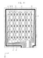
- the touch panel 330 includes a plurality of touch cells arranged in a first direction D 1 and a second direction D 2 .
- FIG. 3 illustrates four touch cells arranged in the first direction D 1 and five touch cells arranged in the second direction D 2
- exemplary embodiments are not limited to a specific number of the touch cells or an arrangement of the touch cells.
- the touch panel 330 include first touch electrodes TA including a plurality of sub electrodes arranged along the first direction D 1 , second touch electrodes TB arranged along the second direction D 2 , and third touch electrodes TC extending along the second direction D 2 .
- the third touch electrodes TC have different shapes than the second touch electrodes TB and the first touch electrodes TA.
- the first touch electrodes TA, the second touch electrodes TB, and the third touch electrodes TC may be disposed on the same plane.
- the first touch electrodes TA, the second touch electrodes TB, and the third touch electrodes TC may be disposed on the encapsulating glass 320 .
- the first touch electrodes TA and the second touch electrodes TB recognize a first touch by a first touch input member.
- the first touch electrodes TA may recognize a touch coordinate of an X-axis of the first touch.
- the second touch electrodes TB may recognize a touch coordinate of a Y-axis of the first touch.
- the first touch input member may be a portion of a human body, such as a human finger, hand, etc.
- the first touch may be defined as a general touch operation.
- the first touch electrodes TA and the third touch electrodes TC recognize a second touch by a second touch input member.
- the second touch input member may be an object other than a portion of the human body.
- the second touch input member may be a touch pen or stylus.
- the second touch may be defined as a digitizer operation.
- First end portions of the first touch electrodes TA may be connected to first lines LA. Second end portions of the first touch electrodes TA may be connected to second lines LB. First end portions of the second touch electrodes TB may be connected to third lines LC. Second end portions of the second touch electrodes TB may not be connected to any lines. First end portions of the third touch electrodes TC may be commonly connected to a fourth line LD. Second end portions of the third touch electrodes TC may be connected to fifth lines LE.
- both the first lines LA and the second lines LB are connected to the first touch driving chip 430 .
- the third lines LC are connected to the first touch driving chip 430 .
- the first touch driving chip 430 may sense the first touch based on signals of the first touch electrodes TA and the second touch electrodes TB transmitted through the first to third lines LA, LB, and LC.
- the first lines LA are connected to the second touch driving chip 440 and the second lines LB are connected to the loop coil 620 .
- the fourth line LD is connected to the loop coil 620 and the fifth lines LE are connected to the second touch driving chip 440 .
- the second touch driving chip 440 may sense the second touch based on signals of the first touch electrodes TA transmitted through the first lines LA, signals of the third touch electrodes TC transmitted through the fifth lines LE, and a signal of the loop coil 620 . A method of recognizing the second touch will be described in more detail with reference to FIG. 7 .
- the first touch electrode TA includes a first sub electrode TA 1 and a second sub electrode TA 2 spaced apart from the first sub electrode TA 1 .
- the second touch electrode TB is disposed between the first sub electrode TA 1 and the second sub electrode TA 2 .
- the touch cell A may further include a first bridge BR 1 and a second BR 2 electrically connecting the first sub electrode TA 1 and the second sub electrode TA 2 and overlapping the second touch electrode TB in a plan view.
- the first and second bridges BR 1 and BR 2 may be plural as shown in FIG. 4 .
- the first and second bridges BR 1 and BR 2 may be configured as a single bridge. When configured as the first and second bridges BR 1 and BR 2 , a resistance of the first touch electrode TA may be reduced.
- the third touch electrode TC may be disposed between first and second sub electrodes TA 1 and TA 2 of different touch cells.
- the third touch electrode TC 1 may be disposed between the first sub electrode TA 1 in the touch cell A and a second sub electrode TA 2 of a neighboring touch cell adjacent to a first side of the touch cell A in the first direction D 1 .
- the third touch electrode TC 2 may be disposed between the second sub electrode TA 2 in the touch cell A and the first sub electrode TA 1 in another neighboring touch cell adjacent to a second side of the touch cell A in the first direction D 1 .
- the touch panel 330 may further include third and fourth bridges BR 3 and BR 4 electrically connecting the second sub electrode TA 2 in the touch cell A and the first sub electrode TA 1 in the another neighboring touch cell and overlapping the third touch electrode TC 2 in a plan view.
- the third and fourth bridges BR 3 and BR 4 may be plural as shown in FIG. 4 .
- the third and fourth bridges may be configured as a single bridge. When configured as the third and fourth bridges BR 3 and BR 4 , a resistance of the first touch electrode TA may be reduced.
- the first sub electrode TA 1 and the second sub electrode TA 2 of the first touch electrode TA, the second touch electrode TB, and the third touch electrode TC may include substantially the same material as one another.
- the first touch electrode TA, the second touch electrode TB, and the third touch electrode TC may include indium tin oxide (ITO), however, it is contemplated that any other suitable material may be utilized in association with exemplary embodiments described herein.
- the first touch electrode TA, the second touch electrode TB, and the third touch electrode TC may be formed of other transparent (or at least translucent) conductive materials, such as aluminum zinc oxide (AZO), gallium zinc oxide (GZO), indium zinc oxide (IZO), etc.
- one or more conductive polymers may be utilized, such as, for example, polyaniline (PANI), poly(3,4-ethylenedioxythiophene) poly(styrenesulfonate) (PEDOT:PSS), etc.
- the first and second bridges BR 1 and BR 2 and the third and fourth bridges BR 3 and BR 4 may include a material different from the material of the first sub electrode TA 1 and the second sub electrode TA 2 of the first touch electrode TA.
- the first to third touch electrodes TA, TB, and TC are included in the touch panel 330 where the first touch electrode TA and the second touch electrode TB operate in conjunction with the first touch operation (the general touch operation) associated with the first touch input member, and the first touch electrode TA and the third touch electrode TC operate in conjunction with the second touch operation (the digitizer operation) associated with the second touch input member.
- the first to third touch electrodes TA, TB, and TC are included in a single touch panel 330 , a width of the display apparatus that is capable of recognizing the first touch and the second touch may be reduced.
- FIG. 5 is a plan view of a touch cell of a touch panel, according to one or more exemplary embodiments. It is noted that the touch panel and the display apparatus associated with the touch cell of FIG. 5 are substantially similar to the touch panel 300 and the display apparatus FIGS. 1 to 4 except for the structure of the touch cell of FIG. 5 . As such, the same reference numerals will be used to refer to the same or like parts as those described in association with FIGS. 1 to 4 , and repetitive explanations have been avoided to prevent obscuring exemplary embodiments described herein.
- a first side of the first sub electrode TA 1 faces a first side of the second touch electrode TB.
- a second side of the first sub electrode TA 1 faces a second side of the second touch electrode TB.
- a first side of the second sub electrode TA 2 faces a third side of the second touch electrode TB.
- a second side of the second sub electrode TA 2 faces a fourth side of the second touch electrode TB.
- the touch cell of FIG. 5 further includes first to fourth dummy electrodes TD 1 to TD 4 .
- the first dummy electrode TD 1 is disposed between the first side of the first sub electrode TA 1 and the first side of the second touch electrode TB
- the second dummy electrode TD 2 is disposed between the second side of the first sub electrode TA 1 and the second side of the second touch electrode TB
- the third dummy electrode TD 3 is disposed between the first side of the second sub electrode TA 2 and the third side of the second touch electrode TB
- the fourth dummy electrode TD 4 is disposed between the second side of the second sub electrode TA 2 and the fourth side of the second touch electrode TB.
- the first to fourth dummy electrodes TD 1 to TD 4 may not be connected any other electrodes or any other lines, and, as such, may be electrically floated.
- the first to fourth dummy electrodes TD 1 to TD 4 may have island shapes; however, it is contemplated that any other suitable configuration may be utilized in association with exemplary embodiments described herein. For instance, as seen in FIG. 5 , the island shapes are island bar shapes.
- the first to fourth dummy electrodes TD 1 to TD 4 may not be disposed in (e.g., spaced apart from) an area where the first and second bridges BR 1 and BR 2 are formed. That is, the first and second bridges BR 1 and BR 2 may not overlap the first to fourth dummy electrodes TD 1 to TD 4 .
- the first touch electrode TA and the second touch electrode TB may function as a transmitter and a receiver, respectively, to recognize the first touch operation.
- a distance between the touch panel 330 and the window 100 may be considered.
- capacitance between the first touch electrode TA and the second touch electrode TB may be relatively strong such that the sensitivity of touch detection may be reduced.
- capacitance between the first touch electrode TA and the second touch electrode TB may not be large enough such that the touch function may not operate normally.
- the first to fourth dummy electrodes TD 1 to TD 4 may be provided between each of the sub electrodes TA 1 and TA 2 of the first touch electrode TA and the second touch electrode TB, and, for example, the gap between each of the sub electrodes TA and TA 2 and the second touch electrode TB may increase. In this manner, the capacitance between the first touch electrode TA and the second touch electrode TB may increase such that a sensitivity of touch detection may also increase.
- FIG. 6A is a cross-sectional view of the touch cell of FIG. 4 taken along sectional line I-I′, according to one or more exemplary embodiments.
- FIG. 6B is a cross-sectional view of the touch cell of FIG. 5 taken along sectional line according to one or more exemplary embodiments.
- a direct magnetic field from the first sub electrode TA 1 to the second touch electrode TB is generated.
- both a direct magnetic field from the first sub electrode TA 1 to the second touch electrode TB and an indirect magnetic field from the first sub electrode TA 1 to the second touch electrode TB via the first dummy electrode TD 1 are generated.
- the magnetic field between the first sub electrode TA 1 and the second touch electrode TB of FIG. 6B may be greater than that of FIG. 6A when the gap between the first sub electrode TA 1 and the second touch electrode TB of FIG. 6B is the same as in FIG. 6A .
- the first to fourth dummy electrodes TD 1 to TD 4 are disposed between the first and second sub electrodes TA 1 and TA 2 and the second touch electrode TB, the sensitivity of touch detection may be improved.
- the first to fourth dummy electrodes TD 1 to TD 4 may be disposed on the same plane as the first and second sub electrodes TA 1 and TA 2 of the first touch electrode TA, the second touch electrode TB, and the third touch electrode TC.
- the first to fourth dummy electrodes TD 1 to TD 4 may include a material substantially the same as the material of the first and second sub electrodes TA 1 and TA 2 of the first touch electrode TA, the second touch electrode TB, and the third touch electrode TC.
- the first to third touch electrodes TA, TB, and TC may be included in a single touch panel where the first touch electrode TA and the second touch electrode TB operate in conjunction with the first touch operation (the general touch operation) associated with the first touch input member, and the first touch electrode TA and the third touch electrode TC operate in conjunction with the second touch operation (the digitizer operation) associated with the second touch input member.
- the first touch electrode TA and the third touch electrode TC operate in conjunction with the second touch operation (the digitizer operation) associated with the second touch input member.
- the first to fourth dummy electrodes TD 1 to TD 4 may be disposed between the first touch electrode TA and the second touch electrode TB so that the sensitivity of touch detection may be improved in association with the first touch operation.
- FIG. 7 is a schematic circuit diagram of a digitizing operation of the touch panel of FIG. 3 , according to one or more exemplary embodiments.
- first end portions of the third touch electrode TC may be connected to the loop coil 620 through the fourth line LD, and the second end portions of the third touch electrode TC may be connected to an amplifier AMP through one of the fifth lines LE.
- the amplifier AMP may output a voltage VO to the second touch driving chip 440 .
- the output voltage VO output through an amplifier AMP when the second touch is generated at a left side A 1 of the third touch electrode TC is different from the output voltage VO output through the amplifier AMP when the second touch is generated at a right side A 2 of the third touch electrode TC.
- the second touch driving chip 440 may determine whether the second touch is generated at A 1 or A 2 .
- the touch coordinates of the X-axis and the Y-axis of the second touch may be determined using the first touch electrodes TA, which are disposed in the first direction D 1 and have first end portions connected to the loop coil 620 and the third touch electrodes TC, which are disposed in the second direction D 2 and have first end portions connected to the loop coil 620 .
- FIG. 8 is a plan view of a touch panel, according to one or more exemplary embodiments.
- FIG. 9 is a plan view of a touch cell of the touch panel of FIG. 8 , according to one or more exemplary embodiments.
- the touch panel and the display apparatus of FIGS. 8 and 9 are substantially the same as the touch panel and the display apparatus of FIGS. 1 to 4 except for the structure of the touch cells. As such, the same reference numerals will be used to refer to the same or like parts as those described in association with FIGS. 1 to 4 , and repetitive explanations have been avoided to prevent obscuring exemplary embodiments described herein.
- the touch cell includes a first touch electrode TA, a second touch electrode TB, and a third touch electrode TC.
- the first touch electrode TA includes a first sub electrode TA 1 and a second sub electrode TA 2 spaced apart from the first sub electrode TA 1 like as described in association with FIG. 4 .
- the second touch electrode TB is disposed between the first sub electrode TA 1 and the second sub electrode TA 2 .
- Each of the third touch electrodes TC 1 and TC 2 is disposed between the sub electrodes TA 1 and TA 2 included in neighboring touch cells.
- the touch cell may further include a first bridge BR 1 electrically connecting the first sub electrode TA 1 and the second sub electrode TA 2 and overlapping the second touch electrode TB in a plan view.
- the first sub electrode TA 1 may include a first inclined portion facing a first side of the second touch electrode TB and a second inclined portion facing a second side of the second touch electrode TB.
- the first inclined portion may have a first bended portion BP 1 .
- the second inclined portion may have a second bended portion BP 2 .
- the second sub electrode TA 2 may be configured similarly to the first sub electrode TA 1 , but in a mirrored fashion with respect to the second touch electrode TB.
- a size of the first touch electrode TA may be adjusted to be substantially the same as a size of the second touch electrode TB in the touch cell.
- the bended portions BP 1 and BP 2 may be formed in the first sub electrode TA 1 and the second sub electrode TA 2 .
- the first to third touch electrodes TA, TB, and TC are integrated in a single touch panel where the first touch electrode TA and the second touch electrode TB operate in conjunction with the first touch operation (the general touch operation) in association with the first touch input member, and the first touch electrode TA and the third touch electrode TC operate in conjunction with the second touch operation (the digitizer operation) in association with the second touch input member.
- the first touch electrode TA and the third touch electrode TC operate in conjunction with the second touch operation (the digitizer operation) in association with the second touch input member.
- a width of the display apparatus configured to detect the first touch and the second touch may be reduced.
- a size of the first touch electrode TA and a size of the second touch electrode TB are substantially the same as each other in the touch cell so that reliability of the first touch operation may be improved.
- FIG. 10 is a plan view of a touch cell of a touch panel, according to one or more exemplary embodiments.
- the touch panel and the display apparatus of FIG. 10 are substantially the same as the touch panel and the display apparatus of FIGS. 8 and 9 except for the structure of the touch cells. As such, the same reference numerals will be used to refer to the same or like parts as those described in association with FIGS. 8 and 9 , and repetitive explanations have been avoided to prevent obscuring exemplary embodiments described herein.
- the touch cell further includes first to fourth dummy electrodes TD 1 to TD 4 .
- the first dummy electrode TD 1 is disposed between a first inclined portion of the first sub electrode TA 1 and a first inclined portion of the second touch electrode TB
- the second dummy electrode TD 2 is disposed between a first inclined portion of the second sub electrode TA 2 and a third inclined portion of the second touch electrode TB
- the third dummy electrode TD 3 is disposed between a second inclined portion of the first sub electrode TA 1 and a second inclined portion of the second touch electrode TB
- the fourth dummy electrode TD 4 is disposed between a second inclined portion of the second sub electrode TA 2 and a fourth inclined portion of the second touch electrode TB.
- the first to fourth dummy electrodes TD 1 to TD 4 may not be connected any electrodes or any lines, and, as such, may be electrically floated.
- the first to fourth dummy electrodes TD 1 to TD 4 may have island shapes; however, it is contemplated that any other suitable configuration may be utilized in association with exemplary embodiments described herein.
- the first to fourth dummy electrodes TD 1 to TD 4 may have a bended portion corresponding to a bended portion of an adjacent sub electrode.
- the first dummy electrode TD 1 may have a bended portion corresponding to the first bended portion BP 1 and the second dummy electrode TD 2 may have a bended portion corresponding to the second bended portion BP 2 .
- the first to fourth dummy electrodes TD 1 to TD 4 may not be disposed in an area where the first bridge BR 1 is disposed.
- the third touch electrodes TC may have variable widths in the first direction D 1 , which may vary as a function in the second direction D 2 .
- the third touch electrode TC 1 may have a relatively greater width in the first direction D 1 at upper and lower portions of the touch cell and a relatively shorter width in the first direction D 1 at a central portion of the touch cell, such as where a second bridge BR 2 is disposed. In this manner, the width of the third touch electrode TC 1 may vary from the relatively greater width to the relatively smaller width back to the relatively greater width along a length of the third touch electrode TC 1 .
- the first to third touch electrodes TA, TB, and TC are included in a single touch panel where the first touch electrode TA and the second touch electrode TB operate in conjunction with the first touch operation (the general touch operation) associated with the first touch input member, and the first touch electrode TA and the third touch electrode TC operate in conjunction with the second touch operation (the digitizer operation) associated with the second touch input member.
- the width of the display apparatus configured to recognize the first touch and the second touch may be reduced.
- the first to fourth dummy electrodes TD 1 to TD 4 are disposed between the first and second sub electrodes TA 1 and TA 2 and the second touch electrode TB, the sensitivity of touch detection may be improved for the first touch operation.
- FIG. 11 is a plan view of a touch panel, according to one or more exemplary embodiments.
- FIG. 12 is a plan view of a touch cell of the touch panel of FIG. 11 , according to one or more exemplary embodiments.
- the touch panel and the display apparatus of FIGS. 11 and 12 are substantially the same as the touch panel and the display apparatus of FIGS. 1 to 4 except for the structure of the touch cells.
- the same reference numerals will be used to refer to the same or like parts as those described in association with FIGS. 1 to 4 , and repetitive explanations have been avoided to prevent obscuring exemplary embodiments described herein.
- the touch cell includes a first touch electrode TA, a second touch electrode TB, and a third touch electrode TC.
- the first touch electrode TA includes a first sub electrode TA 1 and a second sub electrode TA 2 spaced apart from the first sub electrode TA 1 .
- the second touch electrode TB is disposed between the first sub electrode TA 1 and the second sub electrode TA 2 .
- Each of the third touch electrodes TC 1 and TC 2 is disposed between the sub electrodes TA 1 and TA 2 of neighboring touch cells.
- the first touch electrode TA may further include first and second connecting electrodes TAS 1 and TAS 2 . It is noted that the first and second connecting electrodes TAS 1 and TAS 2 may overlap the second touch electrode TB, as seen in FIG. 12 .
- the touch cell further includes first to fourth bridges BR 1 to BR 4 .
- the first bridge BR 1 electrically connects the first sub electrode TA 1 and a first connecting electrode TAS 1 , and the first bridge BR 1 overlaps the second touch electrode TB in a plan view.
- the second bridge BR 2 electrically connects the second sub electrode TA 2 and the first connecting electrode TAS 1 , and the second bridge BR 2 overlaps the second touch electrode TB in a plan view.
- the third bridge BR 3 electrically connects the first sub electrode TA 1 and a second connecting electrode TAS 2 , and the third bridge BR 3 overlaps the second touch electrode TB in a plan view.
- the fourth bridge BR 4 electrically connects the second sub electrode TA 2 and the second connecting electrode TAS 2 , and the fourth bridge BR 4 overlaps the second touch electrode TB in a plan view.
- the first sub electrode TA 1 and the second sub electrode TA 2 are connected to each other by the first to fourth bridges BR 1 to BR 4 and the first and second connecting electrodes TAS 1 and TAS 2 so that the resistance may be reduced as compared to when the first sub electrode TA 1 and the second sub electrode TA 2 are connected to each other with only the bridges, e.g., first and second bridges BR 1 and BR 2 of FIG. 4 .
- the presence of the first and second connecting electrodes TAS 1 and TAS 2 enables the respective lengths of the first to fourth bridges BR 1 to BR 4 to be relatively shorter. As such, the first to fourth bridges BR 1 to BR 4 may not visible to a user.
- the touch cell may further include additional connecting electrodes and fifth to eighth bridges BR 5 to BR 8 .
- the additional connecting electrodes may be surrounded by (or otherwise overlap) the third touch electrode TC, e.g., third touch electrodes TC 1 and TC 2 .
- the first sub electrode TA 1 may be connected to the second sub electrode TA 2 of an adjacent touch cell through the fifth and sixth bridges BR 5 and BR 6 and corresponding connecting electrodes.
- the second sub electrode TA 2 may be connected to the first sub electrode TA 1 of another adjacent touch cell through the seventh and eighth bridges BR 7 and BR 8 and corresponding connecting electrodes.
- the first sub electrode TA 1 may include a first inclined portion facing a first side of the second touch electrode TB and a second inclined portion facing a second side of the second touch electrode TB.
- a contact point CP of the first inclined portion and the second inclined portion may have a concave portion.
- the second sub electrode TA 2 may also be configured including a contact point and associated concave portion.
- the second touch electrode TB may have a convex portion corresponding to the concave portion of the first sub electrode TA 1 and the concave portion of the second sub electrode TA 2 . In this manner, electrode resistance of the second touch electrode TB may be reduced. Further, the length of the bridge connecting the first sub electrode TA 1 and the second sub electrode TA 2 may be reduced.
- the first sub electrode TA 1 and second sub electrode TA 2 may also include additional concave portions respectively facing the third touch electrodes TC 1 and TAC 2 .
- the third touch electrodes TC 1 and TAC 2 may include convex portions corresponding to the concave portions of the first sub electrode TA 1 and the second sub electrode TA 2 .
- the first to third touch electrodes TA, TB, and TC are included in a single touch panel where the first touch electrode TA and the second touch electrode TB operate in conjunction with the first touch operation (the general touch operation) associated with the first touch input member and the first touch electrode TA and the third touch electrode TC operate in conjunction with the second touch operation (the digitizer operation) associated with the second touch input member.
- the width of an associated display apparatus configured to recognize the first touch and the second touch may be reduced.
- the resistance of the bridge in the touch cell may be reduced and the bridge may be less visible (or invisible) to a user.
- FIG. 13 is a plan view of a touch cell of a touch panel, according to one or more exemplary embodiments.
- the touch panel and the display apparatus of FIG. 13 are substantially the same as the touch panel and the display apparatus of FIGS. 11 and 12 except for the structure of the touch cells. As such, the same reference numerals will be used to refer to the same or like parts as those described in association with FIGS. 11 and 12 , and repetitive explanations have been avoided to prevent obscuring exemplary embodiments described herein.
- the touch cell further includes first to fourth dummy electrodes TD 1 to TD 4 .
- the first dummy electrode TD 1 is disposed between a first inclined portion of the first sub electrode TA 1 and a first inclined portion of the second touch electrode TB
- the second dummy electrode TD 2 is disposed between a first inclined portion of the second sub electrode TA 2 and a third inclined portion of the second touch electrode TB
- the third dummy electrode TD 3 is disposed between a second inclined portion of the first sub electrode TA 1 and a second inclined portion of the second touch electrode TB
- the fourth dummy electrode TD 4 is disposed between a second inclined portion of the second sub electrode TA 2 and a fourth inclined portion of the second touch electrode TB.
- the first to fourth dummy electrodes TD 1 to TD 4 may not be connected any electrodes or any lines, and, as such, may be electrically floated.
- the first to fourth dummy electrodes TD 1 to TD 4 may have island shapes; however, it is contemplated that any other suitable configuration may be utilized in association with exemplary embodiments described herein.
- the first to fourth dummy electrodes TD 1 to TD 4 may not be disposed in an area where the first to fourth bridges BR 1 to BR 4 are formed.
- a third touch electrodes TC may have variable width in the first direction D 1 , which may vary as a function in the second direction D 2 .
- the third touch electrode TC 1 may have a relatively greater width in the first direction D 1 at upper and lower portions of the touch cell and a relatively shorter width in the first direction D 1 at a central portion of the touch cell, such as where the fifth and sixth second bridges BR 5 and BR 6 are disposed.
- the width of the third touch electrode TC 1 may vary from the relatively greater width to the relatively smaller width back to the relatively greater width along a length of the third touch electrode TC 1 .
- the first to third touch electrodes TA, TB, and TC are included in a single touch panel where the first touch electrode TA and the second touch electrode TB operate in conjunction with the first touch operation (the general touch operation) associated with the first touch input member, and the first touch electrode TA and the third touch electrode TC operate in conjunction with the second touch operation (the digitizer operation) associated with the second touch input member.
- the width of the display apparatus configured to recognize the first touch and the second touch may be reduced.
- the first to fourth dummy electrodes TD 1 to TD 4 are disposed between the first and second sub electrodes TA 1 and TA 2 and the second touch electrode TB, the sensitivity of touch detection may be improved for the first touch operation.
- the resistance of the bridges e.g., the first to eighth bridges BR 1 to BR 8 , in the touch cell may be reduced and the bridges may be less visible (or invisible) to a user.
- FIG. 14 is a plan view of a touch panel, according to one or more exemplary embodiments.
- FIG. 15 is a plan view of a touch cell of the touch panel of FIG. 14 , according to one or more exemplary embodiments.
- the touch panel and the display apparatus of FIGS. 14 and 15 are substantially the same as the touch panel and the display apparatus of FIGS. 11 to 12 except for the structure of the touch cell. As such, the same reference numerals will be used to refer to the same or like parts as those described in association with FIGS. 11 to 12 , and repetitive explanations have been avoided to prevent obscuring exemplary embodiments described herein.
- the touch cell includes a first touch electrode TA, a second touch electrode TB, and a third touch electrode TC.
- the first touch electrode TA includes a first sub electrode TA 1 and a second sub electrode TA 2 spaced apart from the first sub electrode TA 1 .
- the second touch electrode TB is disposed between the first sub electrode TA 1 and the second sub electrode TA 2 .
- Each of the third touch electrodes TC 1 and TC 2 is disposed between the sub electrodes TA 1 and TA 2 of neighboring touch cells.
- the first touch electrode TA may further include first and second connecting electrodes TAS 1 and TAS 2 . It is noted that the first and second connecting electrodes TAS 1 and TAS 2 may overlap the second touch electrode TB, as seen in FIG. 15 .
- the touch cell further includes first to fourth bridges BR 1 to BR 4 .
- the first bridge BR 1 electrically connects the first sub electrode TA 1 and a first connecting electrode TAS 1 , and the first bridge BR 1 overlaps the second touch electrode TB in a plan view.
- the second bridge BR 2 electrically connects the second sub electrode TA 2 and the first connecting electrode TAS 1 , and the second bridge BR 2 overlaps the second touch electrode TB in a plan view.
- the third bridge BR 3 electrically connects the first sub electrode TA 1 and a second connecting electrode TAS 2 , and the third bridge BR 3 overlaps the second touch electrode TB in a plan view.
- the fourth bridge BR 4 electrically connects the second sub electrode TA 2 and the second connecting electrode TAS 2 , and the fourth bridge BR 4 overlaps the second touch electrode TB in a plan view.
- the first sub electrode TA 1 may include a first inclined portion facing a first inclined portion of the second touch electrode TB and a second inclined portion facing a second inclined portion of the second touch electrode TB.
- the first inclined portion and the second inclined portion of the first sub electrode TA 1 may have zigzag shapes.
- the first inclined portion and the second inclined portion of the second touch electrode TB may also have zigzag shapes.
- sides of the first sub electrode TA 1 and sides of the third touch electrode TC 1 facing each other may have corresponding zigzag shapes.
- the configuration of the second sub electrode TA 2 , the second touch electrode TB, and the third touch electrode TC 2 may be similar to the configuration of the first sub electrode TA 1 , the second touch electrode TB, and the third touch electrode TC 1 .
- Display cells of a display panel may generally be arranged in a matrix formation.
- the touch cells are arranged in a matrix formation or mainly have a rectilinear structure like the display cells, moiré fringe patterns may be visible to the user.
- the sides of the first touch electrode TA, the second touch electrode TB, and the third touch electrode TC have zigzag shapes, a display defect due to the moiré fringe patterns may be prevented (or at least reduced).
- the first to third touch electrodes TA, TB, and TC are included in a single touch panel where the first touch electrode TA and the second touch electrode TB operate in conjunction with the first touch operation (the general touch operation) associated with the first touch input member and the first touch electrode TA and the third touch electrode TC operate in conjunction with the second touch operation (the digitizer operation) associated with the second touch input member.
- the width of an associated display apparatus configured to recognize the first touch and the second touch may be reduced.
- the resistance of the bridge in the touch cell may be reduced and the bridge may be less visible (or invisible) to a user.
- the sides of the first to third touch electrodes TA, TB, and TC have zigzag shapes so that a display defect due to the moiré fringe patterns may be prevented (or at least reduced).
- FIG. 16 is a plan view of a touch cell of a touch panel, according to one or more exemplary embodiments.
- the touch panel and the display apparatus of FIG. 16 are substantially the same as the touch panel and the display apparatus of FIGS. 14 and 15 except for the structure of the touch cells. As such, the same reference numerals will be used to refer to the same or like parts as those described in association with FIGS. 14 and 15 , and repetitive explanations have been avoided to prevent obscuring exemplary embodiments described herein.
- the touch cell further includes first to fourth dummy electrodes TD 1 to TD 4 .
- the first dummy electrode TD 1 is disposed between a first inclined portion of the first sub electrode TA 1 and a first inclined portion of the second touch electrode TB
- the second dummy electrode TD 2 is disposed between a first inclined portion of the second sub electrode TA 2 and a third inclined portion of the second touch electrode TB
- the third dummy electrode TD 3 is disposed between a second inclined portion of the first sub electrode TA 1 and a second inclined portion of the second touch electrode TB
- the fourth dummy electrode TD 4 is disposed between a second inclined portion of the second sub electrode TA 2 and a fourth inclined portion of the second touch electrode TB.
- the first to fourth dummy electrodes TD 1 to TD 4 may not be connected any electrodes or any lines, and, as such, may be electrically floated.
- the first to fourth dummy electrodes TD 1 to TD 4 may have island shapes; however, it is contemplated that any other suitable configuration may be utilized in association with exemplary embodiments described herein.
- the first to fourth dummy electrodes TD 1 to TD 4 may not be disposed in an area where the first to fourth bridges BR 1 to BR 4 are formed.
- the first to fourth dummy electrodes TD 1 to TD 4 may also have zigzag shapes corresponding to the zigzag shapes of the first and second sub electrodes TA 1 and TA 2 and the second touch electrode TB.
- the first to third touch electrodes TA, TB, and TC are included in a single touch panel where the first touch electrode TA and the second touch electrode TB operate in conjunction with the first touch operation (the general touch operation) associated with the first touch input member, and the first touch electrode TA and the third touch electrode TC operate in conjunction with the second touch operation (the digitizer operation) associated with the second touch input member.
- the width of the display apparatus configured to recognize the first touch and the second touch may be reduced.
- the first to fourth dummy electrodes TD 1 to TD 4 are disposed between the first and second sub electrodes TA 1 and TA 2 and the second touch electrode TB, the sensitivity of touch detection may be improved for the first touch operation.
- the resistance of the bridges, e.g., the first to eighth bridges BR 1 to BR 8 , in the touch cell may be reduced and the bridges may be less visible (or invisible) to a user.
- the sides of the first to third touch electrodes TA, TB and TC have zigzag shapes so that a display defect due to moiré fringe patterns may be prevented (or at least reduced).
- FIG. 17 is a plan view of a touch panel, according to one or more exemplary embodiments.
- FIG. 18 is a plan view of a touch cell of the touch panel of FIG. 17 , according to one or more exemplary embodiments.
- the touch panel and the display apparatus of FIGS. 17 and 18 are substantially the same as the touch panel and the display apparatus of FIGS. 1 to 4 except for the structure of the touch cells. As such, the same reference numerals will be used to refer to the same or like parts as those described in association with FIGS. 1 to 4 , and repetitive explanations have been avoided to prevent obscuring exemplary embodiments described herein.
- the touch cell includes a first touch electrode TA, a second touch electrode TB, and a third touch electrode TC.
- the first touch electrode TA includes a first sub electrode TA 1 and a second sub electrode TA 2 spaced apart from the first sub electrode TA 1 .
- the second touch electrode TB includes third and fourth sub electrodes TB 1 and TB 2 disposed between the first sub electrode TA 1 and the second sub electrode TA 2 .
- the third and fourth sub electrodes TB 1 and TB 2 are spaced apart from one another with the third touch electrode TC disposed therebetween.
- the first sub electrode TA 1 and the second sub electrode TA 2 are electrically connected to each other via a first bridge BR 1 .
- the first bridge BR 1 may overlap a portion of the second touch electrode TB and the third touch electrode TC.
- the third and fourth sub electrodes TB 1 and TB 2 are electrically connected to each other via a second bridge BR 2 .
- the second bridge BR 2 may overlap a portion of the third touch electrode TC.
- the third touch electrode TC may have a variable width in the first direction D 1 as a function in the second direction D 2 .
- the third touch electrode TC may have a relatively greater width in the first direction D 1 at upper and lower portions of the touch cell but a relatively shorter width in the first direction D 1 at a central portion of the touch cell. In this manner, the width of the third touch electrode TC may vary from the relatively greater width to the relatively smaller width back to the relatively greater width along a length of the third touch electrode TC.
- the first to third touch electrodes TA, TB, and TC are included in a single touch panel where the first touch electrode TA and the second touch electrode TB operate in conjunction with the first touch operation (the general touch operation) associated with the first touch input member, and the first touch electrode TA and the third touch electrode TC operate in conjunction with the second touch operation (the digitizer operation) associated with the second touch input member. Accordingly, the width of the display apparatus that is configured to recognize the first touch and the second touch may be reduced.
- FIG. 19 is a plan view of a touch cell of a touch panel, according to one or more exemplary embodiments. It is noted that the touch panel and the display apparatus associated with the touch cell of FIG. 19 are substantially similar to the touch panel and the display apparatus FIGS. 17 and 18 except for the structure of the touch cell of FIG. 19 . As such, the same reference numerals will be used to refer to the same or like parts as those described in association with FIGS. 17 and 18 , and repetitive explanations have been avoided to prevent obscuring exemplary embodiments described herein.
- the touch cell further includes first to fourth dummy electrodes TD 1 to TD 4 .
- the first dummy electrode TD 1 and the third dummy electrode TD 3 are disposed between the first sub electrode TA 1 and the third sub electrode TB 1 .
- the second dummy electrode TD 2 and the fourth dummy electrode TD 4 are disposed between the second sub electrode TA 2 and the fourth sub electrode TB 2 .
- the first to third touch electrodes TA, TB, and TC are integrated in a single touch panel where the first touch electrode TA and the second touch electrode TB operate in conjunction with the first touch operation (the general touch operation) in association with the first touch input member, and the first touch electrode TA and the third touch electrode TC operate in conjunction with the second touch operation (the digitizer operation) in association with the second touch input member.
- the first touch electrode TA and the third touch electrode TC operate in conjunction with the second touch operation (the digitizer operation) in association with the second touch input member.
- the first to fourth dummy electrodes TD 1 to TD 4 are disposed between the first touch electrode TA and the second touch electrode TB so that the sensitivity of touch detection may be improved for the first touch operation.
- FIG. 20 is an exploded perspective view of a display apparatus, according to one or more exemplary embodiments.
- the display apparatus of FIG. 20 is substantially similar to the display apparatus of FIGS. 1 and 2 except for certain components, such as the cushion sheet and heat dissipating member.
- certain components such as the cushion sheet and heat dissipating member.
- the same reference numerals will be used to refer to the same or like parts as those described in association with FIGS. 1 and 2 , and repetitive explanations have been avoided to prevent obscuring exemplary embodiments described herein.
- the display apparatus includes a window 100 , a polarizing plate 200 , a touch display panel 300 , a driver 400 , and a power coil member 500 A.
- the window 100 , the polarizing plate 200 , the touch display panel 300 , and the driver 400 may be configured and operate similar to the window 100 , the polarizing plate 200 , the touch display panel 300 , and the driver 400 described in association with FIG. 1 .
- the power coil member 500 A includes a cushion sheet, a power coil, a magnetic shielding material, and a heat dissipating member.
- the cushion sheet, the power coil, the magnetic shielding material, and the heat dissipating member are integrated to form the power coil member 500 A.
- the power coil member 500 A is disposed under the touch display panel 300 , and will be described in more detail in association with FIGS. 21A to 21D .
- FIGS. 21A, 21B, 21C, and 21D are perspective views of a method of manufacturing an integrated component of a touch panel, according to one or more exemplary embodiments.
- the power coil member 500 A includes a cushion sheet 510 protecting the touch display panel 300 from an external force.
- the power coil 520 may be formed on the cushion sheet 510 , and may provide energy to a second touch input member, such as a touch pen having a LC circuit.
- a loop coil 530 may be formed adjacent to the power coil 520 .
- the power coil member 500 A further includes a heat dissipating member 540 and a magnetic shielding material 550 .
- the heat dissipating member 540 may be formed under (or attached to) the cushion sheet 510 and may dissipate heat from the display panel.
- the heat dissipating member 540 may include graphite.
- the magnetic shielding material 550 may be formed on the heat dissipating member 540 .
- the magnetic shielding material 550 may be coated on the heat dissipating member 540 .
- the cushion sheet 510 including the power coil 520 and the loop coil 530 may be integrated as a component of the display apparatus of FIG. 20 .
- the first to third touch electrodes TA, TB, and TC are integrated in a single touch panel where the first touch electrode TA and the second touch electrode TB operate in conjunction with the first touch operation (the general touch operation) associated with the first touch input member, and the first touch electrode TA and the third touch electrode TC operate in conjunction with the second touch operation (the digitizer operation) associated with the second touch input member.
- the width of the display apparatus of FIG. 20 that is capable of recognizing the first touch and the second touch may be reduced.
- the thickness of the display apparatus of FIG. 20 may be reduced and manufacturing costs of the display apparatus may also be reduced.
- FIG. 22 is a plan view of a touch panel, according to one or more exemplary embodiments.
- the display apparatus of FIG. 22 is substantially similar to the display apparatus of FIGS. 1 and 2 except for the configuration of the touch display panel. As such, the same reference numerals will be used to refer to the same or like parts as those described in association with FIGS. 1 and 2 , and repetitive explanations have been avoided to prevent obscuring exemplary embodiments described herein.
- the touch panel includes first touch electrodes TA, second touch electrodes TB, third touch electrodes TC, first lines LA, second lines LB, third lines LC, a fourth line LD, fifth lines LE, a guard ring GR, and a loop coil LOC.
- the first touch electrodes TA, the second touch electrodes TB, the third touch electrodes TC, the first lines LA, the second lines LB, the third lines LC, the fourth line LD, and the fifth lines LE may be configured and operate similar to the first touch electrodes TA, the second touch electrodes TB, the third touch electrodes TC, the first lines LA, the second lines LB, the third lines LC, the fourth line LD, and the fifth lines LE described in association with FIG. 3 .
- the guard ring GR may surround and protect the first touch electrodes TA, the second touch electrodes TB, the third touch electrodes TC, and the lines LA, LB, LC, LD, and LE from static electricity.
- the guard ring GR includes a plurality of conductive lines.
- the guard ring GR may form a power coil so that a current flowing through the conductive lines of the guard ring GR may provide energy to the touch input member, e.g., a stylus.
- the loop coil LOC may be disposed adjacent to the guard ring GR, such that the loop coil LOC is disposed between the guard ring GR and the edge of the touch panel. In this manner, the power coil 610 and the loop coil 620 shown in FIG. 1 may be omitted.
- the first to third touch electrodes TA, TB, and TC are included in a single touch panel where the first touch electrode TA and the second touch electrode TB operate in conjunction with the first touch operation (the general touch operation) associated with the first touch input member, and the first touch electrode TA and the third touch electrode TC operate in conjunction with the second touch operation (the digitizer operation) associated with the second touch input member.
- the width of the display apparatus configured to recognize the first touch and the second touch may be reduced.
- the power coil may be formed on the touch panel so that a conventional power coil sheet may be omitted. As such, a thickness of the display apparatus may be reduced and manufacturing costs of the display apparatus may also be reduced.
- FIG. 23A is a perspective view of a window of a display apparatus, according to one or more exemplary embodiments.
- FIG. 23B is a plan view of a rear surface of the window of FIG. 23A , according to one or more exemplary embodiments.
- the window 100 may include a power coil 110 and a loop coil 120 .
- the power coil 110 may be disposed in a light blocking area BM on a rear surface of the window 100 .
- the power coil 110 may provide energy to a second touch input member, such as a touch pen having a LC circuit.
- the loop coil 120 may also be disposed in the light blocking area BM on the rear surface of the window 100 .
- the loop coil 120 may be disposed adjacent to the power coil 110 .
- the loop coil 120 may be connected to an electrode of the touch panel to recognize the touch of the second touch input member. In this manner, the power coil 610 and the loop coil 620 shown in FIG. 1 may be omitted.
- the first to third touch electrodes TA, TB, and TC are integrated in a single touch panel where the first touch electrode TA and the second touch electrode TB operate in conjunction with the first touch operation (the general touch operation) associated with the first touch input member, and the first touch electrode TA and the third touch electrode TC operate in conjunction with the second touch operation (the digitizer operation) associated with the second touch input member.
- the width of an associated display apparatus that is capable of recognizing the first touch and the second touch may be reduced.
- the power coil may be formed on the rear surface of the window 100 so that a conventional power coil sheet may be omitted. As such, a thickness of the display apparatus may be reduced and manufacturing costs of the display apparatus may also be reduced.
- first to third touch electrodes for sensing a first touch operation and a second touch operation may be integrated in a single touch panel. In this manner, a thickness of the display apparatus may be reduced.
Priority Applications (2)
| Application Number | Priority Date | Filing Date | Title |
|---|---|---|---|
| US16/688,279 US11023083B2 (en) | 2015-11-13 | 2019-11-19 | Touch panel and display apparatus including the same |
| US17/334,784 US11669212B2 (en) | 2015-11-13 | 2021-05-30 | Touch panel and display apparatus including the same |
Applications Claiming Priority (2)
| Application Number | Priority Date | Filing Date | Title |
|---|---|---|---|
| KR1020150160020A KR102410661B1 (ko) | 2015-11-13 | 2015-11-13 | 터치 패널 및 이를 포함하는 표시 장치 |
| KR10-2015-0160020 | 2015-11-13 |
Related Child Applications (1)
| Application Number | Title | Priority Date | Filing Date |
|---|---|---|---|
| US16/688,279 Continuation US11023083B2 (en) | 2015-11-13 | 2019-11-19 | Touch panel and display apparatus including the same |
Publications (2)
| Publication Number | Publication Date |
|---|---|
| US20170139525A1 US20170139525A1 (en) | 2017-05-18 |
| US10514800B2 true US10514800B2 (en) | 2019-12-24 |
Family
ID=57240995
Family Applications (3)
| Application Number | Title | Priority Date | Filing Date |
|---|---|---|---|
| US15/279,378 Active 2036-12-29 US10514800B2 (en) | 2015-11-13 | 2016-09-28 | Touch panel and display apparatus including the same |
| US16/688,279 Active US11023083B2 (en) | 2015-11-13 | 2019-11-19 | Touch panel and display apparatus including the same |
| US17/334,784 Active US11669212B2 (en) | 2015-11-13 | 2021-05-30 | Touch panel and display apparatus including the same |
Family Applications After (2)
| Application Number | Title | Priority Date | Filing Date |
|---|---|---|---|
| US16/688,279 Active US11023083B2 (en) | 2015-11-13 | 2019-11-19 | Touch panel and display apparatus including the same |
| US17/334,784 Active US11669212B2 (en) | 2015-11-13 | 2021-05-30 | Touch panel and display apparatus including the same |
Country Status (4)
| Country | Link |
|---|---|
| US (3) | US10514800B2 (ko) |
| EP (1) | EP3168722B1 (ko) |
| KR (2) | KR102410661B1 (ko) |
| CN (2) | CN113325972A (ko) |
Cited By (6)
| Publication number | Priority date | Publication date | Assignee | Title |
|---|---|---|---|---|
| US20220294959A1 (en) * | 2019-08-13 | 2022-09-15 | Lg Innotek Co., Ltd. | Image stabilizing coil member and camera module comprising same |
| US11455006B2 (en) * | 2020-09-21 | 2022-09-27 | Samsung Display Co., Ltd. | Display device |
| US11508790B2 (en) | 2018-09-10 | 2022-11-22 | Samsung Display Co., Ltd. | Display device |
| US11614842B2 (en) | 2020-10-05 | 2023-03-28 | Samsung Display Co., Ltd. | Electronic device comprising a display panel and an input sensor on the display panel |
| US20230128593A1 (en) * | 2021-10-21 | 2023-04-27 | Wuhan China Star Optoelectronics Semiconductor Display Technology Co., Ltd. | Touch panel and mobile terminal |
| US20230259240A1 (en) * | 2022-02-17 | 2023-08-17 | Samsung Display Co., Ltd. | Electronic device |
Families Citing this family (29)
| Publication number | Priority date | Publication date | Assignee | Title |
|---|---|---|---|---|
| KR102259430B1 (ko) * | 2014-06-19 | 2021-06-02 | 엘지이노텍 주식회사 | 파워 코일 패턴이 형성된 터치 팬을 이용한 터치 패널 |
| CN106160047B (zh) * | 2015-04-13 | 2019-05-31 | 联想(北京)有限公司 | 一种无线充电装置、电子设备和信息处理方法 |
| CN105468204B (zh) * | 2016-02-04 | 2018-07-17 | 京东方科技集团股份有限公司 | 一种显示模组、显示装置 |
| US10915193B2 (en) * | 2016-08-25 | 2021-02-09 | Hefei Xinsheng Optoelectronics Technology Co., Ltd. | Touch panel, display device and manufacturing method of touch panel |
| CN106843616B (zh) * | 2017-01-03 | 2020-05-19 | 京东方科技集团股份有限公司 | 一种触控基板及其制作方法、触控显示装置 |
| KR102425832B1 (ko) | 2017-06-05 | 2022-07-29 | 삼성디스플레이 주식회사 | 전자 장치 |
| CN109388294B (zh) * | 2017-08-11 | 2021-01-22 | 京东方科技集团股份有限公司 | 触控面板及其制作方法、触控显示装置 |
| CN109426373A (zh) * | 2017-08-21 | 2019-03-05 | 京东方科技集团股份有限公司 | 触控面板及其制作方法、触控显示装置 |
| CN209606950U (zh) * | 2017-08-22 | 2019-11-08 | 东友精细化工有限公司 | 触摸传感器和包括该触摸传感器的图像显示设备 |
| CN109426389B (zh) * | 2017-09-05 | 2021-03-02 | 京东方科技集团股份有限公司 | 触控基板及其制备方法、显示面板 |
| CN107632740B (zh) * | 2017-10-23 | 2023-10-31 | 京东方科技集团股份有限公司 | 触控基板及其制备方法和触控装置 |
| KR102412232B1 (ko) * | 2017-11-17 | 2022-06-23 | 엘지디스플레이 주식회사 | 터치센서를 포함하는 표시장치 및 그의 제조방법 |
| CN207780740U (zh) * | 2017-11-30 | 2018-08-28 | 云谷(固安)科技有限公司 | 一种触控面板和触控显示装置 |
| US10908753B2 (en) * | 2018-04-13 | 2021-02-02 | Tactual Labs Co. | Capacitively coupled conductors |
| KR102475958B1 (ko) | 2018-04-27 | 2022-12-09 | 삼성디스플레이 주식회사 | 터치 센서 |
| KR102639450B1 (ko) | 2018-07-02 | 2024-02-23 | 삼성디스플레이 주식회사 | 감지 유닛 |
| KR102607494B1 (ko) * | 2018-07-06 | 2023-12-01 | 삼성디스플레이 주식회사 | 입력 감지 유닛 및 이를 포함하는 표시장치 |
| KR102551226B1 (ko) * | 2018-07-25 | 2023-07-04 | 삼성디스플레이 주식회사 | 터치 부재 및 터치 부재를 구비하는 표시장치 |
| KR101952770B1 (ko) * | 2018-08-02 | 2019-02-27 | 동우 화인켐 주식회사 | 터치 센서 |
| CN109669573B (zh) * | 2018-12-17 | 2022-04-12 | 武汉天马微电子有限公司 | 触控显示面板及触控显示装置 |
| KR20200126471A (ko) * | 2019-04-29 | 2020-11-09 | 삼성디스플레이 주식회사 | 입력감지회로 및 이를 포함하는 표시모듈 |
| KR20200135634A (ko) * | 2019-05-23 | 2020-12-03 | 삼성디스플레이 주식회사 | 터치 센서 및 이를 구비한 표시 장치 |
| US11871113B2 (en) * | 2019-10-16 | 2024-01-09 | Lg Innotek Co., Ltd. | Coil member for correcting hand-shake and camera module having the same |
| KR20210081665A (ko) * | 2019-12-24 | 2021-07-02 | 동우 화인켐 주식회사 | 터치 센서 및 이를 포함하는 화상 표시 장치 |
| KR20220001036A (ko) * | 2020-06-26 | 2022-01-05 | 삼성디스플레이 주식회사 | 전자 장치 |
| US11327620B1 (en) * | 2020-11-06 | 2022-05-10 | Tpk Advanced Solutions Inc. | Touch sensing layer and touch panel |
| KR20220086310A (ko) * | 2020-12-16 | 2022-06-23 | 엘지디스플레이 주식회사 | 터치표시장치 및 이의 구동방법 |
| KR20220129123A (ko) * | 2021-03-15 | 2022-09-23 | 삼성디스플레이 주식회사 | 표시 장치 |
| KR20220169972A (ko) * | 2021-06-21 | 2022-12-29 | 삼성디스플레이 주식회사 | 터치 부재 및 이를 포함하는 표시 장치 |
Citations (15)
| Publication number | Priority date | Publication date | Assignee | Title |
|---|---|---|---|---|
| US20090315854A1 (en) * | 2008-06-18 | 2009-12-24 | Epson Imaging Devices Corporation | Capacitance type input device and display device with input function |
| US20110007020A1 (en) | 2009-04-10 | 2011-01-13 | Seung Jae Hong | Touch sensor panel design |
| US20110242050A1 (en) * | 2010-04-06 | 2011-10-06 | Samsung Electronics Co., Ltd. | Method and apparatus compensating parasitic capacitance in touch panel |
| US20130257786A1 (en) * | 2012-03-30 | 2013-10-03 | Sharp Kabushiki Kaisha | Projected capacitance touch panel with reference and guard electrode |
| US20140071083A1 (en) * | 2012-09-10 | 2014-03-13 | Samsung Electro-Mechanics Co., Ltd. | Digitizer |
| US20140152919A1 (en) * | 2006-05-05 | 2014-06-05 | Harald Philipp | Touch Screen Element |
| US20140192009A1 (en) | 2013-01-07 | 2014-07-10 | Novatek Microelectronics Corp. | Touch panel |
| US20140198078A1 (en) * | 2007-12-24 | 2014-07-17 | Wintek Corporation | Capacitive touch panel |
| KR20150004579A (ko) | 2013-07-03 | 2015-01-13 | 주식회사 더한 | 전자기 유도 방식의 위치감지와 정전용량 방식의 위치감지를 수행할 수 있는 타블렛 |
| US20150060256A1 (en) * | 2013-08-29 | 2015-03-05 | Lg Display Co., Ltd. | Electrostatic capacitive touch-sensitive panel for display device |
| US20150109245A1 (en) * | 2013-10-18 | 2015-04-23 | Wintek Corporation | Touch panel |
| KR20150077205A (ko) | 2013-12-27 | 2015-07-07 | 엘지디스플레이 주식회사 | 정전용량식 터치 감지 패널 |
| US20150205405A1 (en) | 2012-07-11 | 2015-07-23 | Sharp Kabushiki Kaisha | Touch sensor panel, touch panel system and electronic equipment |
| EP2905683A1 (en) | 2014-02-05 | 2015-08-12 | LG Innotek Co., Ltd. | Capacitive touch window |
| US20150313006A1 (en) | 2014-04-29 | 2015-10-29 | Qualcomm Incorporated | Staggered power structure in a power distribution network (pdn) |
Family Cites Families (18)
| Publication number | Priority date | Publication date | Assignee | Title |
|---|---|---|---|---|
| US7886462B2 (en) * | 1999-11-15 | 2011-02-15 | Ringstar, Inc. | Padded shoe |
| US7049745B2 (en) * | 2003-11-25 | 2006-05-23 | Eastman Kodak Company | OLED display having thermally conductive layer |
| JP2011049158A (ja) * | 2009-07-29 | 2011-03-10 | Sanyo Electric Co Ltd | バッテリモジュール、バッテリシステムおよび電動車両 |
| KR101073333B1 (ko) * | 2009-08-27 | 2011-10-12 | 삼성모바일디스플레이주식회사 | 터치 스크린 패널 및 그 제조방법 |
| KR101124521B1 (ko) * | 2009-11-24 | 2012-03-16 | 주식회사 윈터치 | 터치패드 기능을 구비한 타블렛 |
| US8493349B2 (en) | 2009-12-10 | 2013-07-23 | Lg Display Co., Ltd. | Touch screen panel |
| KR101320074B1 (ko) * | 2009-12-10 | 2013-10-18 | 엘지디스플레이 주식회사 | 정전용량 방식 터치 스크린 패널 |
| KR102007429B1 (ko) * | 2012-04-27 | 2019-08-06 | 삼성디스플레이 주식회사 | 터치 스크린 패널 |
| CN102739260B (zh) * | 2012-06-29 | 2016-03-30 | 华为技术有限公司 | 控制turbo译码器功耗的方法及装置 |
| US10102097B2 (en) * | 2012-07-12 | 2018-10-16 | International Business Machines Corporation | Transaction server performance monitoring using component performance data |
| JP5855604B2 (ja) | 2013-02-23 | 2016-02-09 | 日本写真印刷株式会社 | 押圧力測定を備えたタッチパネル |
| JP5884763B2 (ja) * | 2013-03-26 | 2016-03-15 | 大日本印刷株式会社 | タッチパネル用電極基板、及びタッチパネル、ならびに画像表示装置 |
| KR102081606B1 (ko) * | 2013-09-04 | 2020-02-26 | 엘지디스플레이 주식회사 | 터치 ic 및 이를 이용한 터치 스크린 일체형 표시장치 |
| US9105255B2 (en) * | 2013-12-20 | 2015-08-11 | Sharp Kabushiki Kaisha | Discriminative capacitive touch panel |
| JP6139590B2 (ja) * | 2014-03-24 | 2017-05-31 | 株式会社 ハイディープHiDeep Inc. | タッチ検出方法及びこれを遂行するタッチ検出器 |
| CN103941946B (zh) | 2014-04-09 | 2017-05-03 | 京东方科技集团股份有限公司 | 一种触摸屏及显示装置 |
| CN104090680B (zh) * | 2014-07-23 | 2017-07-25 | 上海天马微电子有限公司 | 一种触控面板及其驱动方法和电子设备 |
| DE102015007720A1 (de) * | 2015-06-16 | 2016-12-22 | Gottfried von Czarnowski | Geh-Hilfe |
-
2015
- 2015-11-13 KR KR1020150160020A patent/KR102410661B1/ko active IP Right Grant
-
2016
- 2016-09-28 US US15/279,378 patent/US10514800B2/en active Active
- 2016-11-07 EP EP16197471.2A patent/EP3168722B1/en active Active
- 2016-11-11 CN CN202110661358.9A patent/CN113325972A/zh active Pending
- 2016-11-11 CN CN201611041581.9A patent/CN106708313B/zh active Active
-
2019
- 2019-11-19 US US16/688,279 patent/US11023083B2/en active Active
-
2021
- 2021-05-30 US US17/334,784 patent/US11669212B2/en active Active
-
2022
- 2022-06-14 KR KR1020220072448A patent/KR102556576B1/ko active IP Right Grant
Patent Citations (16)
| Publication number | Priority date | Publication date | Assignee | Title |
|---|---|---|---|---|
| US20140152919A1 (en) * | 2006-05-05 | 2014-06-05 | Harald Philipp | Touch Screen Element |
| US20140198078A1 (en) * | 2007-12-24 | 2014-07-17 | Wintek Corporation | Capacitive touch panel |
| US20090315854A1 (en) * | 2008-06-18 | 2009-12-24 | Epson Imaging Devices Corporation | Capacitance type input device and display device with input function |
| US20110007020A1 (en) | 2009-04-10 | 2011-01-13 | Seung Jae Hong | Touch sensor panel design |
| US20110242050A1 (en) * | 2010-04-06 | 2011-10-06 | Samsung Electronics Co., Ltd. | Method and apparatus compensating parasitic capacitance in touch panel |
| US20130257786A1 (en) * | 2012-03-30 | 2013-10-03 | Sharp Kabushiki Kaisha | Projected capacitance touch panel with reference and guard electrode |
| US20150205405A1 (en) | 2012-07-11 | 2015-07-23 | Sharp Kabushiki Kaisha | Touch sensor panel, touch panel system and electronic equipment |
| US20140071083A1 (en) * | 2012-09-10 | 2014-03-13 | Samsung Electro-Mechanics Co., Ltd. | Digitizer |
| US20140192009A1 (en) | 2013-01-07 | 2014-07-10 | Novatek Microelectronics Corp. | Touch panel |
| KR20150004579A (ko) | 2013-07-03 | 2015-01-13 | 주식회사 더한 | 전자기 유도 방식의 위치감지와 정전용량 방식의 위치감지를 수행할 수 있는 타블렛 |
| US20160179134A1 (en) | 2013-07-03 | 2016-06-23 | The Han Inc. | Tablet capable of sensing location using electromagnetic induction and electrostatic capacitance |
| US20150060256A1 (en) * | 2013-08-29 | 2015-03-05 | Lg Display Co., Ltd. | Electrostatic capacitive touch-sensitive panel for display device |
| US20150109245A1 (en) * | 2013-10-18 | 2015-04-23 | Wintek Corporation | Touch panel |
| KR20150077205A (ko) | 2013-12-27 | 2015-07-07 | 엘지디스플레이 주식회사 | 정전용량식 터치 감지 패널 |
| EP2905683A1 (en) | 2014-02-05 | 2015-08-12 | LG Innotek Co., Ltd. | Capacitive touch window |
| US20150313006A1 (en) | 2014-04-29 | 2015-10-29 | Qualcomm Incorporated | Staggered power structure in a power distribution network (pdn) |
Non-Patent Citations (2)
| Title |
|---|
| Examination Report dated Nov. 13, 2018, in European Patent Application No. 16197471.2. |
| Extended European Search Report dated Feb. 8, 2017, in European Patent Application No. 16197471.2. |
Cited By (9)
| Publication number | Priority date | Publication date | Assignee | Title |
|---|---|---|---|---|
| US11508790B2 (en) | 2018-09-10 | 2022-11-22 | Samsung Display Co., Ltd. | Display device |
| US11957026B2 (en) | 2018-09-10 | 2024-04-09 | Samsung Display Co., Ltd. | Display device |
| US20220294959A1 (en) * | 2019-08-13 | 2022-09-15 | Lg Innotek Co., Ltd. | Image stabilizing coil member and camera module comprising same |
| US11455006B2 (en) * | 2020-09-21 | 2022-09-27 | Samsung Display Co., Ltd. | Display device |
| US11614842B2 (en) | 2020-10-05 | 2023-03-28 | Samsung Display Co., Ltd. | Electronic device comprising a display panel and an input sensor on the display panel |
| US20230128593A1 (en) * | 2021-10-21 | 2023-04-27 | Wuhan China Star Optoelectronics Semiconductor Display Technology Co., Ltd. | Touch panel and mobile terminal |
| US11880536B2 (en) * | 2021-10-21 | 2024-01-23 | Wuhan China Star Optoelectronics Semiconductor Display Technology Co., Ltd. | Touch panel and mobile terminal |
| US20230259240A1 (en) * | 2022-02-17 | 2023-08-17 | Samsung Display Co., Ltd. | Electronic device |
| US11861127B2 (en) * | 2022-02-17 | 2024-01-02 | Samsung Display Co., Ltd. | Electronic device |
Also Published As
| Publication number | Publication date |
|---|---|
| KR102556576B1 (ko) | 2023-07-19 |
| EP3168722B1 (en) | 2020-10-28 |
| US20200089363A1 (en) | 2020-03-19 |
| US11023083B2 (en) | 2021-06-01 |
| US20170139525A1 (en) | 2017-05-18 |
| EP3168722A1 (en) | 2017-05-17 |
| CN106708313A (zh) | 2017-05-24 |
| US20210286467A1 (en) | 2021-09-16 |
| KR20220087419A (ko) | 2022-06-24 |
| KR20170056798A (ko) | 2017-05-24 |
| US11669212B2 (en) | 2023-06-06 |
| CN113325972A (zh) | 2021-08-31 |
| CN106708313B (zh) | 2021-07-02 |
| KR102410661B1 (ko) | 2022-06-20 |
Similar Documents
| Publication | Publication Date | Title |
|---|---|---|
| US11669212B2 (en) | Touch panel and display apparatus including the same | |
| US11853494B2 (en) | Touch sensing unit and electronic device having same | |
| US10203818B2 (en) | Touch screen panel including at least one dummy pattern | |
| US10152171B2 (en) | Touch panel including touch sensing electrodes with reduced visibility | |
| US9836170B2 (en) | Touch screen panel including mesh pattern and manufacturing method thereof | |
| US20140152608A1 (en) | Touch panel | |
| US10120508B2 (en) | Touch sensor | |
| US20160299597A1 (en) | Touch screen panel, display device including the same, and driving method thereof | |
| US10261639B2 (en) | Touch display device and method of manufacturing the same | |
| US20150138453A1 (en) | Touch panel | |
| US10303309B2 (en) | Display device including touch key electrodes | |
| US11188167B2 (en) | Force sensor and display device including the same | |
| US20210072864A1 (en) | Input sensor and display device having the same | |
| US20220187979A1 (en) | Display device and display system | |
| US11703961B2 (en) | Display device with heat dissipator and coil in the same metal sheet layer | |
| CN114647330A (zh) | 电子装置及其驱动方法 |
Legal Events
| Date | Code | Title | Description |
|---|---|---|---|
| AS | Assignment |
Owner name: SAMSUNG DISPLAY CO., LTD., KOREA, REPUBLIC OF Free format text: ASSIGNMENT OF ASSIGNORS INTEREST;ASSIGNORS:JO, A-RA;LIM, SANG-HYUN;JUNG, CHANG-SUB;AND OTHERS;REEL/FRAME:039885/0108 Effective date: 20160407 |
|
| STPP | Information on status: patent application and granting procedure in general |
Free format text: DOCKETED NEW CASE - READY FOR EXAMINATION |
|
| STPP | Information on status: patent application and granting procedure in general |
Free format text: NON FINAL ACTION MAILED |
|
| STPP | Information on status: patent application and granting procedure in general |
Free format text: RESPONSE TO NON-FINAL OFFICE ACTION ENTERED AND FORWARDED TO EXAMINER |
|
| STPP | Information on status: patent application and granting procedure in general |
Free format text: NOTICE OF ALLOWANCE MAILED -- APPLICATION RECEIVED IN OFFICE OF PUBLICATIONS |
|
| STPP | Information on status: patent application and granting procedure in general |
Free format text: PUBLICATIONS -- ISSUE FEE PAYMENT VERIFIED |
|
| STCF | Information on status: patent grant |
Free format text: PATENTED CASE |
|
| MAFP | Maintenance fee payment |
Free format text: PAYMENT OF MAINTENANCE FEE, 4TH YEAR, LARGE ENTITY (ORIGINAL EVENT CODE: M1551); ENTITY STATUS OF PATENT OWNER: LARGE ENTITY Year of fee payment: 4 |