US10403356B2 - Non-volatile memory apparatus including voltage clamping circuit - Google Patents
Non-volatile memory apparatus including voltage clamping circuit Download PDFInfo
- Publication number
- US10403356B2 US10403356B2 US15/814,625 US201715814625A US10403356B2 US 10403356 B2 US10403356 B2 US 10403356B2 US 201715814625 A US201715814625 A US 201715814625A US 10403356 B2 US10403356 B2 US 10403356B2
- Authority
- US
- United States
- Prior art keywords
- voltage
- bit line
- memory cell
- volatile memory
- memory
- Prior art date
- Legal status (The legal status is an assumption and is not a legal conclusion. Google has not performed a legal analysis and makes no representation as to the accuracy of the status listed.)
- Active
Links
Images


Classifications
-
- G—PHYSICS
- G11—INFORMATION STORAGE
- G11C—STATIC STORES
- G11C13/00—Digital stores characterised by the use of storage elements not covered by groups G11C11/00, G11C23/00, or G11C25/00
- G11C13/0002—Digital stores characterised by the use of storage elements not covered by groups G11C11/00, G11C23/00, or G11C25/00 using resistive RAM [RRAM] elements
- G11C13/0021—Auxiliary circuits
- G11C13/0038—Power supply circuits
-
- G—PHYSICS
- G11—INFORMATION STORAGE
- G11C—STATIC STORES
- G11C16/00—Erasable programmable read-only memories
- G11C16/02—Erasable programmable read-only memories electrically programmable
- G11C16/06—Auxiliary circuits, e.g. for writing into memory
- G11C16/10—Programming or data input circuits
-
- G—PHYSICS
- G11—INFORMATION STORAGE
- G11C—STATIC STORES
- G11C13/00—Digital stores characterised by the use of storage elements not covered by groups G11C11/00, G11C23/00, or G11C25/00
- G11C13/0002—Digital stores characterised by the use of storage elements not covered by groups G11C11/00, G11C23/00, or G11C25/00 using resistive RAM [RRAM] elements
- G11C13/0021—Auxiliary circuits
- G11C13/0023—Address circuits or decoders
- G11C13/0026—Bit-line or column circuits
-
- G—PHYSICS
- G11—INFORMATION STORAGE
- G11C—STATIC STORES
- G11C13/00—Digital stores characterised by the use of storage elements not covered by groups G11C11/00, G11C23/00, or G11C25/00
- G11C13/0002—Digital stores characterised by the use of storage elements not covered by groups G11C11/00, G11C23/00, or G11C25/00 using resistive RAM [RRAM] elements
- G11C13/0021—Auxiliary circuits
- G11C13/0033—Disturbance prevention or evaluation; Refreshing of disturbed memory data
-
- G—PHYSICS
- G11—INFORMATION STORAGE
- G11C—STATIC STORES
- G11C13/00—Digital stores characterised by the use of storage elements not covered by groups G11C11/00, G11C23/00, or G11C25/00
- G11C13/0002—Digital stores characterised by the use of storage elements not covered by groups G11C11/00, G11C23/00, or G11C25/00 using resistive RAM [RRAM] elements
- G11C13/0021—Auxiliary circuits
- G11C13/0069—Writing or programming circuits or methods
-
- G—PHYSICS
- G11—INFORMATION STORAGE
- G11C—STATIC STORES
- G11C16/00—Erasable programmable read-only memories
- G11C16/02—Erasable programmable read-only memories electrically programmable
- G11C16/06—Auxiliary circuits, e.g. for writing into memory
- G11C16/24—Bit-line control circuits
-
- G—PHYSICS
- G11—INFORMATION STORAGE
- G11C—STATIC STORES
- G11C16/00—Erasable programmable read-only memories
- G11C16/02—Erasable programmable read-only memories electrically programmable
- G11C16/06—Auxiliary circuits, e.g. for writing into memory
- G11C16/26—Sensing or reading circuits; Data output circuits
-
- G—PHYSICS
- G11—INFORMATION STORAGE
- G11C—STATIC STORES
- G11C16/00—Erasable programmable read-only memories
- G11C16/02—Erasable programmable read-only memories electrically programmable
- G11C16/06—Auxiliary circuits, e.g. for writing into memory
- G11C16/30—Power supply circuits
-
- G—PHYSICS
- G11—INFORMATION STORAGE
- G11C—STATIC STORES
- G11C7/00—Arrangements for writing information into, or reading information out from, a digital store
- G11C7/06—Sense amplifiers; Associated circuits, e.g. timing or triggering circuits
-
- G—PHYSICS
- G11—INFORMATION STORAGE
- G11C—STATIC STORES
- G11C13/00—Digital stores characterised by the use of storage elements not covered by groups G11C11/00, G11C23/00, or G11C25/00
- G11C13/0002—Digital stores characterised by the use of storage elements not covered by groups G11C11/00, G11C23/00, or G11C25/00 using resistive RAM [RRAM] elements
- G11C13/0004—Digital stores characterised by the use of storage elements not covered by groups G11C11/00, G11C23/00, or G11C25/00 using resistive RAM [RRAM] elements comprising amorphous/crystalline phase transition cells
-
- G—PHYSICS
- G11—INFORMATION STORAGE
- G11C—STATIC STORES
- G11C13/00—Digital stores characterised by the use of storage elements not covered by groups G11C11/00, G11C23/00, or G11C25/00
- G11C13/0002—Digital stores characterised by the use of storage elements not covered by groups G11C11/00, G11C23/00, or G11C25/00 using resistive RAM [RRAM] elements
- G11C13/0021—Auxiliary circuits
- G11C13/0069—Writing or programming circuits or methods
- G11C2013/0078—Write using current through the cell
-
- G—PHYSICS
- G11—INFORMATION STORAGE
- G11C—STATIC STORES
- G11C2213/00—Indexing scheme relating to G11C13/00 for features not covered by this group
- G11C2213/70—Resistive array aspects
- G11C2213/72—Array wherein the access device being a diode
-
- G—PHYSICS
- G11—INFORMATION STORAGE
- G11C—STATIC STORES
- G11C2213/00—Indexing scheme relating to G11C13/00 for features not covered by this group
- G11C2213/70—Resistive array aspects
- G11C2213/76—Array using an access device for each cell which being not a transistor and not a diode
-
- G—PHYSICS
- G11—INFORMATION STORAGE
- G11C—STATIC STORES
- G11C7/00—Arrangements for writing information into, or reading information out from, a digital store
- G11C7/12—Bit line control circuits, e.g. drivers, boosters, pull-up circuits, pull-down circuits, precharging circuits, equalising circuits, for bit lines
Definitions
- Various embodiments relate to a semiconductor technology, and more particularly, to a voltage clamping circuit and non-volatile memory apparatus.
- An electronic device includes a lot of electronic elements, and a computer system includes lots of electronic elements comprising semiconductor apparatuses.
- the computer system may include a memory apparatus.
- a dynamic random access memory (DRAM) is widely used as a general memory apparatus since the DRAM has advantages of fast data input/output speed and random access.
- the DRAM includes a memory cell comprising a capacitor and thus is volatile since the DRAM loses stored data when a power supply is cut off.
- a flash memory apparatus has been proposed in order to overcome the disadvantage of the DRAM.
- the flash memory apparatus includes a memory cell comprising a floating gate and thus is non-volatile since the flash memory apparatus maintains stored data even when a power supply is cut off.
- the flash memory apparatus has a relatively slower data input/output speed than the DRAM and can hardly support the random access.
- next-generation memory apparatuses of fast operation speed and non-volatility are being researched and developed.
- the next-generation memory apparatuses include a Phase-Change Random Access Memory (PCRAM), a Resistive Random Access Memory (RRAM), a Magnetic Random Access Memory (MRAM), and a Ferroelectric Random Access Memory (FRAM).
- PCRAM Phase-Change Random Access Memory
- RRAM Resistive Random Access Memory
- MRAM Magnetic Random Access Memory
- FRAM Ferroelectric Random Access Memory
- the next-generation memory apparatuses have advantages of fast operation speed and non-volatility.
- the PRAM includes a memory cell comprising chalcogenides and stores data by changing a resistance value of the memory cell.
- a non-volatile memory apparatus may be provided.
- the non-volatile memory apparatus may include a memory cell coupled to a global bit line.
- the non-volatile memory apparatus may include a write driver configured to provide a drift current to the global bit line.
- the non-volatile memory apparatus may include a voltage clamping circuit configured to limit a voltage level of the global bit line to a clamp voltage.
- a non-volatile memory apparatus may be provided.
- the non-volatile memory apparatus may include a plurality of memory cells configured to store set data or reset data.
- the non-volatile memory apparatus may include a write driver configured to provide a drift current to the plurality of memory cells.
- the non-volatile memory apparatus may include a voltage clamping circuit configured to limit voltage levels of the plurality of memory cells so that a memory cell storing the set data is turned on and a memory cell storing the reset data is not turned on among the plurality of memory cells.
- a non-volatile memory apparatus may be provided.
- the non-volatile memory apparatus may include a memory cell coupled to a global bit line.
- the non-volatile memory apparatus may include a write driver configured to provide one of a drift current and a program current to the global bit line according to an operation mode.
- the non-volatile memory apparatus may include a voltage clamping circuit configured to limit a voltage level of the global bit line to one of a first clamp voltage and a second clamp voltage according to the operation mode.
- FIG. 1 is a diagram illustrating a representation of an example of a non-volatile memory apparatus in accordance with an embodiment of the present disclosure.
- FIG. 2 is a current-voltage graph illustrating a representation of an example of a characteristic of a switching element illustrated in FIG. 1 .
- FIG. 3 is a resistance distribution graph illustrating a representation of an example of a memory cell, a resistance change due to a drift phenomenon, and a resistance change due to a drift recovery operation.
- FIG. 4 is a diagram illustrating a representation of an example of a memory cell array of a non-volatile memory apparatus in accordance with an embodiment of the present disclosure.
- FIG. 5 is a diagram illustrating a representation of an example of a non-volatile memory apparatus in accordance with an embodiment of the present disclosure.
- FIG. 6 is a graph illustrating levels of first and second clamp voltages in accordance with an embodiment of the present disclosure.
- FIG. 7 is a diagram illustrating a representation of an example of a memory card system including a non-volatile memory apparatus in accordance with an embodiment of the present disclosure.
- FIG. 8 is a block diagram illustrating a representation of an example of an electronic device including a non-volatile memory apparatus in accordance with various embodiments of the present disclosure.
- FIG. 9 is a block diagram illustrating a representation of an example of a data storage device including a non-volatile memory apparatus in accordance with various embodiments of the present disclosure.
- FIG. 10 is a block diagram illustrating a representation of an example of an electronic system including a non-volatile memory apparatus in accordance with various embodiments of the present disclosure.
- FIG. 1 is a diagram illustrating a representation of an example of a non-volatile memory apparatus 1 in accordance with an embodiment of the present disclosure.
- the non-volatile memory apparatus 1 may include a memory cell 110 capable of storing data.
- the memory cell 110 may include a variable resistive element 111 and a switching element 112 .
- the variable resistive element 111 may be composed of a variable resistive material and may store data.
- the variable resistive element 111 may be programmed and/or written to a high resistance status or a low resistance status for storing data.
- the variable resistive element 111 having the high resistance status may represent to store a reset data
- the variable resistive element 111 having the low resistance status may represent to store a set data.
- the switching element 112 may allow a current to flow toward a predetermined direction such as a diode.
- the switching element 112 may be the Ovonic Threshold Switch (OTS).
- Ovonic Threshold Switch may allow a great amount of current to flow through the Ovonic Threshold Switch when a current flowing through the Ovonic Threshold Switch is greater than a threshold current or a voltage difference between both ends of the Ovonic Threshold Switch is greater than a threshold voltage.
- FIG. 2 is a current-voltage graph illustrating a representation of an example of a characteristic of the switching element 112 illustrated in FIG. 1 .
- the horizontal axis of the graph may represent a voltage difference between the both ends of the switching element 112
- the vertical axis of the graph may represent a log-scaled amount of a current flowing through the switching element 112 .
- the switching element 112 may stay turned off while a current flowing through the switching element 112 is smaller than a threshold current value Ith or a voltage difference between both ends of the switching element 112 is smaller than a set threshold voltage VthSET.
- An amount of current flowing through the memory cell 110 may be very small when the switching element 112 stays turned off.
- the switching element 112 When the current flowing through the switching element 112 becomes greater than the threshold current value Ith or a voltage difference between both ends of the switching element 112 becomes greater than the set threshold voltage VthSET as the current flowing through the switching element 112 increases, the switching element 112 may be turned on. When the switching element 112 is turned on, an unlimited amount of current may flow through the memory cell 110 .
- a threshold voltage of the switching element 112 may correspond to the set threshold voltage VthSET when the memory cell 110 has the low resistance status or stores a set data SET, and may correspond to the reset threshold voltage VthRST when the memory cell 110 has the high resistance status or stores a reset data RESET.
- a read reference voltage VREAD for reading data stored in the memory cell 110 may have a level between levels of the set threshold voltage VthSET and the reset threshold voltage VthRST.
- the memory cell 110 may be coupled to a global bit line GBL.
- the non-volatile memory apparatus 1 may include a write driver 120 and a voltage clamping circuit 130 .
- the write driver 120 may provide a drift current IDR to the global bit line GBL.
- the write driver 120 may provide the drift current IDR to the memory cell 110 through the global bit line GBL.
- the write driver 120 may provide the drift current IDR during a drift recovery operation.
- the write driver 120 may provide the drift current IDR based on an operation mode signal RDR related to the drift recovery operation.
- the write driver 120 may provide a program current IPR to the global bit line GBL and the memory cell 110 during a write operation.
- the program current IPR may be one for setting the memory cell 110 to have the high resistance status or the low resistance status, and one for storing the set data or reset data into the memory cell 110 .
- the write driver 120 may generate the program current IPR for storing a set data and may provide the program current IPR to the global bit line GBL based on the set signal SETS during a write operation.
- the write driver 120 may generate the program current IPR for storing a reset data and may provide the program current IPR to the global bit line GBL based on the reset signal RESETS during a write operation.
- the voltage clamping circuit 130 may limit a voltage level of the global bit line GBL.
- the voltage clamping circuit 130 may limit a voltage level of the memory cell 110 by limiting the voltage level of the global bit line GBL.
- the voltage clamping circuit 130 may limit a voltage level of the global bit line GBL to a level of a clamp voltage VCL.
- the level of the clamp voltage VCL may be higher than the read reference voltage VREAD and may be lower than the reset threshold voltage VthRST.
- the voltage clamping circuit 130 may turn on a memory cell having the low resistance status or a memory cell storing a set data, and may not turn on a memory cell having the high resistance status or a memory cell storing a reset data, by limiting the voltage level of the global bit line GBL to the level of the clamp voltage VCL. Accordingly, when the write driver 120 provides the drift current IDR to the global bit line GBL, the drift recovery operation may not be performed to the memory cell having the high resistance status or the memory cell storing a reset data. In other words, the drift recovery operation may be performed only to the memory cell having the low resistance status or the memory cell storing a set data.
- the non-volatile memory apparatus 1 may further include a column switch 140 , a row switch 150 , and a read sense amplifier 160 .
- the non-volatile memory apparatus 1 may have hierarchical bit line structure and hierarchical word line structure.
- the memory cell 110 may be coupled to a bit line BL at one end thereof.
- the column switch 140 may be coupled between the global bit line GBL and the bit line BL, and may couple the global bit line GBL to the bit line BL based on a column selection signal YS.
- the global bit line GBL may be coupled to a plurality of bit lines through a plurality of column switches, and may be coupled to a particular bit line and a memory cell coupled to the particular bit line when a particular column switch is turned on.
- the memory cell 110 may be coupled to a word line WL at the other end thereof.
- the row switch 150 may be coupled between the word line WL and a global word line GWL, and may couple the global word line GWL to the word line WL based on a row selection signal XS.
- the global word line GWL may be coupled to a plurality of word lines through a plurality of row switches, and may be coupled to a particular word line and a memory cell coupled to the particular word line when a particular row switch is turned on.
- the global word line GWL may be coupled to a node of a low voltage VL.
- the low voltage VL may be a ground voltage or a negative voltage lower than the ground voltage.
- the negative voltage may be a bulk bias voltage or a back bias voltage.
- the ground voltage may be provided as the low voltage VL during a standby mode of the non-volatile memory apparatus 1
- the negative voltage may be provided as the low voltage VL during an active mode of the non-volatile memory apparatus
- the read sense amplifier 160 may read data stored in the memory cell 110 during a read operation.
- the read sense amplifier 160 may be coupled to the global bit line GBL, and may be coupled to the memory cell 110 through the global bit line GBL.
- the read sense amplifier 160 may provide the read reference voltage VREAD to the global bit line GBL during a read operation.
- the read sense amplifier 160 may generate an output signal OUT by sensing a value of a voltage of the memory cell 110 or a value of a current flowing through the memory cell 110 .
- the voltage clamping circuit 130 may include a comparator 131 and a driver 132 .
- the comparator 131 may receive the clamp voltage VCL, and may compare a voltage level of the global bit line GBL with the clamp voltage VCL.
- the driver 132 may change a voltage level of the global bit line GBL based on an output of the comparator 131 .
- the driver 132 may include a transistor T 1 .
- the transistor T 1 may be coupled to an output node of the comparator 131 at its gate, coupled to the write driver 120 at its drain, and coupled to the global bit line GBL at its source.
- the driver 132 may maintain the global bit line GBL to have a substantially same voltage level as the clamp voltage VCL.
- FIG. 3 is a resistance distribution graph illustrating a representation of an example of a memory cell, a resistance change due to a drift phenomenon, and a resistance change due to a drift recovery operation.
- the memory cell 110 may have 2 resistance distributions as illustrated with solid lines in the figure when writing set data and reset data into the memory cell 110 through the write driver 120 .
- the left solid line may represent the set data SET or a low resistance distribution and the right solid line may represent the reset data RESET or a high resistance distribution.
- data stored in the memory cell 110 that is, a resistance status of the memory cell 110 may change due to a drift phenomenon as time goes by. In general, the drift phenomenon may occur such that a resistance value increases.
- the set data SET or the low resistance distribution and the reset data RESET or the high resistance distribution may move to right side of the solid lines due to the drift phenomenon.
- a sensing margin for discriminating between the set data SET and the reset data RESET may be “A” as illustrated in the figure.
- the resistance distributions, which have moved to right side of the solid lines due to the drift phenomenon may be recovered to move left side by performing the drift recovery operation to the memory cells storing the set data SET and the reset data RESET.
- the recovered resistance distributions may become the resistance distributions, which are right after the write operation, as illustrated with the solid lines in the figure.
- a sensing margin for discriminating between the set data SET and the reset data RESET may be “B” as illustrated in the figure. Since the sensing margin “B” is similar to the sensing margin “A”, there may not be an effect of expanding the sensing margin even through the drift recovery operation.
- the non-volatile memory apparatus 1 may selectively perform the drift recovery operation only to a memory cell storing the set data SET. In other words, by limiting the voltage level of the global bit line GBL to the clamp voltage VCL, the non-volatile memory apparatus 1 may turn on only a memory cell storing the set data SET and may selectively perform the drift recovery operation only to the turned-on memory cell.
- a sensing margin for discriminating between the set data SET and the reset data RESET may be “C” as illustrated in the figure.
- the sensing margin “C” may be much greater than the sensing margins “A” and “B”, and thus the sensing margin for discriminating between the set data SET and the reset data RESET may be greatly expanded.
- FIG. 4 is a diagram illustrating a representation of an example of a memory cell array 400 of a non-volatile memory apparatus in accordance with an embodiment of the present disclosure.
- FIG. 4 illustrates the memory cell array 400 including 9 memory cells at intersections of 3 bit lines and 3 word lines, the memory cell array 400 may include more bit lines, word lines, and memory cells.
- a first memory cell MC 11 may be coupled to a first bit line BL 1 at one end, and coupled to a first word line WL 1 at the other end.
- a second memory cell MC 12 may be coupled to the first bit line BL 1 at one end, and coupled to a second word line WL 2 at the other end.
- a third memory cell MC 13 may be coupled to the first bit line BL 1 at one end, and coupled to a third word line WL 3 at the other end.
- a fourth memory cell MC 21 may be coupled to a second bit line BL 2 at one end, and coupled to the first word line WL 1 at the other end.
- a fifth memory cell MC 22 may be coupled to the second bit line BL 2 at one end, and coupled to the second word line WL 2 at the other end.
- a sixth memory cell MC 23 may be coupled to the second bit line BL 2 at one end, and coupled to the third word line WL 3 at the other end.
- a seventh memory cell MC 31 may be coupled to the third bit line BL 3 at one end, and coupled to the first word line WL 1 at the other end.
- An eighth memory cell MC 32 may be coupled to the third bit line BL 3 at one end, and coupled to the second word line WL 2 at the other end.
- a ninth memory cell MC 33 may be coupled to a third bit line BL 3 at one end, and coupled to the third word line WL 3 at the other end.
- each of the first to third bit lines BL 1 to BL 3 may be coupled to the global bit line GBL through the column switch 140 and each of the first to third word lines WL 1 to WL 3 may be coupled to the global bit line GBL through the row switch 150 .
- the first memory cell MC 11 has a low resistance status and stores a set data SET
- each of the second and third memory cells MC 12 and MC 13 has a high resistance status and stores a reset data RESET.
- the first bit line BL 1 may be coupled to the global bit line GBL through the column switch 140 and each of the first to third word lines WL 1 to WL 3 may be coupled to the global bit line GBL through the row switch 150 .
- the write driver 120 may provide the drift current IDR to the global bit line GBL.
- the voltage clamping circuit 130 may limit a voltage level of the global bit line GBL to the clamp voltage VCL. Therefore, the first memory cell MC 11 may be turned on while the second and third memory cells MC 12 and MC 13 may be turned off, and thus the drift recovery operation may be performed only to the first memory cell MC 11 .
- FIG. 5 is a diagram illustrating a representation of an example of a non-volatile memory apparatus 5 in accordance with an embodiment of the present disclosure.
- the non-volatile memory apparatus 5 may include a memory cell 510 , a write driver 520 , and a voltage clamping circuit 530 .
- the memory cell 510 may include a variable resistive element 511 and a switching element 512 .
- the memory cell 510 may be coupled to a bit line BL at one end thereof, and the column switch 540 may couple a global bit line GBL to the bit line BL based on a column selection signal YS.
- the memory cell 510 may be coupled to a word line WL at the other end thereof.
- the row switch 550 may couple a global word line GWL to the word line WL based on a row selection signal XS.
- the global word line GWL may be coupled to a node of a low voltage VL.
- the write driver 520 may provide one of a drift current IDR and a program current IPR to the global bit line GBL according to an operation mode of the non-volatile memory apparatus 5 .
- the write driver 520 may provide the drift current IDR to the global bit line GBL during a drift recovery operation.
- the write driver 520 may provide the drift current IDR based on a drift recovery signal RDR.
- the write driver 520 may provide a program current IPR to the global bit line GBL during a write operation.
- the write driver 520 may provide a program current IPR for writing a set data into the memory cell 510 based on a set signal SETS.
- the write driver 520 may provide a program current IPR for writing a reset data into the memory cell 510 based on a reset signal RESETS.
- the voltage clamping circuit 530 may limit a voltage level of the global bit line GBL to one of a first clamp voltage VCL 1 and a second clamp voltage VCL 2 according to an operation mode of the non-volatile memory apparatus 5 .
- the voltage clamping circuit 530 may limit a voltage level of the global bit line GBL to the first clamp voltage VCL 1 during a drift recovery operation.
- the voltage clamping circuit 530 may limit a voltage level of the global bit line GBL to the second clamp voltage VCL 2 during a write operation.
- FIG. 6 is a graph illustrating levels of the first and second clamp voltages VCL 1 and VCL 2 in accordance with an embodiment of the present disclosure.
- FIG. 6 illustrates a resistance distribution of a memory cell storing a set data SET and a resistance distribution of a memory cell storing a reset data RESET.
- the minimum threshold voltage may be the minimum set threshold voltage VthSET_min and the maximum threshold voltage may be the maximum set threshold voltage VthSET_max.
- the set threshold voltage VthSET may have a median value between the minimum set threshold voltage VthSET_min and the maximum set threshold voltage VthSET_max.
- the minimum threshold voltage may be the minimum reset threshold voltage VthRST_min and the maximum threshold voltage may be the maximum reset threshold voltage VthRST_max.
- the reset threshold voltage VthRST may have a median value between the minimum reset threshold voltage VthRST_min and the maximum reset threshold voltage VthRST_max.
- a read reference voltage VREAD may have a value between the maximum set threshold voltage VthSET_max and the minimum reset threshold voltage VthRST_min.
- the read reference voltage VREAD may have an average value of the set threshold voltage VthSET and the reset threshold voltage VthRST.
- the first clamp voltage VCL 1 may have the same level as the clamp voltage VCL described with reference to FIGS. 1 and 2 .
- the first clamp voltage VCL 1 may have a higher level than the read reference voltage VREAD and may have a lower level than the minimum reset threshold voltage VthRST_min. In other words, the first clamp voltage VCL 1 may have a value between the read reference voltage VREAD and the minimum reset threshold voltage VthRST_min.
- the second clamp voltage VCL 2 may have a lower level than the first clamp voltage VCL 1 .
- the second clamp voltage VCL 2 may have a lower level than the minimum set threshold voltage VthSET_min.
- the voltage clamping circuit 530 may include a voltage generator 533 , a comparator 531 , and a driver 532 .
- the voltage generator 533 may output one of the first clamp voltage VCL 1 and the second clamp voltage VCL 2 to the comparator 531 based on an operation mode signal.
- the operation mode signal may include a drift recovery signal RDR and a write signal WT.
- the drift recovery signal RDR may be generated when a drift recovery operation is performed to the non-volatile memory apparatus 5
- the write signal WT may be generated when a write operation is performed to the non-volatile memory apparatus 5 .
- the voltage generator 533 may output the first clamp voltage VCL 1 to the comparator 531 based on the drift recovery signal RDR, and output the second clamp voltage VCL 2 to the comparator 531 based on the write signal WT.
- the comparator 531 may receive the first clamp voltage VCL 1 and the second clamp voltage VCL 2 from the voltage generator 533 .
- the comparator 531 may compare a voltage level of the global bit line GBL with the output of the voltage generator 533 .
- the driver 532 may change a voltage level of the global bit line GBL based on the output of the comparator 531 .
- the driver 532 may maintain the global bit line GBL to have a substantially same voltage level as one of the first clamp voltage VCL 1 and the second clamp voltage VCL 2 .
- the driver 532 may include a transistor T 2 .
- the transistor T 2 may be coupled to an output node of the comparator 531 at its gate, coupled to the write driver 520 at its drain, and coupled to the global bit line GBL at its source.
- the non-volatile memory apparatus 5 may further include a read sense amplifier 560 .
- the read sense amplifier 560 may read data stored in the memory cell 510 during a read operation.
- the read sense amplifier 560 may be coupled to the global bit line GBL, and may be coupled to the memory cell 510 through the global bit line GBL.
- the read sense amplifier 560 may provide the read reference voltage VREAD to the global bit line GBL during a read operation.
- the read sense amplifier 560 may generate an output signal OUT by sensing a value of a voltage of the memory cell 510 or a value of a current flowing through the memory cell 510 .
- the voltage clamping circuit 530 may limit a voltage level of the global bit line GBL to the first clamp voltage VCL 1 during a drift recovery operation so that the drift recovery operation may be performed only to the memory cell 510 storing the set data SET. Therefore, the non-volatile memory apparatus 5 may have the same effect as the non-volatile memory apparatus 1 described with reference to FIG. 1 .
- the voltage clamping circuit 530 may limit a voltage level of the global bit line GBL to the second clamp voltage VCL 2 during a write operation. Referring to FIG.
- the voltage clamping circuit 530 may limit the voltage level of the global bit line GBL to the second clamp voltage VCL 2 thereby improving a possible disturb phenomenon.
- the voltage clamping circuit 530 may limit the voltage level of the global bit line GBL during whole time of the write operation, in an embodiment, the voltage clamping circuit 530 may limit the voltage level of the global bit line GBL for a predetermined time after the write operation starts.
- the predetermined time may be a time segment from when a write operation starts to when the memory cell 510 is turned on by the program current IPR.
- the voltage clamping circuit 530 may not limit the voltage level of the global bit line GBL thereby improving a current drivability for providing the program current IPR to a memory cell disposed relatively far from the write driver 520 .
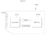
- FIG. 7 is a schematic diagram illustrating a representation of an example of a memory card system 4100 including the non-volatile memory apparatuses 1 and/or 5 in accordance with various embodiments of the present disclosure.
- the memory card system 4100 may include a controller 4110 , a memory 4120 , and an interface member 4130 .
- the controller 4110 and the memory 4120 may be configured to exchange a command and/or data.
- the memory 4120 may be used to store a command, which is executed by the controller 4110 , and/or user data.
- the memory card system 4100 may store data into the memory 4120 or output data to an external from the memory 4120 .
- the memory 4120 may include the non-volatile memory apparatuses 1 and/or 5 in accordance with various embodiments of the present disclosure.
- the interface member 4130 may be configured to transfer data from/to an external.
- the memory card system 4100 may be a multimedia card (MMC), a secure digital card (SD) or a portable data storage device.
- FIG. 8 is a block diagram illustrating a representation of an example of an electronic device 4200 including the non-volatile memory apparatuses 1 and/or 5 in accordance with various embodiments of the present disclosure.
- the electronic device 4200 may include a processor 4210 , a memory 4220 and an input and output (input/output) device 4230 .
- the processor 4210 , the memory 4220 , and the input/output device 4230 may be coupled to one another through a bus 4246 .
- the memory 4220 may receive a control signal from the processor 4210 .
- the memory 4220 may be used to store code and data for the operation of the processor 4210 .
- the memory 4220 may be used to store data, which is accessed through the bus 4246 .
- the memory 4220 may include the non-volatile memory apparatuses 1 and/or 5 in accordance with various embodiments of the present disclosure. Additional circuits and control signals may be provided for implementations and modifications of the present disclosure.
- the electronic device 4200 may be included in various electronic control devices requiring the memory 4220 .
- the electronic device 4200 may be used in a personal digital assistant (PDA), a laptop computer, a portable computer, a web tablet, a wireless phone, a portable phone, a digital music player, a MP3 player, a navigation, a solid state drive (SSD), a household appliance, or any device capable of wireless communication.
- PDA personal digital assistant
- laptop computer a portable computer
- a web tablet a wireless phone
- portable phone a portable phone
- a digital music player a digital music player
- MP3 player digital music player
- SSD solid state drive
- household appliance or any device capable of wireless communication.
- FIG. 9 is a block diagram illustrating a representation of an example of a data storage device including the non-volatile memory apparatuses 1 and/or 5 in accordance with various embodiments of the present disclosure.
- a data storage device may be provided such as the solid state drive (SSD: 4311 ).
- the SSD 4311 may include an interface 4313 , a controller 4315 , a non-volatile memory 4318 , and a buffer memory 4319 .
- the SSD 4311 stores data through a semiconductor device.
- the SSD 4311 has an advantage over the hard disk drive (HDD) since the SSD 4311 operates faster and is friendly to miniaturization and weight-lightening while having low mechanical delay or failure rate, low heating and low noise.
- the SSD 4311 may be widely used in a notebook PC, a netbook, a desktop PC, a MP3 player, or a portable storage device.
- the controller 4315 may be disposed near to the interface 4313 and may be electrically coupled to the interface 4313 .
- the controller 4315 may be a microprocessor including a memory controller and a buffer controller.
- the non-volatile memory 4318 may be disposed near the controller 4315 and may be electrically coupled to the controller 4315 through a connection terminal T. Data storage capacity of the SSD 4311 may correspond to that of the non-volatile memory 4318 .
- the buffer memory 4319 may be disposed near the controller 4315 and may be electrically coupled to the controller 4315 .
- the interface 4313 may be coupled to a host 4302 and configured to transfer an electrical signal such as data.
- the interface 4313 may conform to a protocol such as the serial advanced technology attachment (SATA), the integrated drive electronics (IDE), the small computer system interface (SCSI), and/or combination thereof.
- SATA serial advanced technology attachment
- IDE integrated drive electronics
- SCSI small computer system interface
- the non-volatile memory 4318 may be coupled to the interface 4313 through the controller 4315 .
- the non-volatile memory 4318 may store data provided through the interface 4313 .
- the non-volatile memory 4318 may include the non-volatile memory apparatuses 1 and/or 5 in accordance with various embodiments of the present disclosure.
- the non-volatile memory 4318 may maintain stored data even when power supply to the SSD 4311 is cut off.
- the buffer memory 4319 may include a volatile memory.
- the volatile memory may be the dynamic random-access memory (DRAM) and/or the static RAM (SRAM).
- the buffer memory 4319 may operate faster than the non-volatile memory 4318 .
- the interface 4313 may process data faster than the non-volatile memory 4318 .
- the buffer memory 4319 may temporarily store data. Data provided through the interface 4313 may be temporarily stored in the buffer memory 4319 via the controller 4315 , and may be stored in the non-volatile memory 4318 at the data storage speed of the non-volatile memory 4318 .
- frequently accessed data may be read in advance from the non-volatile memory 4318 and temporarily stored in the buffer memory 4319 . That is, the buffer memory 4319 may serve to increase effective operation speed of the SSD 4311 and reduce error rate of the SSD 4311 .
- FIG. 10 is a block diagram illustrating a representation of an example of an electronic system 4400 including the non-volatile memory apparatuses 1 and/or 5 in accordance with various embodiments of the present disclosure.
- the electronic system 4400 may include a body 4410 .
- a microprocessor unit 4420 a power unit 4430 , a function unit 4440 , and a display controller unit 4450 .
- the body 4410 may be a motherboard formed with the printed circuit board (PCB).
- the microprocessor unit 4420 , the power unit 4430 , the function unit 4440 , and the display controller unit 4450 may be mounted on the body 4410 .
- a display unit 4460 may be disposed in or outside the body 4410 .
- the display unit 4460 may be disposed on a surface of the body 4410 and display image processed by the display controller unit 4450 .
- the power unit 4430 may receive a predetermined voltage from an external battery, divide the provided voltage into required voltages of various levels, and provide the divided voltages to the microprocessor unit 4420 , the function unit 4440 , the display controller unit 4450 and so forth.
- the microprocessor unit 4420 may receive the divided voltage from the power unit 4430 and may control the function unit 4440 and the display unit 4460 .
- the function unit 4440 may perform various functions of the electronic system 4400 .
- the function unit 4440 may include various element capable of cellular phone functions such as dialling, image output to the display unit 4460 and voice output to a speaker through communication with an external device 4470 and so forth, and may function as a camera image processor when a camera is mounted in the electronic system 4400 .
- the function unit 4440 may be a memory card controller.
- the function unit 4440 may exchange signals with the external device 4470 through a wired or wireless communication unit 4480 .
- the function unit 4440 may work as an interface controller.
- the non-volatile memory apparatuses 1 and/or 5 in accordance with various embodiments of the present disclosure may be applied to one or more of the microprocessor unit 4420 and the function unit 4440 .
- non-volatile memory apparatus should not be limited based on the described embodiments. Rather, the non-volatile memory apparatus described herein should only be limited in light of the claims that follow when taken in conjunction with the above description and accompanying drawings.
Landscapes
- Semiconductor Memories (AREA)
- Read Only Memory (AREA)
- Chemical & Material Sciences (AREA)
- Crystallography & Structural Chemistry (AREA)
Priority Applications (1)
| Application Number | Priority Date | Filing Date | Title |
|---|---|---|---|
| US16/521,221 US10497439B1 (en) | 2016-12-02 | 2019-07-24 | Non-volatile memory apparatus including voltage clamping circuit |
Applications Claiming Priority (2)
| Application Number | Priority Date | Filing Date | Title |
|---|---|---|---|
| KR1020160163803A KR102657562B1 (ko) | 2016-12-02 | 2016-12-02 | 비휘발성 메모리 장치 |
| KR10-2016-0163803 | 2016-12-02 |
Related Child Applications (1)
| Application Number | Title | Priority Date | Filing Date |
|---|---|---|---|
| US16/521,221 Division US10497439B1 (en) | 2016-12-02 | 2019-07-24 | Non-volatile memory apparatus including voltage clamping circuit |
Publications (2)
| Publication Number | Publication Date |
|---|---|
| US20180158524A1 US20180158524A1 (en) | 2018-06-07 |
| US10403356B2 true US10403356B2 (en) | 2019-09-03 |
Family
ID=62244040
Family Applications (2)
| Application Number | Title | Priority Date | Filing Date |
|---|---|---|---|
| US15/814,625 Active US10403356B2 (en) | 2016-12-02 | 2017-11-16 | Non-volatile memory apparatus including voltage clamping circuit |
| US16/521,221 Active US10497439B1 (en) | 2016-12-02 | 2019-07-24 | Non-volatile memory apparatus including voltage clamping circuit |
Family Applications After (1)
| Application Number | Title | Priority Date | Filing Date |
|---|---|---|---|
| US16/521,221 Active US10497439B1 (en) | 2016-12-02 | 2019-07-24 | Non-volatile memory apparatus including voltage clamping circuit |
Country Status (4)
| Country | Link |
|---|---|
| US (2) | US10403356B2 (zh) |
| KR (1) | KR102657562B1 (zh) |
| CN (1) | CN108154897B (zh) |
| TW (1) | TWI738926B (zh) |
Families Citing this family (9)
| Publication number | Priority date | Publication date | Assignee | Title |
|---|---|---|---|---|
| KR20190042892A (ko) | 2017-10-17 | 2019-04-25 | 에스케이하이닉스 주식회사 | 반도체 메모리 장치 및 이의 동작 방법 |
| KR102401183B1 (ko) * | 2017-12-05 | 2022-05-24 | 삼성전자주식회사 | 메모리 장치 및 그 동작 방법 |
| KR102501696B1 (ko) * | 2018-06-18 | 2023-02-21 | 에스케이하이닉스 주식회사 | 전압 클램핑 회로, 이를 포함하는 반도체 장치 및 반도체 시스템 |
| KR102515463B1 (ko) * | 2018-06-18 | 2023-03-30 | 에스케이하이닉스 주식회사 | 비휘발성 메모리 장치와, 이의 리드 및 라이트 방법 |
| US10832765B2 (en) * | 2018-06-29 | 2020-11-10 | Taiwan Semiconductor Manufacturing Co., Ltd. | Variation tolerant read assist circuit for SRAM |
| US11437090B2 (en) * | 2018-07-16 | 2022-09-06 | Arm Limited | Negative differential resistance circuits |
| KR20200117374A (ko) * | 2019-04-04 | 2020-10-14 | 에스케이하이닉스 주식회사 | 비휘발성 메모리 장치, 이의 동작 방법 및 이를 이용하는 시스템 |
| KR20200141887A (ko) * | 2019-06-11 | 2020-12-21 | 에스케이하이닉스 주식회사 | 읽기 동작을 제어하는 제어회로를 포함하는 반도체 메모리 장치 |
| KR20210105187A (ko) * | 2020-02-18 | 2021-08-26 | 에스케이하이닉스 주식회사 | 전압 생성 회로 및 이를 이용하는 비휘발성 메모리 장치 |
Citations (7)
| Publication number | Priority date | Publication date | Assignee | Title |
|---|---|---|---|---|
| US7251163B2 (en) | 2004-06-23 | 2007-07-31 | Samsung Electronics Co., Ltd. | Flash memory device including bit line voltage clamp circuit for controlling bit line voltage during programming, and bit line voltage control method thereof |
| US20080266942A1 (en) | 2007-04-30 | 2008-10-30 | Samsung Electronics Co., Ltd. | Multiple level cell phase-change memory device having pre-reading operation resistance drift recovery, memory systems employing such devices and methods of reading memory devices |
| US20100118593A1 (en) * | 2005-08-10 | 2010-05-13 | Samsung Electronics Co., Ltd. | Variable resistance memory device and system thereof |
| US20120033489A1 (en) * | 2010-08-03 | 2012-02-09 | Samsung Electronics Co., Ltd. | Memory device, precharge controlling method thereof, and devices having the same |
| US20120075913A1 (en) * | 2010-09-24 | 2012-03-29 | Kabushiki Kaisha Toshiba | Non-volatile semiconductor memory device |
| US8467245B2 (en) | 2010-03-24 | 2013-06-18 | Ememory Technology Inc. | Non-volatile memory device with program current clamp and related method |
| KR20140090879A (ko) | 2013-01-10 | 2014-07-18 | 삼성전자주식회사 | 불휘발성 메모리 장치 및 그것의 읽기 방법 |
Family Cites Families (8)
| Publication number | Priority date | Publication date | Assignee | Title |
|---|---|---|---|---|
| KR100541816B1 (ko) * | 2003-09-19 | 2006-01-10 | 삼성전자주식회사 | 반도체 메모리에서의 데이터 리드 회로 및 데이터 리드 방법 |
| WO2008105155A1 (ja) * | 2007-02-23 | 2008-09-04 | Panasonic Corporation | 不揮発性メモリ装置、および不揮発性メモリ装置におけるデータ書込方法 |
| JP4579965B2 (ja) * | 2007-12-19 | 2010-11-10 | パナソニック株式会社 | 半導体記憶装置 |
| KR20090126587A (ko) * | 2008-06-04 | 2009-12-09 | 삼성전자주식회사 | 상 변화 메모리 장치 및 그것의 읽기 방법 |
| TW201207852A (en) * | 2010-04-05 | 2012-02-16 | Mosaid Technologies Inc | Semiconductor memory device having a three-dimensional structure |
| KR102055375B1 (ko) * | 2013-01-14 | 2020-01-22 | 삼성전자 주식회사 | 저항체를 이용한 비휘발성 메모리 장치 및 이를 포함하는 메모리 시스템 |
| WO2015179537A1 (en) * | 2014-05-20 | 2015-11-26 | Sandisk 3D Llc | Intrinsic vertical bit line architecture |
| US9530512B2 (en) * | 2014-09-19 | 2016-12-27 | Sandisk Technologies Llc | Temperature dependent sensing scheme to counteract cross-temperature threshold voltage distribution widening |
-
2016
- 2016-12-02 KR KR1020160163803A patent/KR102657562B1/ko active IP Right Grant
-
2017
- 2017-11-16 US US15/814,625 patent/US10403356B2/en active Active
- 2017-11-23 TW TW106140827A patent/TWI738926B/zh active
- 2017-11-30 CN CN201711236405.5A patent/CN108154897B/zh active Active
-
2019
- 2019-07-24 US US16/521,221 patent/US10497439B1/en active Active
Patent Citations (9)
| Publication number | Priority date | Publication date | Assignee | Title |
|---|---|---|---|---|
| US7251163B2 (en) | 2004-06-23 | 2007-07-31 | Samsung Electronics Co., Ltd. | Flash memory device including bit line voltage clamp circuit for controlling bit line voltage during programming, and bit line voltage control method thereof |
| US20100118593A1 (en) * | 2005-08-10 | 2010-05-13 | Samsung Electronics Co., Ltd. | Variable resistance memory device and system thereof |
| US8143653B2 (en) * | 2005-08-10 | 2012-03-27 | Samsung Electronics Co., Ltd. | Variable resistance memory device and system thereof |
| US20080266942A1 (en) | 2007-04-30 | 2008-10-30 | Samsung Electronics Co., Ltd. | Multiple level cell phase-change memory device having pre-reading operation resistance drift recovery, memory systems employing such devices and methods of reading memory devices |
| US8467245B2 (en) | 2010-03-24 | 2013-06-18 | Ememory Technology Inc. | Non-volatile memory device with program current clamp and related method |
| US20120033489A1 (en) * | 2010-08-03 | 2012-02-09 | Samsung Electronics Co., Ltd. | Memory device, precharge controlling method thereof, and devices having the same |
| US8861264B2 (en) * | 2010-08-03 | 2014-10-14 | Samsung Electronics Co., Ltd. | Memory device, precharge controlling method thereof, and devices having the same |
| US20120075913A1 (en) * | 2010-09-24 | 2012-03-29 | Kabushiki Kaisha Toshiba | Non-volatile semiconductor memory device |
| KR20140090879A (ko) | 2013-01-10 | 2014-07-18 | 삼성전자주식회사 | 불휘발성 메모리 장치 및 그것의 읽기 방법 |
Also Published As
| Publication number | Publication date |
|---|---|
| US10497439B1 (en) | 2019-12-03 |
| KR20180063956A (ko) | 2018-06-14 |
| CN108154897B (zh) | 2021-08-03 |
| US20190348113A1 (en) | 2019-11-14 |
| KR102657562B1 (ko) | 2024-04-17 |
| CN108154897A (zh) | 2018-06-12 |
| TWI738926B (zh) | 2021-09-11 |
| US20180158524A1 (en) | 2018-06-07 |
| TW201822197A (zh) | 2018-06-16 |
Similar Documents
| Publication | Publication Date | Title |
|---|---|---|
| US10497439B1 (en) | Non-volatile memory apparatus including voltage clamping circuit | |
| US9972366B2 (en) | Sense amplifier for high speed sensing, memory apparatus and system including the same | |
| US10861505B2 (en) | Nonvolatile memory apparatus for mitigating snap-back disturbance, and read and write method of the nonvolatile memory apparatus | |
| US10482971B2 (en) | Semiconductor memory apparatus and operating method of the semiconductor memory apparatus | |
| US20180358085A1 (en) | Semiconductor memory apparatus and operating method thereof | |
| US11024377B2 (en) | Nonvolatile memory apparatus for performing a read operation and a method of operating the same | |
| US10726915B2 (en) | Semiconductor memory apparatus, semiconductor system and electronic device including the semiconductor memory apparatus | |
| US11443801B2 (en) | Semiconductor memory apparatus for preventing disturbance | |
| US10079045B2 (en) | Sense amplifier, memory apparatus and system including the same | |
| US9997243B2 (en) | Sense amplifier, and nonvolatile memory device and system including the same | |
| US10083750B2 (en) | Semiconductor memory apparatus for adjusting voltage level of global word line, and operating method thereof | |
| US9984749B2 (en) | Current driver, write driver, and semiconductor memory apparatus using the same | |
| US11189324B2 (en) | Voltage generating circuit and a nonvolatile memory apparatus using the voltage generating circuit |
Legal Events
| Date | Code | Title | Description |
|---|---|---|---|
| AS | Assignment |
Owner name: SK HYNIX INC., KOREA, REPUBLIC OF Free format text: ASSIGNMENT OF ASSIGNORS INTEREST;ASSIGNORS:SHIN, MIN CHUL;EM, HO SEOK;REEL/FRAME:044150/0023 Effective date: 20171102 |
|
| FEPP | Fee payment procedure |
Free format text: ENTITY STATUS SET TO UNDISCOUNTED (ORIGINAL EVENT CODE: BIG.); ENTITY STATUS OF PATENT OWNER: LARGE ENTITY |
|
| STPP | Information on status: patent application and granting procedure in general |
Free format text: NON FINAL ACTION MAILED |
|
| STPP | Information on status: patent application and granting procedure in general |
Free format text: RESPONSE TO NON-FINAL OFFICE ACTION ENTERED AND FORWARDED TO EXAMINER |
|
| STPP | Information on status: patent application and granting procedure in general |
Free format text: NOTICE OF ALLOWANCE MAILED -- APPLICATION RECEIVED IN OFFICE OF PUBLICATIONS |
|
| STPP | Information on status: patent application and granting procedure in general |
Free format text: PUBLICATIONS -- ISSUE FEE PAYMENT RECEIVED |
|
| STPP | Information on status: patent application and granting procedure in general |
Free format text: PUBLICATIONS -- ISSUE FEE PAYMENT VERIFIED |
|
| STCF | Information on status: patent grant |
Free format text: PATENTED CASE |
|
| MAFP | Maintenance fee payment |
Free format text: PAYMENT OF MAINTENANCE FEE, 4TH YEAR, LARGE ENTITY (ORIGINAL EVENT CODE: M1551); ENTITY STATUS OF PATENT OWNER: LARGE ENTITY Year of fee payment: 4 |