US10325784B2 - Method for manufacturing an encapsulation cover for an electronic package and electronic package comprising a cover - Google Patents

Method for manufacturing an encapsulation cover for an electronic package and electronic package comprising a cover Download PDF

Info

Publication number
US10325784B2
US10325784B2 US15/685,552 US201715685552A US10325784B2 US 10325784 B2 US10325784 B2 US 10325784B2 US 201715685552 A US201715685552 A US 201715685552A US 10325784 B2 US10325784 B2 US 10325784B2
Authority
US
United States
Prior art keywords
substrate
insert
face
adhesive
mold
Prior art date
Legal status (The legal status is an assumption and is not a legal conclusion. Google has not performed a legal analysis and makes no representation as to the accuracy of the status listed.)
Active
Application number
US15/685,552
Other versions
US20180190512A1 (en
Inventor
Benoit Besancon
Alexandre Mas
Karine Saxod
Current Assignee (The listed assignees may be inaccurate. Google has not performed a legal analysis and makes no representation or warranty as to the accuracy of the list.)
STMicroelectronics Grenoble 2 SAS
Original Assignee
STMicroelectronics Grenoble 2 SAS
Priority date (The priority date is an assumption and is not a legal conclusion. Google has not performed a legal analysis and makes no representation as to the accuracy of the date listed.)
Filing date
Publication date
Application filed by STMicroelectronics Grenoble 2 SAS filed Critical STMicroelectronics Grenoble 2 SAS
Assigned to STMICROELECTRONICS (GRENOBLE 2) SAS reassignment STMICROELECTRONICS (GRENOBLE 2) SAS ASSIGNMENT OF ASSIGNORS INTEREST (SEE DOCUMENT FOR DETAILS). Assignors: Saxod, Karine, BESANCON, BENOIT, MAS, ALEXANDRE
Publication of US20180190512A1 publication Critical patent/US20180190512A1/en
Priority to US16/394,925 priority Critical patent/US11114312B2/en
Application granted granted Critical
Publication of US10325784B2 publication Critical patent/US10325784B2/en
Active legal-status Critical Current
Anticipated expiration legal-status Critical

Links

Images

Classifications

    • HELECTRICITY
    • H01ELECTRIC ELEMENTS
    • H01LSEMICONDUCTOR DEVICES NOT COVERED BY CLASS H10
    • H01L21/00Processes or apparatus adapted for the manufacture or treatment of semiconductor or solid state devices or of parts thereof
    • H01L21/02Manufacture or treatment of semiconductor devices or of parts thereof
    • H01L21/04Manufacture or treatment of semiconductor devices or of parts thereof the devices having at least one potential-jump barrier or surface barrier, e.g. PN junction, depletion layer or carrier concentration layer
    • H01L21/50Assembly of semiconductor devices using processes or apparatus not provided for in a single one of the subgroups H01L21/06 - H01L21/326, e.g. sealing of a cap to a base of a container
    • H01L21/56Encapsulations, e.g. encapsulation layers, coatings
    • H01L21/565Moulds
    • HELECTRICITY
    • H01ELECTRIC ELEMENTS
    • H01LSEMICONDUCTOR DEVICES NOT COVERED BY CLASS H10
    • H01L21/00Processes or apparatus adapted for the manufacture or treatment of semiconductor or solid state devices or of parts thereof
    • H01L21/02Manufacture or treatment of semiconductor devices or of parts thereof
    • H01L21/04Manufacture or treatment of semiconductor devices or of parts thereof the devices having at least one potential-jump barrier or surface barrier, e.g. PN junction, depletion layer or carrier concentration layer
    • H01L21/48Manufacture or treatment of parts, e.g. containers, prior to assembly of the devices, using processes not provided for in a single one of the subgroups H01L21/06 - H01L21/326
    • H01L21/4803Insulating or insulated parts, e.g. mountings, containers, diamond heatsinks
    • HELECTRICITY
    • H01ELECTRIC ELEMENTS
    • H01LSEMICONDUCTOR DEVICES NOT COVERED BY CLASS H10
    • H01L21/00Processes or apparatus adapted for the manufacture or treatment of semiconductor or solid state devices or of parts thereof
    • H01L21/02Manufacture or treatment of semiconductor devices or of parts thereof
    • H01L21/04Manufacture or treatment of semiconductor devices or of parts thereof the devices having at least one potential-jump barrier or surface barrier, e.g. PN junction, depletion layer or carrier concentration layer
    • H01L21/50Assembly of semiconductor devices using processes or apparatus not provided for in a single one of the subgroups H01L21/06 - H01L21/326, e.g. sealing of a cap to a base of a container
    • H01L21/52Mounting semiconductor bodies in containers
    • HELECTRICITY
    • H01ELECTRIC ELEMENTS
    • H01LSEMICONDUCTOR DEVICES NOT COVERED BY CLASS H10
    • H01L23/00Details of semiconductor or other solid state devices
    • H01L23/02Containers; Seals
    • H01L23/04Containers; Seals characterised by the shape of the container or parts, e.g. caps, walls
    • H01L23/053Containers; Seals characterised by the shape of the container or parts, e.g. caps, walls the container being a hollow construction and having an insulating or insulated base as a mounting for the semiconductor body
    • HELECTRICITY
    • H01ELECTRIC ELEMENTS
    • H01LSEMICONDUCTOR DEVICES NOT COVERED BY CLASS H10
    • H01L23/00Details of semiconductor or other solid state devices
    • H01L23/02Containers; Seals
    • H01L23/06Containers; Seals characterised by the material of the container or its electrical properties
    • HELECTRICITY
    • H01ELECTRIC ELEMENTS
    • H01LSEMICONDUCTOR DEVICES NOT COVERED BY CLASS H10
    • H01L23/00Details of semiconductor or other solid state devices
    • H01L23/02Containers; Seals
    • H01L23/10Containers; Seals characterised by the material or arrangement of seals between parts, e.g. between cap and base of the container or between leads and walls of the container
    • HELECTRICITY
    • H01ELECTRIC ELEMENTS
    • H01LSEMICONDUCTOR DEVICES NOT COVERED BY CLASS H10
    • H01L23/00Details of semiconductor or other solid state devices
    • H01L23/16Fillings or auxiliary members in containers or encapsulations, e.g. centering rings
    • H01L23/18Fillings characterised by the material, its physical or chemical properties, or its arrangement within the complete device
    • H01L23/24Fillings characterised by the material, its physical or chemical properties, or its arrangement within the complete device solid or gel at the normal operating temperature of the device
    • HELECTRICITY
    • H01ELECTRIC ELEMENTS
    • H01LSEMICONDUCTOR DEVICES NOT COVERED BY CLASS H10
    • H01L23/00Details of semiconductor or other solid state devices
    • H01L23/28Encapsulations, e.g. encapsulating layers, coatings, e.g. for protection
    • H01L23/31Encapsulations, e.g. encapsulating layers, coatings, e.g. for protection characterised by the arrangement or shape
    • H01L23/3107Encapsulations, e.g. encapsulating layers, coatings, e.g. for protection characterised by the arrangement or shape the device being completely enclosed
    • H01L23/315Encapsulations, e.g. encapsulating layers, coatings, e.g. for protection characterised by the arrangement or shape the device being completely enclosed the encapsulation having a cavity
    • HELECTRICITY
    • H01ELECTRIC ELEMENTS
    • H01LSEMICONDUCTOR DEVICES NOT COVERED BY CLASS H10
    • H01L23/00Details of semiconductor or other solid state devices
    • H01L23/28Encapsulations, e.g. encapsulating layers, coatings, e.g. for protection
    • H01L23/31Encapsulations, e.g. encapsulating layers, coatings, e.g. for protection characterised by the arrangement or shape
    • H01L23/3157Partial encapsulation or coating
    • H01L23/3192Multilayer coating
    • HELECTRICITY
    • H01ELECTRIC ELEMENTS
    • H01LSEMICONDUCTOR DEVICES NOT COVERED BY CLASS H10
    • H01L23/00Details of semiconductor or other solid state devices
    • H01L23/34Arrangements for cooling, heating, ventilating or temperature compensation ; Temperature sensing arrangements
    • H01L23/42Fillings or auxiliary members in containers or encapsulations selected or arranged to facilitate heating or cooling
    • H01L23/433Auxiliary members in containers characterised by their shape, e.g. pistons
    • H01L23/4334Auxiliary members in encapsulations
    • HELECTRICITY
    • H01ELECTRIC ELEMENTS
    • H01LSEMICONDUCTOR DEVICES NOT COVERED BY CLASS H10
    • H01L23/00Details of semiconductor or other solid state devices
    • H01L23/552Protection against radiation, e.g. light or electromagnetic waves
    • HELECTRICITY
    • H01ELECTRIC ELEMENTS
    • H01LSEMICONDUCTOR DEVICES NOT COVERED BY CLASS H10
    • H01L2224/00Indexing scheme for arrangements for connecting or disconnecting semiconductor or solid-state bodies and methods related thereto as covered by H01L24/00
    • H01L2224/01Means for bonding being attached to, or being formed on, the surface to be connected, e.g. chip-to-package, die-attach, "first-level" interconnects; Manufacturing methods related thereto
    • H01L2224/42Wire connectors; Manufacturing methods related thereto
    • H01L2224/47Structure, shape, material or disposition of the wire connectors after the connecting process
    • H01L2224/48Structure, shape, material or disposition of the wire connectors after the connecting process of an individual wire connector
    • H01L2224/4805Shape
    • H01L2224/4809Loop shape
    • H01L2224/48091Arched
    • HELECTRICITY
    • H01ELECTRIC ELEMENTS
    • H01LSEMICONDUCTOR DEVICES NOT COVERED BY CLASS H10
    • H01L2224/00Indexing scheme for arrangements for connecting or disconnecting semiconductor or solid-state bodies and methods related thereto as covered by H01L24/00
    • H01L2224/73Means for bonding being of different types provided for in two or more of groups H01L2224/10, H01L2224/18, H01L2224/26, H01L2224/34, H01L2224/42, H01L2224/50, H01L2224/63, H01L2224/71
    • H01L2224/732Location after the connecting process
    • H01L2224/73251Location after the connecting process on different surfaces
    • H01L2224/73265Layer and wire connectors
    • HELECTRICITY
    • H01ELECTRIC ELEMENTS
    • H01LSEMICONDUCTOR DEVICES NOT COVERED BY CLASS H10
    • H01L2224/00Indexing scheme for arrangements for connecting or disconnecting semiconductor or solid-state bodies and methods related thereto as covered by H01L24/00
    • H01L2224/93Batch processes
    • H01L2224/95Batch processes at chip-level, i.e. with connecting carried out on a plurality of singulated devices, i.e. on diced chips
    • H01L2224/97Batch processes at chip-level, i.e. with connecting carried out on a plurality of singulated devices, i.e. on diced chips the devices being connected to a common substrate, e.g. interposer, said common substrate being separable into individual assemblies after connecting

Definitions

  • the present invention relates to the field of electronic packages.
  • encapsulation covers are provided with members suited to these needs. These members are transferred onto the covers after the latter have been mounted on carrier substrates and are fixed to the covers by way of layers or beads of adhesive.
  • a method for manufacturing at least one encapsulation cover for an electronic package including at least one electronic chip.
  • the method comprises the following steps: placing at least one insert, having opposite faces, in a cavity of a mold having opposite faces, in a position such that at least part of one of the faces of the insert makes contact with at least part of one of the faces of said cavity of the mold; injecting a coating material into said cavity; and setting the coating material in order to obtain an overmolded substrate within which said insert is at least partly included, such that the encapsulation cover produced comprises at least one insert and at least a portion of said overmolded substrate.
  • the method may comprise a later step of cutting through said overmolded substrate and at a distance from said insert.
  • At least part of the other face of said insert may make contact with at least part of the other face of said cavity of the mold.
  • the mold may comprise at least one layer made of a compressible material forming at least part of at least one of said faces of said cavity, said insert bearing on this layer.
  • One of said faces of the cavity of the mold may comprise at least one zone surrounded by at least one groove, such that said overmolded substrate of the obtained cover is provided with at least one protruding ring-shaped rib corresponding to said groove of the mold, protruding with respect to one of the faces of said insert.
  • the method may comprise a later cutting step carried out through said overmolded substrate and said protruding ring-shaped rib.
  • An electronic package which comprises: a carrier substrate; at least one electronic chip having a back face fixed to a front mounting face of the carrier substrate; and an encapsulation cover of said chip, comprising a substrate that is overmolded around an insert, said cover being fixed at least above said mounting face of said carrier substrate in a position such that it extends above the chip.
  • Said encapsulation cover may be fixed above said carrier substrate by way of an annular bead of adhesive or an annular strip of adhesive, interposed between a peripheral zone of the carrier substrate and a peripheral zone of a back face of said overmolded substrate.
  • Said overmolded substrate may be provided with a ring-shaped rib surrounding said chip at a distance, the cover being fixed above said carrier substrate by way of a strip of adhesive interposed between said carrier substrate and said ring-shaped rib.
  • Said insert may have a front face that is at least partly uncovered by said overmolded substrate.
  • Said insert may have a back face that is at least partly uncovered by said overmolded substrate.
  • Said insert may comprise a portion that protrudes backwards, facing the front face of the chip.
  • Said backward-protruding portion may be connected to the front face of the chip by way of a layer of adhesive.
  • Said insert may be made of a heat conducting material.
  • Said insert may be made of a material capable of forming an electromagnetic protection screen.
  • Said insert may comprise a substrate extending in front of the chip.
  • Said insert may comprise a grating extending in front of the chip.
  • An encapsulation cover for an electronic package which comprises: an insert having opposite faces; and an overmolded substrate having opposite faces within which said insert is included, such that this insert has at least one face that is at least partly uncovered on the side of one of the faces of the overmolded substrate.
  • Said overmolded substrate may be provided with a ring-shaped rib that protrudes with respect to one of said opposite faces of said insert.
  • Said insert may have at least one back face that is at least partly uncovered.
  • Said insert may be made of a heat conducting material.
  • Said insert may be made of a material capable of forming an electromagnetic protection screen.
  • Said insert may comprise a substrate.
  • Said substrate may comprise a protruding portion.
  • Said insert may comprise a grating.
  • FIG. 1 shows a cross section of an electronic package
  • FIG. 2 shows a cross section of a mold for manufacturing an encapsulation cover for the package of FIG. 1 , in one manufacturing step;
  • FIG. 3 shows a horizontal cross section of the mold of FIG. 2 ;
  • FIG. 4 shows a cross section of the manufacturing mold of FIG. 2 , in another step of manufacturing the encapsulation cover
  • FIG. 5 shows a step of manufacturing the package of FIG. 1 , in cross section
  • FIG. 6 shows another step of manufacturing the package of FIG. 1 , in cross section
  • FIG. 7 shows a cross section of another electronic package
  • FIG. 8 shows a cross section of a mold for manufacturing an encapsulation cover for the package of FIG. 7 , in one manufacturing step
  • FIG. 9 shows a horizontal cross section of the mold of FIG. 8 , in another step of manufacturing the encapsulation cover
  • FIG. 10 shows a step of manufacturing the package of FIG. 7 , in cross section
  • FIG. 11 shows another step of manufacturing the package of FIG. 1 , in cross section
  • FIG. 12 shows a cross section of another electronic package
  • FIG. 13 shows a cross section of a mold for manufacturing an encapsulation cover for the package of FIG. 12 , in one manufacturing step
  • FIG. 14 shows a horizontal cross section of the mold of FIG. 13 , in another step of manufacturing the encapsulation cover
  • FIG. 15 shows a step of manufacturing the package of FIG. 12 , in cross section
  • FIG. 16 shows a cross section of another electronic package
  • FIG. 17 shows a horizontal cross section of the electronic package in FIG. 16 ;
  • FIG. 18 shows a cross section of another electronic package
  • FIG. 19 shows a cross section of a mold for manufacturing an encapsulation cover for the package of FIG. 18 , in one manufacturing step.
  • FIG. 1 illustrates an electronic package 1 which comprises a carrier substrate 2 , made of a dielectric material, including an integrated network of electrical connections 3 and having a back face 4 and a front mounting face 5 .
  • the outline of the carrier substrate 2 is, for example, square or rectangular.
  • the package 1 comprises an electronic chip 6 mounted above the front face 5 of the carrier substrate 2 by way of a layer of adhesive 7 interposed between the front face 5 of the carrier substrate 2 and a back face 3 a of the electronic chip 6 .
  • the chip 6 is electrically connected to the connection network 3 by way of electrical connection wires 8 connecting pads of the front face 5 of the carrier substrate 2 and pads of the front face 3 b of the chip 6 , the back face 4 of the carrier substrate 2 being provided with electrical connection pads for the external electrical connections of the package 1 .
  • the chip 6 could be mounted on the carrier substrate 2 by way of electrical connection elements, such as balls, which electrically connect the chip 6 and the electrical connection network 3 .
  • the package 1 comprises an encapsulation cover 9 for the chip 6 and electrical connection wires 8 in front of the carrier substrate 2 , the encapsulation cover 9 being located above and at a distance from the chip 6 , parallel to the carrier substrate 2 , and having an outline corresponding to that of the carrier substrate 2 .
  • the encapsulation cover 9 comprises a ring-shaped overmolded substrate 10 made of a coating material, for example a thermosetting resin, which has opposite back and front faces 11 and 12 , respectively, which are flat and parallel, and comprises an insert 13 in the form of a plate and the periphery of which is integrated and held within a through-passage 14 of the overmolded substrate 10 .
  • the insert 13 extends in front of and at a distance from the chip 6 and has, for example, a square or rectangular outline.
  • the insert 13 has back and front faces 15 and 16 , respectively, which are not covered by the overmolded substrate 10 , and which extend substantially in the plane of the back and front faces 11 and 12 of the overmolded substrate 10 .
  • the encapsulation cover 9 is fixed above the carrier substrate 2 by way of a local ring-shaped connecting spacer 17 interposed between a peripheral zone of the front face 5 of the carrier substrate 2 and a peripheral zone of the back face of the encapsulation cover 9 , the ring-shaped spacer 17 extending at a distance from the periphery of the chip 6 and the electrical connection wires 8 .
  • the spacer 17 may partially cover the back face 11 of the overmolded substrate 10 or cover the back face 11 of the overmolded substrate 10 and a peripheral portion of the back face 15 of the insert 13 .
  • the thickness of the spacer 17 determines the gap between the cover 9 and the carrier substrate 2 .
  • the spacer 17 may comprise an adhesive including spacing balls which determine a minimum gap between the cover 9 and the carrier substrate 2 .
  • the carrier substrate 2 , the cover 9 provided with the insert 13 and the spacer 17 define a sealed chamber 18 in which the chip 6 is located.
  • a local spacer 19 is interposed, the local spacer being placed at a distance from the electrical connection wires 8 .
  • the insert 13 is made of a heat conducting material, for example a metal, and the local spacer 19 is made of a heat conducting adhesive.
  • the insert 13 included in the cover 9 forms a means for dissipating the heat generated by the chip 6 to the outside via the attached local spacer 19 which forms a thermal seal.
  • the insert 13 may be made of a material capable of forming an electromagnetic protection screen between the chip 6 and the exterior.
  • the encapsulation cover 9 is the result of a wafer-scale manufacturing process which will now be described.
  • a mold 20 is obtained which comprises a lower part 21 and an upper part 22 between which a cavity 23 is formed.
  • the parts 21 and 22 of the mold 20 have faces 24 and 25 which are opposite, flat and parallel, and which delimit the cavity 23 in the direction of the thickness of the covers 9 to be obtained.
  • these opposite faces 24 and 25 are covered with layers made of a compressible material.
  • a plurality of inserts 13 is also obtained, resulting for example from cutting a substrate along parallel rows and parallel columns.
  • inserts 13 are placed on the face 24 , at respective locations in the sites E corresponding to covers 9 to be obtained, these sites E being adjacent and arranged in a square or rectangular matrix.
  • the mold 20 is closed by placing the upper part 22 above the lower part 21 .
  • the opposite faces 15 and 16 of the inserts 13 are facing the opposite faces 24 and 25 of the cavity 23 and are pressed against the aforementioned optional compressible layers. Free spaces separate the inserts 13 , these spaces straddling the rows and columns separating the adjacent sites E.
  • a coating material for example a thermosetting epoxy resin, is injected into the cavity 23 of the mold 20 and fills said free spaces, and this coating material is set.
  • the collective substrate 10 A is cut along the rows and columns delimiting the sites E in order to obtain covers 9 .
  • a collective carrier substrate 2 A is obtained which is provided, at sites E corresponding to electronic packages 1 to be obtained, with respective electronic connection networks 3 and which is provided, on its front face 5 A, with electronic chips 6 at respective locations in the sites E and with electrical connection wires 8 , these sites E being adjacent and arranged in a square or rectangular matrix.
  • the overmolded collective substrate 10 A is placed on top of the beads of adhesive 17 A and the blobs of adhesive corresponding to local spacers 19 and the adhesive is set so as to fix the collective substrate 10 A above the collective carrier substrate 2 A and the inserts 13 above the chips 6 .
  • the assembly formed is cut along rows and columns separating the sites E, perpendicularly to the collective substrates 2 A and 10 A and through the beads of adhesive 17 A, between and at a distance from the inserts 13 .
  • a plurality of electronic packages 1 , produced at the sites E, is then obtained, in each one of which the carrier substrate 2 is a portion of the collective carrier substrate 2 A, the cover 9 comprises an overmolded substrate 10 formed by a portion of the overmolded collective substrate 10 A, including an insert 13 , and the connecting spacer 17 is a portion of the collective beads of set adhesive 17 A, the cover 9 resulting from the substrate 10 being overmolded around the insert 13 , the chip 6 and the insert 13 being connected by the local spacer 19 .
  • FIG. 7 illustrates an electronic package 26 which comprises a carrier substrate 27 including an integrated network of electrical connections 28 and provided, on a front mounting face 29 , with an electronic chip 30 , the chip 30 being connected to the electrical connection network 28 by electrical connection wires 31 .
  • the electronic package 26 comprises an encapsulation cover 32 which comprises a ring-shaped overmolded substrate 33 made of a coating material, and an insert 34 which takes the form of a plate located in front of the chip 30 and the periphery of which is integrated and held within a through-passage 35 of the overmolded substrate 33 .
  • the overmolded substrate 33 and the insert 34 have front faces 36 and 37 , respectively, located in one and the same plane parallel to the carrier substrate 27 .
  • the ring-shaped overmolded substrate 33 is provided, as one piece, with a ring-shaped rib 38 which protrudes with respect to a back face 39 of the insert 34 and which is located around and at a distance from the periphery of the chip 30 and the electrical connection wires 31 .
  • the ring-shaped rib 38 has a back face 40 which is fixed to the front face 29 of the carrier substrate 27 by way of a local ring-shaped strip of adhesive 41 .
  • the periphery of the back face 39 of the insert 34 is adjoined to a ring-shaped front face 42 of the ring-shaped rib 38 , such that the corresponding part of the ring-shaped rib 38 forms a ring-shaped spacer between the carrier substrate 27 and the insert 34 of the cover 32 .
  • a local spacer 43 is interposed between the front face 30 b of the chip 30 and the back face 39 of the insert 34 .
  • the insert 34 is made of a heat conducting material, for example a metal, and the attached local spacer 43 is made of a heat conducting adhesive.
  • the insert 34 included in the cover 32 forms a means for dissipating the heat generated by the chip 30 to the outside via the local spacer 43 .
  • the insert 34 may be made of a metal material capable of forming, in addition, an electromagnetic protection screen between the chip 56 and the exterior.
  • the encapsulation cover 32 is the result of a wafer-scale manufacturing process which will now be described.
  • a mold 44 is obtained which comprises a lower part 45 and an upper part 46 between which a cavity 47 is formed.
  • the parts 45 and 46 of the mold 44 have opposite faces 48 and 49 which delimit the cavity 47 in the direction of the thickness of the covers 32 to be obtained.
  • the face 48 of the lower part 45 of the mold 44 has adjacent sites E arranged in a matrix, corresponding to covers 32 to be obtained.
  • the face 48 has cross-shaped grooves 50 which are formed along rows and columns of the matrix forming the sites E and which are of equal depth.
  • the face 48 of the lower part 45 of the mold 44 comprises flat zones 51 which are circumscribed by corresponding portions of the grooves 50 .
  • the face 49 of the upper part 46 of the mold 44 is flat and parallel to the zones 51 of the lower part 45 of the mold 44 .
  • the flat zones 51 of the lower part 45 of the mold 44 and the face 49 of the upper part 46 of the mold 44 are covered with layers made of a compressible material.
  • a plurality of inserts 34 is also obtained.
  • inserts 34 are placed such that, when the mold is closed, the inserts 34 are interposed between the zones 51 of the lower part 45 and the face 49 of the upper part 46 of the mold 44 , respectively, at the respective sites E corresponding to covers 32 to be obtained.
  • the inserts are at a distance from one another and leave free spaces between them which communicate with the grooves 50 , the grooves being partially covered such that, in cross section, these free spaces and the grooves 50 form T-shapes.
  • an opaque coating material for example a thermosetting epoxy resin, is injected into the cavity 47 of the mold 44 and this coating material is set.
  • a collective substrate 33 A is obtained which is provided with a plurality of cross-shaped ribs 38 A at the locations of the grooves 50 and provided with inserts 34 , which inserts are integrated and held within the coating material forming the collective substrate 33 A, the latter being overmolded around the inserts 34 .
  • the collective substrate 33 A is cut along the rows and columns delimiting the sites E in order to obtain covers 32 .
  • a collective carrier substrate 27 A is obtained which is provided, at sites E corresponding to electronic packages 26 to be obtained, with respective electronic connection networks 28 and which is provided, on its front face 29 A, with electronic chips 30 at respective adjacent sites E and with electrical wires 31 .
  • the overmolded collective substrate 33 A provided with ribs 38 A and with inserts 34 , is placed so that the ribs 38 A are on top of the collective strips of adhesive 41 A and the inserts 34 are on top of the adhesive spacers 43 , and the adhesive is set so as to fix the collective substrate 33 A above the collective carrier substrate 27 A and the inserts 34 on top of the spacers 43 .
  • the assembly formed is cut along rows and columns separating the sites E, perpendicularly to the collective carrier substrate 27 A and through the overmolded collective substrate 33 A and the ribs 38 A, between and at a distance from the inserts 34 .
  • FIG. 12 illustrates an electronic package 52 which comprises a carrier substrate 53 including an integrated network of electrical connections 54 and provided, on a front mounting face 55 , with an electronic chip 56 , the chip 56 being connected to the electrical connection network 54 by electrical connection wires 56 a.
  • the electronic package 52 comprises an encapsulation cover 57 which comprises an overmolded solid substrate 58 , made of a coating material, which extends in front of and at a distance from the chip 56 and the electrical connection wires 56 a , and an insert 59 which takes the form of a plate which is inserted into a front space 60 of the overmolded substrate 58 , such that the overmolded substrate 58 has a part 58 a which covers a back face 61 of the insert 59 and a part 58 b which surrounds the periphery of the insert 59 .
  • the overmolded substrate 58 and the insert 59 have front faces 62 and 63 , respectively, located in one and the same plane parallel to the carrier substrate 53 . In this arrangement, the insert 59 does not pass through the overmolded substrate 58 .
  • the overmolded substrate 58 is provided, as one piece, with a ring-shaped rib 64 which protrudes with respect to a back face 65 of the overmolded substrate 58 and which is located around and at a distance from the periphery of the chip 56 and the electrical connection wires 56 a.
  • the ring-shaped rib 64 has a back face 66 which is fixed to the front face 55 of the carrier substrate 53 by way of a local ring-shaped strip of adhesive 67 .
  • the insert 59 may be made of a metal material capable of forming an electromagnetic protection screen between the chip 56 and the exterior.
  • the insert 59 may form a means for enhancing the dissipation of heat generated by the chip 56 to the outside.
  • the encapsulation cover 57 is the result of a wafer-scale manufacturing process which will now be described.
  • a mold 68 is obtained which comprises two parts 69 and 70 between which a cavity 71 is formed.
  • the parts 69 and 70 of the mold 68 have opposite faces 72 and 73 which delimit the cavity 71 in the direction of the thickness of the covers 57 to be obtained.
  • the face 72 of the part 69 of the mold 68 has adjacent sites E arranged in a matrix, corresponding to covers 57 to be obtained.
  • the face 72 has cross-shaped grooves 74 which are formed along rows and columns of the matrix forming the sites E and which are of equal depth.
  • the face 72 of the part 69 of the mold 68 comprises flat zones 75 which are circumscribed by corresponding portions of the grooves 74 .
  • a plurality of inserts 59 is also obtained.
  • inserts 59 are placed such that, when the mold is closed, the front faces 63 of the inserts 59 are adjoined to the face 73 of the part 70 of the mold 68 and the back faces 61 of the inserts 59 are at a distance from the zones 75 of the part 69 of the mold 68 , at the respective sites E corresponding to covers 57 to be obtained.
  • the inserts 59 are at a distance from one another by leaving free spaces between them which communicate with the grooves 74 and by leaving free spaces between the back faces 61 of the inserts 59 and the zones 75 of the face 72 of the part 69 of the mold 68 .
  • an opaque coating material for example a thermosetting epoxy resin, is injected into the cavity 71 of the mold 68 and this coating material is set.
  • a collective substrate 58 A is obtained which is provided with a plurality of cross-shaped ribs 64 A at the locations of the grooves 74 and provided with inserts 59 , which inserts are integrated and held within spaces 60 in the coating material forming the collective substrate 58 A, the latter being overmolded around the inserts 59 .
  • the collective substrate 58 A is cut along the rows and columns delimiting the sites E in order to obtain covers 57 .
  • a collective carrier substrate 53 A is obtained which is provided, at sites E corresponding to electronic packages 52 to be obtained, with respective electronic connection networks 54 and which is provided, on its front face 55 A, with electronic chips 56 at respective adjacent sites E and with electrical connection wires 56 a.
  • the overmolded collective substrate 58 A provided with ribs 64 A and with inserts 59 , is placed so that the ribs 64 A are on top of the collective strips of adhesive 67 A, and the adhesive is set so as to fix the collective substrate 58 A above the collective carrier substrate 53 A.
  • the assembly formed is cut along rows and columns separating the sites E, perpendicularly to the collective carrier substrate 53 A and through the overmolded collective substrate 58 A and the collective ribs 64 A, between and at a distance from the inserts 59 .
  • FIGS. 16 and 17 illustrate an electronic package 76 which differs from the electronic package 52 described with reference to FIG. 12 solely in that it comprises an encapsulation cover 77 the overmolded substrate 78 of which is provided with an insert 79 , taking the form of a grating, in the place of the insert 59 .
  • the overmolded substrate 78 comprises parts 78 a that are included within the openings 79 a of the insert 79 in the form of a grating.
  • the encapsulation cover 77 and the electronic package 76 may be manufactured in the same way as that which has been described above with reference to FIGS. 13 to 15 .
  • FIG. 18 illustrates an electronic package 80 which comprises a carrier substrate 81 including an integrated network of electrical connections 82 and provided, on a front mounting face 83 , with an electronic chip 84 , the chip 84 being connected to the electrical connection network 82 by electrical connection wires 85 .
  • the overmolded substrate 87 is provided with a ring-shaped rib 93 which protrudes backwards, the back face of which is fixed to the front face 83 of the carrier substrate 81 by way of a ring-shaped layer of adhesive 94 .
  • the insert 88 additionally comprises a rear portion 88 b which protrudes backwards with respect to its back face 90 , which forms a spacer.
  • This rear portion 88 b passes through the part 87 b of the overmolded substrate 87 and is located above the central part of the chip 84 .
  • the insert 88 locally passes completely through the overmolded substrate 87 .
  • the rear portion 88 b of the insert 88 has a back face 95 which makes direct contact with the front face 84 a of the chip 84 or is connected to this front face 84 a by way of a local layer of adhesive 96 .
  • part 87 a of the overmolded substrate 87 is provided with a portion 97 which protrudes backwards and which surrounds the rear portion 88 b of the insert 88 so that the back face 95 is uncovered.
  • the insert 88 is made of a heat conducting material, for example a metal, and the local layer of adhesive 96 is made of a heat conducting material.
  • the insert 88 included in the cover 86 forms a means for dissipating the heat generated by the chip 84 to the outside, via the layer of adhesive 96 , if present, its rear portion 88 b and its overmolded substrate 88 a .
  • the insert 88 may be made of a metal material capable of forming, in addition, an electromagnetic protection screen between the chip 84 and the exterior.
  • the encapsulation cover 86 is the result of a wafer-scale manufacturing process equivalent to that described above with reference to FIGS. 13 to 15 .
  • a mold 98 comprises two parts 99 and 100 forming between them a cavity 101 and having opposite faces 102 and 103 .
  • the face 102 of the part 99 has, at the sites E, zones 104 separated by cross-shaped grooves 105 straddling the rows and columns separating the sites E.
  • Inserts 88 are placed between the parts 99 and 100 of the mold 98 , in the following positions.
  • the front faces 92 of the inserts 88 bear against the flat face 103 of the part 100 of the mold 98 .
  • the back faces 95 of the protruding rear portions 88 b of the inserts 88 bear against the bottoms 106 a of the spaces 106 of the part 99 of the mold 98 .
  • Spaces are left free between the back faces 90 of the inserts 88 around the protruding rear portions 88 b and the zones 104 of the face 102 of the part 99 of the mold 98 around the spaces 106 . Free spaces are left between the periphery of the protruding rear portions 88 b of the inserts 88 and the periphery of the spaces 106 a.

Landscapes

  • Engineering & Computer Science (AREA)
  • Physics & Mathematics (AREA)
  • Microelectronics & Electronic Packaging (AREA)
  • General Physics & Mathematics (AREA)
  • Computer Hardware Design (AREA)
  • Condensed Matter Physics & Semiconductors (AREA)
  • Power Engineering (AREA)
  • Manufacturing & Machinery (AREA)
  • Health & Medical Sciences (AREA)
  • Electromagnetism (AREA)
  • Toxicology (AREA)
  • Chemical & Material Sciences (AREA)
  • Dispersion Chemistry (AREA)
  • Encapsulation Of And Coatings For Semiconductor Or Solid State Devices (AREA)
  • Injection Moulding Of Plastics Or The Like (AREA)

Abstract

A method for manufacturing a cover for an electronic package includes placing an insert having opposite faces between opposite faces of a cavity of a mold. A coating material is injected in the mold cavity around the insert. The coating material is then set to form a substrate that is overmolded around the insert and produce the cover.

Description

PRIORITY CLAIM
This application claims the priority benefit of French Application for Patent No. 1,750,048, filed on Jan. 3, 2017, the disclosure of which is hereby incorporated by reference in its entirety.
TECHNICAL FIELD
The present invention relates to the field of electronic packages.
BACKGROUND
It is known practice to produce electronic packages which comprise electronic chips mounted on carrier substrates and which comprise encapsulation covers for the chips, which covers are fixed to the carrier substrates. For specific needs, in particular optical, heat dissipation, electrical or electromagnetic needs, encapsulation covers are provided with members suited to these needs. These members are transferred onto the covers after the latter have been mounted on carrier substrates and are fixed to the covers by way of layers or beads of adhesive.
SUMMARY
According to one embodiment, a method is proposed for manufacturing at least one encapsulation cover for an electronic package including at least one electronic chip. The method comprises the following steps: placing at least one insert, having opposite faces, in a cavity of a mold having opposite faces, in a position such that at least part of one of the faces of the insert makes contact with at least part of one of the faces of said cavity of the mold; injecting a coating material into said cavity; and setting the coating material in order to obtain an overmolded substrate within which said insert is at least partly included, such that the encapsulation cover produced comprises at least one insert and at least a portion of said overmolded substrate.
The method may comprise a later step of cutting through said overmolded substrate and at a distance from said insert.
At least part of the other face of said insert may make contact with at least part of the other face of said cavity of the mold.
The mold may comprise at least one layer made of a compressible material forming at least part of at least one of said faces of said cavity, said insert bearing on this layer.
One of said faces of the cavity of the mold may comprise at least one zone surrounded by at least one groove, such that said overmolded substrate of the obtained cover is provided with at least one protruding ring-shaped rib corresponding to said groove of the mold, protruding with respect to one of the faces of said insert.
The method may comprise a later cutting step carried out through said overmolded substrate and said protruding ring-shaped rib.
An electronic package is also proposed which comprises: a carrier substrate; at least one electronic chip having a back face fixed to a front mounting face of the carrier substrate; and an encapsulation cover of said chip, comprising a substrate that is overmolded around an insert, said cover being fixed at least above said mounting face of said carrier substrate in a position such that it extends above the chip.
Said encapsulation cover may be fixed above said carrier substrate by way of an annular bead of adhesive or an annular strip of adhesive, interposed between a peripheral zone of the carrier substrate and a peripheral zone of a back face of said overmolded substrate.
Said overmolded substrate may be provided with a ring-shaped rib surrounding said chip at a distance, the cover being fixed above said carrier substrate by way of a strip of adhesive interposed between said carrier substrate and said ring-shaped rib.
Said insert may have a front face that is at least partly uncovered by said overmolded substrate.
Said insert may have a back face that is at least partly uncovered by said overmolded substrate.
Said insert may comprise a portion that protrudes backwards, facing the front face of the chip.
Said backward-protruding portion may be connected to the front face of the chip by way of a layer of adhesive.
Said insert may be made of a heat conducting material.
Said insert may be made of a material capable of forming an electromagnetic protection screen.
Said insert may comprise a substrate extending in front of the chip.
Said insert may comprise a grating extending in front of the chip.
An encapsulation cover for an electronic package is also proposed, which comprises: an insert having opposite faces; and an overmolded substrate having opposite faces within which said insert is included, such that this insert has at least one face that is at least partly uncovered on the side of one of the faces of the overmolded substrate.
Said overmolded substrate may be provided with a ring-shaped rib that protrudes with respect to one of said opposite faces of said insert.
Said insert may have at least one back face that is at least partly uncovered.
Said insert may be made of a heat conducting material.
Said insert may be made of a material capable of forming an electromagnetic protection screen.
Said insert may comprise a substrate.
Said substrate may comprise a protruding portion.
Said insert may comprise a grating.
BRIEF DESCRIPTION OF THE DRAWINGS
Electronic packages and modes of manufacture of encapsulation covers for electronic packages will now be described by way of non-limiting examples, which are illustrated by the appended drawings in which:
FIG. 1 shows a cross section of an electronic package;
FIG. 2 shows a cross section of a mold for manufacturing an encapsulation cover for the package of FIG. 1, in one manufacturing step;
FIG. 3 shows a horizontal cross section of the mold of FIG. 2;
FIG. 4 shows a cross section of the manufacturing mold of FIG. 2, in another step of manufacturing the encapsulation cover;
FIG. 5 shows a step of manufacturing the package of FIG. 1, in cross section;
FIG. 6 shows another step of manufacturing the package of FIG. 1, in cross section;
FIG. 7 shows a cross section of another electronic package;
FIG. 8 shows a cross section of a mold for manufacturing an encapsulation cover for the package of FIG. 7, in one manufacturing step;
FIG. 9 shows a horizontal cross section of the mold of FIG. 8, in another step of manufacturing the encapsulation cover;
FIG. 10 shows a step of manufacturing the package of FIG. 7, in cross section;
FIG. 11 shows another step of manufacturing the package of FIG. 1, in cross section;
FIG. 12 shows a cross section of another electronic package;
FIG. 13 shows a cross section of a mold for manufacturing an encapsulation cover for the package of FIG. 12, in one manufacturing step;
FIG. 14 shows a horizontal cross section of the mold of FIG. 13, in another step of manufacturing the encapsulation cover;
FIG. 15 shows a step of manufacturing the package of FIG. 12, in cross section;
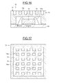
FIG. 16 shows a cross section of another electronic package;
FIG. 17 shows a horizontal cross section of the electronic package in FIG. 16;
FIG. 18 shows a cross section of another electronic package; and
FIG. 19 shows a cross section of a mold for manufacturing an encapsulation cover for the package of FIG. 18, in one manufacturing step.
DETAILED DESCRIPTION
FIG. 1 illustrates an electronic package 1 which comprises a carrier substrate 2, made of a dielectric material, including an integrated network of electrical connections 3 and having a back face 4 and a front mounting face 5. The outline of the carrier substrate 2 is, for example, square or rectangular.
The package 1 comprises an electronic chip 6 mounted above the front face 5 of the carrier substrate 2 by way of a layer of adhesive 7 interposed between the front face 5 of the carrier substrate 2 and a back face 3 a of the electronic chip 6.
The chip 6 is electrically connected to the connection network 3 by way of electrical connection wires 8 connecting pads of the front face 5 of the carrier substrate 2 and pads of the front face 3 b of the chip 6, the back face 4 of the carrier substrate 2 being provided with electrical connection pads for the external electrical connections of the package 1. According to one variant embodiment, the chip 6 could be mounted on the carrier substrate 2 by way of electrical connection elements, such as balls, which electrically connect the chip 6 and the electrical connection network 3.
The package 1 comprises an encapsulation cover 9 for the chip 6 and electrical connection wires 8 in front of the carrier substrate 2, the encapsulation cover 9 being located above and at a distance from the chip 6, parallel to the carrier substrate 2, and having an outline corresponding to that of the carrier substrate 2.
The encapsulation cover 9 comprises a ring-shaped overmolded substrate 10 made of a coating material, for example a thermosetting resin, which has opposite back and front faces 11 and 12, respectively, which are flat and parallel, and comprises an insert 13 in the form of a plate and the periphery of which is integrated and held within a through-passage 14 of the overmolded substrate 10. The insert 13 extends in front of and at a distance from the chip 6 and has, for example, a square or rectangular outline. For example, the insert 13 has back and front faces 15 and 16, respectively, which are not covered by the overmolded substrate 10, and which extend substantially in the plane of the back and front faces 11 and 12 of the overmolded substrate 10.
The encapsulation cover 9 is fixed above the carrier substrate 2 by way of a local ring-shaped connecting spacer 17 interposed between a peripheral zone of the front face 5 of the carrier substrate 2 and a peripheral zone of the back face of the encapsulation cover 9, the ring-shaped spacer 17 extending at a distance from the periphery of the chip 6 and the electrical connection wires 8. The spacer 17 may partially cover the back face 11 of the overmolded substrate 10 or cover the back face 11 of the overmolded substrate 10 and a peripheral portion of the back face 15 of the insert 13.
The thickness of the spacer 17 determines the gap between the cover 9 and the carrier substrate 2. The spacer 17 may comprise an adhesive including spacing balls which determine a minimum gap between the cover 9 and the carrier substrate 2.
Thus, the carrier substrate 2, the cover 9 provided with the insert 13 and the spacer 17 define a sealed chamber 18 in which the chip 6 is located.
Between the front face 3 b of the chip 6 and the back face 15 of the insert 13 (which extends through the overmolded substrate 10) a local spacer 19 is interposed, the local spacer being placed at a distance from the electrical connection wires 8.
According to one variant embodiment, the insert 13 is made of a heat conducting material, for example a metal, and the local spacer 19 is made of a heat conducting adhesive. Thus, the insert 13 included in the cover 9 forms a means for dissipating the heat generated by the chip 6 to the outside via the attached local spacer 19 which forms a thermal seal. In addition, the insert 13 may be made of a material capable of forming an electromagnetic protection screen between the chip 6 and the exterior.
The encapsulation cover 9 is the result of a wafer-scale manufacturing process which will now be described.
As illustrated in FIGS. 2 and 3, a mold 20 is obtained which comprises a lower part 21 and an upper part 22 between which a cavity 23 is formed. The parts 21 and 22 of the mold 20 have faces 24 and 25 which are opposite, flat and parallel, and which delimit the cavity 23 in the direction of the thickness of the covers 9 to be obtained. Optionally, these opposite faces 24 and 25 are covered with layers made of a compressible material.
A plurality of inserts 13 is also obtained, resulting for example from cutting a substrate along parallel rows and parallel columns.
With the mold 20 open, inserts 13 are placed on the face 24, at respective locations in the sites E corresponding to covers 9 to be obtained, these sites E being adjacent and arranged in a square or rectangular matrix.
Next, the mold 20 is closed by placing the upper part 22 above the lower part 21. In this position, the opposite faces 15 and 16 of the inserts 13 are facing the opposite faces 24 and 25 of the cavity 23 and are pressed against the aforementioned optional compressible layers. Free spaces separate the inserts 13, these spaces straddling the rows and columns separating the adjacent sites E.
Next, as illustrated in FIG. 4, a coating material, for example a thermosetting epoxy resin, is injected into the cavity 23 of the mold 20 and fills said free spaces, and this coating material is set.
After removal from the mold, a collective substrate 10A provided with inserts 13 and overmolded around these inserts 13 is obtained.
According to one variant embodiment, the collective substrate 10A is cut along the rows and columns delimiting the sites E in order to obtain covers 9.
According to another variant embodiment, as illustrated in FIG. 5, a collective carrier substrate 2A is obtained which is provided, at sites E corresponding to electronic packages 1 to be obtained, with respective electronic connection networks 3 and which is provided, on its front face 5A, with electronic chips 6 at respective locations in the sites E and with electrical connection wires 8, these sites E being adjacent and arranged in a square or rectangular matrix.
Next, collective beads of adhesive 17A are spread over the front face 5A of the collective carrier substrate 2A, along border zones between the sites E surrounding the central zones of the sites E in which the chips 6 are located. Local blobs of conductive adhesive are deposited on the chips 6, corresponding to local spacers 19 to be obtained.
Next, the overmolded collective substrate 10A, provided with the inserts 13, is placed on top of the beads of adhesive 17A and the blobs of adhesive corresponding to local spacers 19 and the adhesive is set so as to fix the collective substrate 10A above the collective carrier substrate 2A and the inserts 13 above the chips 6.
Next, the assembly formed is cut along rows and columns separating the sites E, perpendicularly to the collective substrates 2A and 10A and through the beads of adhesive 17A, between and at a distance from the inserts 13.
A plurality of electronic packages 1, produced at the sites E, is then obtained, in each one of which the carrier substrate 2 is a portion of the collective carrier substrate 2A, the cover 9 comprises an overmolded substrate 10 formed by a portion of the overmolded collective substrate 10A, including an insert 13, and the connecting spacer 17 is a portion of the collective beads of set adhesive 17A, the cover 9 resulting from the substrate 10 being overmolded around the insert 13, the chip 6 and the insert 13 being connected by the local spacer 19.
FIG. 7 illustrates an electronic package 26 which comprises a carrier substrate 27 including an integrated network of electrical connections 28 and provided, on a front mounting face 29, with an electronic chip 30, the chip 30 being connected to the electrical connection network 28 by electrical connection wires 31.
The electronic package 26 comprises an encapsulation cover 32 which comprises a ring-shaped overmolded substrate 33 made of a coating material, and an insert 34 which takes the form of a plate located in front of the chip 30 and the periphery of which is integrated and held within a through-passage 35 of the overmolded substrate 33. The overmolded substrate 33 and the insert 34 have front faces 36 and 37, respectively, located in one and the same plane parallel to the carrier substrate 27.
The ring-shaped overmolded substrate 33 is provided, as one piece, with a ring-shaped rib 38 which protrudes with respect to a back face 39 of the insert 34 and which is located around and at a distance from the periphery of the chip 30 and the electrical connection wires 31.
The ring-shaped rib 38 has a back face 40 which is fixed to the front face 29 of the carrier substrate 27 by way of a local ring-shaped strip of adhesive 41. In the example shown, the periphery of the back face 39 of the insert 34 is adjoined to a ring-shaped front face 42 of the ring-shaped rib 38, such that the corresponding part of the ring-shaped rib 38 forms a ring-shaped spacer between the carrier substrate 27 and the insert 34 of the cover 32.
A local spacer 43 is interposed between the front face 30 b of the chip 30 and the back face 39 of the insert 34.
According to one variant embodiment, in the same way as for the electronic package 1 described above, the insert 34 is made of a heat conducting material, for example a metal, and the attached local spacer 43 is made of a heat conducting adhesive. Thus, the insert 34 included in the cover 32 forms a means for dissipating the heat generated by the chip 30 to the outside via the local spacer 43. The insert 34 may be made of a metal material capable of forming, in addition, an electromagnetic protection screen between the chip 56 and the exterior.
The encapsulation cover 32 is the result of a wafer-scale manufacturing process which will now be described.
As illustrated in FIG. 8, a mold 44 is obtained which comprises a lower part 45 and an upper part 46 between which a cavity 47 is formed. The parts 45 and 46 of the mold 44 have opposite faces 48 and 49 which delimit the cavity 47 in the direction of the thickness of the covers 32 to be obtained.
The face 48 of the lower part 45 of the mold 44 has adjacent sites E arranged in a matrix, corresponding to covers 32 to be obtained. The face 48 has cross-shaped grooves 50 which are formed along rows and columns of the matrix forming the sites E and which are of equal depth.
Thus, at each site E, the face 48 of the lower part 45 of the mold 44 comprises flat zones 51 which are circumscribed by corresponding portions of the grooves 50.
The face 49 of the upper part 46 of the mold 44 is flat and parallel to the zones 51 of the lower part 45 of the mold 44.
Optionally, the flat zones 51 of the lower part 45 of the mold 44 and the face 49 of the upper part 46 of the mold 44 are covered with layers made of a compressible material.
A plurality of inserts 34 is also obtained.
With the mold 44 open, inserts 34 are placed such that, when the mold is closed, the inserts 34 are interposed between the zones 51 of the lower part 45 and the face 49 of the upper part 46 of the mold 44, respectively, at the respective sites E corresponding to covers 32 to be obtained. In this position, the inserts are at a distance from one another and leave free spaces between them which communicate with the grooves 50, the grooves being partially covered such that, in cross section, these free spaces and the grooves 50 form T-shapes.
Next, as illustrated in FIG. 9, an opaque coating material, for example a thermosetting epoxy resin, is injected into the cavity 47 of the mold 44 and this coating material is set.
After removal from the mold, a collective substrate 33A is obtained which is provided with a plurality of cross-shaped ribs 38A at the locations of the grooves 50 and provided with inserts 34, which inserts are integrated and held within the coating material forming the collective substrate 33A, the latter being overmolded around the inserts 34.
According to one variant embodiment, the collective substrate 33A is cut along the rows and columns delimiting the sites E in order to obtain covers 32.
According to another variant embodiment, as illustrated in FIG. 11, a collective carrier substrate 27A is obtained which is provided, at sites E corresponding to electronic packages 26 to be obtained, with respective electronic connection networks 28 and which is provided, on its front face 29A, with electronic chips 30 at respective adjacent sites E and with electrical wires 31.
Next, collective strips of adhesive 41A are spread over the front face 29A of the collective carrier substrate 27A, straddling the rows and columns separating the sites E with a view to obtaining the strips of adhesive 41 of the packages 26 to be obtained. Local blobs of conductive adhesive are deposited on the chips 30, corresponding to local spacers 43 to be obtained.
Next, the overmolded collective substrate 33A, provided with ribs 38A and with inserts 34, is placed so that the ribs 38A are on top of the collective strips of adhesive 41A and the inserts 34 are on top of the adhesive spacers 43, and the adhesive is set so as to fix the collective substrate 33A above the collective carrier substrate 27A and the inserts 34 on top of the spacers 43.
Next, the assembly formed is cut along rows and columns separating the sites E, perpendicularly to the collective carrier substrate 27A and through the overmolded collective substrate 33A and the ribs 38A, between and at a distance from the inserts 34.
A plurality of electronic packages 26, produced at the sites E, is then obtained.
FIG. 12 illustrates an electronic package 52 which comprises a carrier substrate 53 including an integrated network of electrical connections 54 and provided, on a front mounting face 55, with an electronic chip 56, the chip 56 being connected to the electrical connection network 54 by electrical connection wires 56 a.
The electronic package 52 comprises an encapsulation cover 57 which comprises an overmolded solid substrate 58, made of a coating material, which extends in front of and at a distance from the chip 56 and the electrical connection wires 56 a, and an insert 59 which takes the form of a plate which is inserted into a front space 60 of the overmolded substrate 58, such that the overmolded substrate 58 has a part 58 a which covers a back face 61 of the insert 59 and a part 58 b which surrounds the periphery of the insert 59. The overmolded substrate 58 and the insert 59 have front faces 62 and 63, respectively, located in one and the same plane parallel to the carrier substrate 53. In this arrangement, the insert 59 does not pass through the overmolded substrate 58.
In the same way as for the electrical package 26, the overmolded substrate 58 is provided, as one piece, with a ring-shaped rib 64 which protrudes with respect to a back face 65 of the overmolded substrate 58 and which is located around and at a distance from the periphery of the chip 56 and the electrical connection wires 56 a.
The ring-shaped rib 64 has a back face 66 which is fixed to the front face 55 of the carrier substrate 53 by way of a local ring-shaped strip of adhesive 67.
According to one variant embodiment, the insert 59 may be made of a metal material capable of forming an electromagnetic protection screen between the chip 56 and the exterior. In addition, the insert 59 may form a means for enhancing the dissipation of heat generated by the chip 56 to the outside.
The encapsulation cover 57 is the result of a wafer-scale manufacturing process which will now be described.
As illustrated in FIG. 13, a mold 68 is obtained which comprises two parts 69 and 70 between which a cavity 71 is formed. The parts 69 and 70 of the mold 68 have opposite faces 72 and 73 which delimit the cavity 71 in the direction of the thickness of the covers 57 to be obtained.
The face 72 of the part 69 of the mold 68 has adjacent sites E arranged in a matrix, corresponding to covers 57 to be obtained. The face 72 has cross-shaped grooves 74 which are formed along rows and columns of the matrix forming the sites E and which are of equal depth.
Thus, at each site E, the face 72 of the part 69 of the mold 68 comprises flat zones 75 which are circumscribed by corresponding portions of the grooves 74.
The face 73 of the part 70 of the mold 68 is flat and parallel to the zones 75 of the part 69 of the mold 68.
A plurality of inserts 59 is also obtained.
With the mold 68 open, inserts 59 are placed such that, when the mold is closed, the front faces 63 of the inserts 59 are adjoined to the face 73 of the part 70 of the mold 68 and the back faces 61 of the inserts 59 are at a distance from the zones 75 of the part 69 of the mold 68, at the respective sites E corresponding to covers 57 to be obtained. In this position, the inserts 59 are at a distance from one another by leaving free spaces between them which communicate with the grooves 74 and by leaving free spaces between the back faces 61 of the inserts 59 and the zones 75 of the face 72 of the part 69 of the mold 68.
Next, as illustrated in FIG. 14, an opaque coating material, for example a thermosetting epoxy resin, is injected into the cavity 71 of the mold 68 and this coating material is set.
After removal from the mold, a collective substrate 58A is obtained which is provided with a plurality of cross-shaped ribs 64A at the locations of the grooves 74 and provided with inserts 59, which inserts are integrated and held within spaces 60 in the coating material forming the collective substrate 58A, the latter being overmolded around the inserts 59.
According to one variant embodiment, the collective substrate 58A is cut along the rows and columns delimiting the sites E in order to obtain covers 57.
According to another variant embodiment, as illustrated in FIG. 15, a collective carrier substrate 53A is obtained which is provided, at sites E corresponding to electronic packages 52 to be obtained, with respective electronic connection networks 54 and which is provided, on its front face 55A, with electronic chips 56 at respective adjacent sites E and with electrical connection wires 56 a.
Collective strips of adhesive 67A are spread over the front face 55A of the collective carrier substrate 53A, straddling the rows and columns separating the sites E with a view to obtaining the strips of adhesive 67 of the packages 52 to be obtained.
Next, the overmolded collective substrate 58A, provided with ribs 64A and with inserts 59, is placed so that the ribs 64A are on top of the collective strips of adhesive 67A, and the adhesive is set so as to fix the collective substrate 58A above the collective carrier substrate 53A.
Next, the assembly formed is cut along rows and columns separating the sites E, perpendicularly to the collective carrier substrate 53A and through the overmolded collective substrate 58A and the collective ribs 64A, between and at a distance from the inserts 59.
A plurality of electronic packages 52, produced at the sites E, is then obtained.
FIGS. 16 and 17 illustrate an electronic package 76 which differs from the electronic package 52 described with reference to FIG. 12 solely in that it comprises an encapsulation cover 77 the overmolded substrate 78 of which is provided with an insert 79, taking the form of a grating, in the place of the insert 59. This time, the overmolded substrate 78 comprises parts 78 a that are included within the openings 79 a of the insert 79 in the form of a grating.
The encapsulation cover 77 and the electronic package 76 may be manufactured in the same way as that which has been described above with reference to FIGS. 13 to 15.
FIG. 18 illustrates an electronic package 80 which comprises a carrier substrate 81 including an integrated network of electrical connections 82 and provided, on a front mounting face 83, with an electronic chip 84, the chip 84 being connected to the electrical connection network 82 by electrical connection wires 85.
The electronic package 80 comprises an encapsulation cover 86 which comprises, in the same way as for the electronic package 52 described with reference to FIG. 12, an overmolded solid substrate 87, made of a coating material, which extends in front of and at a distance from the chip 84 and the electrical connection wires 85, and an insert 88 which comprises a substrate 88 a which is inserted into a front space 89 of the overmolded substrate 87, such that the overmolded substrate 87 has a part 87 a which covers a back face 90 of the substrate 88 a of the insert 88 and a part 87 b which surrounds the periphery of the insert 88. The overmolded substrate 87 and the insert 88 have front faces 91 and 92, respectively, located in one and the same plane parallel to the carrier substrate 81, such that the front face 92 of the insert 88 is uncovered.
In the same way as for the electronic package 52 described with reference to FIG. 12, the overmolded substrate 87 is provided with a ring-shaped rib 93 which protrudes backwards, the back face of which is fixed to the front face 83 of the carrier substrate 81 by way of a ring-shaped layer of adhesive 94.
In this exemplary embodiment, the insert 88 additionally comprises a rear portion 88 b which protrudes backwards with respect to its back face 90, which forms a spacer. This rear portion 88 b passes through the part 87 b of the overmolded substrate 87 and is located above the central part of the chip 84. Thus, the insert 88 locally passes completely through the overmolded substrate 87.
The rear portion 88 b of the insert 88 has a back face 95 which makes direct contact with the front face 84 a of the chip 84 or is connected to this front face 84 a by way of a local layer of adhesive 96.
In addition, the part 87 a of the overmolded substrate 87 is provided with a portion 97 which protrudes backwards and which surrounds the rear portion 88 b of the insert 88 so that the back face 95 is uncovered.
According to one variant embodiment, the insert 88 is made of a heat conducting material, for example a metal, and the local layer of adhesive 96 is made of a heat conducting material. Thus, the insert 88 included in the cover 86 forms a means for dissipating the heat generated by the chip 84 to the outside, via the layer of adhesive 96, if present, its rear portion 88 b and its overmolded substrate 88 a. The insert 88 may be made of a metal material capable of forming, in addition, an electromagnetic protection screen between the chip 84 and the exterior.
The encapsulation cover 86 is the result of a wafer-scale manufacturing process equivalent to that described above with reference to FIGS. 13 to 15.
To this end, as illustrated in FIG. 19, a mold 98 comprises two parts 99 and 100 forming between them a cavity 101 and having opposite faces 102 and 103. The face 102 of the part 99 has, at the sites E, zones 104 separated by cross-shaped grooves 105 straddling the rows and columns separating the sites E.
This time, spaces 106 are made in the zones 104 of the part 99 of the mold 98. Inserts 88 are placed between the parts 99 and 100 of the mold 98, in the following positions. The front faces 92 of the inserts 88 bear against the flat face 103 of the part 100 of the mold 98. The back faces 95 of the protruding rear portions 88 b of the inserts 88 bear against the bottoms 106 a of the spaces 106 of the part 99 of the mold 98. Spaces are left free between the back faces 90 of the inserts 88 around the protruding rear portions 88 b and the zones 104 of the face 102 of the part 99 of the mold 98 around the spaces 106. Free spaces are left between the periphery of the protruding rear portions 88 b of the inserts 88 and the periphery of the spaces 106 a.
The following steps of the wafer-scale manufacturing of the encapsulation cover 86 are equivalent to those described above with reference to FIGS. 13 to 15.
However, when assembling a collective overmolded substrate including a plurality of encapsulation covers 86, which substrate is equivalent to the collective overmolded substrate 58A, local layers of adhesive 95 should be deposited on the chips 84, which are mounted on a collective carrier substrate equivalent to the collective carrier substrate 53A, in order to connect the protruding rear portions 88 b of the inserts 88 and the front faces of the chips 84.

Claims (12)

The invention claimed is:
1. An electronic package, comprising:
a carrier substrate;
an electronic chip having a back face fixed to a front mounting face of the carrier substrate; and
an encapsulation cover comprising:
a substrate having a front face and a through passage; and
an insert which is contained within the through passage and has a front face which is coplanar with the front face of the substrate,
wherein said encapsulation cover is mounted to the front mounting face of said carrier substrate by way of an adhesive interposed between a peripheral zone of the carrier substrate and a peripheral zone of a back face of said substrate such that the insert of the encapsulation cover is positioned above a front face of the electronic chip.
2. The package according to claim 1, wherein the adhesive is an annular bead of adhesive.
3. The package according to claim 1, wherein the adhesive is an annular strip of adhesive.
4. The package according to claim 1, where said substrate includes a ring-shaped rib surrounding said electronic chip at a distance, the encapsulation cover being mounted to said front mounting face of the carrier substrate at a rear face of said ring-shaped rib.
5. The package according to claim 1, wherein said insert has a back face that is wholly covered by said substrate.
6. The package according to claim 5, wherein said insert has a back face that is at least partly uncovered by said substrate.
7. The package according to claim 6, wherein said insert comprises a portion that protrudes backwards facing the front face of the electronic chip, said portion being at least partly uncovered by said substrate.
8. The package according to claim 7, wherein said portion that protrudes backward has a surface that is mounted to the front face of the electronic chip by way of a layer of adhesive.
9. The package according to claim 1, wherein said insert is made of a heat conducting material.
10. The package according to claim 1, wherein said insert is made of a material configured to form an electromagnetic protection screen.
11. The package according to claim 1, wherein said insert comprises a substrate.
12. The package according to claim 1, wherein said insert comprises a grating.
US15/685,552 2017-01-03 2017-08-24 Method for manufacturing an encapsulation cover for an electronic package and electronic package comprising a cover Active US10325784B2 (en)

Priority Applications (1)

Application Number Priority Date Filing Date Title
US16/394,925 US11114312B2 (en) 2017-01-03 2019-04-25 Method for manufacturing an encapsulation cover for an electronic package and electronic package comprising a cover

Applications Claiming Priority (2)

Application Number Priority Date Filing Date Title
FR1750048A FR3061628A1 (en) 2017-01-03 2017-01-03 METHOD FOR MANUFACTURING AN ENCAPSULATION HOOD FOR AN ELECTRONIC HOUSING AND ELECTRONIC HOUSING COMPRISING A HOOD
FR1750048 2017-01-03

Related Child Applications (1)

Application Number Title Priority Date Filing Date
US16/394,925 Division US11114312B2 (en) 2017-01-03 2019-04-25 Method for manufacturing an encapsulation cover for an electronic package and electronic package comprising a cover

Publications (2)

Publication Number Publication Date
US20180190512A1 US20180190512A1 (en) 2018-07-05
US10325784B2 true US10325784B2 (en) 2019-06-18

Family

ID=59031037

Family Applications (2)

Application Number Title Priority Date Filing Date
US15/685,552 Active US10325784B2 (en) 2017-01-03 2017-08-24 Method for manufacturing an encapsulation cover for an electronic package and electronic package comprising a cover
US16/394,925 Active 2038-01-01 US11114312B2 (en) 2017-01-03 2019-04-25 Method for manufacturing an encapsulation cover for an electronic package and electronic package comprising a cover

Family Applications After (1)

Application Number Title Priority Date Filing Date
US16/394,925 Active 2038-01-01 US11114312B2 (en) 2017-01-03 2019-04-25 Method for manufacturing an encapsulation cover for an electronic package and electronic package comprising a cover

Country Status (2)

Country Link
US (2) US10325784B2 (en)
FR (1) FR3061628A1 (en)

Families Citing this family (4)

* Cited by examiner, † Cited by third party
Publication number Priority date Publication date Assignee Title
FR3061628A1 (en) * 2017-01-03 2018-07-06 Stmicroelectronics (Grenoble 2) Sas METHOD FOR MANUFACTURING AN ENCAPSULATION HOOD FOR AN ELECTRONIC HOUSING AND ELECTRONIC HOUSING COMPRISING A HOOD
FR3061630B1 (en) 2017-01-03 2021-07-09 St Microelectronics Grenoble 2 METHOD OF MANUFACTURING A COVER FOR AN ELECTRONIC BOX AND ELECTRONIC BOX INCLUDING A COVER
JP7219372B2 (en) * 2021-03-11 2023-02-07 積水化学工業株式会社 Coating agent preparation kit, coating agent, method for manufacturing electronic substrate and electronic component module
FR3124888A1 (en) * 2021-07-05 2023-01-06 Stmicroelectronics (Grenoble 2) Sas INTEGRATED CIRCUIT BOX

Citations (37)

* Cited by examiner, † Cited by third party
Publication number Priority date Publication date Assignee Title
JPS5818223A (en) 1981-07-28 1983-02-02 Omron Tateisi Electronics Co Molding method
US5705851A (en) * 1995-06-28 1998-01-06 National Semiconductor Corporation Thermal ball lead integrated package
FR2758908A1 (en) 1997-01-24 1998-07-31 Thomson Csf Low cost surface-mountable microwave package
US6353257B1 (en) 2000-05-19 2002-03-05 Siliconware Precision Industries Co., Ltd. Semiconductor package configuration based on lead frame having recessed and shouldered portions for flash prevention
US6414385B1 (en) 1999-11-08 2002-07-02 Siliconware Precisionindustries Co., Ltd. Quad flat non-lead package of semiconductor
US20020195701A1 (en) 2001-06-20 2002-12-26 Thomas Bemmerl Electronic component and method for producing the electronic component
US20030042596A1 (en) 2001-09-06 2003-03-06 Crane Stanford W. Semiconductor package
FR2835654A1 (en) 2002-02-06 2003-08-08 St Microelectronics Sa Optical semiconductor case with coupled lens port, comprises integrated circuit chip with optical sensor inside the case and facing the lens
US20040082114A1 (en) 2002-10-29 2004-04-29 Chih-Horng Horng Fabrication method of window-type ball grid array semiconductor package
US20050044618A1 (en) 2003-09-03 2005-03-03 Matsushita Electric Industrial Co., Ltd. Solid-state imaging device and method for manufacturing the same
US20050161755A1 (en) 2004-01-23 2005-07-28 Siliconware Precision Industries Co., Ltd. Semiconductor package with photosensitive chip and fabrication method thereof
DE102005032664A1 (en) 2005-07-13 2007-01-25 Bayer Materialscience Ag Composite component e.g. plastic window, producing method for e.g. household appliance, involves injecting synthetic material into hollow space between foils, and inserting molded part into cavity or injection molding tool
US20090086449A1 (en) 2007-09-27 2009-04-02 Masanori Minamio Optical device and manufacturing method thereof
US20090261468A1 (en) 2008-04-18 2009-10-22 Infineon Technologies Ag Semiconductor module
US20100308453A1 (en) 2009-06-03 2010-12-09 Honeywell International Inc. Integrated circuit package including a thermally and electrically conductive package lid
US20100314743A1 (en) * 2009-06-10 2010-12-16 Green Arrow Asia Limited Integrated circuit package having a castellated heatspreader
US20110049531A1 (en) 2009-08-27 2011-03-03 Mitsubishi Electric Corporation Power semiconductor device and manufacturing method for the same
EP2448001A2 (en) 2010-10-28 2012-05-02 STMicroelectronics (Grenoble 2) SAS Optical device, method for manufacturing same and electronic packaging including said optical device
US20120146243A1 (en) 2007-09-21 2012-06-14 Sungmin Song Integrated circuit packaging system with interposer
US20130079068A1 (en) 2011-09-28 2013-03-28 Stmicroelectronics (Grenoble 2) Sas Optical electronic package
US20140061447A1 (en) 2012-09-06 2014-03-06 Stmicroelectronics Pte Ltd Radiation sensor
US20150227829A1 (en) * 2008-08-29 2015-08-13 David Finn Laminates for security documents
US9472692B2 (en) 2014-12-09 2016-10-18 Stmicroelectronics (Grenoble 2) Sas Process of fabrication of electronic devices and electronic device with a double encapsulation ring
US20170127567A1 (en) 2015-10-28 2017-05-04 Stmicroelectronics (Grenoble 2) Sas Electronic device equipped with a heat sink
US20170141241A1 (en) 2015-11-17 2017-05-18 Heptagon Micro Optics Pte. Ltd. Optical Device
US9773740B2 (en) 2014-11-26 2017-09-26 Stmicroelectronics (Grenoble 2) Sas Stacked electronic device including a protective wafer bonded to a chip by an infused adhesive
US9818664B2 (en) 2016-02-26 2017-11-14 Stmicroelectronics (Grenoble 2) Sas Electronic device comprising an encapsulating block locally of smaller thickness
US9870947B1 (en) 2016-07-01 2018-01-16 Stmicroelectronics (Grenoble 2) Sas Method for collective (wafer-scale) fabrication of electronic devices and electronic device
US20180058920A1 (en) 2016-08-26 2018-03-01 Stmicroelectronics (Grenoble 2) Sas Electronic housing including a grooved cover
US20180190511A1 (en) * 2017-01-03 2018-07-05 Stmicroelectronics (Grenoble 2) Sas Method for manufacturing a cover for an electronic package and electronic package comprising a cover
US20180190838A1 (en) * 2017-01-03 2018-07-05 Stmicroelectronics (Grenoble 2) Sas Method for making a cover for an electronic package and electronic package comprising a cover
US20180190562A1 (en) 2017-01-03 2018-07-05 Stmicroelectronics (Tours) Sas Electronic device having a grooved chip
US20180190512A1 (en) * 2017-01-03 2018-07-05 Stmicroelectronics (Grenoble 2) Sas Method for manufacturing an encapsulation cover for an electronic package and electronic package comprising a cover
US20180337104A1 (en) 2017-05-16 2018-11-22 Stmicroelectronics (Grenoble 2) Sas Electronic package with a local slot forming an air-vent
US10147834B2 (en) 2015-10-16 2018-12-04 Stmicroelectronics Pte Ltd Overmold proximity sensor and associated methods
US20190027381A1 (en) 2017-07-19 2019-01-24 Toyota Jidosha Kabushiki Kaisha Method of manufacturing semiconductor device
US20190027416A1 (en) 2017-07-18 2019-01-24 Stmicroelectronics (Grenoble 2) Sas Electronic package and fabrication method

Patent Citations (38)

* Cited by examiner, † Cited by third party
Publication number Priority date Publication date Assignee Title
JPS5818223A (en) 1981-07-28 1983-02-02 Omron Tateisi Electronics Co Molding method
US5705851A (en) * 1995-06-28 1998-01-06 National Semiconductor Corporation Thermal ball lead integrated package
FR2758908A1 (en) 1997-01-24 1998-07-31 Thomson Csf Low cost surface-mountable microwave package
US6414385B1 (en) 1999-11-08 2002-07-02 Siliconware Precisionindustries Co., Ltd. Quad flat non-lead package of semiconductor
US6353257B1 (en) 2000-05-19 2002-03-05 Siliconware Precision Industries Co., Ltd. Semiconductor package configuration based on lead frame having recessed and shouldered portions for flash prevention
US20020195701A1 (en) 2001-06-20 2002-12-26 Thomas Bemmerl Electronic component and method for producing the electronic component
US20030042596A1 (en) 2001-09-06 2003-03-06 Crane Stanford W. Semiconductor package
FR2835654A1 (en) 2002-02-06 2003-08-08 St Microelectronics Sa Optical semiconductor case with coupled lens port, comprises integrated circuit chip with optical sensor inside the case and facing the lens
US20040082114A1 (en) 2002-10-29 2004-04-29 Chih-Horng Horng Fabrication method of window-type ball grid array semiconductor package
US20050044618A1 (en) 2003-09-03 2005-03-03 Matsushita Electric Industrial Co., Ltd. Solid-state imaging device and method for manufacturing the same
US20050161755A1 (en) 2004-01-23 2005-07-28 Siliconware Precision Industries Co., Ltd. Semiconductor package with photosensitive chip and fabrication method thereof
DE102005032664A1 (en) 2005-07-13 2007-01-25 Bayer Materialscience Ag Composite component e.g. plastic window, producing method for e.g. household appliance, involves injecting synthetic material into hollow space between foils, and inserting molded part into cavity or injection molding tool
US20120146243A1 (en) 2007-09-21 2012-06-14 Sungmin Song Integrated circuit packaging system with interposer
US20090086449A1 (en) 2007-09-27 2009-04-02 Masanori Minamio Optical device and manufacturing method thereof
US20090261468A1 (en) 2008-04-18 2009-10-22 Infineon Technologies Ag Semiconductor module
US20150227829A1 (en) * 2008-08-29 2015-08-13 David Finn Laminates for security documents
US20100308453A1 (en) 2009-06-03 2010-12-09 Honeywell International Inc. Integrated circuit package including a thermally and electrically conductive package lid
US20100314743A1 (en) * 2009-06-10 2010-12-16 Green Arrow Asia Limited Integrated circuit package having a castellated heatspreader
US20110049531A1 (en) 2009-08-27 2011-03-03 Mitsubishi Electric Corporation Power semiconductor device and manufacturing method for the same
US20120104454A1 (en) 2010-10-28 2012-05-03 Stmicroelectronics (Grenoble 2) Sas Optical device, process for fabricating it and an electronic package comprising this optical device
EP2448001A2 (en) 2010-10-28 2012-05-02 STMicroelectronics (Grenoble 2) SAS Optical device, method for manufacturing same and electronic packaging including said optical device
US20130079068A1 (en) 2011-09-28 2013-03-28 Stmicroelectronics (Grenoble 2) Sas Optical electronic package
US20140061447A1 (en) 2012-09-06 2014-03-06 Stmicroelectronics Pte Ltd Radiation sensor
US9773740B2 (en) 2014-11-26 2017-09-26 Stmicroelectronics (Grenoble 2) Sas Stacked electronic device including a protective wafer bonded to a chip by an infused adhesive
US9472692B2 (en) 2014-12-09 2016-10-18 Stmicroelectronics (Grenoble 2) Sas Process of fabrication of electronic devices and electronic device with a double encapsulation ring
US10147834B2 (en) 2015-10-16 2018-12-04 Stmicroelectronics Pte Ltd Overmold proximity sensor and associated methods
US20170127567A1 (en) 2015-10-28 2017-05-04 Stmicroelectronics (Grenoble 2) Sas Electronic device equipped with a heat sink
US20170141241A1 (en) 2015-11-17 2017-05-18 Heptagon Micro Optics Pte. Ltd. Optical Device
US9818664B2 (en) 2016-02-26 2017-11-14 Stmicroelectronics (Grenoble 2) Sas Electronic device comprising an encapsulating block locally of smaller thickness
US9870947B1 (en) 2016-07-01 2018-01-16 Stmicroelectronics (Grenoble 2) Sas Method for collective (wafer-scale) fabrication of electronic devices and electronic device
US20180058920A1 (en) 2016-08-26 2018-03-01 Stmicroelectronics (Grenoble 2) Sas Electronic housing including a grooved cover
US20180190511A1 (en) * 2017-01-03 2018-07-05 Stmicroelectronics (Grenoble 2) Sas Method for manufacturing a cover for an electronic package and electronic package comprising a cover
US20180190838A1 (en) * 2017-01-03 2018-07-05 Stmicroelectronics (Grenoble 2) Sas Method for making a cover for an electronic package and electronic package comprising a cover
US20180190562A1 (en) 2017-01-03 2018-07-05 Stmicroelectronics (Tours) Sas Electronic device having a grooved chip
US20180190512A1 (en) * 2017-01-03 2018-07-05 Stmicroelectronics (Grenoble 2) Sas Method for manufacturing an encapsulation cover for an electronic package and electronic package comprising a cover
US20180337104A1 (en) 2017-05-16 2018-11-22 Stmicroelectronics (Grenoble 2) Sas Electronic package with a local slot forming an air-vent
US20190027416A1 (en) 2017-07-18 2019-01-24 Stmicroelectronics (Grenoble 2) Sas Electronic package and fabrication method
US20190027381A1 (en) 2017-07-19 2019-01-24 Toyota Jidosha Kabushiki Kaisha Method of manufacturing semiconductor device

Non-Patent Citations (1)

* Cited by examiner, † Cited by third party
Title
INPI Search Report and Written Opinion for FR 1750048 dated Oct. 17, 2017 (9 pages).

Also Published As

Publication number Publication date
US20180190512A1 (en) 2018-07-05
US11114312B2 (en) 2021-09-07
US20190252212A1 (en) 2019-08-15
FR3061628A1 (en) 2018-07-06

Similar Documents

Publication Publication Date Title
US11114312B2 (en) Method for manufacturing an encapsulation cover for an electronic package and electronic package comprising a cover
US11688815B2 (en) Method for manufacturing a cover for an electronic package and electronic package comprising a cover
US9472692B2 (en) Process of fabrication of electronic devices and electronic device with a double encapsulation ring
US11552007B2 (en) Modified leadframe design with adhesive overflow recesses
US20180005889A1 (en) Method for collective (wafer-scale) fabrication of electronic devices and electronic device
US20180190511A1 (en) Method for manufacturing a cover for an electronic package and electronic package comprising a cover
JPH1174295A (en) Method for packaging electronic circuit
US20170148744A1 (en) Substrate-less integrated components
US6873039B2 (en) Methods of making microelectronic packages including electrically and/or thermally conductive element
US20220029034A1 (en) Encapsulation cover for an electronic package and fabrication process
WO2015194435A1 (en) Circuit module and method for manufacturing same
US11193821B2 (en) Ambient light sensor with light protection
TWI611555B (en) Video wall module and manufacturing method thereof
US20130107469A1 (en) Insulating Ring for Packaging, Insulating Ring Assembly and Package
US20230034445A1 (en) Electronic device comprising optical electronic components and fabricating process
JP6797234B2 (en) Semiconductor package structure and its manufacturing method
CN107924977A (en) For manufacturing the method and device of device
US20120326332A1 (en) Semiconductor device with encapsulated electrical connection elements and fabrication process thereof
US20150048504A1 (en) Package assembly for chip and method of manufacturing same
CN217588920U (en) Metal lead frame and packaging structure
US9478677B2 (en) Electronic device comprising an optical sensor chip
CN110943051A (en) Semiconductor package device and method of manufacturing the same
US9093438B2 (en) Semiconductor device package with cap element
CN109148310B (en) Electronic device comprising stacked chips
US20080311766A1 (en) Light Emitting Diode Mounting Seat and Method For Making The Same

Legal Events

Date Code Title Description
AS Assignment

Owner name: STMICROELECTRONICS (GRENOBLE 2) SAS, FRANCE

Free format text: ASSIGNMENT OF ASSIGNORS INTEREST;ASSIGNORS:BESANCON, BENOIT;MAS, ALEXANDRE;SAXOD, KARINE;SIGNING DATES FROM 20170808 TO 20170818;REEL/FRAME:043389/0498

STPP Information on status: patent application and granting procedure in general

Free format text: NOTICE OF ALLOWANCE MAILED -- APPLICATION RECEIVED IN OFFICE OF PUBLICATIONS

STPP Information on status: patent application and granting procedure in general

Free format text: AWAITING TC RESP., ISSUE FEE NOT PAID

STPP Information on status: patent application and granting procedure in general

Free format text: NOTICE OF ALLOWANCE MAILED -- APPLICATION RECEIVED IN OFFICE OF PUBLICATIONS

STCF Information on status: patent grant

Free format text: PATENTED CASE

MAFP Maintenance fee payment

Free format text: PAYMENT OF MAINTENANCE FEE, 4TH YEAR, LARGE ENTITY (ORIGINAL EVENT CODE: M1551); ENTITY STATUS OF PATENT OWNER: LARGE ENTITY

Year of fee payment: 4