US10297331B2 - Semiconductor device and electronic device - Google Patents
Semiconductor device and electronic device Download PDFInfo
- Publication number
- US10297331B2 US10297331B2 US15/333,723 US201615333723A US10297331B2 US 10297331 B2 US10297331 B2 US 10297331B2 US 201615333723 A US201615333723 A US 201615333723A US 10297331 B2 US10297331 B2 US 10297331B2
- Authority
- US
- United States
- Prior art keywords
- transistor
- gate
- electrically connected
- drain
- source
- Prior art date
- Legal status (The legal status is an assumption and is not a legal conclusion. Google has not performed a legal analysis and makes no representation as to the accuracy of the status listed.)
- Active, expires
Links
- 239000004065 semiconductor Substances 0.000 title claims abstract description 482
- 239000003990 capacitor Substances 0.000 claims description 69
- 230000002829 reductive effect Effects 0.000 abstract description 34
- 239000010410 layer Substances 0.000 description 613
- 230000006870 function Effects 0.000 description 66
- 238000000034 method Methods 0.000 description 58
- 239000000758 substrate Substances 0.000 description 57
- 239000000463 material Substances 0.000 description 48
- 239000004973 liquid crystal related substance Substances 0.000 description 46
- QVGXLLKOCUKJST-UHFFFAOYSA-N atomic oxygen Chemical compound [O] QVGXLLKOCUKJST-UHFFFAOYSA-N 0.000 description 41
- 229910052760 oxygen Inorganic materials 0.000 description 41
- 239000001301 oxygen Substances 0.000 description 41
- 239000011701 zinc Substances 0.000 description 38
- 239000010408 film Substances 0.000 description 37
- 238000005401 electroluminescence Methods 0.000 description 36
- 239000012535 impurity Substances 0.000 description 35
- 239000007789 gas Substances 0.000 description 34
- 230000015572 biosynthetic process Effects 0.000 description 33
- 238000010586 diagram Methods 0.000 description 31
- 238000010438 heat treatment Methods 0.000 description 24
- IJGRMHOSHXDMSA-UHFFFAOYSA-N Atomic nitrogen Chemical compound N#N IJGRMHOSHXDMSA-UHFFFAOYSA-N 0.000 description 22
- 125000004429 atom Chemical group 0.000 description 20
- XUIMIQQOPSSXEZ-UHFFFAOYSA-N Silicon Chemical compound [Si] XUIMIQQOPSSXEZ-UHFFFAOYSA-N 0.000 description 15
- 229920005989 resin Polymers 0.000 description 15
- 239000011347 resin Substances 0.000 description 15
- 229910052710 silicon Inorganic materials 0.000 description 15
- 239000010703 silicon Substances 0.000 description 15
- OKTJSMMVPCPJKN-UHFFFAOYSA-N Carbon Chemical compound [C] OKTJSMMVPCPJKN-UHFFFAOYSA-N 0.000 description 14
- 238000005229 chemical vapour deposition Methods 0.000 description 14
- 239000001257 hydrogen Substances 0.000 description 14
- 229910052739 hydrogen Inorganic materials 0.000 description 14
- 229910052738 indium Inorganic materials 0.000 description 14
- 238000004544 sputter deposition Methods 0.000 description 14
- 239000010409 thin film Substances 0.000 description 13
- UFHFLCQGNIYNRP-UHFFFAOYSA-N Hydrogen Chemical compound [H][H] UFHFLCQGNIYNRP-UHFFFAOYSA-N 0.000 description 12
- 229910052782 aluminium Inorganic materials 0.000 description 12
- 239000012298 atmosphere Substances 0.000 description 12
- 238000000231 atomic layer deposition Methods 0.000 description 12
- 230000000694 effects Effects 0.000 description 12
- 239000000203 mixture Substances 0.000 description 12
- 102100040862 Dual specificity protein kinase CLK1 Human genes 0.000 description 11
- XAGFODPZIPBFFR-UHFFFAOYSA-N aluminium Chemical compound [Al] XAGFODPZIPBFFR-UHFFFAOYSA-N 0.000 description 11
- 239000004020 conductor Substances 0.000 description 11
- 229910052757 nitrogen Inorganic materials 0.000 description 11
- 101000749294 Homo sapiens Dual specificity protein kinase CLK1 Proteins 0.000 description 10
- 230000008859 change Effects 0.000 description 10
- 230000005684 electric field Effects 0.000 description 10
- APFVFJFRJDLVQX-UHFFFAOYSA-N indium atom Chemical compound [In] APFVFJFRJDLVQX-UHFFFAOYSA-N 0.000 description 10
- 238000000151 deposition Methods 0.000 description 9
- 239000011810 insulating material Substances 0.000 description 9
- 230000010354 integration Effects 0.000 description 9
- 150000001875 compounds Chemical class 0.000 description 8
- 239000013078 crystal Substances 0.000 description 8
- 230000003247 decreasing effect Effects 0.000 description 8
- 230000005669 field effect Effects 0.000 description 8
- 229910052735 hafnium Inorganic materials 0.000 description 8
- 229910052751 metal Inorganic materials 0.000 description 8
- 230000004048 modification Effects 0.000 description 8
- 238000012986 modification Methods 0.000 description 8
- 239000000565 sealant Substances 0.000 description 8
- 239000000126 substance Substances 0.000 description 8
- 229910052725 zinc Inorganic materials 0.000 description 8
- PXHVJJICTQNCMI-UHFFFAOYSA-N Nickel Chemical compound [Ni] PXHVJJICTQNCMI-UHFFFAOYSA-N 0.000 description 7
- HCHKCACWOHOZIP-UHFFFAOYSA-N Zinc Chemical compound [Zn] HCHKCACWOHOZIP-UHFFFAOYSA-N 0.000 description 7
- 238000004891 communication Methods 0.000 description 7
- 230000008021 deposition Effects 0.000 description 7
- 150000004767 nitrides Chemical class 0.000 description 7
- 239000010936 titanium Substances 0.000 description 7
- 102100040858 Dual specificity protein kinase CLK4 Human genes 0.000 description 6
- 101000749298 Homo sapiens Dual specificity protein kinase CLK4 Proteins 0.000 description 6
- 239000010949 copper Substances 0.000 description 6
- PMHQVHHXPFUNSP-UHFFFAOYSA-M copper(1+);methylsulfanylmethane;bromide Chemical compound Br[Cu].CSC PMHQVHHXPFUNSP-UHFFFAOYSA-M 0.000 description 6
- 230000006866 deterioration Effects 0.000 description 6
- 238000001704 evaporation Methods 0.000 description 6
- 230000002349 favourable effect Effects 0.000 description 6
- 229910052733 gallium Inorganic materials 0.000 description 6
- VBJZVLUMGGDVMO-UHFFFAOYSA-N hafnium atom Chemical compound [Hf] VBJZVLUMGGDVMO-UHFFFAOYSA-N 0.000 description 6
- AMGQUBHHOARCQH-UHFFFAOYSA-N indium;oxotin Chemical compound [In].[Sn]=O AMGQUBHHOARCQH-UHFFFAOYSA-N 0.000 description 6
- 239000002184 metal Substances 0.000 description 6
- -1 polyethylene terephthalate Polymers 0.000 description 6
- 238000003860 storage Methods 0.000 description 6
- 238000012360 testing method Methods 0.000 description 6
- 229910052719 titanium Inorganic materials 0.000 description 6
- XLYOFNOQVPJJNP-UHFFFAOYSA-N water Substances O XLYOFNOQVPJJNP-UHFFFAOYSA-N 0.000 description 6
- RYGMFSIKBFXOCR-UHFFFAOYSA-N Copper Chemical compound [Cu] RYGMFSIKBFXOCR-UHFFFAOYSA-N 0.000 description 5
- 229910052581 Si3N4 Inorganic materials 0.000 description 5
- RTAQQCXQSZGOHL-UHFFFAOYSA-N Titanium Chemical compound [Ti] RTAQQCXQSZGOHL-UHFFFAOYSA-N 0.000 description 5
- 230000000903 blocking effect Effects 0.000 description 5
- 229910052802 copper Inorganic materials 0.000 description 5
- 230000007423 decrease Effects 0.000 description 5
- AJNVQOSZGJRYEI-UHFFFAOYSA-N digallium;oxygen(2-) Chemical compound [O-2].[O-2].[O-2].[Ga+3].[Ga+3] AJNVQOSZGJRYEI-UHFFFAOYSA-N 0.000 description 5
- 238000007667 floating Methods 0.000 description 5
- 229910001195 gallium oxide Inorganic materials 0.000 description 5
- 229910021389 graphene Inorganic materials 0.000 description 5
- 239000011261 inert gas Substances 0.000 description 5
- 239000011159 matrix material Substances 0.000 description 5
- 230000003647 oxidation Effects 0.000 description 5
- 238000007254 oxidation reaction Methods 0.000 description 5
- TWNQGVIAIRXVLR-UHFFFAOYSA-N oxo(oxoalumanyloxy)alumane Chemical compound O=[Al]O[Al]=O TWNQGVIAIRXVLR-UHFFFAOYSA-N 0.000 description 5
- 230000003071 parasitic effect Effects 0.000 description 5
- 239000002245 particle Substances 0.000 description 5
- BASFCYQUMIYNBI-UHFFFAOYSA-N platinum Chemical compound [Pt] BASFCYQUMIYNBI-UHFFFAOYSA-N 0.000 description 5
- 238000001004 secondary ion mass spectrometry Methods 0.000 description 5
- HQVNEWCFYHHQES-UHFFFAOYSA-N silicon nitride Chemical compound N12[Si]34N5[Si]62N3[Si]51N64 HQVNEWCFYHHQES-UHFFFAOYSA-N 0.000 description 5
- WFKWXMTUELFFGS-UHFFFAOYSA-N tungsten Chemical compound [W] WFKWXMTUELFFGS-UHFFFAOYSA-N 0.000 description 5
- 229910052721 tungsten Inorganic materials 0.000 description 5
- 239000010937 tungsten Substances 0.000 description 5
- XKRFYHLGVUSROY-UHFFFAOYSA-N Argon Chemical compound [Ar] XKRFYHLGVUSROY-UHFFFAOYSA-N 0.000 description 4
- 102100040844 Dual specificity protein kinase CLK2 Human genes 0.000 description 4
- 101000749291 Homo sapiens Dual specificity protein kinase CLK2 Proteins 0.000 description 4
- GWEVSGVZZGPLCZ-UHFFFAOYSA-N Titan oxide Chemical compound O=[Ti]=O GWEVSGVZZGPLCZ-UHFFFAOYSA-N 0.000 description 4
- 239000007983 Tris buffer Substances 0.000 description 4
- XLOMVQKBTHCTTD-UHFFFAOYSA-N Zinc monoxide Chemical compound [Zn]=O XLOMVQKBTHCTTD-UHFFFAOYSA-N 0.000 description 4
- 238000004364 calculation method Methods 0.000 description 4
- 229910052799 carbon Inorganic materials 0.000 description 4
- 239000000969 carrier Substances 0.000 description 4
- 230000015556 catabolic process Effects 0.000 description 4
- 238000006731 degradation reaction Methods 0.000 description 4
- 238000009792 diffusion process Methods 0.000 description 4
- KPUWHANPEXNPJT-UHFFFAOYSA-N disiloxane Chemical class [SiH3]O[SiH3] KPUWHANPEXNPJT-UHFFFAOYSA-N 0.000 description 4
- 239000005262 ferroelectric liquid crystals (FLCs) Substances 0.000 description 4
- 229910052732 germanium Inorganic materials 0.000 description 4
- GNPVGFCGXDBREM-UHFFFAOYSA-N germanium atom Chemical compound [Ge] GNPVGFCGXDBREM-UHFFFAOYSA-N 0.000 description 4
- 239000011521 glass Substances 0.000 description 4
- 229910002804 graphite Inorganic materials 0.000 description 4
- 239000010439 graphite Substances 0.000 description 4
- 229910000449 hafnium oxide Inorganic materials 0.000 description 4
- WIHZLLGSGQNAGK-UHFFFAOYSA-N hafnium(4+);oxygen(2-) Chemical compound [O-2].[O-2].[Hf+4] WIHZLLGSGQNAGK-UHFFFAOYSA-N 0.000 description 4
- 229910003437 indium oxide Inorganic materials 0.000 description 4
- PJXISJQVUVHSOJ-UHFFFAOYSA-N indium(iii) oxide Chemical compound [O-2].[O-2].[O-2].[In+3].[In+3] PJXISJQVUVHSOJ-UHFFFAOYSA-N 0.000 description 4
- MRELNEQAGSRDBK-UHFFFAOYSA-N lanthanum(3+);oxygen(2-) Chemical compound [O-2].[O-2].[O-2].[La+3].[La+3] MRELNEQAGSRDBK-UHFFFAOYSA-N 0.000 description 4
- 238000004519 manufacturing process Methods 0.000 description 4
- PLDDOISOJJCEMH-UHFFFAOYSA-N neodymium(3+);oxygen(2-) Chemical compound [O-2].[O-2].[O-2].[Nd+3].[Nd+3] PLDDOISOJJCEMH-UHFFFAOYSA-N 0.000 description 4
- QGLKJKCYBOYXKC-UHFFFAOYSA-N nonaoxidotritungsten Chemical compound O=[W]1(=O)O[W](=O)(=O)O[W](=O)(=O)O1 QGLKJKCYBOYXKC-UHFFFAOYSA-N 0.000 description 4
- 230000003287 optical effect Effects 0.000 description 4
- 239000011368 organic material Substances 0.000 description 4
- 239000011241 protective layer Substances 0.000 description 4
- 238000004151 rapid thermal annealing Methods 0.000 description 4
- 230000009467 reduction Effects 0.000 description 4
- VYPSYNLAJGMNEJ-UHFFFAOYSA-N silicon dioxide Inorganic materials O=[Si]=O VYPSYNLAJGMNEJ-UHFFFAOYSA-N 0.000 description 4
- 229910052715 tantalum Inorganic materials 0.000 description 4
- GUVRBAGPIYLISA-UHFFFAOYSA-N tantalum atom Chemical compound [Ta] GUVRBAGPIYLISA-UHFFFAOYSA-N 0.000 description 4
- 238000002230 thermal chemical vapour deposition Methods 0.000 description 4
- OGIDPMRJRNCKJF-UHFFFAOYSA-N titanium oxide Inorganic materials [Ti]=O OGIDPMRJRNCKJF-UHFFFAOYSA-N 0.000 description 4
- JLTRXTDYQLMHGR-UHFFFAOYSA-N trimethylaluminium Chemical compound C[Al](C)C JLTRXTDYQLMHGR-UHFFFAOYSA-N 0.000 description 4
- 229910001930 tungsten oxide Inorganic materials 0.000 description 4
- YVTHLONGBIQYBO-UHFFFAOYSA-N zinc indium(3+) oxygen(2-) Chemical compound [O--].[Zn++].[In+3] YVTHLONGBIQYBO-UHFFFAOYSA-N 0.000 description 4
- 229910052726 zirconium Inorganic materials 0.000 description 4
- ZOXJGFHDIHLPTG-UHFFFAOYSA-N Boron Chemical compound [B] ZOXJGFHDIHLPTG-UHFFFAOYSA-N 0.000 description 3
- GYHNNYVSQQEPJS-UHFFFAOYSA-N Gallium Chemical compound [Ga] GYHNNYVSQQEPJS-UHFFFAOYSA-N 0.000 description 3
- 206010052128 Glare Diseases 0.000 description 3
- FYYHWMGAXLPEAU-UHFFFAOYSA-N Magnesium Chemical compound [Mg] FYYHWMGAXLPEAU-UHFFFAOYSA-N 0.000 description 3
- ZOKXTWBITQBERF-UHFFFAOYSA-N Molybdenum Chemical compound [Mo] ZOKXTWBITQBERF-UHFFFAOYSA-N 0.000 description 3
- 229910052779 Neodymium Inorganic materials 0.000 description 3
- GQPLMRYTRLFLPF-UHFFFAOYSA-N Nitrous Oxide Chemical compound [O-][N+]#N GQPLMRYTRLFLPF-UHFFFAOYSA-N 0.000 description 3
- OAICVXFJPJFONN-UHFFFAOYSA-N Phosphorus Chemical compound [P] OAICVXFJPJFONN-UHFFFAOYSA-N 0.000 description 3
- 239000004642 Polyimide Substances 0.000 description 3
- 239000004983 Polymer Dispersed Liquid Crystal Substances 0.000 description 3
- BQCADISMDOOEFD-UHFFFAOYSA-N Silver Chemical compound [Ag] BQCADISMDOOEFD-UHFFFAOYSA-N 0.000 description 3
- QCWXUUIWCKQGHC-UHFFFAOYSA-N Zirconium Chemical compound [Zr] QCWXUUIWCKQGHC-UHFFFAOYSA-N 0.000 description 3
- 239000004760 aramid Substances 0.000 description 3
- 229920003235 aromatic polyamide Polymers 0.000 description 3
- 229910052796 boron Inorganic materials 0.000 description 3
- 229910052795 boron group element Inorganic materials 0.000 description 3
- 239000011651 chromium Substances 0.000 description 3
- 230000007547 defect Effects 0.000 description 3
- 239000000945 filler Substances 0.000 description 3
- 238000002347 injection Methods 0.000 description 3
- 239000007924 injection Substances 0.000 description 3
- 229910010272 inorganic material Inorganic materials 0.000 description 3
- 239000012212 insulator Substances 0.000 description 3
- 229910052746 lanthanum Inorganic materials 0.000 description 3
- 239000007788 liquid Substances 0.000 description 3
- 229910052749 magnesium Inorganic materials 0.000 description 3
- 239000011777 magnesium Substances 0.000 description 3
- 230000007246 mechanism Effects 0.000 description 3
- 229910052750 molybdenum Inorganic materials 0.000 description 3
- 239000011733 molybdenum Substances 0.000 description 3
- 229910052759 nickel Inorganic materials 0.000 description 3
- 239000010955 niobium Substances 0.000 description 3
- 150000002894 organic compounds Chemical class 0.000 description 3
- SIWVEOZUMHYXCS-UHFFFAOYSA-N oxo(oxoyttriooxy)yttrium Chemical compound O=[Y]O[Y]=O SIWVEOZUMHYXCS-UHFFFAOYSA-N 0.000 description 3
- BPUBBGLMJRNUCC-UHFFFAOYSA-N oxygen(2-);tantalum(5+) Chemical compound [O-2].[O-2].[O-2].[O-2].[O-2].[Ta+5].[Ta+5] BPUBBGLMJRNUCC-UHFFFAOYSA-N 0.000 description 3
- 229910052698 phosphorus Inorganic materials 0.000 description 3
- 239000011574 phosphorus Substances 0.000 description 3
- 238000000623 plasma-assisted chemical vapour deposition Methods 0.000 description 3
- 229910052696 pnictogen Inorganic materials 0.000 description 3
- 229920001721 polyimide Polymers 0.000 description 3
- 238000004549 pulsed laser deposition Methods 0.000 description 3
- 239000002096 quantum dot Substances 0.000 description 3
- 239000000523 sample Substances 0.000 description 3
- 229910052814 silicon oxide Inorganic materials 0.000 description 3
- 229910052709 silver Inorganic materials 0.000 description 3
- 239000004332 silver Substances 0.000 description 3
- 239000002356 single layer Substances 0.000 description 3
- 125000006850 spacer group Chemical group 0.000 description 3
- 229910001936 tantalum oxide Inorganic materials 0.000 description 3
- JRPGMCRJPQJYPE-UHFFFAOYSA-N zinc;carbanide Chemical compound [CH3-].[CH3-].[Zn+2] JRPGMCRJPQJYPE-UHFFFAOYSA-N 0.000 description 3
- 239000004925 Acrylic resin Substances 0.000 description 2
- 229920000178 Acrylic resin Polymers 0.000 description 2
- PAYRUJLWNCNPSJ-UHFFFAOYSA-N Aniline Chemical compound NC1=CC=CC=C1 PAYRUJLWNCNPSJ-UHFFFAOYSA-N 0.000 description 2
- JBRZTFJDHDCESZ-UHFFFAOYSA-N AsGa Chemical compound [As]#[Ga] JBRZTFJDHDCESZ-UHFFFAOYSA-N 0.000 description 2
- CURLTUGMZLYLDI-UHFFFAOYSA-N Carbon dioxide Chemical compound O=C=O CURLTUGMZLYLDI-UHFFFAOYSA-N 0.000 description 2
- 229910052684 Cerium Inorganic materials 0.000 description 2
- VYZAMTAEIAYCRO-UHFFFAOYSA-N Chromium Chemical compound [Cr] VYZAMTAEIAYCRO-UHFFFAOYSA-N 0.000 description 2
- 102100040856 Dual specificity protein kinase CLK3 Human genes 0.000 description 2
- 229910001218 Gallium arsenide Inorganic materials 0.000 description 2
- 101000749304 Homo sapiens Dual specificity protein kinase CLK3 Proteins 0.000 description 2
- DGAQECJNVWCQMB-PUAWFVPOSA-M Ilexoside XXIX Chemical compound C[C@@H]1CC[C@@]2(CC[C@@]3(C(=CC[C@H]4[C@]3(CC[C@@H]5[C@@]4(CC[C@@H](C5(C)C)OS(=O)(=O)[O-])C)C)[C@@H]2[C@]1(C)O)C)C(=O)O[C@H]6[C@@H]([C@H]([C@@H]([C@H](O6)CO)O)O)O.[Na+] DGAQECJNVWCQMB-PUAWFVPOSA-M 0.000 description 2
- XEEYBQQBJWHFJM-UHFFFAOYSA-N Iron Chemical compound [Fe] XEEYBQQBJWHFJM-UHFFFAOYSA-N 0.000 description 2
- BPQQTUXANYXVAA-UHFFFAOYSA-N Orthosilicate Chemical compound [O-][Si]([O-])([O-])[O-] BPQQTUXANYXVAA-UHFFFAOYSA-N 0.000 description 2
- CBENFWSGALASAD-UHFFFAOYSA-N Ozone Chemical compound [O-][O+]=O CBENFWSGALASAD-UHFFFAOYSA-N 0.000 description 2
- 239000004952 Polyamide Substances 0.000 description 2
- KAESVJOAVNADME-UHFFFAOYSA-N Pyrrole Chemical compound C=1C=CNC=1 KAESVJOAVNADME-UHFFFAOYSA-N 0.000 description 2
- 229910000577 Silicon-germanium Inorganic materials 0.000 description 2
- YTPLMLYBLZKORZ-UHFFFAOYSA-N Thiophene Chemical compound C=1C=CSC=1 YTPLMLYBLZKORZ-UHFFFAOYSA-N 0.000 description 2
- ATJFFYVFTNAWJD-UHFFFAOYSA-N Tin Chemical compound [Sn] ATJFFYVFTNAWJD-UHFFFAOYSA-N 0.000 description 2
- NRTOMJZYCJJWKI-UHFFFAOYSA-N Titanium nitride Chemical compound [Ti]#N NRTOMJZYCJJWKI-UHFFFAOYSA-N 0.000 description 2
- YKTSYUJCYHOUJP-UHFFFAOYSA-N [O--].[Al+3].[Al+3].[O-][Si]([O-])([O-])[O-] Chemical compound [O--].[Al+3].[Al+3].[O-][Si]([O-])([O-])[O-] YKTSYUJCYHOUJP-UHFFFAOYSA-N 0.000 description 2
- LEVVHYCKPQWKOP-UHFFFAOYSA-N [Si].[Ge] Chemical compound [Si].[Ge] LEVVHYCKPQWKOP-UHFFFAOYSA-N 0.000 description 2
- 229910052784 alkaline earth metal Inorganic materials 0.000 description 2
- 238000004458 analytical method Methods 0.000 description 2
- 229910052786 argon Inorganic materials 0.000 description 2
- 125000003118 aryl group Chemical group 0.000 description 2
- 238000001505 atmospheric-pressure chemical vapour deposition Methods 0.000 description 2
- 230000004888 barrier function Effects 0.000 description 2
- 239000005380 borophosphosilicate glass Substances 0.000 description 2
- 239000000872 buffer Substances 0.000 description 2
- 239000000919 ceramic Substances 0.000 description 2
- 238000006243 chemical reaction Methods 0.000 description 2
- 230000003098 cholesteric effect Effects 0.000 description 2
- 229910052804 chromium Inorganic materials 0.000 description 2
- 229920001940 conductive polymer Polymers 0.000 description 2
- 239000002274 desiccant Substances 0.000 description 2
- 238000013461 design Methods 0.000 description 2
- AXAZMDOAUQTMOW-UHFFFAOYSA-N dimethylzinc Chemical compound C[Zn]C AXAZMDOAUQTMOW-UHFFFAOYSA-N 0.000 description 2
- 230000005611 electricity Effects 0.000 description 2
- 238000010893 electron trap Methods 0.000 description 2
- 239000003822 epoxy resin Substances 0.000 description 2
- 230000001747 exhibiting effect Effects 0.000 description 2
- 125000001153 fluoro group Chemical group F* 0.000 description 2
- YRBSWAUAPBXXMZ-UHFFFAOYSA-N gallium;pentane-2,4-dione Chemical compound [Ga].CC(=O)CC(C)=O.CC(=O)CC(C)=O.CC(=O)CC(C)=O YRBSWAUAPBXXMZ-UHFFFAOYSA-N 0.000 description 2
- YBMRDBCBODYGJE-UHFFFAOYSA-N germanium oxide Inorganic materials O=[Ge]=O YBMRDBCBODYGJE-UHFFFAOYSA-N 0.000 description 2
- 230000004313 glare Effects 0.000 description 2
- 230000005525 hole transport Effects 0.000 description 2
- 150000002431 hydrogen Chemical class 0.000 description 2
- 230000006872 improvement Effects 0.000 description 2
- 239000011147 inorganic material Substances 0.000 description 2
- 238000007735 ion beam assisted deposition Methods 0.000 description 2
- 238000005468 ion implantation Methods 0.000 description 2
- 150000002500 ions Chemical class 0.000 description 2
- FZLIPJUXYLNCLC-UHFFFAOYSA-N lanthanum atom Chemical compound [La] FZLIPJUXYLNCLC-UHFFFAOYSA-N 0.000 description 2
- 238000005259 measurement Methods 0.000 description 2
- 238000001451 molecular beam epitaxy Methods 0.000 description 2
- QEFYFXOXNSNQGX-UHFFFAOYSA-N neodymium atom Chemical compound [Nd] QEFYFXOXNSNQGX-UHFFFAOYSA-N 0.000 description 2
- 229910052758 niobium Inorganic materials 0.000 description 2
- GUCVJGMIXFAOAE-UHFFFAOYSA-N niobium atom Chemical compound [Nb] GUCVJGMIXFAOAE-UHFFFAOYSA-N 0.000 description 2
- MWUXSHHQAYIFBG-UHFFFAOYSA-N nitrogen oxide Inorganic materials O=[N] MWUXSHHQAYIFBG-UHFFFAOYSA-N 0.000 description 2
- 125000000962 organic group Chemical group 0.000 description 2
- 230000001151 other effect Effects 0.000 description 2
- PVADDRMAFCOOPC-UHFFFAOYSA-N oxogermanium Chemical compound [Ge]=O PVADDRMAFCOOPC-UHFFFAOYSA-N 0.000 description 2
- RVTZCBVAJQQJTK-UHFFFAOYSA-N oxygen(2-);zirconium(4+) Chemical compound [O-2].[O-2].[Zr+4] RVTZCBVAJQQJTK-UHFFFAOYSA-N 0.000 description 2
- 230000002093 peripheral effect Effects 0.000 description 2
- 239000005360 phosphosilicate glass Substances 0.000 description 2
- 238000009832 plasma treatment Methods 0.000 description 2
- 229910052697 platinum Inorganic materials 0.000 description 2
- 229920002037 poly(vinyl butyral) polymer Polymers 0.000 description 2
- 229920002647 polyamide Polymers 0.000 description 2
- 229910021420 polycrystalline silicon Inorganic materials 0.000 description 2
- 229920000647 polyepoxide Polymers 0.000 description 2
- 229920000139 polyethylene terephthalate Polymers 0.000 description 2
- 239000005020 polyethylene terephthalate Substances 0.000 description 2
- 229920001343 polytetrafluoroethylene Polymers 0.000 description 2
- 239000004810 polytetrafluoroethylene Substances 0.000 description 2
- 229920000123 polythiophene Polymers 0.000 description 2
- 239000004800 polyvinyl chloride Substances 0.000 description 2
- 238000007639 printing Methods 0.000 description 2
- 230000008569 process Effects 0.000 description 2
- 230000005855 radiation Effects 0.000 description 2
- 230000000717 retained effect Effects 0.000 description 2
- 238000005001 rutherford backscattering spectroscopy Methods 0.000 description 2
- HBMJWWWQQXIZIP-UHFFFAOYSA-N silicon carbide Chemical compound [Si+]#[C-] HBMJWWWQQXIZIP-UHFFFAOYSA-N 0.000 description 2
- 229910010271 silicon carbide Inorganic materials 0.000 description 2
- 229910052708 sodium Inorganic materials 0.000 description 2
- 239000011734 sodium Substances 0.000 description 2
- 238000004528 spin coating Methods 0.000 description 2
- 230000003068 static effect Effects 0.000 description 2
- 229920001187 thermosetting polymer Polymers 0.000 description 2
- 229910052718 tin Inorganic materials 0.000 description 2
- 238000012546 transfer Methods 0.000 description 2
- 238000002834 transmittance Methods 0.000 description 2
- XCZXGTMEAKBVPV-UHFFFAOYSA-N trimethylgallium Chemical compound C[Ga](C)C XCZXGTMEAKBVPV-UHFFFAOYSA-N 0.000 description 2
- 238000004402 ultra-violet photoelectron spectroscopy Methods 0.000 description 2
- 229910052727 yttrium Inorganic materials 0.000 description 2
- VWQVUPCCIRVNHF-UHFFFAOYSA-N yttrium atom Chemical compound [Y] VWQVUPCCIRVNHF-UHFFFAOYSA-N 0.000 description 2
- 239000011787 zinc oxide Substances 0.000 description 2
- 229910001928 zirconium oxide Inorganic materials 0.000 description 2
- ZVYYAYJIGYODSD-LNTINUHCSA-K (z)-4-bis[[(z)-4-oxopent-2-en-2-yl]oxy]gallanyloxypent-3-en-2-one Chemical compound [Ga+3].C\C([O-])=C\C(C)=O.C\C([O-])=C\C(C)=O.C\C([O-])=C\C(C)=O ZVYYAYJIGYODSD-LNTINUHCSA-K 0.000 description 1
- VUFNLQXQSDUXKB-DOFZRALJSA-N 2-[4-[4-[bis(2-chloroethyl)amino]phenyl]butanoyloxy]ethyl (5z,8z,11z,14z)-icosa-5,8,11,14-tetraenoate Chemical compound CCCCC\C=C/C\C=C/C\C=C/C\C=C/CCCC(=O)OCCOC(=O)CCCC1=CC=C(N(CCCl)CCCl)C=C1 VUFNLQXQSDUXKB-DOFZRALJSA-N 0.000 description 1
- ZAMOUSCENKQFHK-UHFFFAOYSA-N Chlorine atom Chemical compound [Cl] ZAMOUSCENKQFHK-UHFFFAOYSA-N 0.000 description 1
- 239000004986 Cholesteric liquid crystals (ChLC) Substances 0.000 description 1
- MYMOFIZGZYHOMD-UHFFFAOYSA-N Dioxygen Chemical compound O=O MYMOFIZGZYHOMD-UHFFFAOYSA-N 0.000 description 1
- 239000004593 Epoxy Substances 0.000 description 1
- PXGOKWXKJXAPGV-UHFFFAOYSA-N Fluorine Chemical compound FF PXGOKWXKJXAPGV-UHFFFAOYSA-N 0.000 description 1
- 229910005555 GaZnO Inorganic materials 0.000 description 1
- 235000015842 Hesperis Nutrition 0.000 description 1
- 235000012633 Iberis amara Nutrition 0.000 description 1
- GPXJNWSHGFTCBW-UHFFFAOYSA-N Indium phosphide Chemical compound [In]#P GPXJNWSHGFTCBW-UHFFFAOYSA-N 0.000 description 1
- WHXSMMKQMYFTQS-UHFFFAOYSA-N Lithium Chemical compound [Li] WHXSMMKQMYFTQS-UHFFFAOYSA-N 0.000 description 1
- 239000004677 Nylon Substances 0.000 description 1
- 240000007594 Oryza sativa Species 0.000 description 1
- 235000007164 Oryza sativa Nutrition 0.000 description 1
- 229920012266 Poly(ether sulfone) PES Polymers 0.000 description 1
- 239000004743 Polypropylene Substances 0.000 description 1
- 229910002808 Si–O–Si Inorganic materials 0.000 description 1
- 239000004990 Smectic liquid crystal Substances 0.000 description 1
- 229910020994 Sn-Zn Inorganic materials 0.000 description 1
- 229910009069 Sn—Zn Inorganic materials 0.000 description 1
- 238000003917 TEM image Methods 0.000 description 1
- XBDYBAVJXHJMNQ-UHFFFAOYSA-N Tetrahydroanthracene Natural products C1=CC=C2C=C(CCCC3)C3=CC2=C1 XBDYBAVJXHJMNQ-UHFFFAOYSA-N 0.000 description 1
- 239000004974 Thermotropic liquid crystal Substances 0.000 description 1
- 230000001133 acceleration Effects 0.000 description 1
- ZOIORXHNWRGPMV-UHFFFAOYSA-N acetic acid;zinc Chemical compound [Zn].CC(O)=O.CC(O)=O ZOIORXHNWRGPMV-UHFFFAOYSA-N 0.000 description 1
- CUJRVFIICFDLGR-UHFFFAOYSA-N acetylacetonate Chemical compound CC(=O)[CH-]C(C)=O CUJRVFIICFDLGR-UHFFFAOYSA-N 0.000 description 1
- NIXOWILDQLNWCW-UHFFFAOYSA-N acrylic acid group Chemical group C(C=C)(=O)O NIXOWILDQLNWCW-UHFFFAOYSA-N 0.000 description 1
- 238000004378 air conditioning Methods 0.000 description 1
- 125000000217 alkyl group Chemical group 0.000 description 1
- 229910045601 alloy Inorganic materials 0.000 description 1
- 239000000956 alloy Substances 0.000 description 1
- HSFWRNGVRCDJHI-UHFFFAOYSA-N alpha-acetylene Natural products C#C HSFWRNGVRCDJHI-UHFFFAOYSA-N 0.000 description 1
- 239000005407 aluminoborosilicate glass Substances 0.000 description 1
- 229910052788 barium Inorganic materials 0.000 description 1
- DSAJWYNOEDNPEQ-UHFFFAOYSA-N barium atom Chemical compound [Ba] DSAJWYNOEDNPEQ-UHFFFAOYSA-N 0.000 description 1
- UMIVXZPTRXBADB-UHFFFAOYSA-N benzocyclobutene Chemical compound C1=CC=C2CCC2=C1 UMIVXZPTRXBADB-UHFFFAOYSA-N 0.000 description 1
- 229910052790 beryllium Inorganic materials 0.000 description 1
- ATBAMAFKBVZNFJ-UHFFFAOYSA-N beryllium atom Chemical compound [Be] ATBAMAFKBVZNFJ-UHFFFAOYSA-N 0.000 description 1
- 239000011230 binding agent Substances 0.000 description 1
- 239000005388 borosilicate glass Substances 0.000 description 1
- 230000005587 bubbling Effects 0.000 description 1
- 239000001569 carbon dioxide Substances 0.000 description 1
- 229910002092 carbon dioxide Inorganic materials 0.000 description 1
- 229910052800 carbon group element Inorganic materials 0.000 description 1
- 239000002041 carbon nanotube Substances 0.000 description 1
- 229910021393 carbon nanotube Inorganic materials 0.000 description 1
- ZMIGMASIKSOYAM-UHFFFAOYSA-N cerium Chemical compound [Ce][Ce][Ce][Ce][Ce][Ce][Ce][Ce][Ce][Ce][Ce][Ce][Ce][Ce][Ce][Ce][Ce][Ce][Ce][Ce][Ce][Ce][Ce][Ce][Ce][Ce][Ce][Ce][Ce][Ce][Ce][Ce][Ce][Ce][Ce][Ce][Ce][Ce] ZMIGMASIKSOYAM-UHFFFAOYSA-N 0.000 description 1
- NCEXYHBECQHGNR-UHFFFAOYSA-N chembl421 Chemical compound C1=C(O)C(C(=O)O)=CC(N=NC=2C=CC(=CC=2)S(=O)(=O)NC=2N=CC=CC=2)=C1 NCEXYHBECQHGNR-UHFFFAOYSA-N 0.000 description 1
- 229910052801 chlorine Inorganic materials 0.000 description 1
- 239000000460 chlorine Substances 0.000 description 1
- 238000000576 coating method Methods 0.000 description 1
- 229910017052 cobalt Inorganic materials 0.000 description 1
- 239000010941 cobalt Substances 0.000 description 1
- GUTLYIVDDKVIGB-UHFFFAOYSA-N cobalt atom Chemical compound [Co] GUTLYIVDDKVIGB-UHFFFAOYSA-N 0.000 description 1
- 239000003086 colorant Substances 0.000 description 1
- 238000002485 combustion reaction Methods 0.000 description 1
- 229920001577 copolymer Polymers 0.000 description 1
- 238000007872 degassing Methods 0.000 description 1
- 230000003111 delayed effect Effects 0.000 description 1
- 238000003795 desorption Methods 0.000 description 1
- 238000011161 development Methods 0.000 description 1
- 229910003460 diamond Inorganic materials 0.000 description 1
- 239000010432 diamond Substances 0.000 description 1
- HQWPLXHWEZZGKY-UHFFFAOYSA-N diethylzinc Chemical compound CC[Zn]CC HQWPLXHWEZZGKY-UHFFFAOYSA-N 0.000 description 1
- QKIUAMUSENSFQQ-UHFFFAOYSA-N dimethylazanide Chemical compound C[N-]C QKIUAMUSENSFQQ-UHFFFAOYSA-N 0.000 description 1
- 229910001882 dioxygen Inorganic materials 0.000 description 1
- 238000007598 dipping method Methods 0.000 description 1
- 238000007599 discharging Methods 0.000 description 1
- 230000009977 dual effect Effects 0.000 description 1
- 238000005566 electron beam evaporation Methods 0.000 description 1
- 238000005530 etching Methods 0.000 description 1
- 239000005038 ethylene vinyl acetate Substances 0.000 description 1
- 230000005281 excited state Effects 0.000 description 1
- 229910052731 fluorine Inorganic materials 0.000 description 1
- 239000011737 fluorine Substances 0.000 description 1
- 239000000446 fuel Substances 0.000 description 1
- YZZNJYQZJKSEER-UHFFFAOYSA-N gallium tin Chemical compound [Ga].[Sn] YZZNJYQZJKSEER-UHFFFAOYSA-N 0.000 description 1
- PCHJSUWPFVWCPO-UHFFFAOYSA-N gold Chemical compound [Au] PCHJSUWPFVWCPO-UHFFFAOYSA-N 0.000 description 1
- 229910052737 gold Inorganic materials 0.000 description 1
- 239000010931 gold Substances 0.000 description 1
- 230000005283 ground state Effects 0.000 description 1
- 229910052736 halogen Inorganic materials 0.000 description 1
- 150000002367 halogens Chemical class 0.000 description 1
- 238000003384 imaging method Methods 0.000 description 1
- 150000002484 inorganic compounds Chemical class 0.000 description 1
- 238000001659 ion-beam spectroscopy Methods 0.000 description 1
- 229910052742 iron Inorganic materials 0.000 description 1
- 239000005001 laminate film Substances 0.000 description 1
- 238000001307 laser spectroscopy Methods 0.000 description 1
- 229910052744 lithium Inorganic materials 0.000 description 1
- 230000007774 longterm Effects 0.000 description 1
- CPLXHLVBOLITMK-UHFFFAOYSA-N magnesium oxide Inorganic materials [Mg]=O CPLXHLVBOLITMK-UHFFFAOYSA-N 0.000 description 1
- 239000000395 magnesium oxide Substances 0.000 description 1
- AXZKOIWUVFPNLO-UHFFFAOYSA-N magnesium;oxygen(2-) Chemical compound [O-2].[Mg+2] AXZKOIWUVFPNLO-UHFFFAOYSA-N 0.000 description 1
- 230000005291 magnetic effect Effects 0.000 description 1
- 238000001755 magnetron sputter deposition Methods 0.000 description 1
- WPBNNNQJVZRUHP-UHFFFAOYSA-L manganese(2+);methyl n-[[2-(methoxycarbonylcarbamothioylamino)phenyl]carbamothioyl]carbamate;n-[2-(sulfidocarbothioylamino)ethyl]carbamodithioate Chemical compound [Mn+2].[S-]C(=S)NCCNC([S-])=S.COC(=O)NC(=S)NC1=CC=CC=C1NC(=S)NC(=O)OC WPBNNNQJVZRUHP-UHFFFAOYSA-L 0.000 description 1
- QSHDDOUJBYECFT-UHFFFAOYSA-N mercury Chemical compound [Hg] QSHDDOUJBYECFT-UHFFFAOYSA-N 0.000 description 1
- 229910052753 mercury Inorganic materials 0.000 description 1
- 229910001507 metal halide Inorganic materials 0.000 description 1
- 150000005309 metal halides Chemical class 0.000 description 1
- 229910021645 metal ion Inorganic materials 0.000 description 1
- RUFLMLWJRZAWLJ-UHFFFAOYSA-N nickel silicide Chemical compound [Ni]=[Si]=[Ni] RUFLMLWJRZAWLJ-UHFFFAOYSA-N 0.000 description 1
- 229910021334 nickel silicide Inorganic materials 0.000 description 1
- 239000001272 nitrous oxide Substances 0.000 description 1
- 229920001778 nylon Polymers 0.000 description 1
- 238000007645 offset printing Methods 0.000 description 1
- 239000012788 optical film Substances 0.000 description 1
- 239000007800 oxidant agent Substances 0.000 description 1
- KYKLWYKWCAYAJY-UHFFFAOYSA-N oxotin;zinc Chemical compound [Zn].[Sn]=O KYKLWYKWCAYAJY-UHFFFAOYSA-N 0.000 description 1
- 125000004430 oxygen atom Chemical group O* 0.000 description 1
- SLIUAWYAILUBJU-UHFFFAOYSA-N pentacene Chemical compound C1=CC=CC2=CC3=CC4=CC5=CC=CC=C5C=C4C=C3C=C21 SLIUAWYAILUBJU-UHFFFAOYSA-N 0.000 description 1
- KJOLVZJFMDVPGB-UHFFFAOYSA-N perylenediimide Chemical compound C=12C3=CC=C(C(NC4=O)=O)C2=C4C=CC=1C1=CC=C2C(=O)NC(=O)C4=CC=C3C1=C42 KJOLVZJFMDVPGB-UHFFFAOYSA-N 0.000 description 1
- 238000001782 photodegradation Methods 0.000 description 1
- 230000010287 polarization Effects 0.000 description 1
- 229920001197 polyacetylene Polymers 0.000 description 1
- 229920000767 polyaniline Polymers 0.000 description 1
- 239000004417 polycarbonate Substances 0.000 description 1
- 229920000515 polycarbonate Polymers 0.000 description 1
- 229920000728 polyester Polymers 0.000 description 1
- 239000011112 polyethylene naphthalate Substances 0.000 description 1
- 229920000642 polymer Polymers 0.000 description 1
- 229920000098 polyolefin Polymers 0.000 description 1
- 229920001155 polypropylene Polymers 0.000 description 1
- 229920000128 polypyrrole Polymers 0.000 description 1
- 229920005591 polysilicon Polymers 0.000 description 1
- 229920000915 polyvinyl chloride Polymers 0.000 description 1
- 229920002620 polyvinyl fluoride Polymers 0.000 description 1
- 239000000843 powder Substances 0.000 description 1
- 239000002243 precursor Substances 0.000 description 1
- 230000002265 prevention Effects 0.000 description 1
- 238000012545 processing Methods 0.000 description 1
- 230000001681 protective effect Effects 0.000 description 1
- 239000010453 quartz Substances 0.000 description 1
- 238000001552 radio frequency sputter deposition Methods 0.000 description 1
- 230000006798 recombination Effects 0.000 description 1
- 238000005215 recombination Methods 0.000 description 1
- 230000004044 response Effects 0.000 description 1
- 235000009566 rice Nutrition 0.000 description 1
- 230000000630 rising effect Effects 0.000 description 1
- YYMBJDOZVAITBP-UHFFFAOYSA-N rubrene Chemical compound C1=CC=CC=C1C(C1=C(C=2C=CC=CC=2)C2=CC=CC=C2C(C=2C=CC=CC=2)=C11)=C(C=CC=C2)C2=C1C1=CC=CC=C1 YYMBJDOZVAITBP-UHFFFAOYSA-N 0.000 description 1
- 229910052594 sapphire Inorganic materials 0.000 description 1
- 239000010980 sapphire Substances 0.000 description 1
- 238000007650 screen-printing Methods 0.000 description 1
- 238000007789 sealing Methods 0.000 description 1
- VSZWPYCFIRKVQL-UHFFFAOYSA-N selanylidenegallium;selenium Chemical compound [Se].[Se]=[Ga].[Se]=[Ga] VSZWPYCFIRKVQL-UHFFFAOYSA-N 0.000 description 1
- 229910021332 silicide Inorganic materials 0.000 description 1
- FVBUAEGBCNSCDD-UHFFFAOYSA-N silicide(4-) Chemical compound [Si-4] FVBUAEGBCNSCDD-UHFFFAOYSA-N 0.000 description 1
- 229920002050 silicone resin Polymers 0.000 description 1
- 239000000779 smoke Substances 0.000 description 1
- 239000002904 solvent Substances 0.000 description 1
- 238000004611 spectroscopical analysis Methods 0.000 description 1
- 238000005507 spraying Methods 0.000 description 1
- 239000007858 starting material Substances 0.000 description 1
- 125000001424 substituent group Chemical group 0.000 description 1
- MZLGASXMSKOWSE-UHFFFAOYSA-N tantalum nitride Chemical compound [Ta]#N MZLGASXMSKOWSE-UHFFFAOYSA-N 0.000 description 1
- IFLREYGFSNHWGE-UHFFFAOYSA-N tetracene Chemical compound C1=CC=CC2=CC3=CC4=CC=CC=C4C=C3C=C21 IFLREYGFSNHWGE-UHFFFAOYSA-N 0.000 description 1
- PCCVSPMFGIFTHU-UHFFFAOYSA-N tetracyanoquinodimethane Chemical compound N#CC(C#N)=C1C=CC(=C(C#N)C#N)C=C1 PCCVSPMFGIFTHU-UHFFFAOYSA-N 0.000 description 1
- 229930192474 thiophene Natural products 0.000 description 1
- 229910001887 tin oxide Inorganic materials 0.000 description 1
- 230000007704 transition Effects 0.000 description 1
- 229910052723 transition metal Inorganic materials 0.000 description 1
- 150000003624 transition metals Chemical class 0.000 description 1
- RGGPNXQUMRMPRA-UHFFFAOYSA-N triethylgallium Chemical compound CC[Ga](CC)CC RGGPNXQUMRMPRA-UHFFFAOYSA-N 0.000 description 1
- MCULRUJILOGHCJ-UHFFFAOYSA-N triisobutylaluminium Chemical compound CC(C)C[Al](CC(C)C)CC(C)C MCULRUJILOGHCJ-UHFFFAOYSA-N 0.000 description 1
- IBEFSUTVZWZJEL-UHFFFAOYSA-N trimethylindium Chemical compound C[In](C)C IBEFSUTVZWZJEL-UHFFFAOYSA-N 0.000 description 1
- 238000001771 vacuum deposition Methods 0.000 description 1
- 229910052720 vanadium Inorganic materials 0.000 description 1
- GPPXJZIENCGNKB-UHFFFAOYSA-N vanadium Chemical compound [V]#[V] GPPXJZIENCGNKB-UHFFFAOYSA-N 0.000 description 1
- LEONUFNNVUYDNQ-UHFFFAOYSA-N vanadium atom Chemical compound [V] LEONUFNNVUYDNQ-UHFFFAOYSA-N 0.000 description 1
- 230000008016 vaporization Effects 0.000 description 1
- 238000005406 washing Methods 0.000 description 1
- 229910052724 xenon Inorganic materials 0.000 description 1
- FHNFHKCVQCLJFQ-UHFFFAOYSA-N xenon atom Chemical compound [Xe] FHNFHKCVQCLJFQ-UHFFFAOYSA-N 0.000 description 1
- 239000004246 zinc acetate Substances 0.000 description 1
- TYHJXGDMRRJCRY-UHFFFAOYSA-N zinc indium(3+) oxygen(2-) tin(4+) Chemical compound [O-2].[Zn+2].[Sn+4].[In+3] TYHJXGDMRRJCRY-UHFFFAOYSA-N 0.000 description 1
- IPSRAFUHLHIWAR-UHFFFAOYSA-N zinc;ethane Chemical compound [Zn+2].[CH2-]C.[CH2-]C IPSRAFUHLHIWAR-UHFFFAOYSA-N 0.000 description 1
Images


Classifications
-
- G—PHYSICS
- G11—INFORMATION STORAGE
- G11C—STATIC STORES
- G11C19/00—Digital stores in which the information is moved stepwise, e.g. shift registers
- G11C19/28—Digital stores in which the information is moved stepwise, e.g. shift registers using semiconductor elements
-
- G—PHYSICS
- G11—INFORMATION STORAGE
- G11C—STATIC STORES
- G11C19/00—Digital stores in which the information is moved stepwise, e.g. shift registers
- G11C19/28—Digital stores in which the information is moved stepwise, e.g. shift registers using semiconductor elements
- G11C19/287—Organisation of a multiplicity of shift registers
-
- H—ELECTRICITY
- H01—ELECTRIC ELEMENTS
- H01L—SEMICONDUCTOR DEVICES NOT COVERED BY CLASS H10
- H01L27/00—Devices consisting of a plurality of semiconductor or other solid-state components formed in or on a common substrate
- H01L27/02—Devices consisting of a plurality of semiconductor or other solid-state components formed in or on a common substrate including semiconductor components specially adapted for rectifying, oscillating, amplifying or switching and having potential barriers; including integrated passive circuit elements having potential barriers
- H01L27/12—Devices consisting of a plurality of semiconductor or other solid-state components formed in or on a common substrate including semiconductor components specially adapted for rectifying, oscillating, amplifying or switching and having potential barriers; including integrated passive circuit elements having potential barriers the substrate being other than a semiconductor body, e.g. an insulating body
- H01L27/1214—Devices consisting of a plurality of semiconductor or other solid-state components formed in or on a common substrate including semiconductor components specially adapted for rectifying, oscillating, amplifying or switching and having potential barriers; including integrated passive circuit elements having potential barriers the substrate being other than a semiconductor body, e.g. an insulating body comprising a plurality of TFTs formed on a non-semiconducting substrate, e.g. driving circuits for AMLCDs
- H01L27/1222—Devices consisting of a plurality of semiconductor or other solid-state components formed in or on a common substrate including semiconductor components specially adapted for rectifying, oscillating, amplifying or switching and having potential barriers; including integrated passive circuit elements having potential barriers the substrate being other than a semiconductor body, e.g. an insulating body comprising a plurality of TFTs formed on a non-semiconducting substrate, e.g. driving circuits for AMLCDs with a particular composition, shape or crystalline structure of the active layer
- H01L27/1225—Devices consisting of a plurality of semiconductor or other solid-state components formed in or on a common substrate including semiconductor components specially adapted for rectifying, oscillating, amplifying or switching and having potential barriers; including integrated passive circuit elements having potential barriers the substrate being other than a semiconductor body, e.g. an insulating body comprising a plurality of TFTs formed on a non-semiconducting substrate, e.g. driving circuits for AMLCDs with a particular composition, shape or crystalline structure of the active layer with semiconductor materials not belonging to the group IV of the periodic table, e.g. InGaZnO
-
- H—ELECTRICITY
- H01—ELECTRIC ELEMENTS
- H01L—SEMICONDUCTOR DEVICES NOT COVERED BY CLASS H10
- H01L27/00—Devices consisting of a plurality of semiconductor or other solid-state components formed in or on a common substrate
- H01L27/02—Devices consisting of a plurality of semiconductor or other solid-state components formed in or on a common substrate including semiconductor components specially adapted for rectifying, oscillating, amplifying or switching and having potential barriers; including integrated passive circuit elements having potential barriers
- H01L27/12—Devices consisting of a plurality of semiconductor or other solid-state components formed in or on a common substrate including semiconductor components specially adapted for rectifying, oscillating, amplifying or switching and having potential barriers; including integrated passive circuit elements having potential barriers the substrate being other than a semiconductor body, e.g. an insulating body
- H01L27/1214—Devices consisting of a plurality of semiconductor or other solid-state components formed in or on a common substrate including semiconductor components specially adapted for rectifying, oscillating, amplifying or switching and having potential barriers; including integrated passive circuit elements having potential barriers the substrate being other than a semiconductor body, e.g. an insulating body comprising a plurality of TFTs formed on a non-semiconducting substrate, e.g. driving circuits for AMLCDs
- H01L27/124—Devices consisting of a plurality of semiconductor or other solid-state components formed in or on a common substrate including semiconductor components specially adapted for rectifying, oscillating, amplifying or switching and having potential barriers; including integrated passive circuit elements having potential barriers the substrate being other than a semiconductor body, e.g. an insulating body comprising a plurality of TFTs formed on a non-semiconducting substrate, e.g. driving circuits for AMLCDs with a particular composition, shape or layout of the wiring layers specially adapted to the circuit arrangement, e.g. scanning lines in LCD pixel circuits
-
- H—ELECTRICITY
- H01—ELECTRIC ELEMENTS
- H01L—SEMICONDUCTOR DEVICES NOT COVERED BY CLASS H10
- H01L27/00—Devices consisting of a plurality of semiconductor or other solid-state components formed in or on a common substrate
- H01L27/02—Devices consisting of a plurality of semiconductor or other solid-state components formed in or on a common substrate including semiconductor components specially adapted for rectifying, oscillating, amplifying or switching and having potential barriers; including integrated passive circuit elements having potential barriers
- H01L27/12—Devices consisting of a plurality of semiconductor or other solid-state components formed in or on a common substrate including semiconductor components specially adapted for rectifying, oscillating, amplifying or switching and having potential barriers; including integrated passive circuit elements having potential barriers the substrate being other than a semiconductor body, e.g. an insulating body
- H01L27/1214—Devices consisting of a plurality of semiconductor or other solid-state components formed in or on a common substrate including semiconductor components specially adapted for rectifying, oscillating, amplifying or switching and having potential barriers; including integrated passive circuit elements having potential barriers the substrate being other than a semiconductor body, e.g. an insulating body comprising a plurality of TFTs formed on a non-semiconducting substrate, e.g. driving circuits for AMLCDs
- H01L27/1251—Devices consisting of a plurality of semiconductor or other solid-state components formed in or on a common substrate including semiconductor components specially adapted for rectifying, oscillating, amplifying or switching and having potential barriers; including integrated passive circuit elements having potential barriers the substrate being other than a semiconductor body, e.g. an insulating body comprising a plurality of TFTs formed on a non-semiconducting substrate, e.g. driving circuits for AMLCDs comprising TFTs having a different architecture, e.g. top- and bottom gate TFTs
-
- H—ELECTRICITY
- H01—ELECTRIC ELEMENTS
- H01L—SEMICONDUCTOR DEVICES NOT COVERED BY CLASS H10
- H01L27/00—Devices consisting of a plurality of semiconductor or other solid-state components formed in or on a common substrate
- H01L27/02—Devices consisting of a plurality of semiconductor or other solid-state components formed in or on a common substrate including semiconductor components specially adapted for rectifying, oscillating, amplifying or switching and having potential barriers; including integrated passive circuit elements having potential barriers
- H01L27/12—Devices consisting of a plurality of semiconductor or other solid-state components formed in or on a common substrate including semiconductor components specially adapted for rectifying, oscillating, amplifying or switching and having potential barriers; including integrated passive circuit elements having potential barriers the substrate being other than a semiconductor body, e.g. an insulating body
- H01L27/1214—Devices consisting of a plurality of semiconductor or other solid-state components formed in or on a common substrate including semiconductor components specially adapted for rectifying, oscillating, amplifying or switching and having potential barriers; including integrated passive circuit elements having potential barriers the substrate being other than a semiconductor body, e.g. an insulating body comprising a plurality of TFTs formed on a non-semiconducting substrate, e.g. driving circuits for AMLCDs
- H01L27/1255—Devices consisting of a plurality of semiconductor or other solid-state components formed in or on a common substrate including semiconductor components specially adapted for rectifying, oscillating, amplifying or switching and having potential barriers; including integrated passive circuit elements having potential barriers the substrate being other than a semiconductor body, e.g. an insulating body comprising a plurality of TFTs formed on a non-semiconducting substrate, e.g. driving circuits for AMLCDs integrated with passive devices, e.g. auxiliary capacitors
-
- H—ELECTRICITY
- H01—ELECTRIC ELEMENTS
- H01L—SEMICONDUCTOR DEVICES NOT COVERED BY CLASS H10
- H01L29/00—Semiconductor devices specially adapted for rectifying, amplifying, oscillating or switching and having potential barriers; Capacitors or resistors having potential barriers, e.g. a PN-junction depletion layer or carrier concentration layer; Details of semiconductor bodies or of electrodes thereof ; Multistep manufacturing processes therefor
- H01L29/66—Types of semiconductor device ; Multistep manufacturing processes therefor
- H01L29/68—Types of semiconductor device ; Multistep manufacturing processes therefor controllable by only the electric current supplied, or only the electric potential applied, to an electrode which does not carry the current to be rectified, amplified or switched
- H01L29/76—Unipolar devices, e.g. field effect transistors
- H01L29/772—Field effect transistors
- H01L29/78—Field effect transistors with field effect produced by an insulated gate
- H01L29/786—Thin film transistors, i.e. transistors with a channel being at least partly a thin film
- H01L29/78645—Thin film transistors, i.e. transistors with a channel being at least partly a thin film with multiple gate
- H01L29/78648—Thin film transistors, i.e. transistors with a channel being at least partly a thin film with multiple gate arranged on opposing sides of the channel
-
- H—ELECTRICITY
- H01—ELECTRIC ELEMENTS
- H01L—SEMICONDUCTOR DEVICES NOT COVERED BY CLASS H10
- H01L29/00—Semiconductor devices specially adapted for rectifying, amplifying, oscillating or switching and having potential barriers; Capacitors or resistors having potential barriers, e.g. a PN-junction depletion layer or carrier concentration layer; Details of semiconductor bodies or of electrodes thereof ; Multistep manufacturing processes therefor
- H01L29/66—Types of semiconductor device ; Multistep manufacturing processes therefor
- H01L29/68—Types of semiconductor device ; Multistep manufacturing processes therefor controllable by only the electric current supplied, or only the electric potential applied, to an electrode which does not carry the current to be rectified, amplified or switched
- H01L29/76—Unipolar devices, e.g. field effect transistors
- H01L29/772—Field effect transistors
- H01L29/78—Field effect transistors with field effect produced by an insulated gate
- H01L29/786—Thin film transistors, i.e. transistors with a channel being at least partly a thin film
- H01L29/7869—Thin film transistors, i.e. transistors with a channel being at least partly a thin film having a semiconductor body comprising an oxide semiconductor material, e.g. zinc oxide, copper aluminium oxide, cadmium stannate
-
- G—PHYSICS
- G09—EDUCATION; CRYPTOGRAPHY; DISPLAY; ADVERTISING; SEALS
- G09G—ARRANGEMENTS OR CIRCUITS FOR CONTROL OF INDICATING DEVICES USING STATIC MEANS TO PRESENT VARIABLE INFORMATION
- G09G2310/00—Command of the display device
- G09G2310/02—Addressing, scanning or driving the display screen or processing steps related thereto
- G09G2310/0264—Details of driving circuits
- G09G2310/0286—Details of a shift registers arranged for use in a driving circuit
-
- G—PHYSICS
- G09—EDUCATION; CRYPTOGRAPHY; DISPLAY; ADVERTISING; SEALS
- G09G—ARRANGEMENTS OR CIRCUITS FOR CONTROL OF INDICATING DEVICES USING STATIC MEANS TO PRESENT VARIABLE INFORMATION
- G09G3/00—Control arrangements or circuits, of interest only in connection with visual indicators other than cathode-ray tubes
- G09G3/20—Control arrangements or circuits, of interest only in connection with visual indicators other than cathode-ray tubes for presentation of an assembly of a number of characters, e.g. a page, by composing the assembly by combination of individual elements arranged in a matrix no fixed position being assigned to or needed to be assigned to the individual characters or partial characters
- G09G3/34—Control arrangements or circuits, of interest only in connection with visual indicators other than cathode-ray tubes for presentation of an assembly of a number of characters, e.g. a page, by composing the assembly by combination of individual elements arranged in a matrix no fixed position being assigned to or needed to be assigned to the individual characters or partial characters by control of light from an independent source
- G09G3/36—Control arrangements or circuits, of interest only in connection with visual indicators other than cathode-ray tubes for presentation of an assembly of a number of characters, e.g. a page, by composing the assembly by combination of individual elements arranged in a matrix no fixed position being assigned to or needed to be assigned to the individual characters or partial characters by control of light from an independent source using liquid crystals
- G09G3/3611—Control of matrices with row and column drivers
- G09G3/3674—Details of drivers for scan electrodes
- G09G3/3677—Details of drivers for scan electrodes suitable for active matrices only
Definitions
- One embodiment of the invention disclosed in this specification and the like relates to an object, a method, or a manufacturing method.
- one embodiment of the invention disclosed in this specification and the like relates to a process, a machine, manufacture, or a composition of matter.
- one embodiment of the invention disclosed in this specification and the like relates to a semiconductor device and an electronic device including the semiconductor device.
- a semiconductor device generally means a device that can function by utilizing semiconductor characteristics.
- a display device e.g., a liquid crystal display device and a light-emitting display device
- a lighting device e.g., a lighting device, an electro-optical device, a power storage device, a memory device, a semiconductor circuit, an imaging device, an electronic device, and the like may include a semiconductor device.
- TFTs thin film transistors
- a thin film transistor whose channel region is formed using an amorphous semiconductor causes deterioration such as an increase in threshold voltage or a decrease in field-effect mobility. If deterioration in the thin film transistor proceeds, there arises a problem such that a driver circuit may have difficulty in operation and may fail to display an image. Therefore, a shift register capable of suppressing deterioration in a thin film transistor is disclosed in Patent Document 1.
- Patent Document 1 in order to suppress degradation of thin film transistor characteristics, two thin film transistors are provided and the thin film transistors are connected between an output terminal of a flip-flop and a wiring to which VSS (hereinafter referred to as negative power supply) is supplied. Moreover, one thin film transistor and the other thin film transistor are alternately turned on. In such a manner, a period during which each of the thin film transistors is on can be shortened by approximately half in a frame period; therefore, degradation of characteristics of the thin film transistors can be suppressed to some extent.
- VSS hereinafter referred to as negative power supply
- Patent Document 1 Japanese Published Patent Application No. 2005-050502
- An object of one embodiment of the present invention is to provide a highly reliable semiconductor device or the like. Another object of one embodiment of the present invention is to provide a semiconductor device or the like with high productivity. Another object of one embodiment of the present invention is to provide a semiconductor device or the like with low power consumption. Another object of one embodiment of the present invention is to provide a novel semiconductor device or the like.
- One embodiment of the present invention is a semiconductor device including a shift register including a pulse output circuit formed using transistors having the same conductivity, or the like.
- a transistor including a back gate is used as a transistor in which a potential difference between a source and a drain is not generated and positive stress is applied to a gate.
- stress applied to the transistors can be relieved.
- One embodiment of the present invention is a semiconductor device including first to twelfth transistors.
- the ninth to twelfth transistors each include a first gate and a second gate.
- One of a source and a drain of the first transistor is electrically connected to a first wiring.
- the other of the source and the drain of the first transistor is electrically connected to one of a source and a drain of the second transistor.
- the other of the source and the drain of the second transistor is electrically connected to a second wiring.
- One of a source and a drain of the third transistor is electrically connected to the first wiring.
- the other of the source and the drain of the third transistor is electrically connected to the other of the source and the drain of the first transistor.
- One of a source and a drain of the fourth transistor is electrically connected to the first wiring.
- the other of the source and the drain of the fourth transistor is electrically connected to one of a source and a drain of the ninth transistor.
- a gate of the fourth transistor is electrically connected to a gate of the second transistor.
- the other of the source and the drain of the ninth transistor is electrically connected to the second wiring.
- the first gate of the ninth transistor is electrically connected to the first gate of the tenth transistor.
- the second gate of the ninth transistor is electrically connected to a third wiring.
- One of a source and a drain of the eleventh transistor is electrically connected to the other of the source and the drain of the fourth transistor.
- the other of the source and the drain of the eleventh transistor is electrically connected to a gate of the fifth transistor.
- the first gate of the eleventh transistor is electrically connected to a fourth wiring.
- the second gate of the eleventh transistor is electrically connected to the second gate of the ninth transistor.
- One of a source and a drain of the fifth transistor is electrically connected to one of a source and a drain of the sixth transistor.
- the other of the source and the drain of the fifth transistor is electrically connected to one of a source and a drain of the tenth transistor.
- the second gate of the tenth transistor is electrically connected to the third wiring.
- the other of the source and the drain of the sixth transistor is electrically connected to one of a source and a drain of the twelfth transistor.
- a gate of the sixth transistor is electrically connected to the gate of the fifth transistor.
- the other of the source and the drain of the twelfth transistor is electrically connected to the second wiring.
- the first gate of the twelfth transistor is electrically connected to the first gate of the tenth transistor.
- the second gate of the twelfth transistor is electrically connected to the third wiring.
- One of a source and a drain of the seventh transistor is electrically connected to the first gate of the tenth transistor.
- the other of the source and the drain of the seventh transistor is electrically connected to the second wiring.
- a gate of the seventh transistor is electrically connected to the third wiring.
- One of a source and a drain of the eighth transistor is electrically connected to the other of the source and the drain of the third transistor.
- the other of the source and the drain of the eighth transistor is electrically connected to the first gate of the tenth transistor.
- a gate of the eighth transistor is electrically connected to the fourth wiring.
- the semiconductor device of one embodiment of the present invention may include a first capacitor.
- One of electrodes of the first capacitor may be electrically connected to the gate of the sixth transistor, and the other of the electrodes of the first capacitor may be electrically connected to one of the source and the drain of the twelfth transistor.
- the semiconductor device of one embodiment of the present invention may include a second capacitor.
- One of electrodes of the second capacitor may be electrically connected to the other of the source and the drain of the third transistor, and the other of the electrodes of the second capacitor may be electrically connected to the second wiring.
- the semiconductor device of one embodiment of the present invention may include a third capacitor.
- One of electrodes of the third capacitor may be electrically connected to the first gate of the tenth transistor, and the other of the electrodes of the third capacitor may be electrically connected to the second wiring.
- One of the source and the drain of the sixth transistor may be electrically connected to a wiring through which a first clock signal is supplied.
- a gate of the first transistor may be electrically connected to a wiring through which a reset signal is supplied.
- the gate of the second transistor may be electrically connected to a wiring through which a start signal is supplied.
- a gate of the third transistor may be electrically connected to a wiring through which a second clock signal is supplied.
- the semiconductor device of one embodiment of the present invention may have a function of outputting a signal from the other of the source and the drain of the fifth transistor.
- the semiconductor device of one embodiment of the present invention may have a function of outputting a signal from the other of the source and the drain of the sixth transistor.
- each of the first to twelfth transistors include an oxide semiconductor as a semiconductor layer in which a channel is formed.
- a highly reliable semiconductor device or the like can be provided.
- a semiconductor device or the like with high productivity can be provided.
- a semiconductor device or the like with low power consumption can be provided.
- a semiconductor device or the like including a unipolar logic circuit whose output voltage hardly decreases can be provided.
- a novel semiconductor device or the like can be provided.
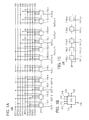
- FIG. 1A is a diagram showing an example of a shift register
- FIGS. 1B and 1C are diagrams showing examples of pulse output circuits.
- FIGS. 2A and 2B each illustrate an example of a pulse output circuit.
- FIGS. 3A and 3B each illustrate an example of a pulse output circuit.
- FIGS. 4A and 4B each illustrate an example of a pulse output circuit.
- FIGS. 5A and 5B are diagrams showing an example of a shift register and FIGS. 5C and 5D are diagrams showing examples of pulse output circuits.
- FIGS. 6A , 6 B 1 , and 6 B 2 are diagrams each showing an example of a pulse output circuit
- FIG. 6C is a diagram showing an example of a shift register.
- FIG. 7 is a timing chart illustrating operation of a shift register.
- FIG. 8 is a timing chart illustrating operation of a shift register.
- FIG. 9 is a timing chart illustrating operation of a pulse output circuit.
- FIGS. 10A and 10B are circuit diagrams illustrating operation of a pulse output circuit.
- FIGS. 11A and 11B are circuit diagrams illustrating operation of a pulse output circuit.
- FIGS. 12A and 12B are circuit diagrams illustrating operation of a pulse output circuit.
- FIGS. 13A to 13C are timing charts illustrating operation of a shift register.
- FIG. 14A is a diagram showing an example of a shift register
- FIGS. 14B and 14C are diagrams showing an example of a pulse output circuit.
- FIG. 15 is a timing chart showing operation of a shift register.
- FIG. 16 is a timing chart showing operation of a pulse output circuit.
- FIGS. 17A and 17B are circuit diagrams illustrating operation of a pulse output circuit.
- FIGS. 18A and 18B are circuit diagrams illustrating operation of a pulse output circuit.
- FIG. 19 is a circuit diagram illustrating operation of a pulse output circuit.
- FIGS. 20 A 1 , 20 A 2 , 20 B 1 , 20 B 2 , 20 C 1 , and 20 C 2 illustrate examples of transistors.
- FIGS. 21 A 1 , 21 A 2 , 21 A 3 , 21 B 1 , and 21 B 2 illustrate examples of transistors.
- FIGS. 22 A 1 , 22 A 2 , 22 A 3 , 22 B 1 , 22 B 2 , 22 C 1 , and 22 C 2 illustrate examples of transistors.
- FIGS. 23A to 23C illustrate an example of a transistor.
- FIGS. 24A to 24C illustrate an example of a transistor.
- FIGS. 25A to 25C illustrate an example of a transistor.
- FIGS. 26A and 26B illustrate an example of a transistor.
- FIGS. 27A and 27B illustrate an example of a transistor.
- FIGS. 28A to 28C illustrate an example of a transistor.
- FIGS. 29A to 29C illustrate an example of a transistor.
- FIGS. 30A to 30C illustrate an example of a transistor.
- FIGS. 31A and 31B show energy band structures.
- FIGS. 32A to 32C illustrate examples of display devices.
- FIGS. 33A and 33B illustrate examples of display devices.
- FIGS. 34A and 34B each illustrate a structure example of a driver circuit.
- FIGS. 35A to 35C each illustrate an example of a display device.
- FIGS. 36A and 36B each illustrate an example of a display device.
- FIG. 37 illustrates an example of a display module.
- FIGS. 38A to 38H illustrate examples of electronic devices.
- ordinal numbers such as “first” and “second” and the like in this specification and the like are used in order to avoid confusion among components and do not denote the priority or the order such as the order of steps or the stacking order.
- a term without an ordinal number in this specification and the like might be provided with an ordinal number in a claim in order to avoid confusion among components.
- a term with an ordinal number in this specification and the like might be provided with a different ordinal number in a claim.
- a term with an ordinal number in this specification and the like might not be provided with any ordinal number in a claim.
- an “electrode” or a “wiring” does not limit a function of a component.
- an “electrode” is used as part of a “wiring” in some cases, and vice versa.
- the term “electrode” or “wiring” can also mean a combination of a plurality of “electrodes” and “wirings” formed in an integrated manner.
- electrode B over insulating layer A does not necessarily mean that the electrode B is on and in direct contact with the insulating layer A and can mean the case where another component is provided between the insulating layer A and the electrode B.
- source and the drain might be switched depending on operation conditions, e.g., when a transistor having a different polarity is employed or a direction of current flow is changed in circuit operation.
- source and drain can be switched in this specification.
- the expression “electrically connected” includes the case where components are connected through an “object having any electric function”. There is no particular limitation on an “object having any electric function” as long as electric signals can be transmitted and received between components that are connected through the object. Accordingly, even when the expression “to be electrically connected” is used in this specification, there is a case in which no physical connection is made and a wiring is just extended in an actual circuit.
- the channel length refers to, for example, a distance between a source (source region or source electrode) and a drain (drain region or drain electrode) in a region where a semiconductor (or a portion where a current flows in a semiconductor when a transistor is on) and a gate electrode overlap with each other or a region where a channel is formed (also referred to as a “channel formation region”) in a top view of the transistor.
- channel lengths in all regions are not necessarily the same.
- the channel length of one transistor is not limited to one value in some cases. Therefore, in this specification, the channel length is any one of values, the maximum value, the minimum value, or the average value in a region where a channel is formed.
- a channel width refers to, for example, the length of a portion where a source and a drain face each other in a region where a semiconductor (or a portion where a current flows in a semiconductor when a transistor is on) and a gate electrode overlap with each other, or a region where a channel is formed in a top view.
- channel widths in all regions do not necessarily have the same value.
- a channel width of one transistor is not fixed to one value in some cases. Therefore, in this specification, a channel width is any one of values, the maximum value, the minimum value, or the average value in a region where a channel is formed.
- a channel width in a region where a channel is actually formed is different from a channel width shown in a top view of a transistor (also referred to as an “apparent channel width”) in some cases.
- an effective channel width is greater than an apparent channel width, and its influence cannot be ignored in some cases.
- the proportion of a channel region formed in a side surface of a semiconductor is increased. In that case, an effective channel width is greater than an apparent channel width.
- an effective channel width is difficult to measure in some cases. For example, to estimate an effective channel width from a design value, it is necessary to assume that the shape of a semiconductor is known as an assumption condition. Therefore, in the case where the shape of a semiconductor is not known accurately, it is difficult to measure an effective channel width accurately.
- an apparent channel width is referred to as a surrounded channel width (SCW) in some cases.
- SCW surrounded channel width
- channel width in the case where the term “channel width” is simply used, it may denote a surrounded channel width and an apparent channel width.
- channel width in the case where the term “channel width” is simply used, it may denote an effective channel width in some cases. Note that a channel length, a channel width, an effective channel width, an apparent channel width, a surrounded channel width, and the like can be determined by analyzing a cross-sectional TEM image and the like.
- a surrounded channel width may be used for the calculation. In that case, a value different from one in the case where an effective channel width is used for the calculation is obtained in some cases.
- a transistor described in this specification and the like refers to an enhancement (normally-off) field-effect transistor (FET).
- FET field-effect transistor
- a transistor described in this specification and the like is an n-channel transistor, and a source and a drain are electrically connected to each other (on state) when a voltage (V gs ) between a gate and the source exceeds the threshold voltage (V th ).
- V th of the transistors described in this specification and the like are the same.
- an impurity in a semiconductor refers to, for example, elements other than the main components of the semiconductor.
- an element with a concentration lower than 0.1 atomic % can be regarded as an impurity.
- the density of states (DOS) in a semiconductor may be increased, the carrier mobility may be decreased, or the crystallinity may be decreased.
- examples of an impurity which changes characteristics of the semiconductor include Group 1 elements, Group 2 elements, Group 13 elements, Group 14 elements, Group 15 elements, and transition metals other than the main components of the oxide semiconductor; specifically, there are hydrogen (included in water), lithium, sodium, silicon, boron, phosphorus, and carbon, for example.
- oxygen vacancy may be formed by entry of impurities such as hydrogen.
- impurities such as hydrogen.
- examples of an impurity which changes characteristics of the semiconductor include oxygen, Group 1 elements except hydrogen, Group 2 elements, Group 13 elements, and Group 15 elements.
- the term “parallel” indicates that the angle formed between two straight lines is greater than or equal to ⁇ 10° and less than or equal to 10°, and accordingly also includes the case where the angle is greater than or equal to ⁇ 5° and less than or equal to 5°.
- a term “substantially parallel” indicates that the angle formed between two straight lines is greater than or equal to ⁇ 30° and less than or equal to 30°.
- the term “perpendicular” or “orthogonal” indicates that the angle formed between two straight lines is greater than or equal to 80° and less than or equal to 100°, and accordingly also includes the case where the angle is greater than or equal to 85° and less than or equal to 95°.
- a term “substantially perpendicular” indicates that the angle formed between two straight lines is greater than or equal to 60° and less than or equal to 120°.
- a high power supply potential V DD (hereinafter also simply referred to as V DD or H potential) is a power supply potential higher than a low power supply potential V SS .
- the low power supply potential V SS (hereinafter also simply referred to as V SS or L potential) is a power supply potential lower than the high power supply potential V DD .
- a ground potential can be used as V DD or V SS .
- V SS is lower than the ground potential
- V DD is higher than the ground potential.
- a voltage usually refers to a potential difference between a given potential and a reference potential (e.g., a ground potential (GND potential) or a source potential).
- a reference potential e.g., a ground potential (GND potential) or a source potential.
- Potentials are relative values, and a potential supplied to a wiring or the like is sometimes changed depending on the reference potential.
- a voltage can be referred to as a potential and vice versa in some cases.
- V SS is referred to as a reference potential unless otherwise specified.
- film and “layer” can be interchanged with each other depending on the case or circumstances.
- conductive layer can be changed into the term “conductive film” in some cases.
- insulating film can be changed into the term “insulating layer” in some cases.
- pulse output circuits which are a kind of semiconductor circuits, and shift registers each including any of the pulse output circuits will be described with reference to drawings.
- FIGS. 14A to 14C First, an example of a configuration and operation of a conventional shift register will be described with reference to FIGS. 14A to 14C , FIG. 15 , FIG. 16 , FIGS. 17A and 17B , FIGS. 18A and 18B , and FIG. 19 .
- a shift register 900 illustrated in FIG. 14A includes n (n is a natural number of 2 or more) pulse output circuits 910 .
- n is a natural number of 2 or more pulse output circuits 910 .
- the pulse output circuit 910 in a first stage and the pulse output circuit 910 in an n-th stage are referred to as a pulse output circuit 910 _ 1 and a pulse output circuit 910 _ n , respectively, in some cases.
- the pulse output circuit 910 in an i-th stage i is a natural number of greater than or equal to 1 and less than or equal to n
- a pulse output circuit 910 _ i in some cases.
- a terminal, an output signal OUT, and the like of the pulse output circuit 910 are referred in a manner similar to the above in some cases.
- an output signal OUT of the pulse output circuit 910 _ i is referred to as an output signal OUT_i in some cases.
- the shift register 900 includes a wiring 905 through which a reset signal RES is supplied and wirings 901 to 904 through which clock signals are supplied.
- the wirings 901 to 904 are supplied with first to fourth clock signals CLK 1 to CLK 4 , respectively.
- the clock signal is a signal which changes between H and L potentials at regular intervals, and the first to fourth clock signals CLK 1 to CLK 4 are delayed by 1 ⁇ 4 period sequentially.
- control or the like of the pulse output circuit is performed with the first to fourth clock signals CLK 1 to CLK 4 .
- the pulse output circuits 910 each include terminals 911 to 916 (see FIG. 14B ).
- the terminals 911 and 912 are each electrically connected to one of the wirings 901 to 904 .
- the terminals 911 and 912 of the pulse output circuit 910 _ 1 are electrically connected to the wirings 901 and 902 , respectively.
- the terminals 911 and 912 of the pulse output circuit 910 _ 2 are electrically connected to the wirings 902 and 903 , respectively.
- the terminals 914 are electrically connected to the wiring 905 .
- a start signal SP is supplied to the terminal 913 of the pulse output circuit 910 _ 1 and an output signal OUT_ 1 is output from the terminal 916 thereof.
- the terminal 913 of the pulse output circuit 910 _ i is electrically connected to the terminal 915 of the pulse output circuit 910 _ i ⁇ 1 (pulse output circuit 910 in an i ⁇ 1-th stage).
- the terminal 915 of the pulse output circuit 910 _ i is electrically connected to the terminal 913 of the pulse output circuit 910 _ i+ 1.
- An output signal OUT_i is output from the terminal 916 of the pulse output circuit 910 _ i .
- An output signal OUT_n is output from the terminal 916 of the pulse output circuit 910 _ n in the n-th stage.
- the pulse output circuit 910 _ n does not necessarily include the terminal 915 .
- the terminal 915 may be electrically connected to the terminal 913 (terminal 913 _ 1 ) of the pulse output circuit 910 _ 1 in the first stage.
- the pulse output circuit 910 includes a transistor 921 , a transistor 922 , transistors 924 to 929 , a transistor 931 , a transistor 932 , a capacitor 933 , and a capacitor 934 .
- One of a source and a drain of the transistor 921 is electrically connected to a wiring 941 , the other of the source and the drain of the transistor 921 is electrically connected to a node 962 , and a gate of the transistor 921 is electrically connected to the terminal 912 .
- One of a source and a drain of the transistor 922 is electrically connected to the wiring 941 , the other of the source and the drain of the transistor 922 is electrically connected to the node 962 , and a gate of the transistor 922 is electrically connected to the terminal 914 .
- One of a source and a drain of the transistor 924 is electrically connected to the wiring 941 , the other of the source and the drain of the transistor 924 is electrically connected to a node 963 , and a gate of the transistor 924 is electrically connected to the terminal 913 .
- One of a source and a drain of the transistor 925 is electrically connected to the node 963 , the other of the source and the drain of the transistor 925 is electrically connected to a wiring 946 , and a gate of the transistor 925 is electrically connected to the node 962 .
- One of a source and a drain of the transistor 926 is electrically connected to the terminal 911 , the other of the source and the drain of the transistor 926 is electrically connected to the terminal 915 , and a gate of the transistor 926 is electrically connected to a node 961 .
- One of a source and a drain of the transistor 927 is electrically connected to the terminal 915 , the other of the source and the drain of the transistor 927 is electrically connected to the wiring 946 , and a gate of the transistor 927 is electrically connected to the node 962 .
- One of a source and a drain of the transistor 928 is electrically connected to the terminal 911 , the other of the source and the drain of the transistor 928 is electrically connected to the terminal 916 , and a gate of the transistor 928 is electrically connected to the node 961 .
- One of a source and a drain of the transistor 929 is electrically connected to the terminal 916 , the other of the source and the drain of the transistor 929 is electrically connected to the wiring 946 , and a gate of the transistor 929 is electrically connected to the node 962 .
- One of a source and a drain of the transistor 931 is electrically connected to the node 962 , the other of the source and the drain of the transistor 931 is electrically connected to the wiring 946 , and a gate of the transistor 931 is electrically connected to the terminal 913 .
- One of a source and a drain of the transistor 932 is electrically connected to the node 963 , the other of the source and the drain of the transistor 932 is electrically connected to the node 961 , and a gate of the transistor 932 is electrically connected to the wiring 941 .
- One electrode of the capacitor 933 is electrically connected to the node 962 , and the other electrode of the capacitor 933 is electrically connected to the wiring 946 .
- FIG. 15 is a timing chart showing the operation of the shift register 900 and shows sequential output of the output signal OUT at the H potential to the terminals 916 _ 1 to 916 _ 5 from the operation start of the shift register 900 .
- the reset signal RES is supplied to the wiring 905 (period 950 ).
- the start signal SP is supplied to the terminal 913 _ 1 of the pulse output circuit 910 _ 1 (period 951 ).
- the H potential is output from the terminals 915 _ 1 and 916 _ 1 in synchronization with the clock signal CLK 1 (period 952 ).
- the potential supplied to the terminal 915 is the same as the potential supplied to the terminal 916 ; therefore, the potential change in the terminal 915 is not shown in FIG. 15 .
- the output of the terminal 915 _ 1 is input to the terminal 913 _ 2 .
- the H potential is output from the terminal 916 _ 2 in synchronization with the clock signal CLK 2 (period 953 ).
- the output of the terminal 9152 is input to the terminal 913 _ 3 .
- the H potential is output from the terminal 916 _ 3 in synchronization with the clock signal CLK 3 .
- the output of the terminal 915 _ 3 is input to the terminal 913 _ 4 (period 954 ).
- the H potential is output from the terminal 916 _ 4 in synchronization with the clock signal CLK 4 .
- the output of the terminal 915 _ 4 is input to the terminal 913 _ 5 (period 955 ).
- the H potential is output from the terminal 916 _ 5 in synchronization with the clock signal CLK 1 .
- the output of the terminal 915 _ 5 is input to the terminal 913 _ 6 (period 956 ). In this manner, the H potential is sequentially output from the terminals 916 in the first to n-th stages.
- FIG. 16 is a timing chart showing the operation of the pulse output circuit 910 _ 1 in the first stage.
- FIGS. 17A and 17B , FIGS. 18A and 18B , and FIG. 19 are circuit diagrams showing the operation of the pulse output circuit 910 _ 1 .
- FIG. 16 shows potential changes in the terminals 911 to 916 and the nodes 961 to 963 .
- FIG. 16 further shows the on/off states of the transistor 921 , the transistor 922 , the transistors 924 to 929 , the transistor 931 , and the transistor 932 .
- the wirings 941 and 946 are supplied with the H potential and the L potential, respectively.
- Each node in the circuit is in a floating state before power is supplied to the shift register. After power is supplied to the shift register, the output signal OUT is irregularly output from the pulse output circuit 910 depending on the state of each node in some cases.
- the shift register can be normally operated by supplying the reset signal RES immediately after the power is supplied, for example.
- the reset signal RES is supplied to the terminals 914 of all of the pulse output circuits 910 .
- the transistors 922 of all of the pulse output circuits 910 are turned OD, so that the H potential (accurately, H potential ⁇ V th ) is supplied to all of the nodes 962 .
- the transistors 925 included in all of the pulse output circuits 910 are turned on, so that the L potential is supplied to all of the nodes 961 .
- all of the output signals OUT become the L potentials.
- the start signal SP is supplied to the terminal 913 , so that the transistors 924 and 931 are turned on.
- the transistor 924 When the transistor 924 is turned on, the potentials of the nodes 961 and 963 of the pulse output circuit 910 _ 1 become the H potentials (accurately, H potential ⁇ V th ), so that the transistors 926 and 928 in the pulse output circuit 910 _ 1 are turned on. Since the L potential is supplied to the terminal 911 _ 1 , the outputs of the terminals 915 _ 1 and 916 _ 1 remain at the L potentials.
- the transistor 931 When the transistor 931 is turned on, the potential of the node 962 becomes the L potential. Note that the terminals 913 _ i in the subsequent stages are supplied with the output signals of the terminals 915 _ i ⁇ 1 in the preceding stages.
- the L potential is supplied to the terminal 913 , and the H potential (clock signal CLK 1 ) is supplied to the terminal 911 .
- the transistor 924 is turned off, so that the node 961 becomes a floating state.
- the H potential is supplied to the terminal 911 , the potential of the terminal 916 is increased. Since the node 961 and the terminal 916 are connected to each other via the capacitor 934 , the potential of the node 961 is raised to 2 ⁇ VDD ⁇ V th at the maximum by the bootstrap operation. Thus, the H potential is output from the terminals 915 and 916 .
- the potential of the node 963 remains at the H potential (accurately, H potential ⁇ V th ).
- the output of the terminal 915 is input to the terminal 913 of the pulse output circuit 910 in the subsequent stage.
- a period from supply of the H potential to the terminal 913 _ i to output of the H potential from the terminal 915 _ i and/or the terminal 916 _ i is referred to as a “selection period” of the pulse output circuit 910 _ i .
- the periods 951 and 952 are collectively referred to as a selection period of the pulse output circuit 910 _ 1 .
- the periods 952 and 953 are collectively referred to as a selection period of the pulse output circuit 910 _ 2 .
- a period other than the selection period is referred to as a “non-selection period”.
- the L potential is supplied to the terminal 911 and the H potential (clock signal CLK 2 ) is supplied to the terminal 912 .
- the transistor 921 is turned on, so that the potential of the node 962 becomes the H potential (accurately, H potential ⁇ V th ).
- the transistor 925 is turned on, so that the node 961 is set at the L potential.
- the transistor 927 is turned on, so that the L potential is output from the terminal 915 .
- the transistor 929 is turned on, so that the L potential is output from the terminal 916 .
- the L potential is supplied to the terminal 912 , so that the transistor 921 is turned off.
- the L potential is output from the terminals 915 and 916 until the H potential is supplied to the terminal 913 next, even if the H potential is supplied to the terminal 911 .
- the output signal OUT at the H level can be sequentially output from the terminals 916 in the first to n-th stages.
- the potentials of the sources and the drains of the transistors 925 , 927 , 929 , and 932 are the L potentials and the potentials of the gates thereof are the H potentials until the H potential is supplied to the terminal 913 after the output signal OUT is output.
- the transistors 925 , 927 , 929 , and 932 are each set in a state where positive stress is applied to the gate during the non-selection period.
- FIGS. 1A to 1C examples of configurations and operation of a shift register of one embodiment of the present invention will be described with reference to FIGS. 1A to 1C , FIGS. 2A and 2B , FIGS. 3A and 3B , FIGS. 4A and 4B , FIGS. 5A to 5D , FIGS. 6A to 6C , FIG. 7 , and FIG. 8 .
- a shift register 100 illustrated in FIG. 1A includes n pulse output circuits 110 .
- the pulse output circuit 110 in a first stage and the pulse output circuit 110 in an n-th stage are referred to as a pulse output circuit 110 _ 1 and a pulse output circuit 110 _ n , respectively, in some cases.
- the pulse output circuit 110 in an i-th stage is referred to as a pulse output circuit 110 _ i in some cases.
- a terminal, an output signal OUT, and the like of the pulse output circuit 110 are referred in a manner similar to the above in some cases.
- an output signal OUT of the pulse output circuit 110 _ i is referred to as an output signal OUT_i in some cases.
- the shift register 100 includes wirings 101 to 104 through which clock signals are supplied, a wiring 105 through which the reset signal RES is supplied, a wiring 106 through which a signal DTY 1 is supplied, a wiring 107 through which a signal DTY 2 is supplied, a wiring 108 through which a signal DTY 3 is supplied, and a wiring 109 through which a signal DTY 4 is supplied.
- the wirings 101 to 104 are supplied with the first to fourth clock signals CLK 1 to CLK 4 , respectively.
- the pulse output circuits 110 each include terminals 111 to 118 (see FIG. 1B ).
- the terminals 111 and 112 are each electrically connected to one of the wirings 101 to 104 .
- the terminals 111 and 112 of the pulse output circuit 110 _ 1 in the first stage are electrically connected to the wirings 101 and 102 , respectively.
- the terminals 111 and 112 of the pulse output circuit 110 _ 2 in the second stage are electrically connected to the wirings 102 and 103 , respectively.
- the terminals 114 are electrically connected to the wiring 105 .
- the start signal SP is supplied to the terminal 113 of the pulse output circuit 110 _ 1 in the first stage and the output signal OUT_ 1 is output from the terminal 116 thereof.
- the terminal 113 of the pulse output circuit 110 _ i in the i-th stage is electrically connected to the terminal 115 of the pulse output circuit 110 _ i ⁇ 1 in an i ⁇ 1-th stage.
- the terminal 115 of the pulse output circuit 110 _ i in the i-th stage is electrically connected to the terminal 113 of the pulse output circuit 110 _ i +1 in an i+l-th stage.
- the output signal OUT_i is output from the terminal 116 of the pulse output circuit 110 _ i in the i-th stage.
- the output signal OUT_n is output from the terminal 116 of the pulse output circuit 110 _ n in the n-th stage.
- the pulse output circuit 110 _ n in the n-th stage does not necessarily include the terminal 115 .
- the terminal 115 may be electrically connected to the terminal 113 _ 1 of the pulse output circuit 110 _ 1 in the first stage (see FIG. 1C ).
- the terminals 117 and 118 are electrically connected to the wirings 106 and 107 , respectively.
- the terminals 117 and 118 are electrically connected to the wirings 108 and 109 , respectively.
- the pulse output circuit 110 includes a transistor 121 , a transistor 122 , transistors 124 to 129 , a transistor 131 , a transistor 132 , a transistor 135 , a transistor 136 , and a capacitor 134 .
- a transistor including a gate and a back gate is used as each of the transistors 125 , 127 , 129 , and 132 .
- the back gate is formed using a conductive layer.
- the gate and the back gate are positioned so that a channel formation region of a semiconductor layer is provided between the gate and the back gate.
- the back gate can function in a manner similar to that of the gate.
- the potential of the back gate may be the same as that of the gate or may be a GND potential or a given potential.
- the threshold voltage of the transistor can be changed.
- one of the gate and the back gate is referred to as a “first gate”, and the other is referred to as a “second gate”.
- One of a source and a drain of the transistor 121 is electrically connected to a wiring 141 , the other of the source and the drain of the transistor 121 is electrically connected to a node 164 , and a gate of the transistor 121 is electrically connected to the terminal 112 .
- One of a source and a drain of the transistor 122 is electrically connected to the wiring 141 , the other of the source and the drain of the transistor 122 is electrically connected to the node 164 , and a gate of the transistor 122 is electrically connected to the terminal 114 .
- One of a source and a drain of the transistor 124 is electrically connected to the wiring 141 , the other of the source and the drain of the transistor 124 is electrically connected to a node 163 , and a gate of the transistor 124 is electrically connected to the terminal 113 .
- One of a source and a drain of the transistor 125 is electrically connected to the node 163 , the other of the source and the drain of the transistor 125 is electrically connected to a wiring 145 , a first gate of the transistor 125 is electrically connected to the node 162 , and a second gate of the transistor 125 is electrically connected to the terminal 117 .
- One of a source and a drain of the transistor 126 is electrically connected to the terminal 111 , the other of the source and the drain of the transistor 126 is electrically connected to the terminal 115 , and a gate of the transistor 126 is electrically connected to a node 161 .
- One of a source and a drain of the transistor 127 is electrically connected to the terminal 115 , the other of the source and the drain of the transistor 127 is electrically connected to the wiring 145 , a first gate of the transistor 127 is electrically connected to the node 162 , and a second gate of the transistor 127 is electrically connected to the terminal 117 .
- One of a source and a drain of the transistor 128 is electrically connected to the terminal 111 , the other of the source and the drain of the transistor 128 is electrically connected to the terminal 116 , and a gate of the transistor 128 is electrically connected to the node 161 .
- One of a source and a drain of the transistor 129 is electrically connected to the terminal 116 , the other of the source and the drain of the transistor 129 is electrically connected to the wiring 145 , a first gate of the transistor 129 is electrically connected to the node 162 , and a second gate of the transistor 129 is electrically connected to the terminal 117 .
- One of a source and a drain of the transistor 131 is electrically connected to the node 164 , the other of the source and the drain of the transistor 131 is electrically connected to the wiring 145 , and a gate of the transistor 131 is electrically connected to the terminal 113 .
- One of a source and a drain of the transistor 132 is electrically connected to the node 163 , the other of the source and the drain of the transistor 132 is electrically connected to the node 161 , a first gate of the transistor 132 is electrically connected to the terminal 118 , and a second gate of the transistor 132 is electrically connected to the terminal 117 .
- One of a source and a drain of the transistor 135 is electrically connected to the node 164 , the other of the source and the drain of the transistor 135 is electrically connected to the node 162 , and a gate of the transistor 135 is electrically connected to the terminal 118 .
- One of a source and a drain of the transistor 136 is electrically connected to the node 162 , the other of the source and the drain of the transistor 136 is electrically connected to the wiring 145 , and a gate of the transistor 136 is electrically connected to the terminal 117 .
- One electrode of the capacitor 134 is electrically connected to the node 161 , and the other electrode of the capacitor 134 is electrically connected to the terminal 116 .
- the pulse output circuit 110 of one embodiment of the present invention can be formed using transistors having the same conductivity type. Thus, a pulse output circuit can be provided with high productivity. A semiconductor device can be provided with high productivity. Although the pulse output circuit 110 is formed using n-channel transistors in this embodiment, they can be replaced with p-channel transistors.
- one of the source and the drain of the transistor 121 may be electrically connected to a wiring 142 and one of the source and the drain of the transistor 124 may be electrically connected to a wiring 143 .
- the other of the source and the drain of the transistor 125 may be electrically connected to a wiring 146
- the other of the source and the drain of the transistor 136 may be electrically connected to a wiring 147
- the other of the source and the drain of the transistor 127 may be electrically connected to a wiring 148
- the other of the source and the drain of the transistor 129 may be electrically connected to a wiring 149 .
- the wirings 141 to 143 may be supplied with the same potential or different potentials.
- the wirings 145 to 149 may be supplied with the same potential or different potentials.
- the capacitor 134 is not necessarily provided as in a pulse output circuit 110 b in the circuit diagram of FIG. 3A .
- the capacitor 134 When the capacitor 134 is not provided, the area occupied by the pulse output circuit can be reduced. Thus, the degree of integration of the pulse output circuit of one embodiment of the present invention can be increased. Accordingly, the degree of integration of the semiconductor device of one embodiment of the present invention can be increased. The productivity of pulse output circuits of one embodiment of the present invention can be increased. Accordingly, the productivity of semiconductor devices of one embodiment of the present invention can be increased.
- a capacitor 137 may be provided between the node 164 and the wiring 145 . Specifically, one electrode of the capacitor 137 is electrically connected to the node 164 , and the other electrode of the capacitor 137 is electrically connected to the wiring 145 . Note that the other electrode of the capacitor 137 may be connected to a predetermined wiring through which a predetermined potential is supplied.
- a pulse output circuit of one embodiment of the present invention can be operated stably.
- a semiconductor device of one embodiment of the present invention can be operated stably.
- a capacitor 138 may be provided between the node 162 and the wiring 145 . Specifically, one electrode of the capacitor 138 is electrically connected to the node 162 and the other electrode of the capacitor 138 is electrically connected to the wiring 145 . Note that the other electrode of the capacitor 138 may be connected to a predetermined wiring through which a predetermined potential is supplied.
- a pulse output circuit of one embodiment of the present invention can be operated stably.
- a semiconductor device of one embodiment of the present invention can be operated stably.
- a transistor including a back gate may be used as each of the transistors 121 , 122 , 124 , 126 , 128 , 131 , 135 , and 136 .
- a first gate and a second gate of each of the transistors 121 , 122 , 124 , 126 , 128 , and 135 are electrically connected to each other. Furthermore, one of a first gate and a second gate of the transistor 131 is electrically connected to the terminal 113 , and the other of the first gate and the second gate of the transistor 131 is electrically connected to the wiring 145 . Note that the first gate and the second gate may be electrically connected to each other instead of connecting the other of the first gate and the second gate of the transistor 131 to the wiring 145 .
- one of a first gate and a second gate of the transistor 136 is electrically connected to the terminal 117 and the other of the first gate and the second gate of the transistor 136 is electrically connected to the wiring 145 .
- the other of the first gate and the second gate of the transistor 136 is not necessarily connected to the wiring 145 , and the first gate and the second gate may be electrically connected to each other.
- the use of a transistor including a back gate enables the area occupied by the pulse output circuit to be reduced; thus, the degree of integration of the pulse output circuit of one embodiment of the present invention can be increased. Accordingly, the degree of integration of the semiconductor device of one embodiment of the present invention can be increased.
- the productivity of pulse output circuits of one embodiment of the present invention can be increased. Accordingly, the productivity of semiconductor devices of one embodiment of the present invention can be increased.
- the reliability of the pulse output circuit can be increased. Thus, the reliability of the semiconductor device of one embodiment of the present invention can be increased.
- FIG. 5B is a block diagram of the pulse output circuit 110 f .
- FIG. 5C is a block diagram of the shift register 100 f including the pulse output circuit 110 f .
- the terminal 116 (terminal 116 _ n ) in the n-th stage may be electrically connected to the terminal 113 (terminal 113 _ 1 ) in the first stage.
- the pulse output circuit 110 f does not include the terminal 115 , in the shift register 100 f , the potential output to the terminal 116 of the pulse output circuit 110 f in the i ⁇ 1-th stage is input to the terminal 113 of the pulse output circuit 110 f in the i-th stage.
- the potential output to the terminal 116 of the pulse output circuit 110 f in the i-th stage is input to the terminal 113 of the pulse output circuit 110 f in the i+l-th stage.
- the area occupied by the pulse output circuit can be reduced; thus, the degree of integration of the pulse output circuit of one embodiment of the present invention can be increased.
- the productivity of pulse output circuits of one embodiment of the present invention can be increased. Accordingly, the degree of integration of the semiconductor device of one embodiment of the present invention can be increased. The productivity of semiconductor devices of one embodiment of the present invention can be increased.
- a transistor 123 and a terminal 119 may be provided in the pulse output circuit 110 .
- one of a source and a drain of the transistor 123 is electrically connected to the wiring 141
- the other of the source and the drain of the transistor 123 is electrically connected to the node 164
- a gate of the transistor 123 is electrically connected to the terminal 119 .
- FIG. 6 B 1 is a block diagram of the pulse output circuit 110 g .
- FIG. 6C is a block diagram of the shift register 100 g including the pulse output circuit 110 g.
- the terminal 115 of the pulse output circuit 110 g in an i-th stage is electrically connected to the terminal 119 of the pulse output circuit 110 g in an i ⁇ 1-th stage.
- the terminal 115 of the pulse output circuit 110 g in the n-th stage is electrically connected to the terminal 119 of the pulse output circuit 110 g in the n ⁇ 1-th stage.
- FIG. 6 B 2 is a block diagram of the pulse output circuit 110 g _D.
- the pulse output circuit 110 g _D is a dummy circuit for supplying a signal to the terminal 119 _ n . Therefore, the pulse output circuit 110 g _D does not necessarily include the terminal 116 and the terminal 119 .
- the semiconductor device of one embodiment of the present invention can be operated at high speed.
- the reliability of the semiconductor device of one embodiment of the present invention can be increased.
- FIG. 7 and FIG. 8 are timing charts showing the operation of the shift register 100 and show sequential output of the output signal OUT at the H potential to the terminals 116 _ 1 to 116 _ 4 from the operation start of the shift register 100 .
- the reset signal RES is supplied to the wiring 105 (period 150 ).
- the start signal SP is supplied to the terminal 113 _ 1 of the pulse output circuit 110 _ 1 (period 151 ).
- the H potential is output from the terminals 115 _ 1 and 116 _ 1 in synchronization with the clock signal CLK 1 (period 152 ).
- the potential output from the terminal 115 is the same as the potential output from the terminal 116 ; therefore, the potential change in the terminal 115 is not shown in FIG. 7 .
- the output of the terminal 115 _ 1 is input to the terminal 113 _ 2 .
- the H potential is output from the terminal 116 _ 2 in synchronization with the clock signal CLK 2 (period 153 ).
- the output of the terminal 115 _ 2 is input to the terminal 113 _ 3 .
- the H potential is output from the terminal 116 _ 3 in synchronization with the clock signal CLK 3 .
- the output of the terminal 115 _ 3 is input to the terminal 113 _ 4 (period 154 ).
- the H potential is output from the terminal 116 _ 4 in synchronization with the clock signal CLK 4 .
- the output of the terminal 115 _ 4 is input to the terminal 113 _ 5 (period 155 ).
- the H potential is output from the terminal 116 _ 5 in synchronization with the clock signal CLK 1 .
- the output of the terminal 115 _ 5 is input to the terminal 113 _ 6 (period 156 ). In this manner, the H potential is sequentially output from the terminals 116 in the first to n-th stages.
- a period from the input of the start signal SP to the next input of the start signal SP is referred to as a frame period 171 .
- the output of the terminal 115 _ n or the terminal 116 _ n serves as the start signal SP, and the above operation can be repeated.
- a period 191 the H potential is output from the terminal 116 _ k ⁇ 1, the signal DTY 3 becomes the L potential, and the signal DTY 4 becomes the H potential.
- a period 192 the H potential is output from the terminal 116 _ k .
- the H potential is output from the terminal 116 _ k +1, the signal DTY 1 becomes the H potential, and the signal DTY 2 becomes the L potential.
- the periods 191 to 193 are collectively referred to as a switching period 172 b .
- the periods 151 to 153 and the periods 251 to 253 are collectively referred to as switching periods 172 a.
- the start signal SP (H potential) is input to the terminal 113 _ 1 , and the second frame period 171 is started.
- the start signal SP is supplied to the terminal 113 _ 1 , the H potential is output from the terminal 116 _ n , the signal DTY 1 becomes the L potential, and the signal DTY 2 becomes the H potential.
- the H potential is output from the terminal 116 _ 1 .
- the H potential is output from the terminal 1162 , the signal DTY 3 becomes the H potential, and the signal DTY 4 becomes the L potential.
- a k ⁇ 1-th stage means an n-th stage
- a k+1-th stage means a first stage.
- the periods 251 to 253 correspond to the periods 151 to 153 . That is, the periods 251 to 253 are also a switching period. Similarly, the periods 151 to 153 are also a switching period.
- the periods 251 to 253 and the periods 151 to 153 are collectively referred to as switching periods 172 a.
- Pulse Output Circuit 110 Pulse Output Circuit 910 _ 1 ]
- FIG. 9 is a timing chart showing the operation of the pulse output circuit 110 _ 1 in the first stage.
- FIGS. 10A and 10B , FIGS. 11A and 11B , and FIGS. 12A and 12B are circuit diagrams showing the operation of the pulse output circuit 110 _ 1 .
- FIG. 9 shows potential changes in the terminals 111 to 116 and the nodes 161 to 163 .
- FIG. 9 further shows the on/off states of the transistor 121 , the transistor 122 , the transistors 124 to 129 , the transistor 131 , the transistor 132 , and the transistor 135 .
- the wirings 141 and 145 are supplied with the H potential and the L potential, respectively.
- the reset signal RES is supplied to the terminals 114 of all of the pulse output circuits 110 through the wiring 105 .
- the signals DTY 1 and DTY 3 are the L potentials and the signals DTY 2 and DTY 4 are the H potentials.
- the terminals 117 of all of the pulse output circuits 110 are supplied with the L potential, and the terminals 118 thereof are supplied with the H potential.
- the transistors 122 and the transistors 135 of all of the pulse output circuits 110 are turned on, and the H potential (accurately, H potential ⁇ V th ) is supplied to all of the nodes 162 .
- the transistors 125 in all of the pulse output circuits 110 are turned on, and the L potential is supplied to all of the nodes 161 .
- all of the output signals OUT become the L potentials.
- the transistors 122 of all of the pulse output circuits 110 are turned off.
- the start signal SP is supplied to the terminal 113 _ 1 , the transistors 124 and 131 are turned on.
- the transistor 124 is turned on, the potentials of the nodes 161 and 163 become the H potentials (accurately, H potential ⁇ V th ), so that the transistors 126 and 128 are turned on. Since the L potential is supplied to the terminal 111 , the outputs of the terminals 115 and 116 remain at the L potentials.
- the transistor 131 is turned on, the potential of the node 162 becomes the L potential. Note that the terminals 113 _ i in the subsequent stages are supplied with the output signals of the terminals 115 _ i ⁇ 1 in the preceding stages.
- the L potential is supplied to the terminal 113 , and the H potential (clock signal CLK 1 ) is supplied to the terminal 111 .
- the transistor 124 is turned off, so that the nodes 161 and 163 each become a floating state.
- the H potential is supplied to the terminal 111 , the potentials of the terminals 115 _ 1 and 116 _ 1 are increased.
- the potential of the node 161 is raised to 2 ⁇ VDD ⁇ V th at the maximum by the bootstrap operation.
- the H potential is output from the terminals 115 and 116 .
- the node 163 is electrically connected to the node 161 via the transistor 132 , the potential of the node 163 remains at the H potential (accurately, H potential ⁇ V th ).
- the output of the terminal 115 is input to the terminal 113 _ 2 of the pulse output circuit 110 _ 2 in the subsequent stage.
- a period from supply of the H potential to the terminal 113 _ i to output of the H potential from the terminal 115 _ i and/or the terminal 116 _ i is referred to as a selection period of the pulse output circuit 110 _ i .
- the periods 151 and 152 are collectively referred to as a selection period of the pulse output circuit 110 _ 1 .
- a period other than the periods 151 and 152 is referred to as a non-selection period of the pulse output circuit 110 _ 1 .
- the L potential is supplied to the terminal 111 _ 1 and the H potential (clock signal CLK 2 ) is supplied to the terminal 112 _ 1 .
- the transistor 121 is turned on, so that the potential of the node 162 becomes the H potential (accurately, H potential ⁇ V th ).
- the transistor 125 is turned on, the nodes 161 and 163 are each set at the L potential.
- the transistor 127 is turned on, so that the L potential is output from the terminal 115 _ 1 .
- the transistor 129 is turned on, so that the L potential is output from the terminal 116 _ 1 .
- the signal DTY 3 becomes the H potential and the signal DTY 4 becomes the L potential.
- the L potential is supplied to the terminal 112 _ 1 , so that the transistor 121 is turned off.
- the L potential is output from the terminals 115 _ 1 and 116 _ 1 until the H potential is supplied to the terminal 113 _ 1 next, even if the H potential is supplied to the terminal 111 .
- the output signal OUT at the H level can be sequentially output from the terminals 116 in the first to n-th stages.
- the signals DTY 1 and DTY 4 are the L potentials and the signals DTY 2 and DTY 3 are the H potentials until the switching period 172 b .
- the H potential is supplied to the first gate of each of the transistors 125 , 127 , 129 , and 132 , and the L potential is supplied to the second gate of each of them (see FIG. 12A ).
- the signals DTY 1 and DTY 4 are the H potentials
- the signals DTY 2 and DTY 3 are the L potentials.
- the L potential is supplied to the first gate of each of the transistors 125 , 127 , 129 , and 132
- the H potential is supplied to the second gate of each of them (see FIG. 12B ).
- FIGS. 13A to 13C are timing charts of the start signal SP and the signals DTY 1 to DTY 4 .
- the case where two switching periods 172 (switching periods 172 a and 172 b ) are provided per frame period 171 is described (see FIG. 13A ).
- one embodiment of the present invention is not limited thereto, and two or more switching periods 172 may be provided per frame period 171 .
- four switching periods 172 switching periods 172 a to 172 d
- the duty cycles of the signals DTY 1 to DTY 4 can be determined arbitrarily (see FIG. 13C ).
- the duty cycles of the signals DTY 1 to DTY 4 are preferably 30% to 70%, further preferably 40% to 60%, still further preferably 45% to 55%.
- the duty cycle refers to the percentage of a period of the H potential to one frame period of a specific signal.
- This embodiment can be implemented in appropriate combination with any of the structures described in the other embodiments and the like.
- the pulse output circuit of one embodiment of the present invention can be fabricated by using a transistor with any of various structures, such as a bottom-gate transistor or a top-gate transistor. Therefore, a material for a semiconductor layer or the structure of a transistor can be easily changed depending on the existing production line.
- FIG. 20 A 1 is a cross-sectional view of a channel-protective transistor 410 that is a type of bottom-gate transistor.
- the transistor 410 includes an electrode 246 over a substrate 271 with an insulating layer 272 positioned therebetween.
- the transistor 410 includes a semiconductor layer 242 over the electrode 246 with an insulating layer 226 provided therebetween.
- the electrode 246 can function as a gate electrode.
- the insulating layer 226 can function as a gate insulating layer.
- the transistor 410 includes an insulating layer 225 over a channel formation region in the semiconductor layer 242 .
- the transistor 410 includes an electrode 244 a and an electrode 244 b which are partly in contact with the semiconductor layer 242 and over the insulating layer 226 . Part of the electrode 244 a and part of the electrode 244 b are formed over the insulating layer 225 .
- the insulating layer 225 can function as a channel protective layer. With the insulating layer 225 provided over the channel formation region, the semiconductor layer 242 can be prevented from being exposed at the time of forming the electrodes 244 a and 244 b . Thus, the channel formation region in the semiconductor layer 242 can be prevented from being etched at the time of forming the electrodes 244 a and 244 b . According to one embodiment of the present invention, a transistor with favorable electrical characteristics can be provided.
- the transistor 410 includes an insulating layer 228 over the electrode 244 a , the electrode 244 b , and the insulating layer 225 and further includes an insulating layer 229 over the insulating layer 228 .
- a material that is capable of removing oxygen from part of the semiconductor layer 242 to generate oxygen vacancies is preferably used at least for regions of the electrodes 244 a and 244 b that are in contact with the semiconductor layer 242 .
- the carrier concentration of the regions of the semiconductor layer 242 in which oxygen vacancies are generated is increased, so that the regions become n-type regions (n + layers). Accordingly, the regions can function as a source region and a drain region.
- Examples of the material which is capable of removing oxygen from the oxide semiconductor to generate oxygen vacancies include tungsten and titanium.
- Formation of the source region and the drain region in the semiconductor layer 242 makes it possible to reduce contact resistance between the semiconductor layer 242 and each of the electrodes 244 a and 244 b . Accordingly, the electrical characteristics of the transistor, such as the field-effect mobility and the threshold voltage, can be favorable.
- a layer that functions as an n-type semiconductor or a p-type semiconductor is preferably provided between the semiconductor layer 242 and the electrode 244 a and between the semiconductor layer 242 and the electrode 244 b .
- the layer that functions as an n-type semiconductor or a p-type semiconductor can function as a source region or a drain region in a transistor.
- the insulating layer 229 is preferably formed using a material that can prevent or reduce diffusion of impurities into the transistor from the outside. The formation of the insulating layer 229 may also be omitted.
- heat treatment may be performed before and/or after the insulating layer 229 is formed.
- the heat treatment can fill oxygen vacancies in the semiconductor layer 242 by diffusing oxygen contained in the insulating layer 229 or other insulating layers into the semiconductor layer 242 .
- the insulating layer 229 may be formed while the heat treatment is performed, so that oxygen vacancies in the semiconductor layer 242 can be filled.
- a transistor 411 illustrated in FIG. 20 A 2 is different from the transistor 410 in that an electrode 223 that can function as a back gate is provided over the insulating layer 229 .
- the electrode 223 can be formed using a material and a method similar to those of the electrode 246 .
- a back gate is formed using a conductive layer and positioned so that the channel formation region of the semiconductor layer is located between the gate and the back gate.
- the back gate can function in a manner similar to that of the gate.
- the potential of the back gate may be the same as that of the gate electrode or may be a GND potential or a predetermined potential.
- the electrode 246 and the electrode 223 can each function as a gate.
- the insulating layers 226 , 228 , and 229 can each function as a gate insulating layer.
- the electrode 223 may also be provided between the insulating layers 228 and 229 .
- one of the electrode 246 and the electrode 223 is simply referred to as a “gate” or a “gate electrode”, the other can be referred to as a “back gate” or a “back gate electrode”.
- the transistor 411 in the case where the electrode 223 is referred to as a “gate electrode”, the electrode 246 is referred to as a “back gate electrode”.
- the transistor 411 can be regarded as a kind of top-gate transistor.
- one of the electrode 246 and the electrode 223 may be referred to as a “first gate” or a “first gate electrode”, and the other may be referred to as a “second gate” or a “second gate electrode”.
- the electrode 246 and the electrode 223 With the electrode 246 and the electrode 223 with the semiconductor layer 242 provided therebetween and setting the potentials of the electrode 246 and the electrode 223 to be the same, a region of the semiconductor layer 242 through which carriers flow is enlarged in the film thickness direction; thus, the number of transferred carriers is increased. As a result, the on-state current and the field-effect mobility of the transistor 411 are increased.
- the transistor 411 has large on-state current for the area occupied thereby. That is, the area occupied by the transistor 411 can be small for required on-state current. With one embodiment of the present invention, the area occupied by a transistor can be reduced. Therefore, a semiconductor device having a high degree of integration can be provided.
- the gate and the back gate are formed using conductive layers and thus each have a function of preventing an electric field generated outside the transistor from influencing the semiconductor layer in which the channel is formed (in particular, an electric field blocking function against static electricity and the like).
- an electric field blocking function against static electricity and the like against static electricity and the like.
- the electrode 246 (gate) and the electrode 223 (back gate) each have a function of blocking an electric field from the outside, electric charge of charged particles and the like generated on the insulating layer 272 side or above the electrode 223 do not influence the channel formation region in the semiconductor layer 242 .
- a stress test e.g., a negative gate bias temperature ( ⁇ GBT) stress test in which negative charges are applied to a gate
- ⁇ GBT negative gate bias temperature
- a change in gate voltage (rising voltage) at which on-state current starts flowing at different drain voltages can be reduced. Note that this effect is obtained when the electrodes 246 and 223 have the same potential or different potentials.
- the GBT stress test is one kind of acceleration test and can evaluate, in a short time, a change by long-term use (i.e., a change over time) in characteristics of a transistor.
- the amount of change in threshold voltage of the transistor between before and after the GBT stress test is an important indicator when examining the reliability of the transistor. As the change in the threshold voltage is smaller, the transistor has higher reliability.
- the amount of change in threshold voltage is reduced. Accordingly, a variation in electrical characteristics among a plurality of transistors is also reduced.
- the transistor including the back gate has a smaller change in threshold voltage by a positive GBT stress test in which positive electric charge is applied to a gate than a transistor including no back gate.
- the back gate When the back gate is formed using a light-blocking conductive film, light can be prevented from entering the semiconductor layer from the back gate side. Therefore, photodegradation of the semiconductor layer can be prevented and deterioration in electrical characteristics of the transistor, such as a shift of the threshold voltage, can be prevented.
- a transistor with high reliability can be provided.
- a pulse output circuit, a semiconductor device, or the like with high reliability can be provided.
- FIG. 20 B 1 is a cross-sectional view of a channel-protective transistor 420 that is a type of bottom-gate transistor.
- the transistor 420 has substantially the same structure as the transistor 410 but is different from the transistor 410 in that the insulating layer 225 having openings 231 a and 231 b covers the semiconductor layer 242 .
- the openings 231 a and 231 b are formed by selectively removing part of the insulating layer 225 which overlaps with the semiconductor layer 242 .
- the semiconductor layer 242 is electrically connected to the electrode 244 a in the opening 231 a .
- the semiconductor layer 242 is electrically connected to the electrode 244 b in the opening 231 b .
- the semiconductor layer 242 can be prevented from being exposed at the time of forming the electrodes 244 a and 244 b .
- the semiconductor layer 242 can be prevented from being reduced in thickness at the time of forming the electrodes 244 a and 244 b .
- a region of the insulating layer 225 which overlaps with the channel formation region can function as a channel protective layer.
- a transistor 421 illustrated in FIG. 20 B 2 is different from the transistor 420 in that the electrode 223 that can function as a back gate is provided over the insulating layer 229 .
- the distance between the electrodes 244 a and 246 and the distance between the electrodes 244 b and 246 in the transistors 420 and 421 are longer than those in the transistors 410 and 411 .
- the parasitic capacitance generated between the electrodes 244 a and 246 can be reduced.
- the parasitic capacitance generated between the electrodes 244 b and 246 can be reduced.
- a transistor with favorable electrical characteristics can be provided.
- a transistor 425 illustrated in FIG. 20 C 1 is a channel-etched transistor that is a type of bottom-gate transistor.
- the insulating layer 225 is not provided and the electrodes 244 a and 244 b are formed to be in contact with the semiconductor layer 242 .
- part of the semiconductor layer 242 that is exposed when the electrodes 244 a and 244 b are formed is etched in some cases.
- the productivity of the transistor can be increased.
- a transistor 426 illustrated in FIG. 20 C 2 is different from the transistor 425 in that the electrode 223 which can function as a back gate is provided over the insulating layer 229 .
- FIG. 21 A 1 is a cross-sectional view of a transistor 430 that is a type of top-gate transistor.
- the transistor 430 includes the semiconductor layer 242 over the substrate 271 with the insulating layer 272 therebetween, the electrodes 244 a and 244 b that are over the semiconductor layer 242 and the insulating layer 272 and in contact with part of the semiconductor layer 242 , the insulating layer 226 over the semiconductor layer 242 and the electrodes 244 a and 244 b , and the electrode 246 over the insulating layer 226 .
- the electrode 246 overlaps with neither the electrode 244 a nor the electrode 244 b in the transistor 430 , the parasitic capacitance generated between the electrodes 246 and 244 a and the parasitic capacitance generated between the electrodes 246 and 244 b can be reduced.
- an impurity 255 is introduced into the semiconductor layer 242 using the electrode 246 as a mask, so that an impurity region can be formed in the semiconductor layer 242 in a self-aligned manner (see FIG. 21 A 3 ).
- a transistor with favorable electrical characteristics can be provided.
- the introduction of the impurity 255 can be performed with an ion implantation apparatus, an ion doping apparatus, or a plasma treatment apparatus.
- the impurity 255 for example, at least one element of a Group 13 element, a Group 15 element, and the like can be used.
- an oxide semiconductor is used for the semiconductor layer 242 , it is possible to use at least one kind of element of a rare gas and hydrogen as the impurity 255 .
- a transistor 431 illustrated in FIG. 21 A 2 is different from the transistor 430 in that the electrode 223 and the insulating layer 227 are included.
- the transistor 431 includes the electrode 223 formed over the insulating layer 272 and the insulating layer 227 formed over the electrode 223 .
- the electrode 223 can function as a back gate.
- the insulating layer 227 can function as a gate insulating layer.
- the insulating layer 227 can be formed using a material and a method similar to those of the insulating layer 226 .
- the transistor 431 as well as the transistor 411 has large on-state current for the area occupied thereby. That is, the area occupied by the transistor 431 can be small for required on-state current. With one embodiment of the present invention, the area occupied by a transistor can be reduced. Therefore, with one embodiment of the present invention, a semiconductor device having a high degree of integration can be provided.
- a transistor 440 shown in FIG. 21 B 1 as an example is a type of top-gate transistor.
- the transistor 440 is different from the transistor 430 in that the semiconductor layer 242 is formed after the formation of the electrodes 244 a and 244 b .
- a transistor 441 illustrated in FIG. 21 B 2 is different from the transistor 440 in that the electrode 223 and the insulating layer 227 are included.
- part of the semiconductor layer 242 is formed over the electrode 244 a and another part of the semiconductor layer 242 is formed over the electrode 244 b.
- the transistor 441 as well as the transistor 411 has a high on-state current for its area. That is, the area occupied by the transistor 441 can be small for required on-state current. With one embodiment of the present invention, the area occupied by a transistor can be reduced. Therefore, a semiconductor device having a high degree of integration can be provided.
- a transistor 442 illustrated in FIG. 22 A 1 as an example is a type of top-gate transistor.
- the transistor 442 has the electrodes 244 a and 244 b over the insulating layer 229 .
- the electrodes 244 a and 244 b are electrically connected to the semiconductor layer 242 through openings formed in the insulating layers 228 and 229 .
- the insulating layer 226 included in the transistor 442 is partly extended across the ends of the electrode 246 .
- the impurity 255 is added to the semiconductor layer 242 using the electrode 246 and the insulating layer 226 as masks, so that an impurity region can be formed in the semiconductor layer 242 in a self-aligned manner (see FIG. 22 A 3 ).
- the impurity 255 is not added to the semiconductor layer 242 in a region overlapping with the electrode 246 , and the impurity 255 is added to the semiconductor layer 242 in a region that does not overlap with the electrode 246 .
- the semiconductor layer 242 in a region into which the impurity 255 is introduced through the insulating layer 226 has a lower impurity concentration than the semiconductor layer 242 in a region into which the impurity 255 is introduced without through the insulating layer 226 .
- a lightly doped drain (LDD) region is formed in the semiconductor layer 242 in a region adjacent to the electrode 246 when seen from the above.
- a transistor 443 illustrated in FIG. 22 A 2 is different from the transistor 442 in that the transistor 443 includes the electrode 223 under the semiconductor layer 242 .
- the electrode 223 and the semiconductor layer 242 overlap with each other with the insulating layer 272 positioned therebetween.
- the electrode 223 can function as a back gate electrode.
- the insulating layer 226 in a region that does not overlap with the electrode 246 may be wholly removed.
- the insulating layer 226 except for the openings may be left without being removed.
- the impurity 255 is added to the semiconductor layer 242 using the electrode 246 as a mask, so that an impurity region can be formed in the semiconductor layer 242 in a self-aligned manner.
- FIGS. 23A to 23C illustrate an example of a structure of a transistor including an oxide semiconductor for the semiconductor layer 242 .
- FIG. 23A is a top view of a transistor 451 .
- FIG. 23B is a cross-sectional view (in the channel length direction) of a portion along the dashed-dotted line L 1 -L 2 in FIG. 23A .
- FIG. 23C is a cross-sectional view (in the channel width direction) of a portion along the dash-dotted line W 1 -W 2 in FIG. 23A .
- the transistor 451 includes the semiconductor layer 242 , the insulating layer 226 , the insulating layer 272 , an insulating layer 282 , an insulating layer 274 , an electrode 224 , an electrode 243 , the electrode 244 a , and the electrode 244 b .
- the electrode 243 can function as a gate
- the electrode 224 can function as a back gate.
- the insulating layer 226 , the insulating layer 272 , the insulating layer 282 , and the insulating layer 274 each can function as a gate insulating layer.
- the electrode 244 a can function as one of a source electrode and a drain electrode.
- the electrode 244 b can function as the other of the source electrode and the drain electrode.
- An insulating layer 275 is provided over the substrate 271 , and the electrode 224 and an insulating layer 273 are provided over the insulating layer 275 .
- the insulating layer 274 is provided over the electrode 224 and the insulating layer 273 .
- the insulating layer 282 is provided, and over the insulating layer 282 , the insulating layer 272 is provided.
- a semiconductor layer 242 a is provided over a projection formed in the insulating layer 272
- a semiconductor layer 242 b is provided over the semiconductor layer 242 a .
- the electrode 244 a and the electrode 244 b are provided over the semiconductor layer 242 b .
- a region in the semiconductor layer 242 b which overlaps with the electrode 244 a can function as one of a source and a drain of the transistor 451 .
- a region in the semiconductor layer 242 b which overlaps with the electrode 244 b can function as the other of the source and the drain of the transistor 451 .
- a semiconductor layer 242 c is provided to be in contact with part of the semiconductor layer 242 b .
- the insulating layer 226 is provided over the semiconductor layer 242 c , and the electrode 243 is provided over the insulating layer 226 .
- the transistor 451 has a structure in which a top surface and a side surface of the semiconductor layer 242 b and a side surface of the semiconductor layer 242 a are covered with the semiconductor layer 242 c in the portion along W 1 -W 2 .
- the semiconductor layer 242 b provided on the projection of the insulating layer 272 , the side surface of the semiconductor layer 242 b can be covered with the electrode 243 .
- the transistor 451 has a structure in which the semiconductor layer 242 b can be electrically surrounded by electric field of the electrode 243 .
- the structure of a transistor in which the semiconductor layer in which the channel is formed is electrically surrounded by the electric field of the conductive film is called a surrounded channel (s-channel) structure.
- a transistor having an s-channel structure is referred to as an s-channel transistor.
- a channel can be formed in the whole (bulk) of the semiconductor layer 242 b .
- the drain current of the transistor is increased, so that a larger amount of on-state current can be obtained.
- the entire channel formation region of the semiconductor layer 242 b can be depleted by the electric field of the electrode 243 . Accordingly, off-state current of the transistor with an s-channel structure can be further reduced.
- the effects of the s-channel structure for increasing the on-state current and reducing the off-state current can be enhanced.
- Part of the semiconductor layer 242 a exposed in the formation of the semiconductor layer 242 b may be removed. In this case, the side surfaces of the semiconductor layer 242 a and the semiconductor layer 242 b may be aligned to each other.
- the insulating layer 228 is provided over the transistor 451 and the insulating layer 229 is provided over the insulating layer 228 .
- An electrode 225 a , an electrode 225 b , and an electrode 225 c are provided over the insulating layer 229 .
- the electrode 225 a is electrically connected to the electrode 244 a via a contact plug through an opening in the insulating layer 229 and the insulating layer 228 .
- the electrode 225 b is electrically connected to the electrode 244 b via a contact plug through an opening in the insulating layer 229 and the insulating layer 228 .
- the electrode 225 c is electrically connected to the electrode 243 via a contact plug through an opening in the insulating layer 229 and the insulating layer 228 .
- the insulating layer 282 can function as a charge trap layer.
- the threshold voltage of the transistor can be changed by injecting electrons into the insulating layer 282 .
- the injection of electrons into the insulating layer 282 can be performed with use of the tunnel effect.
- tunnel electrons can be injected into the insulating layer 282 .
- FIG. 31A illustrates the energy band structure of a portion along the dashed-dotted line D 1 -D 2 in FIG. 23B .
- FIG. 31A illustrates the energy band structure of a channel formation region of the transistor 451 .
- Ec 382 , Ec 383 a , Ec 383 b , Ec 383 c , and Ec 386 indicate the energy of the conduction band minimum of the insulating layer 272 , that of the semiconductor layer 242 a , that of the semiconductor layer 242 b , that of the semiconductor layer 242 c , and that of the insulating layer 226 , respectively.
- an electron affinity corresponds to a value obtained by subtracting a band gap from a difference in energy between the vacuum level and the valence band maximum (the difference is also referred to as “ionization potential”).
- the band gap can be measured using a spectroscopic ellipsometer (UT-300 manufactured by HORIBA JOBIN YVON S.A.S.).
- the energy difference between the vacuum level and the valence band maximum can be measured using an ultraviolet photoelectron spectroscopy (UPS) device (VersaProbe manufactured by ULVAC-PHI, Inc.).
- the band gap is about 3.5 eV, and the electron affinity is about 4.5 eV.
- the band gap is about 3.4 eV, and the electron affinity is about 4.5 eV.
- the band gap is about 3.3 eV, and the electron affinity is about 4.5 eV.
- the band gap is about 3.9 eV, and the electron affinity is about 4.3 eV.
- the band gap is about 3.5 eV, and the electron affinity is about 4.4 eV.
- the band gap is about 3.5 eV, and the electron affinity is about 4.5 eV.
- the band gap is about 3.2 eV, and the electron affinity is about 4.7 eV.
- the band gap is about 2.8 eV, and the electron affinity is about 5.0 eV.
- Ec 382 and Ec 386 are closer to the vacuum level (have a smaller electron affinity) than Ec 383 a , Ec 383 b , and Ec 383 c.
- Ec 383 a is closer to the vacuum level than Ec 383 b is. Specifically, Ec 383 a is preferably located closer to the vacuum level than Ec 383 b by greater than or equal to 0.07 eV and less than or equal to 1.3 eV, further preferably greater than or equal to 0.1 eV and less than or equal to 0.7 eV, still further preferably greater than or equal to 0.15 eV and less than or equal to 0.4 eV.
- Ec 383 c is closer to the vacuum level than Ec 383 b is. Specifically, Ec 383 c is preferably located closer to the vacuum level than Ec 383 b by greater than or equal to 0.07 eV and less than or equal to 1.3 eV, further preferably greater than or equal to 0.1 eV and less than or equal to 0.7 eV, still further preferably greater than or equal to 0.15 eV and less than or equal to 0.4 eV.
- a mixed region of the semiconductor layer 242 a and the semiconductor layer 242 b exists between the semiconductor layer 242 a and the semiconductor layer 242 b in some cases.
- a mixed region of the semiconductor layer 242 b and the semiconductor layer 242 c exists between the semiconductor layer 242 b and the semiconductor layer 242 c in some cases.
- the mixed region has a low density of interface states. For that reason, the stack including the semiconductor layers 242 a , 242 b , and 242 c has a band structure where energy at each interface and in the vicinity of the interface is changed continuously (continuous junction).
- the semiconductor layer 242 b can be apart from the trap states owing to the existence of the semiconductor layer 242 a and the semiconductor layer 242 c.
- the transistor 451 has an s-channel structure
- a channel is formed in the whole of the semiconductor layer 242 b seen in the portion along W 1 -W 2 . Therefore, as the thickness of the semiconductor layer 242 b is increased, the size of the channel region is increased. In other words, as the thickness of the semiconductor layer 242 b is increased, the on-state current of the transistor 451 can be increased.
- the semiconductor layer 242 b has a region with a thickness greater than or equal to 10 nm, preferably greater than or equal to 40 nm, further preferably greater than or equal to 60 nm, still further preferably greater than or equal to 100 nm.
- the semiconductor layer 242 b has a region with a thickness of, for example, less than or equal to 300 nm, preferably less than or equal to 200 nm, or further preferably less than or equal to 150 nm because the productivity of the semiconductor device including the transistor 451 might be decreased.
- the semiconductor layer 242 b may have a thickness less than 10 nm.
- the thickness of the semiconductor layer 242 c is preferably as small as possible to increase the on-state current of the transistor 451 .
- the semiconductor layer 242 c may have a region with a thickness less than 10 nm, preferably less than or equal to 5 nm, further preferably less than or equal to 3 nm.
- the semiconductor layer 242 c has a function of blocking entry of elements other than oxygen (such as hydrogen and silicon) included in the adjacent insulator into the semiconductor layer 242 b where a channel is formed. For this reason, it is preferable that the semiconductor layer 242 c have a certain thickness.
- the semiconductor layer 242 c may have a region with a thickness greater than or equal to 0.3 nm, preferably greater than or equal to 1 nm, further preferably greater than or equal to 2 nm, for example.
- the thickness of the semiconductor layer 242 a is large and the thickness of the semiconductor layer 242 c is small.
- the semiconductor layer 242 a may have a region with a thickness greater than or equal to 10 nm, preferably greater than or equal to 20 nm, further preferably greater than or equal to 40 nm, still further preferably greater than or equal to 60 nm.
- a distance from an interface between the adjacent insulator and the semiconductor layer 242 a to the semiconductor layer 242 b in which a channel is formed can be large.
- the semiconductor layer 242 a has a region with a thickness, for example, less than or equal to 200 nm, preferably less than or equal to 120 nm, or further preferably less than or equal to 80 nm.
- the silicon concentration in the semiconductor layer 242 b is preferably as low as possible.
- a region with the silicon concentration lower than 1 ⁇ 10 19 atoms/cm 3 , preferably lower than 5 ⁇ 10 18 atoms/cm 3 , further preferably lower than 2 ⁇ 10 18 atoms/cm 3 which is measured by secondary ion mass spectrometry (SIMS) is provided between the semiconductor layer 242 b and the semiconductor layer 242 a .
- SIMS secondary ion mass spectrometry
- the semiconductor layer 242 a and the semiconductor layer 242 c each have a region in which the concentration of hydrogen measured by SIMS is lower than or equal to 2 ⁇ 10 20 atoms/cm 3 , preferably lower than or equal to 5 ⁇ 10 19 atoms/cm 3 , further preferably lower than or equal to 1 ⁇ 10 19 atoms/cm 3 , still further preferably lower than or equal to 5 ⁇ 10 18 atoms/cm 3 .
- the concentration of copper on the surface of or in the semiconductor layer 242 b is preferably as low as possible.
- the semiconductor layer 242 b preferably has a region in which the concentration of copper is lower than or equal to 1 ⁇ 10 19 atoms/cm 3 , lower than or equal to 5 ⁇ 10 18 atoms/cm 3 , or lower than or equal to 1 ⁇ 10 18 atoms/cm 3 .
- the above three-layer structure is an example.
- a two-layer structure without either one of the semiconductor layer 242 a and the semiconductor layer 242 c may be employed.
- a four-layer structure in which any one of the semiconductors described as examples of the semiconductor layer 242 a , the semiconductor layer 242 b , and the semiconductor layer 242 c is provided below or over the semiconductor layer 242 a or below or over the semiconductor layer 242 c may be employed.
- a g-layer structure (g is an integer of 5 or more) may be included in which any one of the semiconductors described as examples of the semiconductor layers 242 a , 242 b , and 242 c is provided at two or more of the following positions: over the semiconductor layer 242 a , below the semiconductor layer 242 a , over the semiconductor layer 242 c , and below the semiconductor layer 242 c may be employed.
- an upper surface and a side surface of the semiconductor layer 242 b are in contact with the semiconductor layer 242 c , and a bottom surface of the semiconductor layer 242 b is in contact with the semiconductor layer 242 a .
- the semiconductor layer 242 b is surrounded by the semiconductor layer 242 a and the semiconductor layer 242 c , whereby the influence of the trap state can be further reduced.
- Each of the band gaps of the semiconductor layer 242 a and the semiconductor layer 242 c is preferably larger than that of the semiconductor layer 242 b.
- a transistor with a small variation in electrical characteristics can be provided. Accordingly, a semiconductor device with a small variation in electrical characteristics can be provided. With one embodiment of the present invention, a transistor with high reliability can be provided. Accordingly, a semiconductor device with high reliability can be provided.
- An oxide semiconductor has a band gap of 2 eV or more; therefore, a transistor including an oxide semiconductor in a semiconductor layer in which a channel is formed (the transistor is also referred to as “OS transistor”) has an extremely small off-state current.
- the off-state current per micrometer in channel width at room temperature (25° C.) and at a source-drain voltage of 3.5 V can be lower than 1 ⁇ 10 ⁇ 20 A, lower than 1 ⁇ 10 ⁇ 22 A, or lower than 1 ⁇ 10 ⁇ 24 A. That is, the on/off ratio of the transistor can be greater than or equal to 20 digits and less than or equal to 150 digits.
- An OS transistor has high withstand voltage between its source and drain. With use of the OS transistor, a semiconductor device with high output voltage and high withstand voltage can be achieved.
- a transistor with small power consumption can be provided. Accordingly, a semiconductor device with small power consumption can be provided.
- FIG. 24A is a top view of a transistor 451 a .
- FIG. 24B is a cross-sectional view of a portion indicated by the dashed-dotted line L 1 -L 2 in FIG. 24A .
- FIG. 24C is a cross-sectional view of a portion indicated by the dashed-dotted line W 1 -W 2 in FIG. 24A .
- the transistor 451 a has a structure in which the electrode 224 , the insulating layer 273 , the insulating layer 274 , and the insulating layer 282 are removed from the transistor 451 .
- the productivity of the transistor can be improved by omission of the electrode and the insulating layers. Thus, the productivity of the semiconductor device can be improved.
- FIGS. 25A to 25C illustrate another example of an s-channel transistor.
- FIG. 25A is a top view of a transistor 452 .
- FIG. 25B and FIG. 25C are cross-sectional views of portions indicated by the dashed-dotted line L 1 -L 2 and the dashed-dotted line W 1 -W 2 in FIG. 25A .
- the transistor 452 has a structure similar to that of the transistor 451 , there is a different point in that the electrode 244 a and the electrode 244 b are in contact with the side surfaces of the semiconductor layer 242 a and the semiconductor layer 242 b .
- the insulating layer 228 covering the transistor 452 an insulating layer with a flat surface such as that in the transistor 451 may be used.
- the electrode 225 a , the electrode 225 b , and the electrode 225 c may be provided over the insulating layer 229 .
- FIGS. 26A and 26B illustrate another example of an s-channel transistor.
- FIG. 26A is a top view of a transistor 453 .
- FIG. 26B is a cross-sectional view of portions indicated by the dashed-dotted line L 1 -L 2 and the dashed-dotted line W 1 -W 2 in FIG. 26A .
- the transistor 453 includes the semiconductor layer 242 a and the semiconductor layer 242 b over the projection of the insulating layer 272 .
- the electrode 244 a and the electrode 244 b are provided over the semiconductor layer 242 b .
- a region of the semiconductor layer 242 b which overlaps with the electrode 244 a can function as one of a source and a drain of the transistor 453 .
- a region of the semiconductor layer 242 b which overlaps with the electrode 244 b can function as the other of the source and the drain of the transistor 453 .
- a region 269 of the semiconductor layer 242 b which is located between the electrode 244 a and the electrode 244 b can function as a channel formation region.
- an opening is provided in a region overlapping with the region 269 by removing part of the insulating layer 228 , and the semiconductor layer 242 c is provided along a side and bottom surfaces of the opening.
- the insulating layer 226 is provided along the side and bottom surfaces of the opening with the semiconductor layer 242 c located therebetween.
- the electrode 243 is provided along the side and bottom surfaces of the opening with the semiconductor layer 242 c and the insulating layer 226 located therebetween.
- the opening is wider than the semiconductor layer 242 a and the semiconductor layer 242 b in the cross section in the channel width direction.
- side surfaces of the semiconductor layer 242 a and the semiconductor layer 242 b are covered with the semiconductor layer 242 c.
- the insulating layer 229 is provided over the insulating layer 228 and an insulating layer 277 is provided over the insulating layer 229 .
- the electrode 225 a , the electrode 225 b , and the electrode 225 c are provided over the insulating layer 277 .
- the electrode 225 a is electrically connected to the electrode 244 a via a contact plug in an opening formed by removing part of the insulating layers 277 , 229 , and 228 .
- the electrode 225 b is electrically connected to the electrode 244 b via a contact plug in an opening formed by removing part of the insulating layers 277 , 229 , and 228 .
- the electrode 225 c is electrically connected to the electrode 243 via a contact plug in an opening formed by removing part of the insulating layers 277 and 229 .
- FIG. 27A is a top view of a transistor 453 a .
- FIG. 27B is a cross-sectional view of portions indicated by the dashed-dotted line L 1 -L 2 and the dashed-dotted line W 1 -W 2 in FIG. 27A .
- the transistor 453 a has a structure in which the electrode 224 , the insulating layer 274 , and the insulating layer 282 are removed from the transistor 453 .
- the productivity of the transistor can be improved by omission of the electrode and the insulating layers. Accordingly, the productivity of the semiconductor device can be improved.
- FIGS. 28A to 28C illustrate another example of an s-channel transistor.
- FIG. 28A is a top view of a transistor 454 .
- FIG. 28B is a cross-sectional view of a portion indicated by the dashed-dotted line L 1 -L 2 in FIG. 28A .
- FIG. 28C is a cross-sectional view of a portion indicated by the dashed-dotted line W 1 -W 2 in FIG. 28A .
- the transistor 454 is a kind of bottom-gate transistor having a back-gate electrode.
- the electrode 243 is formed over the insulating layer 274 , and the insulating layer 226 is provided to cover the electrode 243 .
- the semiconductor layer 242 is formed in a region that is over the insulating layer 226 and overlaps with the electrode 243 .
- the semiconductor layer 242 in the transistor 454 has a stacked structure of the semiconductor layer 242 a and the semiconductor layer 242 b.
- the electrode 244 a and the electrode 244 b are formed so as to be partly in contact with the semiconductor layer 242 and be over the insulating layer 226 .
- the insulating layer 228 is formed so as to be partly in contact with the semiconductor layer 242 and be over the electrode 244 a and the electrode 244 b .
- the insulating layer 229 is formed over the insulating layer 228 .
- the electrode 224 is formed in a region that is over the insulating layer 229 and overlaps with the semiconductor layer 242 .
- the electrode 224 provided over the insulating layer 229 is electrically connected to the electrode 243 in an opening 247 a and an opening 247 b provided in the insulating layer 229 , the insulating layer 228 , and the insulating layer 226 . Accordingly, the same potential is supplied to the electrodes 224 and 243 . Furthermore, either or both of the openings 247 a and 247 b may be omitted. In the case where neither the opening 247 a nor the opening 247 b is provided, different potentials can be supplied to the electrode 224 and the electrode 243 .
- FIG. 31B is an energy band structure diagram showing a portion along the dashed-dotted line D 3 -D 4 in FIG. 28B .
- FIG. 31B shows the energy band structure of a channel formation region of the transistor 454 .
- Ec 384 represents the energy of the conduction band minimum of the insulating layer 228 .
- the semiconductor layer 242 is formed using two layers, the semiconductor layers 242 a and 242 b ; thus, the transistor can be manufactured with improved productivity. Since the semiconductor layer 242 c is not provided, the transistor including the two semiconductor layers is easily affected by the trap states 390 but can have higher field-effect mobility than a transistor including one semiconductor layer as the semiconductor layer 242 .
- FIG. 29A is a top view of a transistor 454 a .
- FIG. 29B and FIG. 29C are cross-sectional views of portions indicated by the dashed-dotted line L 1 -L 2 and the dashed-dotted line W 1 -W 2 in FIG. 29A .
- the transistor 454 a has a structure in which the electrode 224 , the opening 247 a , and the opening 247 b are removed from the transistor 454 .
- the productivity of the transistor can be improved by omission of the electrode and the openings. Accordingly, the productivity of the semiconductor device can be improved.
- FIGS. 30A to 30C illustrate an example of a transistor with an s-channel structure.
- a transistor 448 in FIGS. 30A to 30C has almost the same structure as the transistor 447 .
- the transistor 448 is a kind of top-gate transistor having a back gate.
- FIG. 30A is a top view of the transistor 448 .
- FIG. 30B is a cross-sectional view of a portion indicated by the dashed-dotted line L 1 -L 2 in FIG. 30A .
- FIG. 30C is a cross-sectional view of a portion indicated by the dashed-dotted line W 1 -W 2 in FIG. 30A .
- FIGS. 30A to 30C illustrate an example in which an inorganic semiconductor layer such as a silicon layer is used as the semiconductor layer 242 in the transistor 448 .
- the electrode 224 is provided over the substrate 271
- the insulating layer 272 is provided over the electrode 224 .
- the semiconductor layer 242 is formed over a projection of the insulating layer 272 .
- the semiconductor layer 242 includes a semiconductor layer 242 i , two semiconductor layers 242 t , and two semiconductor layers 242 u .
- the semiconductor layer 242 i is sandwiched between the two semiconductor layers 242 t .
- the semiconductor layer 242 i and the two semiconductor layers 242 t are sandwiched between the two semiconductor layers 242 u .
- the electrode 243 is provided in a region overlapping with the semiconductor layer 242 i.
- a channel is formed in the semiconductor layer 242 i when the transistor 448 is on. Therefore, the semiconductor layer 242 i serves as a channel formation region.
- the semiconductor layers 242 t serve as low concentration impurity regions (i.e., LDD regions).
- the semiconductor layers 242 u serve as high concentration impurity regions. Note that one or both of the two semiconductor layers 242 t are not necessarily provided.
- One of the two semiconductor layers 242 u serves as a source region, and the other semiconductor layer 242 u serves as a drain region.
- the electrode 244 a provided over the insulating layer 229 is electrically connected to one of the semiconductor layers 242 u in an opening 247 c formed in the insulating layers 226 , 228 , and 229 .
- the electrode 244 b provided over the insulating layer 229 is electrically connected to the other of the semiconductor layers 242 u in an opening 247 d formed in the insulating layers 226 , 228 , and, 229 .
- the electrode 243 provided over the insulating layer 226 is electrically connected to the electrode 224 in the opening 247 a and the opening 247 b formed in the insulating layers 226 and 272 . Accordingly, the same potential is supplied to the electrodes 243 and 224 . Furthermore, either or both of the openings 247 a and 247 b may be omitted. In the case where neither the opening 247 a nor the opening 247 b is provided, different potentials can be applied to the electrode 243 and the electrode 224 .
- the conductive layer such as the electrode, the insulating layer, and the semiconductor layer in this specification and the like can be formed by a chemical vapor deposition (CVD) method, an evaporation method, a sputtering method, or the like.
- the CVD method generally includes a plasma enhanced CVD (PECVD) method using plasma, a thermal CVD (TCVD) method using heat, and the like.
- PECVD plasma enhanced CVD
- TCVD thermal CVD
- APCVD atmospheric pressure CVD
- the CVD method can be further classified into a metal CVD (MCVD) method, a metal organic CVD (MOCVD) method, and the like according to a source gas to be used.
- MCVD metal CVD
- MOCVD metal organic CVD
- the evaporation method can be typically classified into a resistance heating evaporation method, an electron beam evaporation method, a molecular beam epitaxy (MBE) method, a pulsed laser deposition (PLD) method, an ion beam assisted deposition (IAD) method, an atomic layer deposition (ALD) method, and the like.
- MBE molecular beam epitaxy
- PLD pulsed laser deposition
- IAD ion beam assisted deposition
- ALD atomic layer deposition
- a high-quality film can be formed at a relatively low temperature.
- a deposition method that does not use plasma for deposition such as the MOCVD method or the evaporation method, a film can be formed with few defects because damage is not easily caused on a surface on which the film is deposited.
- a sputtering method is generally classified into a DC sputtering method, a magnetron sputtering method, an RF sputtering method, an ion beam sputtering method, an electron cyclotron resonance (ECR) sputtering method, a facing-target sputtering method, and the like.
- plasma is confined between the targets; thus, plasma damage to a substrate can be reduced. Furthermore, step coverage can be improved because an incident angle of a sputtered particle to the substrate can be made smaller depending on the inclination of the target.
- a CVD method and an ALD method are film formation methods whereby a film is formed by a reaction at a surface of an object of the treatment.
- a CVD method and an ALD method enable favorable step coverage almost regardless of the shape of an object.
- an ALD method enables excellent step coverage and excellent thickness uniformity and can be favorably used for covering a surface of an opening with a high aspect ratio, for example.
- an ALD method has a relatively low deposition rate; thus, it is sometimes preferable to combine an ALD method with another deposition method with a high deposition rate such as a CVD method.
- composition of a film to be formed can be controlled with a flow rate ratio of the source gases.
- a film with a certain composition can be formed depending on a flow rate ratio of the source gases.
- a CVD method or an ALD method by changing the flow rate ratio of the source gases while forming the film, a film whose composition is continuously changed can be formed.
- time taken for the film formation can be reduced because time taken for transfer and pressure adjustment is skipped.
- transistors or semiconductor devices can be manufactured with improved productivity.
- a material used for the substrate 271 There is no great limitation on a material used for the substrate 271 .
- the material may be determined in accordance with the required characteristics; for example, whether it has light-transmitting property or not or heat resistance that can endure heat treatment or not is taken into consideration for the determination.
- a glass substrate of barium borosilicate glass, aluminoborosilicate glass, or the like, a ceramic substrate, a quartz substrate, or a sapphire substrate can be used.
- a semiconductor substrate, a flexible substrate, an attachment film, a base film, or the like may be used as the substrate 271 .
- the semiconductor substrate a single material semiconductor substrate of silicon, germanium, or the like or a compound semiconductor substrate of silicon carbide, silicon germanium, gallium arsenide, indium phosphide, zinc oxide, or gallium oxide, or the like is used, for example.
- the semiconductor substrate may be a single-crystal semiconductor substrate or a polycrystalline semiconductor substrate.
- the following materials can be used: polyethylene terephthalate (PET), polyethylene naphthalate (PEN), polyether sulfone (PES), polytetrafluoroethylene (PTFE), polypropylene, polyester, polyvinyl fluoride, polyvinyl chloride, polyolefin, polyamide (e.g., nylon or aramid), polyimide, polycarbonate, aramid, an epoxy resin, an acrylic resin, and the like.
- PET polyethylene terephthalate
- PEN polyethylene naphthalate
- PES polyether sulfone
- PTFE polytetrafluoroethylene
- polypropylene polyester
- polyvinyl fluoride polyvinyl chloride
- polyolefin polyamide (e.g., nylon or aramid)
- polyamide e.g., nylon or aramid
- polyimide polycarbonate
- aramid an epoxy resin
- acrylic resin an acrylic resin
- the flexible substrate used as the substrate 271 preferably has a lower coefficient of linear expansion because a lower coefficient of linear expansion suppresses deformation due to an environment.
- the flexible substrate used as the substrate 271 is formed using, for example, a material whose coefficient of linear expansion is lower than or equal to 1 ⁇ 10 ⁇ 3 /K, lower than or equal to 5 ⁇ 10 ⁇ 5 /K, or lower than or equal to 1 ⁇ 10 ⁇ 5 /K.
- aramid is preferably used for the flexible substrate because of its low coefficient of linear expansion.
- Each of the insulating layer 272 , the insulating layer 273 , the insulating layer 274 , the insulating layer 275 , the insulating layer 282 , the insulating layer 228 , the insulating layer 226 , the insulating layer 229 , and the insulating layer 277 can be formed with a single layer or a stack of layers of one or more materials selected from aluminum nitride, aluminum oxide, aluminum nitride oxide, aluminum oxynitride, magnesium oxide, silicon nitride, silicon oxide, silicon nitride oxide, silicon oxynitride, gallium oxide, germanium oxide, yttrium oxide, zirconium oxide, lanthanum oxide, neodymium oxide, hafnium oxide, tantalum oxide, aluminum silicate, and the like.
- a nitride oxide refers to a compound that includes more nitrogen than oxygen.
- An oxynitride refers to a compound that includes more oxygen than nitrogen.
- the content of each element can be measured by Rutherford backscattering spectrometry (RBS), for example.
- the insulating layer 275 and the insulating layer 229 be formed using an insulating material that is relatively impermeable to impurities.
- the insulating layers 275 and 229 may each be formed to have, for example, a single-layer structure or a stacked-layer structure including an insulating material containing boron, carbon, nitrogen, oxygen, fluorine, magnesium, aluminum, silicon, phosphorus, chlorine, argon, gallium, germanium, yttrium, zirconium, lanthanum, neodymium, hafnium, or tantalum.
- Examples of such an insulating material that is relatively impermeable to impurities include aluminum oxide, aluminum nitride, aluminum oxynitride, aluminum nitride oxide, gallium oxide, germanium oxide, yttrium oxide, zirconium oxide, lanthanum oxide, neodymium oxide, hafnium oxide, tantalum oxide, and silicon nitride.
- the insulating layer 273 or 229 may be formed using indium tin zinc oxide (In—Sn—Zn oxide) having an excellent insulating property or the like.
- the insulating material that is relatively impermeable to impurities is used for the insulating layer 275 , impurity diffusion from the substrate 271 side can be suppressed, and the reliability of the transistor can be improved.
- the insulating material that is relatively impermeable to impurities is used for the insulating layer 229 , impurity diffusion from the insulating layer 229 side can be suppressed, and the reliability of the transistor can be improved.
- a plurality of insulating layers formed using any of the above-described materials may be stacked as each of the insulating layer 272 , the insulating layer 273 , the insulating layer 274 , the insulating layer 282 , the insulating layer 228 , the insulating layer 226 , the insulating layer 229 , and the insulating layer 277 .
- the formation method of the insulating layers 272 , 273 , 274 , 282 , 228 , 226 , 229 , and 277 is not particularly limited, and a sputtering method, a CVD method, an MBE method, a PLD method, an ALD method, a spin coating method, or the like can be used.
- trimethylaluminum e.g., Al(CH 3 ) 3
- another material liquid include tris(dimethylamide)aluminum, triisobutylaluminum, and aluminum tris(2,2,6,6-tetramethyl-3,5-heptanedionate).
- the hydrogen concentration in the insulating layers is preferably lowered in order to prevent an increase in the hydrogen concentration in the semiconductor layer 242 . It is particularly preferable to lower the hydrogen concentration of the insulating layer in contact with the semiconductor layer 242 .
- the hydrogen concentration in the insulating layer which is measured by SIMS, is lower than or equal to 2 ⁇ 10 20 atoms/cm 3 , preferably lower than or equal to 5 ⁇ 10 19 atoms/cm 3 , further preferably lower than or equal to 1 ⁇ 10 19 atoms/cm 3 , still further preferably lower than or equal to 5 ⁇ 10 18 atoms/cm 3 .
- the concentration measured by SIMS analysis may include a variation within a range of ⁇ 40%.
- the insulating layers are preferably formed with insulating layers from which oxygen is released by heating (also referred to as an “insulating layer containing excess oxygen”). It is particularly preferable that an insulating layer in contact with the semiconductor layer 242 be an insulating layer containing excess oxygen.
- an insulating layer in which the amount of released oxygen converted into oxygen atoms is 1.0 ⁇ 10 18 atoms/cm 3 or more, 1.0 ⁇ 10 19 atoms/cm 3 or more, or 1.0 ⁇ 10 20 atoms/cm 3 or more, in thermal desorption spectroscopy (TDS) analysis performed under such a condition that a surface of the insulating layer is heated at a temperature higher than or equal to 100° C. and lower than or equal to 700° C., preferably higher than or equal to 100° C. and lower than or equal to 500° C.
- TDS thermal desorption spectroscopy
- the insulating layer containing excess oxygen can be formed by performing treatment for adding oxygen to an insulating layer.
- the treatment for adding oxygen can be performed by heat treatment under an oxygen atmosphere or performed with an ion implantation apparatus, an ion doping apparatus, or a plasma treatment apparatus.
- a gas for adding oxygen an oxygen gas of 16 O 2 , 18 O 2 , or the like, a nitrous oxide gas, an ozone gas, or the like can be used.
- the treatment for adding oxygen is also referred to as “oxygen doping treatment”.
- the formation of an insulating layer by a sputtering method in an atmosphere including oxygen allows introduction of oxygen into the insulating layer.
- a capacitor has such a structure that a dielectric is sandwiched between two electrodes that face each other, and as the thickness of the dielectric is smaller (as the distance between the two facing electrodes is shorter) or as the dielectric constant of the dielectric is higher, the capacitance becomes higher.
- the thickness of the dielectric is reduced in order to increase the capacitance of the capacitor, because of a tunnel effect or the like, current unintentionally flowing between the two electrodes (hereinafter also referred to as “leakage current”) tends to increase and the withstand voltage of the capacitor tends to be lower.
- a portion where a gate electrode, a gate insulating layer, and a semiconductor layer of a transistor overlap with each other functions as the capacitor (hereinafter also referred to as “gate capacitor”).
- a channel is formed in a region in the semiconductor layer, which overlaps with the gate electrode with the gate insulating layer provided therebetween. That is, the gate electrode and the channel formation region function as two electrodes of the capacitor.
- the gate insulating layer functions as a dielectric of the capacitor.
- hafnium silicate HfSi 3 O
- hafnium silicate HfSi x O y N z (x>0, y>0, z>0)
- hafnium aluminate to which nitrogen is added
- hafnium oxide, or yttrium oxide is used as the dielectric, even if the thickness of the dielectric is made thick, sufficient capacitance of the capacitor can be ensured.
- the dielectric may have a stacked-layer structure of the high-k material and another insulating material.
- the insulating layer 228 has a flat surface.
- an organic material having heat resistance such as polyimide, an acrylic-based resin, a benzocyclobutene-based resin, polyamide, or an epoxy-based resin, can be used as well as the above-mentioned insulating materials.
- a low-dielectric constant material a low-k material
- a siloxane-based resin phosphosilicate glass (PSG), borophosphosilicate glass (BPSG), or the like.
- PSG phosphosilicate glass
- BPSG borophosphosilicate glass
- a plurality of insulating layers formed of these materials may be stacked to form the insulating layer 228 .
- the siloxane-based resin corresponds to a resin including an Si—O—Si bond formed using a siloxane-based material as a starting material.
- the siloxane-based resin may include, as a substituent, an organic group (e.g., an alkyl group or an aryl group) or a fluoro group.
- the organic group may include a fluoro group.
- the method for forming the insulating layer 228 there is no particular limitation on the method for forming the insulating layer 228 , and any of the following methods that depend on a material thereof can be used: a sputtering method; an SOG method; spin coating; dipping; spray coating; a droplet discharging method (e.g., an ink-jet method); a printing method (e.g., screen printing, or offset printing); or the like.
- the sample surface may be subjected to CMP treatment.
- the CMP treatment can reduce unevenness of the surface, whereby coverage with an insulating layer or a conductive layer to be formed later can be increased.
- a single-crystal semiconductor, a polycrystalline semiconductor, a microcrystalline semiconductor, an amorphous semiconductor, or the like may be used for the semiconductor layer 242 .
- a semiconductor material silicon, germanium, or the like can be used.
- a compound semiconductor of silicon germanium, silicon carbide, gallium arsenide, an oxide semiconductor, a nitride semiconductor, or the like, an organic semiconductor, or the like may be used.
- a low molecular organic material having an aromatic ring, a ⁇ -electron conjugated conductive polymer, or the like can be used.
- a low molecular organic material having an aromatic ring, a ⁇ -electron conjugated conductive polymer, or the like can be used.
- rubrene, tetracene, pentacene, perylenediimide, tetracyanoquinodimethane, polythiophene, polyacetylene, or polyparaphenylene vinylene can be used.
- the band gap of an oxide semiconductor is 2 eV or wider; thus, when the oxide semiconductor is used for the semiconductor layer 242 , a transistor with an extremely low off-state current can be provided.
- An OS transistor has high withstand voltage between its source and drain.
- a transistor with high reliability can be provided.
- a transistor with high output voltage and high withstand voltage can be provided.
- a semiconductor device or the like with high reliability can be provided.
- a semiconductor device with high output voltage and high withstand voltage can be provided.
- an oxide semiconductor is used for the semiconductor layer 242 .
- an oxide semiconductor containing, for example, indium (In) is preferably used.
- An oxide semiconductor can have a high carrier mobility (electron mobility) by containing indium, for example.
- An oxide semiconductor preferably contains an element M.
- the element M is preferably aluminum, gallium, yttrium, tin, or the like.
- Other elements which can be used as the element M are boron, silicon, titanium, iron, nickel, germanium, zirconium, molybdenum, lanthanum, cerium, neodymium, hafnium, tantalum, tungsten, magnesium, and the like. Note that two or more of the above elements may be used in combination as the element M.
- the element M is an element having a high bonding energy with oxygen, for example.
- the element M increases the energy gap of the oxide semiconductor, for example.
- the oxide semiconductor preferably contains zinc. When the oxide semiconductor contains zinc, the oxide semiconductor is easily crystallized in some cases.
- the oxide semiconductor used for the semiconductor layer 242 is not limited to the oxide containing indium.
- the oxide semiconductor may be, for example, an oxide semiconductor which does not contain indium and contains zinc, an oxide semiconductor which does not contain indium and contains gallium, or an oxide semiconductor which does not contain indium and contains tin, e.g., a zinc tin oxide, a gallium tin oxide, or gallium oxide.
- trimethylindium (In(CH 3 ) 3 ), trimethylgallium (Ga(CH 3 ) 3 ), and dimethylzinc (Zn(CH 3 ) 2 ) are used.
- triethylgallium (Ga(C 2 H 5 ) 3 ) can be used instead of trimethylgallium
- diethylzinc (Zn(C 2 H 5 ) 2 ) can be used instead of dimethylzinc.
- an In(CH 3 ) 3 gas and an O 3 gas are sequentially introduced a plurality of times to form an InO 2 layer, subsequently a Ga(CH 3 ) 3 gas and an O 3 gas are sequentially introduced a plurality of times to form a GaO layer, and then a Zn(CH 3 ) 2 gas and an O 3 gas are sequentially introduced a plurality of times to form a ZnO layer.
- the order of these layers is not limited to this example.
- a mixed compound layer such as an InGaO 2 layer, an InZnO 2 layer, a GaInO layer, a ZnInO layer, or a GaZnO layer may be formed by using these gases.
- an H 2 O gas which is obtained by bubbling water with an inert gas such as Ar may be used instead of an O 3 gas, it is preferable to use an O 3 gas, which does not contain H.
- an In(CH 3 ) 3 gas an In(C 2 H 5 ) 3 gas or tris(acetylacetonato)indium may be used. Note that tris(acetylacetonato)indium is also referred to as In(acac) 3 .
- Ga(CH 3 ) 3 gas instead of a Ga(CH 3 ) 3 gas, a Ga(C 2 H 5 ) 3 gas or tris(acetylacetonato)gallium may be used. Note that tris(acetylacetonato)gallium is also referred to as Ga(acac) 3 . Furthermore, a Zn(CH 3 ) 2 gas or zinc acetate may be used. However, the deposition gas is not limited to these.
- a target containing indium is preferably used in order to reduce the number of particles.
- the conductivity of the target may be decreased.
- the conductivity of the target can be increased and DC discharge or AC discharge is facilitated; thus, deposition over a large substrate can be easily performed.
- semiconductor devices can be manufactured with improved productivity.
- the atomic ratio of In to M and Zn contained in the target may be 3:1:1, 3:1:2, 3:1:4, 1:1:0.5, 1:1:1, 1:1:2, 1:4:4, 5:1:7, 4:2:4.1, or a ratio close to these ratios, for example.
- the oxide semiconductor When the oxide semiconductor is formed by a sputtering method, an oxide semiconductor having an atomic ratio different from the atomic ratio of the target may be deposited.
- the atomic ratio of zinc in the deposited film is smaller than the atomic ratio of the target in some cases.
- the film has an atomic ratio of zinc of 40 atomic % to 90 atomic % of the atomic ratio of zinc in the target.
- Each of the semiconductor layer 242 a , the semiconductor layer 242 b , and the semiconductor layer 242 c is preferably formed using a material containing either In or Ga or both of them.
- Typical examples are an In—Ga oxide (an oxide containing In and Ga), an In—Zn oxide (an oxide containing In and Zn), and an In-M-Zn oxide (an oxide containing In, an element M, and Zn: the element M is one or more kinds of elements selected from Al, Ti, Ga, Y, Zr, La, Ce, Nd, and Hf and has a higher strength of bonding with oxygen than In has).
- the semiconductor layer 242 a and the semiconductor layer 242 c are preferably formed using a material containing one or more kinds of metal elements contained in the semiconductor layer 242 b .
- a material containing one or more kinds of metal elements contained in the semiconductor layer 242 b With the use of such a material, interface states at interfaces between the semiconductor layer 242 a and the semiconductor layer 242 b and between the semiconductor layer 242 c and the semiconductor layer 242 b are less likely to be generated. Accordingly, carriers are not likely to be scattered or captured at the interfaces, which results in an improvement in field-effect mobility of the transistor. Furthermore, threshold-voltage variation of the transistor can be reduced. Thus, a semiconductor device having favorable electrical characteristics can be obtained.
- the compositions of the semiconductor layers 242 a , 242 c , and 242 b can be determined so that y 1 /x 1 is larger than y 2 /x 2 .
- compositions of the semiconductor layer 242 a , the semiconductor layer 242 c , and the semiconductor layer 242 b are determined so that y 1 /x 1 is 1.5 times or more as large as y 2 /x 2 . It is further preferable that the compositions of the semiconductor layer 242 a , the semiconductor layer 242 c , and the semiconductor layer 242 b are determined so that y 1 /x 1 is twice or more as large as y 2 /x 2 . It is still further preferable that the compositions of the semiconductor layer 242 a , the semiconductor layer 242 c , and the semiconductor layer 242 b are determined so that y 1 /x 1 is three times or more as large as y 2 /x 2 .
- y 1 be larger than or equal to x 1 because the transistor can have stable electrical characteristics. However, when y 1 is three times or more as large as x 1 , the field-effect mobility of the transistor is reduced; accordingly, y 1 is preferably smaller than three times x 1 .
- the semiconductor layer 242 a and the semiconductor layer 242 c have the above compositions, the semiconductor layer 242 a and the semiconductor layer 242 c can each be a layer in which oxygen vacancies are less likely to be generated than in the semiconductor layer 242 b.
- the atomic percentages of In and an element M are preferably as follows: the percentage of In is lower than 50 atomic % and the percentage of M is higher than or equal to 50 atomic %.
- the percentages of In and M are more preferably as follows: the percentage of In is lower than 25 atomic % and the percentage of M is higher than or equal to 75 atomic %.
- the atomic percentages of In and the element M are preferably more than or equal to 25 atomic % and less than 75 atomic %, respectively, further preferably more than or equal to 34 atomic % and less than 66 atomic %, respectively.
- the atomic ratio of each of the semiconductor layer 242 a , the semiconductor layer 242 b , and the semiconductor layer 242 c may vary within a range of ⁇ 20% of any of the above-described atomic ratios as an error.
- impurities and oxygen vacancies in the oxide semiconductor layer be reduced to highly purify the oxide semiconductor layer so that the semiconductor layer 242 can be regarded as an intrinsic or substantially intrinsic oxide semiconductor layer. Furthermore, it is preferable that at least the channel formation region of the semiconductor layer 242 can be regarded as an intrinsic or substantially intrinsic oxide semiconductor layer.
- the semiconductor layer 242 b can be regarded as an intrinsic or substantially intrinsic oxide semiconductor layer. Furthermore, it is preferable that at least the channel formation region of the semiconductor layer 242 b be regarded as an intrinsic or substantially intrinsic semiconductor layer.
- the substantially intrinsic oxide semiconductor layer refers to an oxide semiconductor layer in which the carrier density is higher than or equal to 1 ⁇ 10 ⁇ 9 /cm 3 and lower than 8 ⁇ 10 11 /cm 3 , preferably lower than 1 ⁇ 10 11 /cm 3 , further preferably lower than 1 ⁇ 10 10 /cm 3 .
- the layer preferably includes c-axis aligned crystalline oxide semiconductor (CAAC-OS).
- CAAC-OS is an oxide semiconductor having a plurality of c-axis aligned crystal parts.
- a region where CAAC is not formed preferably accounts for less than 20% of the whole oxide semiconductor layer.
- the CAAC-OS has dielectric anisotropy. Specifically, the CAAC-OS has a larger dielectric constant in the c-axis direction than in the a-axis direction and the b-axis direction.
- the dielectric constant in the c-axis direction is large; thus, the electric field generated from the gate electrode easily reaches the entire CAAC-OS.
- the subthreshold swing value (S value) can be made small.
- S value the transistor in which a CAAC-OS is used for the semiconductor layer, an increase in S value due to miniaturization is less likely to occur.
- the channel length modulation effect is a phenomenon in which, when the drain voltage is higher than the threshold voltage, a depletion layer expands from the drain side, so that the effective channel length is decreased.
- the short-channel effect is a phenomenon in which a channel length is reduced, so that a deterioration in electrical characteristics such as a decrease in threshold voltage is caused. The more a transistor is miniaturized, the more deterioration in electrical characteristics caused by the phenomena is likely to occur.
- oxygen doping treatment may be performed.
- heat treatment is preferably performed.
- the oxide semiconductor layer is subjected to heat treatment in a reduced-pressure atmosphere, an inert gas atmosphere of nitrogen, a rare gas, or the like, an oxidation atmosphere, or an ultra dry air atmosphere (the moisture amount is 20 ppm ( ⁇ 55° C. by conversion into a dew point) or less, preferably 1 ppm or less, further preferably 10 ppb or less, in the case where the measurement is performed by a dew point meter in a cavity ring down laser spectroscopy (CRDS) system).
- the oxidation atmosphere refers to an atmosphere including an oxidation gas such as oxygen, ozone, or nitrogen oxide at 10 ppm or higher.
- the inert gas atmosphere refers to an atmosphere including the oxidation gas at lower than 10 ppm and is filled with nitrogen or a rare gas.
- the heat treatment By the heat treatment, at the same time as the release of the impurities, oxygen contained in the insulating layer 226 is diffused to the oxide semiconductor layer and oxygen vacancies in the oxide semiconductor layer can be reduced.
- the heat treatment may be performed in such a manner that heat treatment is performed in an inert gas atmosphere, and then another heat treatment is performed in an atmosphere containing an oxidation gas at 10 ppm or more, 1% or more, or 10% or more in order to compensate for desorbed oxygen.
- the heat treatment may be performed at any time after the oxide semiconductor layer is formed.
- a heat treatment apparatus used for the heat treatment, and the apparatus may be provided with a device for heating an object to be processed by heat conduction or heat radiation from a heating element such as a resistance heating element.
- a heating element such as a resistance heating element.
- RTA rapid thermal annealing
- LRTA lamp rapid thermal annealing
- GRTA gas rapid thermal annealing
- the LRTA apparatus is an apparatus for heating an object to be processed by radiation of light (an electromagnetic wave) emitted from a lamp such as a halogen lamp, a metal halide lamp, a xenon arc lamp, a carbon arc lamp, a high pressure sodium lamp, or a high pressure mercury lamp.
- the GRTA apparatus is an apparatus for heat treatment using a high-temperature gas.
- the heat treatment may be performed at a temperature higher than or equal to 250° C. and lower than or equal to 650° C., preferably higher than or equal to 300° C. and lower than or equal to 500° C.
- the treatment time is shorter than or equal to 24 hours. Heat treatment for over 24 hours is not preferable because the productivity is reduced.
- a material containing one or more metal elements selected from aluminum, chromium, copper, silver, gold, platinum, tantalum, nickel, titanium, molybdenum, tungsten, hafnium, vanadium, niobium, manganese, magnesium, zirconium, beryllium, and the like can be used.
- a semiconductor having a high electric conductivity typified by polycrystalline silicon including an impurity element such as phosphorus, or silicide such as nickel silicide may be used.
- a plurality of stacked conductive layers formed with these materials may be used as the electrode.
- the conductive material for forming the electrodes 243 , 224 , 244 a , 244 b , 225 a , and 225 b can also be formed using a conductive material containing oxygen, such as indium tin oxide (ITO), indium oxide containing tungsten oxide, indium zinc oxide containing tungsten oxide, indium oxide containing titanium oxide, indium tin oxide containing titanium oxide, indium zinc oxide, or indium tin oxide to which silicon is added, or a conductive material containing nitrogen, such as titanium nitride or tantalum nitride. It is also possible to use a stacked-layer structure formed using a material containing the above metal element and a conductive material containing oxygen.
- a stacked-layer structure formed using a material containing the above metal element and a conductive material containing nitrogen It is also possible to use a stacked-layer structure formed using a material containing the above metal element, a conductive material containing oxygen, and a conductive material containing nitrogen.
- a material containing the above metal element, a conductive material containing oxygen, and a conductive material containing nitrogen There is no particular limitation on the formation method of the conductive material, and any of a variety of formation methods such as an evaporation method, a CVD method, and a sputtering method can be employed.
- a conductive material with high embeddability such as tungsten or polysilicon can be used.
- a side surface and a bottom surface of the material may be covered with a barrier layer (a diffusion prevention layer) of a titanium layer, a titanium nitride layer, or a stacked layer of these layers.
- the barrier layer is regarded as part of the contact plug in some cases.
- This embodiment can be implemented in appropriate combination with any of the structures described in the other embodiments.
- FIG. 32A is a block diagram illustrating a structure example of a display device 500 .
- the display device 500 in FIG. 32A includes driver circuits 511 , 521 a , and 521 b , and a display region 531 .
- the driver circuits 511 , 521 a , and 521 b are collectively referred to as a driver circuit or a peripheral driver circuit in some cases.
- the driver circuits 521 a and 521 b can function as, for example, scan line driver circuits.
- the driver circuit 511 can function as, for example, a signal line driver circuit. Note that one of the driver circuits 521 a and 521 b may be omitted. Alternatively, some sort of circuit facing the driver circuit 511 with the display region 531 provided therebetween may be provided.
- the display device 500 illustrated as an example in FIG. 32A includes p wirings 535 which are arranged substantially parallel to each other and whose potentials are controlled by the driver circuit 521 a and/or the driver circuit 521 b , and q wirings 536 which are arranged substantially parallel to each other and whose potentials are controlled by the driver circuit 511 .
- the display region 531 includes a plurality of pixels 532 arranged in a matrix.
- the pixel 532 includes a pixel circuit 534 and a display element.
- full-color display can be provided.
- the three pixels 532 each control the transmittance, reflectance, amount of emitted light, or the like of red light, green light, or blue light.
- the light colors controlled by the three pixels 532 are not limited to the combination of red, green, and blue, and may be yellow, cyan, and magenta.
- a pixel 532 that controls white light may be added to the pixels controlling red light, green light, and blue light so that the four pixels 532 will collectively serve as one pixel.
- the addition of the pixel 532 controlling white light can heighten the luminance of the display region.
- the range of color reproduction can be widened.
- the display device 500 can display an image with “full high definition” (also referred to as “2K resolution”, “2K1K”, “2K”, and the like).
- the display device 500 can display an image with “ultra high definition” (also referred to as “4K resolution”, “4K2K”, “4K”, and the like).
- the display device 500 can display an image with “super high definition” (also referred to as “8K resolution”, “8K4K”, “8K”, and the like).
- the display device 500 can display an image with 16K or 32K resolution.
- a wiring 535 _ g on the g-th row (g is a natural number larger than or equal to 1 and smaller than or equal to p) is electrically connected to q pixels 532 on the g-th row among the plurality of pixels 532 arranged in p rows and q columns (p and q are each a natural number of 1 or more) in the display region 531 .
- a wiring 536 _ h on the h-th column (h is a natural number larger than or equal to 1 and smaller than or equal to q) is electrically connected to p pixels 532 on the h-th column among the plurality of pixels 532 arranged in p rows and q columns.
- the display device 500 can employ various modes and include various display elements.
- the display element include a display medium whose contrast, luminance, reflectance, transmittance, or the like is changed by electrical or magnetic effect, such as an electroluminescence (EL) element (e.g., an organic EL element, an inorganic EL element, or an EL element including organic and inorganic materials,), an LED (e.g., a white LED, a red LED, a green LED, or a blue LED), a transistor (a transistor that emits light depending on current), an electron emitter, a liquid crystal element, electronic ink, an electrophoretic element, a grating light valve (GLV), a display element using micro electro mechanical systems (MEMS), a digital micromirror device (DMD), a digital micro shutter (DMS), MIRASOL (registered trademark), an interferometric modulation (IMOD) element, a MEMS shutter display element, an optical-interference-type MEMS display element, an electrowetting element, a
- examples of display devices having EL elements include an EL display.
- Examples of display devices including electron emitters are a field emission display (FED) and an SED-type flat panel display (SED: surface-conduction electron-emitter display).
- Examples of display devices including quantum dots include a quantum dot display.
- Examples of display devices including liquid crystal elements include a liquid crystal display (e.g., a transmissive liquid crystal display, a transflective liquid crystal display, a reflective liquid crystal display, a direct-view liquid crystal display, or a projection liquid crystal display).
- Examples of a display device including electronic ink, Electronic Liquid Powder (registered trademark), or electrophoretic elements include electronic paper.
- the display device may be a plasma display panel (PDP).
- some of or all of pixel electrodes function as reflective electrodes.
- some or all of pixel electrodes are formed to contain aluminum, silver, or the like.
- a memory circuit such as an SRAM can be provided under the reflective electrodes, leading to lower power consumption.
- graphene or graphite may be provided under an electrode or a nitride semiconductor of the LED.
- Graphene or graphite may be a multilayer film in which a plurality of layers are stacked.
- provision of graphene or graphite enables easy formation of a nitride semiconductor film thereover, such as an n-type GaN semiconductor layer including crystals.
- a p-type GaN semiconductor layer including crystals or the like can be provided thereover, and thus the LED can be formed.
- an AlN layer may be provided between the n-type GaN semiconductor layer including crystals and graphene or graphite.
- the GaN semiconductor layers included in the LED may be formed by MOCVD. Note that when the graphene is provided, the GaN semiconductor layers included in the LED can also be formed by a sputtering method.
- FIGS. 32B and 32C and FIGS. 33A and 33B illustrate circuit structure examples that can be used for the pixel 532 .
- the pixel circuit 534 in FIG. 32B includes transistors 461 , 468 , and 464 , and a capacitor 463 .
- the pixel circuit 534 in FIG. 32B is electrically connected to a light-emitting element 469 that can function as a display element.
- One of a source electrode and a drain electrode of the transistor 461 is electrically connected to the wiring 536 _ h .
- a gate electrode of the transistor 461 is electrically connected to the wiring 535 _ g .
- the wiring 536 _ h supplies a video signal.
- the transistor 461 has a function of controlling writing of a video signal to a node 465 .
- One of a pair of electrodes of the capacitor 463 is electrically connected to the node 465 , and the other is electrically connected to a node 467 .
- the other of the source electrode and the drain electrode of the transistor 461 is electrically connected to the node 465 .
- the capacitor 463 has a function as a storage capacitor for storing data written to the node 465 .
- One of a source electrode and a drain electrode of the transistor 468 is electrically connected to a potential supply line VL_a, and the other of the source electrode and the drain electrode of the transistor 468 is electrically connected to the node 467 .
- a gate electrode of the transistor 468 is electrically connected to the node 465 .
- One of a source electrode and a drain electrode of the transistor 464 is electrically connected to a potential supply line V 0 , and the other of the source electrode and the drain electrode of the transistor 464 is electrically connected to the node 467 .
- a gate electrode of the transistor 464 is electrically connected to the wiring 535 _ g.
- One of an anode and a cathode of the light-emitting element 469 is electrically connected to a potential supply line VL_b, and the other is electrically connected to the node 467 .
- an organic electroluminescence element also referred to as an organic EL element
- the light-emitting element 469 is not limited thereto and may be an inorganic EL element containing an inorganic material, for example.
- a high power supply potential V DD is supplied to one of the potential supply line VL_a and the potential supply line VL_b, and a low power supply potential V SS is supplied to the other, for example.
- the pixels 532 are sequentially selected row by row by the driver circuit 521 a and/or the driver circuit 521 b , so that the transistors 461 and 464 are turned on and a video signal is written to the node 465 .
- the pixel 532 in which the data has been written to the node 465 is brought into a holding state when the transistors 461 and 464 are turned off.
- the amount of current flowing between the source electrode and the drain electrode of the transistor 468 is controlled in accordance with the potential of the data written to the node 465 .
- the light-emitting element 469 emits light with a luminance corresponding to the amount of flowing current. This operation is sequentially performed row by row; thus, an image is displayed.
- the transistors 461 , 464 , and 468 may be transistors with back gates.
- the gate is electrically connected to the back gate.
- the back gate of the transistor 468 is electrically connected to the node 467 . Therefore, the back gate always has the same potential as the node 467 .
- the pixel circuit 534 in FIG. 32C includes the transistor 461 and the capacitor 463 .
- the pixel circuit 534 in FIG. 32C is electrically connected to a liquid crystal element 462 that can function as a display element.
- the potential of one of a pair of electrodes of the liquid crystal element 462 is set as appropriate according to the specifications of the pixel circuit 534 .
- one of the pair of electrodes of the liquid crystal element 462 may be supplied with a common potential, or may have the same potential as a capacitor line CL. Further, the potential applied to one of the pair of electrodes of the liquid crystal element 462 may be different among the pixels 532 .
- the other of the pair of electrodes of the liquid crystal element 462 is electrically connected to a node 466 .
- the alignment state of the liquid crystal element 462 depends on data written to the node 466 .
- any of the following modes can be used, for example: a twisted nematic (TN) mode, a super-twisted nematic (STN) mode, a vertical alignment (VA) mode, an axially symmetric aligned micro-cell (ASM) mode, an optically compensated birefringence (OCB) mode, a ferroelectric liquid crystal (FLC) mode, an antiferroelectric liquid crystal (AFLC) mode, a multi-domain vertical alignment (MVA) mode, a patterned vertical alignment (PVA) mode, an in-plane-switching (IPS) mode, a fringe field switching (FFS) mode, a transverse bend alignment (TBA) mode, and the like.
- TN twisted nematic
- STN super-twisted nematic
- VA vertical alignment
- ASM axially symmetric aligned micro-cell
- OCB optically compensated birefringence
- FLC ferroelectric liquid crystal
- AFLC antiferroelectric liquid crystal
- the driving method of the display device include an electrically controlled birefringence (ECB) mode, a polymer dispersed liquid crystal (PDLC) mode, a polymer network liquid crystal (PNLC) mode, and a guest-host mode.
- EBC electrically controlled birefringence
- PDLC polymer dispersed liquid crystal
- PNLC polymer network liquid crystal
- guest-host mode a guest-host mode
- thermotropic liquid crystal low-molecular liquid crystal, high-molecular liquid crystal, polymer-dispersed liquid crystal, ferroelectric liquid crystal, anti-ferroelectric liquid crystal, or the like can be used.
- a liquid crystal material exhibits a cholesteric phase, a smectic phase, a cubic phase, a chiral nematic phase, an isotropic phase, or the like depending on conditions.
- a liquid crystal exhibiting a blue phase for which an alignment film is unnecessary may be used.
- a blue phase is one of liquid crystal phases, which is generated just before a cholesteric phase changes into an isotropic phase while temperature of cholesteric liquid crystal is increased. Since the blue phase appears only in a narrow temperature range, a liquid crystal composition in which 5 wt. % or more of a chiral material is mixed is preferably used for a liquid crystal layer in order to improve the temperature range.
- the liquid crystal composition that includes the liquid crystal exhibiting a blue phase and a chiral material has a short response time of 1 msec or less, and has optical isotropy, which makes the alignment process unnecessary and the viewing angle dependence small.
- An alignment film does not need to be provided and rubbing treatment is thus not necessary; accordingly, electrostatic discharge damage caused by the rubbing treatment can be prevented and defects and damage of the liquid crystal display device in the manufacturing process can be reduced. Thus, productivity of the liquid crystal display device can be improved.
- domain multiplication or multi-domain design in which a pixel is divided into some regions (subpixels) and molecules are aligned in different directions in their respective regions.
- the specific resistivity of the liquid crystal material is greater than or equal to 1 ⁇ 10 9 ⁇ cm, preferably greater than or equal to 1 ⁇ 10 11 ⁇ cm, still preferably greater than or equal to 1 ⁇ 10 12 ⁇ cm. Note that the specific resistance in this specification is measured at 20° C.
- one of the source electrode and the drain electrode of the transistor 461 is electrically connected to the wiring 536 _ h , and the other of the source electrode and the drain electrode of the transistor 461 is electrically connected to the node 466 .
- the gate electrode of the transistor 461 is electrically connected to the wiring 535 _ g .
- the wiring 536 _ h supplies a video signal.
- the transistor 461 has a function of controlling writing of a video signal to the node 466 .
- One of a pair of electrodes of the capacitor 463 is electrically connected to a wiring to which a particular potential is supplied (hereinafter referred to as a capacitor line CL), and the other is electrically connected to the node 466 .
- the potential of the capacitor line CL is set in accordance with the specifications of the pixel circuit 534 as appropriate.
- the capacitor 463 has a function as a storage capacitor for storing data written to the node 466 .
- the pixel circuits 534 are sequentially selected row by row by the driver circuit 521 a and/or the driver circuit 521 b , so that the transistors 461 are turned on and a video signal is written to the node 466 .
- the pixel circuit 534 in which the video signal has been written to the node 466 is brought into a holding state when the transistor 461 is turned off. This operation is sequentially performed row by row; thus, an image can be displayed on the display region 531 .
- the transistor 461 may be a transistor with a back gate.
- the gate is electrically connected to the back gate.
- the gate and the back gate always have the same potential.
- FIG. 34A shows a structure example of the driver circuit 511 .
- the driver circuit 511 includes a shift register 512 , a latch circuit 513 , and a buffer 514 .
- FIG. 34B shows a structure example of the driver circuit 521 a .
- the driver circuit 521 a includes a shift register 522 and a buffer 523 .
- the structure of the driver circuit 521 b can be similar to that of the driver circuit 521 a.
- the start pulse SP, the clock signal CLK, and the like are input to the shift register 512 and the shift register 522 .
- Any of the shift registers described in the above embodiment can be used as the shift register 512 and the shift register 522 .
- This embodiment can be implemented in appropriate combination with any of the structures described in the other embodiments and the like.
- driver circuits which include transistors can be formed over a substrate where a pixel portion is formed, whereby a system-on-panel can be obtained.
- Structure examples of a display device to which any of the transistors described in the above embodiments can be used are described with reference to FIGS. 35A to 35C and FIGS. 36A and 36B .
- a display device including a liquid crystal element and a display device including an EL element are described as examples of the display device.
- a sealant 4005 is provided so as to surround a pixel portion 4002 provided over a first substrate 4001 , and the pixel portion 4002 is sealed with a second substrate 4006 .
- a signal line driver circuit 4003 and a scan line driver circuit 4004 each are formed using a single crystal semiconductor or a polycrystalline semiconductor over another substrate, and mounted in a region different from the region surrounded by the sealant 4005 over the first substrate 4001 .
- Various signals and potentials are supplied to the signal line driver circuit 4003 , the scan line driver circuit 4004 , and the pixel portion 4002 from flexible printed circuits (FPCs) 4018 a and 4018 b.
- FPCs flexible printed circuits
- the sealant 4005 is provided so as to surround the pixel portion 4002 and the scan line driver circuit 4004 that are provided over the first substrate 4001 .
- the second substrate 4006 is provided over the pixel portion 4002 and the scan line driver circuit 4004 . Consequently, the pixel portion 4002 and the scan line driver circuit 4004 are sealed together with the display element, by the first substrate 4001 , the sealant 4005 , and the second substrate 4006 .
- the signal line driver circuit 4003 that is formed using a single crystal semiconductor or a polycrystalline semiconductor over another substrate is mounted in a region that is different from the region surrounded by the sealant 4005 over the first substrate 4001 .
- various signals and potentials are supplied to the signal line driver circuit 4003 , the scan line driver circuit 4004 , and the pixel portion 4002 through an FPC 4018 .
- FIGS. 35B and 35C each illustrate an example in which the signal line driver circuit 4003 is formed separately and mounted on the first substrate 4001 , one embodiment of the present invention is not limited to this structure.
- the scan line driver circuit may be separately formed and then mounted, or only part of the signal line driver circuit or part of the scan line driver circuit may be separately formed and then mounted.
- connection method of a separately formed driver circuit is not particularly limited; wire bonding, a chip on glass (COG), a tape carrier package (TCP), a chip on film (COF), or the like can be used.
- FIG. 35A illustrates an example in which the signal line driver circuit 4003 and the scan line driver circuit 4004 are mounted by a COG.
- FIG. 35B illustrates an example in which the signal line driver circuit 4003 is mounted by a COG.
- FIG. 35C illustrates an example in which the signal line driver circuit 4003 is mounted by a TCP.
- the display device encompasses a panel in which a display element is sealed, and a module in which an IC or the like including a controller is mounted on the panel.
- the pixel portion and the scan line driver circuit provided over the first substrate include a plurality of transistors and any of the transistors which are described in the above embodiments can be applied thereto.
- FIGS. 36A and 36B correspond to cross-sectional views taken along chain line N 1 -N 2 in FIG. 35B .
- the display device has an electrode 4015 , and the electrode 4015 is electrically connected to a terminal included in the FPC 4018 through an anisotropic conductive layer 4019 .
- the electrode 4015 is electrically connected to a wiring 4014 in an opening formed in insulating layers 4112 , 4111 , and 4110 .
- the electrode 4015 is formed using the same conductive layer as a first electrode layer 4030 , and the wiring 4014 is formed using the same conductive layer as source and drain electrodes of transistors 4010 and 4011 .
- the pixel portion 4002 and the scan line driver circuit 4004 provided over the first substrate 4001 include a plurality of transistors.
- the transistor 4010 included in the pixel portion 4002 and the transistor 4011 included in the scan line driver circuit 4004 are shown as an example.
- the insulating layers 4112 , 4111 , and 4110 are provided over the transistors 4010 and 4011 in FIG. 36A , and a bank 4510 is further provided over the insulating layer 4112 in FIG. 36B .
- the transistors 4010 and 4011 are provided over an insulating layer 4102 .
- the transistors 4010 and 4011 each include an electrode 4017 over the insulating layer 4102 .
- An insulating layer 4103 is formed over the electrode 4017 .
- the electrode 4017 can serve as a back gate electrode.
- any of the transistors described in the above embodiments can be applied to the transistors 4010 and 4011 .
- a change in the electrical characteristics of any of the transistors described in the above embodiments is suppressed and thus the transistors are electrically stable. Accordingly, the display devices of this embodiment illustrated in FIGS. 36A and 36B can be highly reliable display devices.
- FIGS. 36A and 36B illustrate the case where a transistor having a structure similar to that of the transistor 452 described in the above embodiment is used as each of the transistors 4010 and 4011 .
- the display devices illustrated in FIGS. 36A and 36B each include a capacitor 4020 .
- the capacitor 4020 includes a region where part of the source electrode or part of the drain electrode of the transistor 4010 overlaps with an electrode 4021 with the insulating layer 4103 interposed therebetween.
- the electrode 4021 is formed using the same conductive layer as the electrode 4017 .
- the capacitance of a capacitor provided in a display device is set in consideration of leakage current or the like of transistors provided in a pixel portion so that charge can be held for a predetermined period.
- the capacitance of the capacitor may be set considering off-state current of the transistor or the like.
- the capacitance of the capacitor can be one-third or smaller, furthermore, one-fifth or smaller of the capacitance of a liquid crystal.
- Using an OS transistor can omit the formation of a capacitor.
- the transistor 4010 included in the pixel portion 4002 is electrically connected to the display element.
- FIG. 36A An example of a liquid crystal display device using a liquid crystal element as a display element is illustrated in FIG. 36A .
- a liquid crystal element 4013 that is the display element includes the first electrode layer 4030 , a second electrode layer 4031 , and a liquid crystal layer 4008 .
- an insulating layer 4032 and an insulating layer 4033 functioning as alignment films are provided so that the liquid crystal layer 4008 is provided therebetween.
- the second electrode layer 4031 is provided on the second substrate 4006 side, and the first electrode layer 4030 and the second electrode layer 4031 overlap with each other with the liquid crystal layer 4008 positioned therebetween.
- a spacer 4035 is a columnar spacer obtained by selective etching of an insulating layer and is provided in order to control the distance between the first electrode layer 4030 and the second electrode layer 4031 (a cell gap).
- a spherical spacer may be used.
- OS transistors are preferably used as the transistors 4010 and 4011 .
- the current in an off state (the off-state current) can be made small. Accordingly, an electrical signal such as an image signal can be held for a longer period, and a writing interval can be set longer in an on state. Accordingly, frequency of refresh operation can be reduced, which leads to an effect of suppressing power consumption.
- the OS transistor relatively high field-effect mobility can be obtained, whereby high-speed operation is possible. Consequently, when the above transistor is used in a driver circuit portion or a pixel portion of a display device, high-quality images can be obtained. Since the driver circuit portion and the pixel portion can be formed over one substrate with use of the above transistor, the number of components of the display device can be reduced.
- a black matrix (a light-blocking layer), an optical member (an optical substrate) such as a polarizing member, a retardation member, or an anti-reflection member, and the like may be provided as appropriate.
- an optical member such as a polarizing member, a retardation member, or an anti-reflection member, and the like
- circular polarization may be employed by using a polarizing substrate and a retardation substrate.
- a backlight, a sidelight, or the like may be used as a light source.
- a light-emitting element utilizing electroluminescence can be used as the display element included in the display device.
- An EL element includes a layer containing a light-emitting compound (also referred to as an “EL layer”) between a pair of electrodes. By generating a potential difference between the pair of electrodes that is greater than the threshold voltage of the EL element, holes are injected to the EL layer from the anode side and electrons are injected to the EL layer from the cathode side. The injected electrons and holes are recombined in the EL layer, so that a light-emitting substance contained in the EL layer emits light.
- EL elements are classified depending on whether a light-emitting material is an organic compound or an inorganic compound. In general, the former is referred to as an organic EL element, and the latter is referred to as an inorganic EL element.
- an organic EL element by voltage application, electrons are injected from one electrode to the EL layer and holes are injected from the other electrode to the EL layer.
- the carriers i.e., electrons and holes
- the light-emitting organic compound is excited.
- the light-emitting organic compound returns to a ground state from the excited state, thereby emitting light. Based on such a mechanism, such a light-emitting element is referred to as a current-excitation type light-emitting element.
- the EL layer may further include any of a substance with a high hole-injection property, a substance with a high hole-transport property, a hole-blocking material, a substance with a high electron-transport property, a substance with a high electron-injection property, a substance with a bipolar property (a substance with a high electron-transport property and a hole-transport property), and the like.
- the EL layer can be formed by an evaporation method (including a vacuum evaporation method), a transfer method, a printing method, an inkjet method, a coating method, or the like.
- Inorganic EL elements are classified as a dispersed inorganic EL element and a thin-film inorganic EL element depending on their element structures.
- a dispersion-type inorganic EL element has a light-emitting layer where particles of a light-emitting material are dispersed in a binder, and its light emission mechanism is donor-acceptor recombination type light emission that utilizes a donor level and an acceptor level.
- a thin-film inorganic EL element has a structure where a light-emitting layer is sandwiched between dielectric layers, which are further sandwiched between electrodes, and its light emission mechanism is localized type light emission that utilizes inner-shell electron transition of metal ions. Note that description is given here using an organic EL element as a light-emitting element.
- the light-emitting element can have a top emission structure in which light emission is extracted from the side opposite to the substrate; a bottom emission structure in which light emission is extracted from the substrate side; or a dual emission structure in which light emission is extracted from both the side opposite to the substrate and the substrate side.
- FIG. 36B illustrates an example of a light-emitting display device (also referred to as an “EL display device”) using a light-emitting element as a display element.
- a light-emitting element 4513 which is the display element is electrically connected to the transistor 4010 provided in the pixel portion 4002 .
- the structure of the light-emitting element 4513 is the stacked-layer structure including the first electrode layer 4030 , a light-emitting layer 4511 , and the second electrode layer 4031 ; however, this embodiment is not limited to this structure.
- the structure of the light-emitting element 4513 can be changed as appropriate depending on a direction in which light is extracted from the light-emitting element 4513 , or the like.
- the bank 4510 is formed using an organic insulating material or an inorganic insulating material. It is particularly preferable that the bank 4510 be formed using a photosensitive resin material to have an opening over the first electrode layer 4030 so that a side surface of the opening slopes with continuous curvature.
- the light-emitting layer 4511 may be formed using a single layer or a plurality of layers stacked.
- a protective layer may be formed over the second electrode layer 4031 and the bank 4510 in order to prevent entry of oxygen, hydrogen, moisture, carbon dioxide, or the like into the light-emitting element 4513 .
- silicon nitride, silicon nitride oxide, aluminum oxide, aluminum nitride, aluminum oxynitride, aluminum nitride oxide, diamond like carbon (DLC), or the like can be used.
- a filler 4514 is provided for sealing.
- the display device be packaged (sealed) with a protective film (such as a laminate film or an ultraviolet curable resin film) or a cover member with high air-tightness and little degasification so that the display device is not exposed to the outside air.
- a protective film such as a laminate film or an ultraviolet curable resin film
- an ultraviolet curable resin or a thermosetting resin can be used as well as an inert gas such as nitrogen or argon; for example, polyvinyl chloride (PVC), an acrylic resin, polyimide, an epoxy resin, a silicone resin, polyvinyl butyral (PVB), ethylene vinyl acetate (EVA), or the like can be used.
- a drying agent may be contained in the filler 4514 .
- a glass material such as a glass frit, or a resin that is curable at room temperature such as a two-component-mixture-type resin, a light curable resin, a thermosetting resin, and the like can be used for the sealant 4005 .
- a drying agent may be contained in, the sealant 4005 .
- an optical film such as a polarizing plate, a circularly polarizing plate (including an elliptically polarizing plate), a retardation plate (a quarter-wave plate or a half-wave plate), or a color filter, may be provided as appropriate on a light-emitting surface of the light-emitting element.
- the polarizing plate or the circularly polarizing plate may be provided with an anti-reflection film. For example, anti-glare treatment by which reflected light can be diffused by projections and depressions on the surface so as to reduce the glare can be performed.
- the light-emitting element has a microcavity structure
- light with high color purity can be extracted.
- a microcavity structure and a color filter are used in combination, the glare can be reduced and the visibility of a display image can be increased.
- the first electrode layer and the second electrode layer (also called a pixel electrode layer, a common electrode layer, a counter electrode layer, or the like) for applying voltage to the display element may have light-transmitting properties or light-reflecting properties, which depends on the direction in which light is extracted, the position where the electrode layer is provided, the pattern structure of the electrode layer, and the like.
- the first electrode layer 4030 and the second electrode layer 4031 can be formed using a light-transmitting conductive material such as indium oxide containing tungsten oxide, indium zinc oxide containing tungsten oxide, indium oxide containing titanium oxide, indium tin oxide, indium tin oxide containing titanium oxide, indium zinc oxide, or indium tin oxide to which silicon oxide is added.
- a light-transmitting conductive material such as indium oxide containing tungsten oxide, indium zinc oxide containing tungsten oxide, indium oxide containing titanium oxide, indium tin oxide, indium tin oxide containing titanium oxide, indium zinc oxide, or indium tin oxide to which silicon oxide is added.
- the first electrode layer 4030 and the second electrode layer 4031 each can also be formed using one or more kinds selected from a metal such as tungsten (W), molybdenum (Mo), zirconium (Zr), hafnium (Hf), vanadium (V), niobium (Nb), tantalum (Ta), chromium (Cr), cobalt (Co), nickel (Ni), titanium (Ti), platinum (Pt), aluminum (Al), copper (Cu), or silver (Ag); an alloy thereof; and a nitride thereof.
- a metal such as tungsten (W), molybdenum (Mo), zirconium (Zr), hafnium (Hf), vanadium (V), niobium (Nb), tantalum (Ta), chromium (Cr), cobalt (Co), nickel (Ni), titanium (Ti), platinum (Pt), aluminum (Al), copper (Cu), or silver (Ag); an alloy thereof; and a n
- a conductive composition containing a conductive high molecule can be used for the first electrode layer 4030 and the second electrode layer 4031 .
- a conductive high molecule also called a conductive polymer
- a so-called 7 c -electron conjugated conductive high molecule can be used.
- polyaniline or a derivative thereof, polypyrrole or a derivative thereof, polythiophene or a derivative thereof, a copolymer of two or more of aniline, pyrrole, and thiophene or a derivative thereof can be given.
- a protection circuit for protecting the driver circuit is preferably provided.
- the protection circuit is preferably formed using a nonlinear element.
- a highly reliable display device can be provided.
- a highly reliable display device can be provided.
- a display device that has a high resolution, a large size, and high display quality can be provided.
- a display device with low power consumption can be provided.
- a display module is described as an example of a semiconductor device using any of the above-described shift registers or transistors.
- a touch sensor 6004 connected to an FPC 6003 a display panel 6006 connected to an FPC 6005 , a backlight unit 6007 , a frame 6009 , a printed circuit board 6010 , and a battery 6011 are provided between an upper cover 6001 and a lower cover 6002 .
- the backlight unit 6007 , the battery 6011 , the touch sensor 6004 , and the like are not provided in some cases.
- the semiconductor device of one embodiment of the present invention can be used for, for example, the touch sensor 6004 , the display panel 6006 , an integrated circuit mounted on the printed circuit board 6010 , and the like.
- the above-described display device can be used in the display panel 6006 .
- the shapes and sizes of the upper cover 6001 and the lower cover 6002 can be changed as appropriate in accordance with the sizes of the touch sensor 6004 , the display panel 6006 , and the like.
- the touch sensor 6004 can be a resistive touch sensor or a capacitive touch sensor and may be formed to overlap with the display panel 6006 .
- the display panel 6006 can have a touch sensor function.
- an electrode for a touch sensor may be provided in each pixel of the display panel 6006 so that a capacitive touch panel function is added.
- a photosensor may be provided in each pixel of the display panel 6006 so that an optical touch sensor function is added.
- the backlight unit 6007 includes a light source 6008 .
- the light source 6008 may be provided at an end portion of the backlight unit 6007 and a light diffusing plate may be used.
- a light-emitting display device or the like is used for the display panel 6006 , the backlight unit 6007 can be omitted.
- the frame 6009 protects the display panel 6006 and also functions as an electromagnetic shield for blocking electromagnetic waves generated from the printed circuit board 6010 side.
- the frame 6009 may function as a radiator plate.
- the printed circuit board 6010 has a power supply circuit, a signal processing circuit for outputting a video signal and a clock signal, and the like.
- a power source for supplying power to the power supply circuit the battery 6011 or a commercial power source may be used. Note that the battery 6011 can be omitted in the case where a commercial power source is used as the power source.
- the display module 6000 can be additionally provided with a member such as a polarizing plate, a retardation plate, or a prism sheet.
- This embodiment can be implemented in appropriate combination with any of the structures described in the other embodiments and the like.
- semiconductor devices each using the semiconductor device of one embodiment of the present invention are as follows: display devices of televisions, monitors, and the like, lighting devices, desktop personal computers and laptop personal computers, word processors, image reproduction devices which reproduce still images and moving images stored in recording media such as digital versatile discs (DVDs), portable CD players, radios, tape recorders, headphone stereos, stereos, table clocks, wall clocks, cordless phone handsets, transceivers, car phones, mobile phones, portable information terminals, tablet terminals, portable game machines, stationary game machines such as pachinko machines, calculators, electronic notebooks, e-book readers, electronic translators, audio input devices, video cameras, digital still cameras, electric shavers, high-frequency heating appliances such as microwave ovens, electric rice cookers, electric washing machines, electric vacuum cleaners, water heaters, electric fans, hair dryers, air-conditioning systems such as air conditioners, humidifiers, and dehumidifiers, dishwashers, dish dryers, clothes dryers, futon dryers, electric refrigerators, electric
- industrial equipment such as guide lights, traffic lights, conveyor belts, elevators, escalators, industrial robots, power storage systems, and power storage devices for leveling the amount of power supply and smart grid.
- moving objects driven by fuel engines and electric motors using power from power storage units are also included in the category of electronic devices in some cases.
- Examples of the moving objects are electric vehicles (EV), hybrid electric vehicles (HEV) which include both an internal-combustion engine and a motor, plug-in hybrid electric vehicles (PHEV), tracked vehicles in which caterpillar tracks are substituted for wheels of these vehicles, motorized bicycles including motor-assisted bicycles, motorcycles, electric wheelchairs, golf carts, boats, ships, submarines, helicopters, aircrafts, rockets, artificial satellites, space probes, planetary probes, and spacecrafts.
- EV electric vehicles
- HEV hybrid electric vehicles
- PHEV plug-in hybrid electric vehicles
- tracked vehicles in which caterpillar tracks are substituted for wheels of these vehicles
- motorized bicycles including motor-assisted bicycles, motorcycles, electric wheelchairs, golf carts, boats, ships, submarines, helicopters, aircrafts, rockets, artificial satellites, space probes, planetary probes, and spacecrafts.
- a portable game machine 2900 illustrated in FIG. 38A includes a housing 2901 , a housing 2902 , a display portion 2903 , a display portion 2904 , a microphone 2905 , a speaker 2906 , an operation switch 2907 , and the like.
- the portable game machine 2900 includes an antenna, a battery, and the like inside the housing 2901 .
- the portable game machine in FIG. 38A has the two display portions 2903 and 2904 , the number of display portions included in a portable game machine is not limited to this.
- the display portion 2903 is provided with a touch screen as an input device, which can be handled with a stylus 2908 or the like.
- An information terminal 2910 illustrated in FIG. 38B includes a housing 2911 , a display portion 2912 , a microphone 2917 , a speaker portion 2914 , a camera 2913 , an external connection portion 2916 , an operation switch 2915 , and the like.
- a display panel and a touch screen that use a flexible substrate are provided in the display portion 2912 .
- the information terminal 2910 includes an antenna, a battery, and the like inside the housing 2911 .
- the information terminal 2910 can be used as, for example, a smartphone, a mobile phone, a tablet information terminal, a tablet personal computer, or an e-book reader.
- a notebook personal computer 2920 illustrated in FIG. 38C includes a housing 2921 , a display portion 2922 , a keyboard 2923 , a pointing device 2924 , and the like.
- the notebook personal computer 2920 includes an antenna, a battery, and the like inside the housing 2921 .
- a video camera 2940 in FIG. 38D includes a housing 2941 , a housing 2942 , a display portion 2943 , operation switches 2944 , a lens 2945 , a joint 2946 , and the like.
- the operation switches 2944 and the lens 2945 are provided in the housing 2941
- the display portion 2943 is provided in the housing 2942 .
- the video camera 2940 includes an antenna, a battery, and the like inside the housing 2941 .
- the housings 2941 and 2942 are connected to each other with the joint 2946 , and the angle between the housings 2941 and 2942 can be changed with the joint 2946 .
- the direction of an image on the display portion 2943 may be changed and display and non-display of an image may be switched depending on the angle between the housings 2941 and 2942 .
- FIG. 38E illustrates an example of a bangle-type information terminal.
- An information terminal 2950 includes a housing 2951 , a display portion 2952 , and the like.
- the information terminal 2950 includes an antenna, a battery, and the like inside the housing 2951 .
- the display portion 2952 is supported by the housing 2951 having a curved surface.
- a display panel formed with a flexible substrate is provided in the display portion 2952 , whereby the information terminal 2950 can be a user-friendly information terminal that is flexible and lightweight.
- FIG. 38F illustrates an example of a watch-type information terminal.
- An information terminal 2960 includes a housing 2961 , a display portion 2962 , a band 2963 , a buckle 2964 , an operation switch 2965 , an input/output terminal 2966 , and the like.
- the information terminal 2960 includes an antenna, a battery, and the like inside the housing 2961 .
- the information terminal 2960 is capable of executing a variety of applications such as mobile phone calls, e-mailing, viewing and editing texts, music reproduction, Internet communication, and computer games.
- the display surface of the display portion 2962 is bent, and images can be displayed on the bent display surface.
- the display portion 2962 includes a touch sensor, and operation can be performed by touching the screen with a finger, a stylus, or the like. For example, by touching an icon 2967 displayed on the display portion 2962 , an application can be started.
- the operation switch 2965 a variety of functions such as time setting, ON/OFF of the power, ON/OFF of wireless communication, setting and cancellation of a silent mode, and setting and cancellation of a power saving mode can be performed.
- the functions of the operation switch 2965 can be set by setting the operating system incorporated in the information terminal 2960 .
- the information terminal 2960 can employ near field communication that is a communication method based on an existing communication standard. In that case, for example, mutual communication between the information terminal 2960 and a headset capable of wireless communication can be performed, and thus hands-free calling is possible.
- the information terminal 2960 includes the input/output terminal 2966 , and data can be directly transmitted to and received from another information terminal via a connector. Power charging through the input/output terminal 2966 is possible. Note that the charging operation may be performed by wireless power feeding without using the input/output terminal 2966 .
- FIG. 38G illustrates an electric refrigerator-freezer as an example of a home electric appliance.
- An electric refrigerator-freezer 2970 includes a housing 2971 , a refrigerator door 2972 , a freezer door 2973 , a display portion 2974 , and the like.
- FIG. 38H is an external view illustrating an example of a motor vehicle.
- a motor vehicle 2980 includes a car body 2981 , wheels 2982 , a dashboard 2983 , lights 2984 , and the like.
- the motor vehicle 2980 includes an antenna, a battery, and the like.
- the electronic devices shown in this embodiment each include the semiconductor device of one embodiment of the present invention.
- This embodiment can be implemented in appropriate combination with any of the structures described in the other embodiments and the like.
Landscapes
- Engineering & Computer Science (AREA)
- Power Engineering (AREA)
- Microelectronics & Electronic Packaging (AREA)
- Physics & Mathematics (AREA)
- Condensed Matter Physics & Semiconductors (AREA)
- General Physics & Mathematics (AREA)
- Computer Hardware Design (AREA)
- Ceramic Engineering (AREA)
- Crystallography & Structural Chemistry (AREA)
- Chemical & Material Sciences (AREA)
- Thin Film Transistor (AREA)
- Control Of Indicators Other Than Cathode Ray Tubes (AREA)
- Liquid Crystal Display Device Control (AREA)
- Shift Register Type Memory (AREA)
- Control Of El Displays (AREA)
- Electroluminescent Light Sources (AREA)
- Devices For Indicating Variable Information By Combining Individual Elements (AREA)
Applications Claiming Priority (2)
| Application Number | Priority Date | Filing Date | Title |
|---|---|---|---|
| JP2015-214320 | 2015-10-30 | ||
| JP2015214320 | 2015-10-30 |
Publications (2)
| Publication Number | Publication Date |
|---|---|
| US20170125122A1 US20170125122A1 (en) | 2017-05-04 |
| US10297331B2 true US10297331B2 (en) | 2019-05-21 |
Family
ID=58634995
Family Applications (1)
| Application Number | Title | Priority Date | Filing Date |
|---|---|---|---|
| US15/333,723 Active 2037-06-13 US10297331B2 (en) | 2015-10-30 | 2016-10-25 | Semiconductor device and electronic device |
Country Status (2)
| Country | Link |
|---|---|
| US (1) | US10297331B2 (ja) |
| JP (6) | JP6749212B2 (ja) |
Cited By (4)
| Publication number | Priority date | Publication date | Assignee | Title |
|---|---|---|---|---|
| US20220005536A1 (en) * | 2011-10-07 | 2022-01-06 | Semiconductor Energy Laboratory Co., Ltd. | Semiconductor device |
| US11562675B2 (en) | 2018-09-21 | 2023-01-24 | Semiconductor Energy Laboratory Co., Ltd. | Flip-flop circuit, driver circuit, display panel, display device, input/output device, and data processing device |
| US11699391B2 (en) | 2021-05-13 | 2023-07-11 | Semiconductor Energy Laboratory Co., Ltd. | Semiconductor device, display apparatus, and electronic device |
| US20230238959A1 (en) * | 2018-04-20 | 2023-07-27 | Texas Instruments Incorporated | Stress reduction on stacked transistor circuits |
Families Citing this family (7)
| Publication number | Priority date | Publication date | Assignee | Title |
|---|---|---|---|---|
| US8736315B2 (en) * | 2011-09-30 | 2014-05-27 | Semiconductor Energy Laboratory Co., Ltd. | Semiconductor device |
| KR102106366B1 (ko) * | 2015-11-25 | 2020-05-04 | 가부시키가이샤 아루박 | 박막 트랜지스터, 산화물 반도체막 및 스퍼터링 타겟 |
| CN105677109B (zh) * | 2016-01-12 | 2018-06-05 | 京东方科技集团股份有限公司 | 触控扫描电路、其驱动方法、触控驱动电路及触摸显示屏 |
| CN109427910B (zh) * | 2017-08-31 | 2021-11-23 | 昆山国显光电有限公司 | 薄膜晶体管器件及其制作方法 |
| JP2020076951A (ja) * | 2018-09-19 | 2020-05-21 | シャープ株式会社 | 表示装置 |
| CN111223459B (zh) | 2018-11-27 | 2022-03-08 | 元太科技工业股份有限公司 | 移位寄存器以及栅极驱动电路 |
| EP3951765B1 (en) * | 2019-03-25 | 2024-01-24 | BOE Technology Group Co., Ltd. | Shift register, gate driver circuit, and display device |
Citations (19)
| Publication number | Priority date | Publication date | Assignee | Title |
|---|---|---|---|---|
| JP2005050502A (ja) | 2003-07-09 | 2005-02-24 | Samsung Electronics Co Ltd | シフトレジスタとこれを有するスキャン駆動回路及び表示装置 |
| US7202863B2 (en) | 2002-12-25 | 2007-04-10 | Semiconductor Energy Laboratory Co., Ltd. | Semiconductor device, and display device and electronic device utilizing the same |
| US7586478B2 (en) | 2001-04-27 | 2009-09-08 | Semiconductor Energy Laboratory Co., Ltd. | Semiconductor device |
| US20110102409A1 (en) * | 2009-10-30 | 2011-05-05 | Semiconductor Energy Laboratory Co., Ltd. | Driver circuit, display device including the driver circuit, and electronic device including the display device |
| US20130341618A1 (en) | 2009-10-09 | 2013-12-26 | Semiconductor Energy Laboratory Co., Ltd. | Shift Register And Display Device And Driving Method Thereof |
| US20140002426A1 (en) | 2012-06-29 | 2014-01-02 | Semiconductor Energy Laboratory Co., Ltd. | Pulse output circuit and semiconductor device |
| US20140012173A1 (en) * | 2012-07-06 | 2014-01-09 | Newman Technologies LLC | Device for mitigating plantar fasciitis |
| US8718224B2 (en) * | 2011-08-05 | 2014-05-06 | Semiconductor Energy Laboratory Co., Ltd. | Pulse signal output circuit and shift register |
| US8729550B2 (en) | 2009-07-18 | 2014-05-20 | Semiconductor Energy Laboratory Co., Ltd. | Semiconductor device and method for manufacturing semiconductor device |
| US8742811B2 (en) | 2006-01-07 | 2014-06-03 | Semiconductor Energy Laboratory Co., Ltd. | Semiconductor device, and display device and electronic device having the same |
| US8744038B2 (en) | 2011-09-28 | 2014-06-03 | Semiconductor Energy Laboratory Co., Ltd. | Shift register circuit |
| US20140246669A1 (en) | 2008-11-21 | 2014-09-04 | Semiconductor Energy Laboratory Co., Ltd. | Semiconductor device and manufacturing method thereof |
| US8891285B2 (en) | 2011-06-10 | 2014-11-18 | Semiconductor Energy Laboratory Co., Ltd. | Semiconductor memory device |
| US8994636B2 (en) | 2009-06-25 | 2015-03-31 | Semiconductor Energy Laboratory Co., Ltd. | Display device and electronic device having plural gate drivers |
| US20150228799A1 (en) | 2014-02-07 | 2015-08-13 | Semiconductor Energy Laboratory Co., Ltd. | Semiconductor device |
| US9337826B2 (en) | 2012-05-11 | 2016-05-10 | Semiconductor Energy Laboratory Co., Ltd. | Semiconductor device and electronic device |
| US9494830B2 (en) | 2013-06-05 | 2016-11-15 | Semiconductor Energy Laboratory Co., Ltd. | Sequential circuit and semiconductor device |
| US20170263497A1 (en) * | 2013-12-12 | 2017-09-14 | Semiconductor Energy Laboratory Co., Ltd. | Semiconductor device |
| US20180130435A1 (en) * | 2016-11-02 | 2018-05-10 | Samsung Display Co., Ltd. | Gate driving circuit and display apparatus including the same |
Family Cites Families (4)
| Publication number | Priority date | Publication date | Assignee | Title |
|---|---|---|---|---|
| US8232947B2 (en) | 2008-11-14 | 2012-07-31 | Semiconductor Energy Laboratory Co., Ltd. | Liquid crystal display device |
| WO2013066451A1 (en) * | 2011-08-12 | 2013-05-10 | Bae Systems Information And Electronic Systems Integration Inc. | Wide band embedded armor antenna using double parasitic elements |
| TWI600022B (zh) * | 2012-07-20 | 2017-09-21 | 半導體能源研究所股份有限公司 | 脈衝輸出電路、顯示裝置、及電子裝置 |
| JP2014041344A (ja) * | 2012-07-27 | 2014-03-06 | Semiconductor Energy Lab Co Ltd | 液晶表示装置の駆動方法 |
-
2016
- 2016-10-25 US US15/333,723 patent/US10297331B2/en active Active
- 2016-10-27 JP JP2016210209A patent/JP6749212B2/ja active Active
-
2020
- 2020-08-11 JP JP2020135617A patent/JP2021002418A/ja not_active Withdrawn
-
2021
- 2021-12-13 JP JP2021201841A patent/JP7191190B2/ja active Active
-
2022
- 2022-12-06 JP JP2022194649A patent/JP7427067B2/ja active Active
-
2024
- 2024-01-23 JP JP2024007888A patent/JP7446554B1/ja active Active
- 2024-02-27 JP JP2024027143A patent/JP7476435B1/ja active Active
Patent Citations (37)
| Publication number | Priority date | Publication date | Assignee | Title |
|---|---|---|---|---|
| US9136385B2 (en) | 2001-04-27 | 2015-09-15 | Semiconductor Energy Laboratory Co., Ltd. | Semiconductor device |
| US8284151B2 (en) | 2001-04-27 | 2012-10-09 | Semiconductor Energy Laboratory Co., Ltd. | Semiconductor device |
| US7586478B2 (en) | 2001-04-27 | 2009-09-08 | Semiconductor Energy Laboratory Co., Ltd. | Semiconductor device |
| US8659532B2 (en) | 2001-04-27 | 2014-02-25 | Semiconductor Energy Laboratory Co., Ltd. | Semiconductor device |
| US7903079B2 (en) | 2001-04-27 | 2011-03-08 | Semiconductor Energy Laboratory Co., Ltd. | Semiconductor device |
| US9190425B2 (en) | 2002-12-25 | 2015-11-17 | Semiconductor Energy Laboratory Co., Ltd. | Semiconductor device, and display device and electronic device utilizing the same |
| US7786985B2 (en) | 2002-12-25 | 2010-08-31 | Semiconductor Energy Laboratory Co., Ltd. | Semiconductor device, and display device and electronic device utilizing the same |
| US8044906B2 (en) | 2002-12-25 | 2011-10-25 | Semiconductor Energy Laboratory Co., Ltd. | Semiconductor device, and display device and electronic device utilizing the same |
| US8059078B2 (en) | 2002-12-25 | 2011-11-15 | Semiconductor Energy Laboratory Co., Ltd. | Semiconductor device, and display device and electronic device utilizing the same |
| US7202863B2 (en) | 2002-12-25 | 2007-04-10 | Semiconductor Energy Laboratory Co., Ltd. | Semiconductor device, and display device and electronic device utilizing the same |
| US8456402B2 (en) | 2002-12-25 | 2013-06-04 | Semiconductor Energy Laboratory Co., Ltd. | Semiconductor device, and display device and electronic device utilizing the same |
| US8823620B2 (en) | 2002-12-25 | 2014-09-02 | Semiconductor Energy Laboratory Co., Ltd. | Semiconductor device, and display device and electronic device utilizing the same |
| JP2005050502A (ja) | 2003-07-09 | 2005-02-24 | Samsung Electronics Co Ltd | シフトレジスタとこれを有するスキャン駆動回路及び表示装置 |
| US7486269B2 (en) | 2003-07-09 | 2009-02-03 | Samsung Electronics Co., Ltd. | Shift register, scan driving circuit and display apparatus having the same |
| US9406699B2 (en) | 2006-01-07 | 2016-08-02 | Semiconductor Energy Laboratory Co., Ltd. | Semiconductor device, and display device and electronic device having the same |
| US8742811B2 (en) | 2006-01-07 | 2014-06-03 | Semiconductor Energy Laboratory Co., Ltd. | Semiconductor device, and display device and electronic device having the same |
| US20140246669A1 (en) | 2008-11-21 | 2014-09-04 | Semiconductor Energy Laboratory Co., Ltd. | Semiconductor device and manufacturing method thereof |
| US8907348B2 (en) | 2008-11-21 | 2014-12-09 | Semiconductor Energy Laboratory Co., Ltd. | Semiconductor device and manufacturing method thereof |
| US8994636B2 (en) | 2009-06-25 | 2015-03-31 | Semiconductor Energy Laboratory Co., Ltd. | Display device and electronic device having plural gate drivers |
| US9184185B2 (en) | 2009-07-18 | 2015-11-10 | Semiconductor Energy Laboratory Co., Ltd. | Semiconductor device and method for manufacturing semiconductor device |
| US8729550B2 (en) | 2009-07-18 | 2014-05-20 | Semiconductor Energy Laboratory Co., Ltd. | Semiconductor device and method for manufacturing semiconductor device |
| US8987048B2 (en) | 2009-07-18 | 2015-03-24 | Semiconductor Energy Laboratory Co., Ltd. | Semiconductor device and method for manufacturing semiconductor device |
| US20130341618A1 (en) | 2009-10-09 | 2013-12-26 | Semiconductor Energy Laboratory Co., Ltd. | Shift Register And Display Device And Driving Method Thereof |
| US20110102409A1 (en) * | 2009-10-30 | 2011-05-05 | Semiconductor Energy Laboratory Co., Ltd. | Driver circuit, display device including the driver circuit, and electronic device including the display device |
| US8891285B2 (en) | 2011-06-10 | 2014-11-18 | Semiconductor Energy Laboratory Co., Ltd. | Semiconductor memory device |
| US9472263B2 (en) | 2011-06-10 | 2016-10-18 | Semiconductor Energy Laboratory Co., Ltd. | Semiconductor memory device |
| US8718224B2 (en) * | 2011-08-05 | 2014-05-06 | Semiconductor Energy Laboratory Co., Ltd. | Pulse signal output circuit and shift register |
| US8744038B2 (en) | 2011-09-28 | 2014-06-03 | Semiconductor Energy Laboratory Co., Ltd. | Shift register circuit |
| US20140266304A1 (en) | 2011-09-28 | 2014-09-18 | Semiconductor Energy Laboratory Co., Ltd. | Shift register circuit |
| US20160248419A1 (en) | 2012-05-11 | 2016-08-25 | Semiconductor Energy Laboratory Co., Ltd. | Semiconductor device and electronic device |
| US9337826B2 (en) | 2012-05-11 | 2016-05-10 | Semiconductor Energy Laboratory Co., Ltd. | Semiconductor device and electronic device |
| US20140002426A1 (en) | 2012-06-29 | 2014-01-02 | Semiconductor Energy Laboratory Co., Ltd. | Pulse output circuit and semiconductor device |
| US20140012173A1 (en) * | 2012-07-06 | 2014-01-09 | Newman Technologies LLC | Device for mitigating plantar fasciitis |
| US9494830B2 (en) | 2013-06-05 | 2016-11-15 | Semiconductor Energy Laboratory Co., Ltd. | Sequential circuit and semiconductor device |
| US20170263497A1 (en) * | 2013-12-12 | 2017-09-14 | Semiconductor Energy Laboratory Co., Ltd. | Semiconductor device |
| US20150228799A1 (en) | 2014-02-07 | 2015-08-13 | Semiconductor Energy Laboratory Co., Ltd. | Semiconductor device |
| US20180130435A1 (en) * | 2016-11-02 | 2018-05-10 | Samsung Display Co., Ltd. | Gate driving circuit and display apparatus including the same |
Cited By (5)
| Publication number | Priority date | Publication date | Assignee | Title |
|---|---|---|---|---|
| US20220005536A1 (en) * | 2011-10-07 | 2022-01-06 | Semiconductor Energy Laboratory Co., Ltd. | Semiconductor device |
| US11749365B2 (en) * | 2011-10-07 | 2023-09-05 | Semiconductor Energy Laboratory Co., Ltd. | Semiconductor device |
| US20230238959A1 (en) * | 2018-04-20 | 2023-07-27 | Texas Instruments Incorporated | Stress reduction on stacked transistor circuits |
| US11562675B2 (en) | 2018-09-21 | 2023-01-24 | Semiconductor Energy Laboratory Co., Ltd. | Flip-flop circuit, driver circuit, display panel, display device, input/output device, and data processing device |
| US11699391B2 (en) | 2021-05-13 | 2023-07-11 | Semiconductor Energy Laboratory Co., Ltd. | Semiconductor device, display apparatus, and electronic device |
Also Published As
| Publication number | Publication date |
|---|---|
| JP2023051920A (ja) | 2023-04-11 |
| JP7446554B1 (ja) | 2024-03-08 |
| JP2021002418A (ja) | 2021-01-07 |
| JP7191190B2 (ja) | 2022-12-16 |
| JP7476435B1 (ja) | 2024-04-30 |
| JP2022033160A (ja) | 2022-02-28 |
| JP2024063079A (ja) | 2024-05-10 |
| JP2024040208A (ja) | 2024-03-25 |
| JP6749212B2 (ja) | 2020-09-02 |
| JP7427067B2 (ja) | 2024-02-02 |
| US20170125122A1 (en) | 2017-05-04 |
| JP2017084435A (ja) | 2017-05-18 |
Similar Documents
| Publication | Publication Date | Title |
|---|---|---|
| US10297331B2 (en) | Semiconductor device and electronic device | |
| US10236387B2 (en) | Semiconductor device and electronic device | |
| US10254829B2 (en) | Electronic apparatus and display system | |
| US11635809B2 (en) | Input system and electronic apparatus | |
| US20240006418A1 (en) | Transistor and method for manufacturing the same | |
| US10050152B2 (en) | Transistor, semiconductor device, and electronic device | |
| US20170186473A1 (en) | Semiconductor device, electronic device, and semiconductor wafer | |
| US9830997B2 (en) | Shift register, semiconductor device, and electronic device | |
| US9704893B2 (en) | Semiconductor device and electronic device | |
| JP2020115659A (ja) | 半導体装置 | |
| US10290573B2 (en) | Semiconductor device and electronic device | |
| JP2017204637A (ja) | トランジスタおよびその作製方法 | |
| WO2017085598A1 (ja) | 半導体装置、電子機器 |
Legal Events
| Date | Code | Title | Description |
|---|---|---|---|
| AS | Assignment |
Owner name: SEMICONDUCTOR ENERGY LABORATORY CO., LTD., JAPAN Free format text: ASSIGNMENT OF ASSIGNORS INTEREST;ASSIGNOR:MIYAKE, HIROYUKI;REEL/FRAME:040121/0258 Effective date: 20161021 |
|
| STPP | Information on status: patent application and granting procedure in general |
Free format text: NOTICE OF ALLOWANCE MAILED -- APPLICATION RECEIVED IN OFFICE OF PUBLICATIONS |
|
| STPP | Information on status: patent application and granting procedure in general |
Free format text: PUBLICATIONS -- ISSUE FEE PAYMENT VERIFIED |
|
| STCF | Information on status: patent grant |
Free format text: PATENTED CASE |
|
| MAFP | Maintenance fee payment |
Free format text: PAYMENT OF MAINTENANCE FEE, 4TH YEAR, LARGE ENTITY (ORIGINAL EVENT CODE: M1551); ENTITY STATUS OF PATENT OWNER: LARGE ENTITY Year of fee payment: 4 |