US10276767B2 - Light emitting device - Google Patents
Light emitting device Download PDFInfo
- Publication number
- US10276767B2 US10276767B2 US15/608,006 US201715608006A US10276767B2 US 10276767 B2 US10276767 B2 US 10276767B2 US 201715608006 A US201715608006 A US 201715608006A US 10276767 B2 US10276767 B2 US 10276767B2
- Authority
- US
- United States
- Prior art keywords
- light emitting
- conductive layers
- emitting device
- emitting elements
- conductive
- Prior art date
- Legal status (The legal status is an assumption and is not a legal conclusion. Google has not performed a legal analysis and makes no representation as to the accuracy of the status listed.)
- Active, expires
Links
- 239000000463 material Substances 0.000 claims abstract description 37
- 239000010931 gold Substances 0.000 claims description 29
- 229910052737 gold Inorganic materials 0.000 claims description 28
- OAICVXFJPJFONN-UHFFFAOYSA-N Phosphorus Chemical compound [P] OAICVXFJPJFONN-UHFFFAOYSA-N 0.000 claims description 27
- PCHJSUWPFVWCPO-UHFFFAOYSA-N gold Chemical compound [Au] PCHJSUWPFVWCPO-UHFFFAOYSA-N 0.000 claims description 25
- 229910052782 aluminium Inorganic materials 0.000 claims description 13
- 238000005304 joining Methods 0.000 claims description 12
- XAGFODPZIPBFFR-UHFFFAOYSA-N aluminium Chemical compound [Al] XAGFODPZIPBFFR-UHFFFAOYSA-N 0.000 claims description 11
- 239000000126 substance Substances 0.000 claims description 7
- 239000010949 copper Substances 0.000 claims description 6
- 229910052802 copper Inorganic materials 0.000 claims description 5
- RYGMFSIKBFXOCR-UHFFFAOYSA-N Copper Chemical compound [Cu] RYGMFSIKBFXOCR-UHFFFAOYSA-N 0.000 claims description 4
- 239000010410 layer Substances 0.000 description 158
- 239000010408 film Substances 0.000 description 18
- 229920005989 resin Polymers 0.000 description 12
- 239000011347 resin Substances 0.000 description 12
- -1 cerium-activated yttrium-aluminum-garnet Chemical class 0.000 description 11
- 229910052751 metal Inorganic materials 0.000 description 10
- 239000002184 metal Substances 0.000 description 10
- 238000000605 extraction Methods 0.000 description 9
- 239000000853 adhesive Substances 0.000 description 8
- 239000000758 substrate Substances 0.000 description 8
- 230000001070 adhesive effect Effects 0.000 description 7
- 239000004065 semiconductor Substances 0.000 description 7
- 238000005245 sintering Methods 0.000 description 7
- 229910045601 alloy Inorganic materials 0.000 description 6
- 239000000956 alloy Substances 0.000 description 6
- 239000011521 glass Substances 0.000 description 6
- 238000000034 method Methods 0.000 description 6
- BASFCYQUMIYNBI-UHFFFAOYSA-N platinum Chemical compound [Pt] BASFCYQUMIYNBI-UHFFFAOYSA-N 0.000 description 6
- 239000011342 resin composition Substances 0.000 description 6
- 239000010936 titanium Substances 0.000 description 6
- PXHVJJICTQNCMI-UHFFFAOYSA-N Nickel Chemical compound [Ni] PXHVJJICTQNCMI-UHFFFAOYSA-N 0.000 description 5
- 230000015572 biosynthetic process Effects 0.000 description 5
- 239000004593 Epoxy Substances 0.000 description 4
- KDLHZDBZIXYQEI-UHFFFAOYSA-N Palladium Chemical compound [Pd] KDLHZDBZIXYQEI-UHFFFAOYSA-N 0.000 description 4
- 239000007769 metal material Substances 0.000 description 4
- 150000002739 metals Chemical class 0.000 description 4
- 229910052759 nickel Inorganic materials 0.000 description 4
- 239000002356 single layer Substances 0.000 description 4
- 229910052719 titanium Inorganic materials 0.000 description 4
- VYPSYNLAJGMNEJ-UHFFFAOYSA-N Silicium dioxide Chemical compound O=[Si]=O VYPSYNLAJGMNEJ-UHFFFAOYSA-N 0.000 description 3
- 239000000919 ceramic Substances 0.000 description 3
- PMHQVHHXPFUNSP-UHFFFAOYSA-M copper(1+);methylsulfanylmethane;bromide Chemical compound Br[Cu].CSC PMHQVHHXPFUNSP-UHFFFAOYSA-M 0.000 description 3
- 239000003822 epoxy resin Substances 0.000 description 3
- 239000000203 mixture Substances 0.000 description 3
- 229920000647 polyepoxide Polymers 0.000 description 3
- 230000001681 protective effect Effects 0.000 description 3
- 239000010948 rhodium Substances 0.000 description 3
- 229910000679 solder Inorganic materials 0.000 description 3
- IJGRMHOSHXDMSA-UHFFFAOYSA-N Atomic nitrogen Chemical compound N#N IJGRMHOSHXDMSA-UHFFFAOYSA-N 0.000 description 2
- 229910052582 BN Inorganic materials 0.000 description 2
- PZNSFCLAULLKQX-UHFFFAOYSA-N Boron nitride Chemical compound N#B PZNSFCLAULLKQX-UHFFFAOYSA-N 0.000 description 2
- 229910052684 Cerium Inorganic materials 0.000 description 2
- VYZAMTAEIAYCRO-UHFFFAOYSA-N Chromium Chemical compound [Cr] VYZAMTAEIAYCRO-UHFFFAOYSA-N 0.000 description 2
- 229910052693 Europium Inorganic materials 0.000 description 2
- BQCADISMDOOEFD-UHFFFAOYSA-N Silver Chemical compound [Ag] BQCADISMDOOEFD-UHFFFAOYSA-N 0.000 description 2
- GWEVSGVZZGPLCZ-UHFFFAOYSA-N Titan oxide Chemical compound O=[Ti]=O GWEVSGVZZGPLCZ-UHFFFAOYSA-N 0.000 description 2
- PNEYBMLMFCGWSK-UHFFFAOYSA-N aluminium oxide Inorganic materials [O-2].[O-2].[O-2].[Al+3].[Al+3] PNEYBMLMFCGWSK-UHFFFAOYSA-N 0.000 description 2
- 238000005452 bending Methods 0.000 description 2
- 230000008901 benefit Effects 0.000 description 2
- 230000000740 bleeding effect Effects 0.000 description 2
- 229910010293 ceramic material Inorganic materials 0.000 description 2
- 229910052804 chromium Inorganic materials 0.000 description 2
- 239000011651 chromium Substances 0.000 description 2
- 239000002131 composite material Substances 0.000 description 2
- 239000004020 conductor Substances 0.000 description 2
- KZHJGOXRZJKJNY-UHFFFAOYSA-N dioxosilane;oxo(oxoalumanyloxy)alumane Chemical compound O=[Si]=O.O=[Si]=O.O=[Al]O[Al]=O.O=[Al]O[Al]=O.O=[Al]O[Al]=O KZHJGOXRZJKJNY-UHFFFAOYSA-N 0.000 description 2
- 238000005530 etching Methods 0.000 description 2
- 229910052733 gallium Inorganic materials 0.000 description 2
- QUCZBHXJAUTYHE-UHFFFAOYSA-N gold Chemical compound [Au].[Au] QUCZBHXJAUTYHE-UHFFFAOYSA-N 0.000 description 2
- 230000017525 heat dissipation Effects 0.000 description 2
- 230000007774 longterm Effects 0.000 description 2
- 239000011572 manganese Substances 0.000 description 2
- 238000002844 melting Methods 0.000 description 2
- 229910052863 mullite Inorganic materials 0.000 description 2
- 238000001579 optical reflectometry Methods 0.000 description 2
- 230000003647 oxidation Effects 0.000 description 2
- 238000007254 oxidation reaction Methods 0.000 description 2
- 229910052763 palladium Inorganic materials 0.000 description 2
- 238000007639 printing Methods 0.000 description 2
- 229910052814 silicon oxide Inorganic materials 0.000 description 2
- 229920002050 silicone resin Polymers 0.000 description 2
- 229910052709 silver Inorganic materials 0.000 description 2
- 239000004332 silver Substances 0.000 description 2
- OGIDPMRJRNCKJF-UHFFFAOYSA-N titanium oxide Inorganic materials [Ti]=O OGIDPMRJRNCKJF-UHFFFAOYSA-N 0.000 description 2
- 239000004925 Acrylic resin Substances 0.000 description 1
- 229920000178 Acrylic resin Polymers 0.000 description 1
- 229910020440 K2SiF6 Inorganic materials 0.000 description 1
- ZOKXTWBITQBERF-UHFFFAOYSA-N Molybdenum Chemical compound [Mo] ZOKXTWBITQBERF-UHFFFAOYSA-N 0.000 description 1
- ISWSIDIOOBJBQZ-UHFFFAOYSA-N Phenol Chemical compound OC1=CC=CC=C1 ISWSIDIOOBJBQZ-UHFFFAOYSA-N 0.000 description 1
- 229910003564 SiAlON Inorganic materials 0.000 description 1
- UCKMPCXJQFINFW-UHFFFAOYSA-N Sulphide Chemical compound [S-2] UCKMPCXJQFINFW-UHFFFAOYSA-N 0.000 description 1
- ATJFFYVFTNAWJD-UHFFFAOYSA-N Tin Chemical compound [Sn] ATJFFYVFTNAWJD-UHFFFAOYSA-N 0.000 description 1
- RTAQQCXQSZGOHL-UHFFFAOYSA-N Titanium Chemical compound [Ti] RTAQQCXQSZGOHL-UHFFFAOYSA-N 0.000 description 1
- QCEUXSAXTBNJGO-UHFFFAOYSA-N [Ag].[Sn] Chemical compound [Ag].[Sn] QCEUXSAXTBNJGO-UHFFFAOYSA-N 0.000 description 1
- 230000002411 adverse Effects 0.000 description 1
- 238000005275 alloying Methods 0.000 description 1
- 238000000149 argon plasma sintering Methods 0.000 description 1
- JWVAUCBYEDDGAD-UHFFFAOYSA-N bismuth tin Chemical compound [Sn].[Bi] JWVAUCBYEDDGAD-UHFFFAOYSA-N 0.000 description 1
- 229910052791 calcium Inorganic materials 0.000 description 1
- 239000011575 calcium Substances 0.000 description 1
- 239000000404 calcium aluminium silicate Substances 0.000 description 1
- 235000012215 calcium aluminium silicate Nutrition 0.000 description 1
- WNCYAPRTYDMSFP-UHFFFAOYSA-N calcium aluminosilicate Chemical compound [Al+3].[Al+3].[Ca+2].[O-][Si]([O-])=O.[O-][Si]([O-])=O.[O-][Si]([O-])=O.[O-][Si]([O-])=O WNCYAPRTYDMSFP-UHFFFAOYSA-N 0.000 description 1
- 229940078583 calcium aluminosilicate Drugs 0.000 description 1
- 230000015556 catabolic process Effects 0.000 description 1
- GWXLDORMOJMVQZ-UHFFFAOYSA-N cerium Chemical compound [Ce] GWXLDORMOJMVQZ-UHFFFAOYSA-N 0.000 description 1
- 238000006243 chemical reaction Methods 0.000 description 1
- 229910052681 coesite Inorganic materials 0.000 description 1
- 239000003086 colorant Substances 0.000 description 1
- 230000006835 compression Effects 0.000 description 1
- 238000007906 compression Methods 0.000 description 1
- 238000000748 compression moulding Methods 0.000 description 1
- KUNSUQLRTQLHQQ-UHFFFAOYSA-N copper tin Chemical compound [Cu].[Sn] KUNSUQLRTQLHQQ-UHFFFAOYSA-N 0.000 description 1
- 229910052906 cristobalite Inorganic materials 0.000 description 1
- 238000006731 degradation reaction Methods 0.000 description 1
- 238000009792 diffusion process Methods 0.000 description 1
- NJLLQSBAHIKGKF-UHFFFAOYSA-N dipotassium dioxido(oxo)titanium Chemical compound [K+].[K+].[O-][Ti]([O-])=O NJLLQSBAHIKGKF-UHFFFAOYSA-N 0.000 description 1
- 238000002845 discoloration Methods 0.000 description 1
- 238000009826 distribution Methods 0.000 description 1
- 239000000428 dust Substances 0.000 description 1
- 230000005611 electricity Effects 0.000 description 1
- 230000007613 environmental effect Effects 0.000 description 1
- OGPBJKLSAFTDLK-UHFFFAOYSA-N europium atom Chemical compound [Eu] OGPBJKLSAFTDLK-UHFFFAOYSA-N 0.000 description 1
- 239000006023 eutectic alloy Substances 0.000 description 1
- 230000004907 flux Effects 0.000 description 1
- 239000002223 garnet Substances 0.000 description 1
- 239000007789 gas Substances 0.000 description 1
- 229910052732 germanium Inorganic materials 0.000 description 1
- GNPVGFCGXDBREM-UHFFFAOYSA-N germanium atom Chemical compound [Ge] GNPVGFCGXDBREM-UHFFFAOYSA-N 0.000 description 1
- JVPLOXQKFGYFMN-UHFFFAOYSA-N gold tin Chemical compound [Sn].[Au] JVPLOXQKFGYFMN-UHFFFAOYSA-N 0.000 description 1
- 238000010438 heat treatment Methods 0.000 description 1
- 238000001746 injection moulding Methods 0.000 description 1
- 229910010272 inorganic material Inorganic materials 0.000 description 1
- 239000011147 inorganic material Substances 0.000 description 1
- 229910052909 inorganic silicate Inorganic materials 0.000 description 1
- 239000011810 insulating material Substances 0.000 description 1
- 238000010030 laminating Methods 0.000 description 1
- 238000003475 lamination Methods 0.000 description 1
- 239000004973 liquid crystal related substance Substances 0.000 description 1
- 229910052748 manganese Inorganic materials 0.000 description 1
- 238000004519 manufacturing process Methods 0.000 description 1
- 239000011159 matrix material Substances 0.000 description 1
- 229910052750 molybdenum Inorganic materials 0.000 description 1
- 239000011733 molybdenum Substances 0.000 description 1
- 150000004767 nitrides Chemical class 0.000 description 1
- 229910052757 nitrogen Inorganic materials 0.000 description 1
- QJGQUHMNIGDVPM-UHFFFAOYSA-N nitrogen group Chemical group [N] QJGQUHMNIGDVPM-UHFFFAOYSA-N 0.000 description 1
- TWNQGVIAIRXVLR-UHFFFAOYSA-N oxo(oxoalumanyloxy)alumane Chemical compound O=[Al]O[Al]=O TWNQGVIAIRXVLR-UHFFFAOYSA-N 0.000 description 1
- RVTZCBVAJQQJTK-UHFFFAOYSA-N oxygen(2-);zirconium(4+) Chemical compound [O-2].[O-2].[Zr+4] RVTZCBVAJQQJTK-UHFFFAOYSA-N 0.000 description 1
- 239000000123 paper Substances 0.000 description 1
- 230000002093 peripheral effect Effects 0.000 description 1
- 238000000206 photolithography Methods 0.000 description 1
- 229910052697 platinum Inorganic materials 0.000 description 1
- 238000005498 polishing Methods 0.000 description 1
- 229920001296 polysiloxane Polymers 0.000 description 1
- 238000004382 potting Methods 0.000 description 1
- 239000000843 powder Substances 0.000 description 1
- 230000008569 process Effects 0.000 description 1
- 239000002096 quantum dot Substances 0.000 description 1
- 229910052703 rhodium Inorganic materials 0.000 description 1
- MHOVAHRLVXNVSD-UHFFFAOYSA-N rhodium atom Chemical compound [Rh] MHOVAHRLVXNVSD-UHFFFAOYSA-N 0.000 description 1
- 229910052594 sapphire Inorganic materials 0.000 description 1
- 239000010980 sapphire Substances 0.000 description 1
- 238000000926 separation method Methods 0.000 description 1
- 230000011664 signaling Effects 0.000 description 1
- 239000010703 silicon Substances 0.000 description 1
- 229910052710 silicon Inorganic materials 0.000 description 1
- 239000000377 silicon dioxide Substances 0.000 description 1
- 238000003892 spreading Methods 0.000 description 1
- 230000007480 spreading Effects 0.000 description 1
- 238000004544 sputter deposition Methods 0.000 description 1
- 229910052682 stishovite Inorganic materials 0.000 description 1
- 229920005992 thermoplastic resin Polymers 0.000 description 1
- 229920001187 thermosetting polymer Polymers 0.000 description 1
- 239000010409 thin film Substances 0.000 description 1
- 229910052718 tin Inorganic materials 0.000 description 1
- 239000011135 tin Substances 0.000 description 1
- 238000001721 transfer moulding Methods 0.000 description 1
- 229910052905 tridymite Inorganic materials 0.000 description 1
- 229910052721 tungsten Inorganic materials 0.000 description 1
- WFKWXMTUELFFGS-UHFFFAOYSA-N tungsten Chemical compound [W] WFKWXMTUELFFGS-UHFFFAOYSA-N 0.000 description 1
- 239000010937 tungsten Substances 0.000 description 1
- 238000007740 vapor deposition Methods 0.000 description 1
- 238000009736 wetting Methods 0.000 description 1
- 229910001928 zirconium oxide Inorganic materials 0.000 description 1
Images


Classifications
-
- H—ELECTRICITY
- H01—ELECTRIC ELEMENTS
- H01L—SEMICONDUCTOR DEVICES NOT COVERED BY CLASS H10
- H01L33/00—Semiconductor devices having potential barriers specially adapted for light emission; Processes or apparatus specially adapted for the manufacture or treatment thereof or of parts thereof; Details thereof
- H01L33/48—Semiconductor devices having potential barriers specially adapted for light emission; Processes or apparatus specially adapted for the manufacture or treatment thereof or of parts thereof; Details thereof characterised by the semiconductor body packages
- H01L33/62—Arrangements for conducting electric current to or from the semiconductor body, e.g. lead-frames, wire-bonds or solder balls
-
- H—ELECTRICITY
- H01—ELECTRIC ELEMENTS
- H01L—SEMICONDUCTOR DEVICES NOT COVERED BY CLASS H10
- H01L25/00—Assemblies consisting of a plurality of individual semiconductor or other solid state devices ; Multistep manufacturing processes thereof
- H01L25/03—Assemblies consisting of a plurality of individual semiconductor or other solid state devices ; Multistep manufacturing processes thereof all the devices being of a type provided for in the same subgroup of groups H01L27/00 - H01L33/00, or in a single subclass of H10K, H10N, e.g. assemblies of rectifier diodes
- H01L25/04—Assemblies consisting of a plurality of individual semiconductor or other solid state devices ; Multistep manufacturing processes thereof all the devices being of a type provided for in the same subgroup of groups H01L27/00 - H01L33/00, or in a single subclass of H10K, H10N, e.g. assemblies of rectifier diodes the devices not having separate containers
- H01L25/075—Assemblies consisting of a plurality of individual semiconductor or other solid state devices ; Multistep manufacturing processes thereof all the devices being of a type provided for in the same subgroup of groups H01L27/00 - H01L33/00, or in a single subclass of H10K, H10N, e.g. assemblies of rectifier diodes the devices not having separate containers the devices being of a type provided for in group H01L33/00
-
- H—ELECTRICITY
- H01—ELECTRIC ELEMENTS
- H01L—SEMICONDUCTOR DEVICES NOT COVERED BY CLASS H10
- H01L33/00—Semiconductor devices having potential barriers specially adapted for light emission; Processes or apparatus specially adapted for the manufacture or treatment thereof or of parts thereof; Details thereof
- H01L33/48—Semiconductor devices having potential barriers specially adapted for light emission; Processes or apparatus specially adapted for the manufacture or treatment thereof or of parts thereof; Details thereof characterised by the semiconductor body packages
- H01L33/483—Containers
-
- H—ELECTRICITY
- H01—ELECTRIC ELEMENTS
- H01L—SEMICONDUCTOR DEVICES NOT COVERED BY CLASS H10
- H01L33/00—Semiconductor devices having potential barriers specially adapted for light emission; Processes or apparatus specially adapted for the manufacture or treatment thereof or of parts thereof; Details thereof
- H01L33/48—Semiconductor devices having potential barriers specially adapted for light emission; Processes or apparatus specially adapted for the manufacture or treatment thereof or of parts thereof; Details thereof characterised by the semiconductor body packages
- H01L33/50—Wavelength conversion elements
-
- H—ELECTRICITY
- H01—ELECTRIC ELEMENTS
- H01L—SEMICONDUCTOR DEVICES NOT COVERED BY CLASS H10
- H01L33/00—Semiconductor devices having potential barriers specially adapted for light emission; Processes or apparatus specially adapted for the manufacture or treatment thereof or of parts thereof; Details thereof
- H01L33/48—Semiconductor devices having potential barriers specially adapted for light emission; Processes or apparatus specially adapted for the manufacture or treatment thereof or of parts thereof; Details thereof characterised by the semiconductor body packages
- H01L33/58—Optical field-shaping elements
- H01L33/60—Reflective elements
-
- H—ELECTRICITY
- H01—ELECTRIC ELEMENTS
- H01L—SEMICONDUCTOR DEVICES NOT COVERED BY CLASS H10
- H01L25/00—Assemblies consisting of a plurality of individual semiconductor or other solid state devices ; Multistep manufacturing processes thereof
- H01L25/03—Assemblies consisting of a plurality of individual semiconductor or other solid state devices ; Multistep manufacturing processes thereof all the devices being of a type provided for in the same subgroup of groups H01L27/00 - H01L33/00, or in a single subclass of H10K, H10N, e.g. assemblies of rectifier diodes
- H01L25/04—Assemblies consisting of a plurality of individual semiconductor or other solid state devices ; Multistep manufacturing processes thereof all the devices being of a type provided for in the same subgroup of groups H01L27/00 - H01L33/00, or in a single subclass of H10K, H10N, e.g. assemblies of rectifier diodes the devices not having separate containers
- H01L25/075—Assemblies consisting of a plurality of individual semiconductor or other solid state devices ; Multistep manufacturing processes thereof all the devices being of a type provided for in the same subgroup of groups H01L27/00 - H01L33/00, or in a single subclass of H10K, H10N, e.g. assemblies of rectifier diodes the devices not having separate containers the devices being of a type provided for in group H01L33/00
- H01L25/0753—Assemblies consisting of a plurality of individual semiconductor or other solid state devices ; Multistep manufacturing processes thereof all the devices being of a type provided for in the same subgroup of groups H01L27/00 - H01L33/00, or in a single subclass of H10K, H10N, e.g. assemblies of rectifier diodes the devices not having separate containers the devices being of a type provided for in group H01L33/00 the devices being arranged next to each other
-
- H—ELECTRICITY
- H01—ELECTRIC ELEMENTS
- H01L—SEMICONDUCTOR DEVICES NOT COVERED BY CLASS H10
- H01L33/00—Semiconductor devices having potential barriers specially adapted for light emission; Processes or apparatus specially adapted for the manufacture or treatment thereof or of parts thereof; Details thereof
- H01L33/48—Semiconductor devices having potential barriers specially adapted for light emission; Processes or apparatus specially adapted for the manufacture or treatment thereof or of parts thereof; Details thereof characterised by the semiconductor body packages
- H01L33/52—Encapsulations
- H01L33/56—Materials, e.g. epoxy or silicone resin
Definitions
- the present disclosure relates to a light emitting device.
- Semiconductor light emitting elements have been used in recent years not only as light sources for lighting applications to replace fluorescent lamps, but also as light sources having high luminance and good directionality, such as automotive headlights and other such light projectors, floodlight, and so forth.
- a plurality of light emitting elements are arranged on a mounting board equipped with conductive patterns.
- the conductive patterns connected to the light emitting elements extend to the outside of a scaling member, and are used as external electrodes for connecting to an external power supply.
- a light emitting device includes an element mounting board, a set of conductive patterns, one or more light emitting elements, and a cover member.
- the element mounting board includes a base.
- the set of conductive patterns is disposed on a main surface of the base, and includes one or more first conductive layers and one or more second conductive layers made of a different material from that of the one or more first conductive layers.
- the one or more second conductive layers partially cover the one or more first conductive layers.
- the set of conductive patterns defines one or more element mounting areas each including a part of the one or more first conductive layers that is not covered by the one or more second conductive layers, and external connectors each including one or more outer edge exposed parts where a part of an outer edge of a corresponding one of the one or more first conductive layers is exposed from the one or more second conductive layers.
- the one or more light emitting elements are respectively mounted on the one or more element mounting areas.
- the cover member covers the one or more light emitting elements and the one or more element mounting areas. The cover member is spaced apart from the one or more outer edge exposed parts.
- the light emitting device disclosed herein affords good reliability over the long term in the connection between the light emitting device and an external power feed member.
- FIG. 1 is a schematic perspective view of an embodiment of the light emitting device disclosed herein;
- FIG. 2 is a schematic plan view of an embodiment of the light emitting device disclosed herein;
- FIG. 3 is a schematic plan view of the first conductive layers and second conductive layers on an element mounting board in FIG. 2 ;
- FIG. 4 is a schematic plan view showing the relation between the cover member and the conductive patterns in FIG. 2 ;
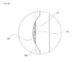
- FIG. 5 is a cross sectional view along the A-A′ line in FIG. 2 ;
- FIG. 6A is a schematic plan view showing the relation between the cover member and the conductive patterns in another embodiment of the light emitting device disclosed herein;
- FIG. 6B is a detail view of the portion surrounded by the dotted-line circle in FIG. 6A ;
- FIG. 7A is a schematic plan view showing the relation between the cover member and the conductive patterns in yet another embodiment of the light emitting device disclosed herein;
- FIG. 7B is a detail view of the portion surrounded by the dotted-line circle in FIG. 7A .
- the light emitting device 100 includes an element mounting board 10 consisting of a base 11 and a set of conductive patterns 12 having one or more element mounting areas 12 a and an external connector 12 b disposed on a main surface of the base 11 ; one or more light emitting elements 20 that are mounted on the one or more element mounting areas 12 a ; and a cover member 40 that covers the one or more light emitting elements 20 and the element mounting area 12 a .
- a set of the conductive patterns 12 include one or more first conductive layers 121 and second conductive layers 122 made of a different material from that of the first conductive layers 121 , in this order from the base 11 side.
- the element mounting areas 12 a have the first conductive layers 121 that are not covered by the second conductive layers 122 , and the external connectors 12 b each have outer edge exposed parts 12 e where at least a part of the outer edges of the first conductive layers 121 is exposed from each of the second conductive layers 122 , and said outer edge exposed parts 12 e are separated from the cover member 40 .
- the element mounting board 10 in this embodiment includes the base 11 and the set of conductive patterns 12 that are disposed on a main surface of the base 11 .
- the set of conductive patterns 12 each includes the element mounting area 12 a and the external connector 12 b .
- the conductive patterns 12 each includes the first conductive layer 121 and the second conductive layer 122 , which is made from a different material from that of the first conductive layer, in this order from the base 11 side.
- the element mounting areas 12 a include the first conductive layers 121 that is not covered by the second conductive layers 122 .
- the conductive patterns 12 include the element mounting areas 12 a , which is the area in which the one or more light emitting elements are mounted, and the external connectors 12 b , which are the areas in which power is supplied from the outside. Furthermore, the conductive patterns 12 include at least two conductive layers, namely, the first conductive layer 121 and the second conductive layer 122 , and at least part of the second conductive layer 122 is stacked on the first conductive layer.
- the one or more light emitting elements 20 are placed on the first conductive layers 121 located on the element mounting area 12 a .
- the external connector 12 b includes the first conductive layers 121 and the second conductive layers 122 , and the second conductive layers 122 located on the external connector 12 b is used as an external electrode of the light emitting device 100 to supply power from the outside.
- conductive layers made of different materials can be disposed on the set of conductive patterns 12 , with the first conductive layers 121 on the outermost surface of the element mounting areas, and the second conductive layers 122 on the outermost surface of the external power feed area.
- conductive layers that are respectively suited for the element joining material and for the external power feed member can be disposed on the outermost surfaces of the element mounting areas 12 a and the external connectors 12 b . Consequently, the light emitting elements can be joined more securely to the element mounting board, as can the external power feed member to the element mounting board.
- the base 11 can be a mounting board that is normally used for mounting the light emitting elements 20 , etc.
- Examples include mounting boards formed from glass, glass epoxy, thermoplastic resin, thermosetting resin, or another such resin, ceramic, paper phenol, paper epoxy, glass composite, low-temperature co-fired ceramic (LTCC), metal members in which the above materials are formed as insulating members, and so forth.
- LTCC low-temperature co-fired ceramic
- ceramics that have good thermal resistance and environmental resistance can be used to advantage.
- ceramic materials include alumina, aluminum nitride, and these ceramic materials may be combined with mullite, and a BT resin, glass epoxy, an epoxy resin, or another such insulating material.
- the shape and size of the base 11 can be suitably determined according to the design of the light emitting device.
- the base 11 may have a plate-like shape, and one that is flat on the front and back sides is preferable.
- the planar shape may be quadrangular, circular, elliptical, polyhedral, or the like, but a substantially rectangular shape is preferable from the standpoint of ease of processing.
- the element mounting board 10 in this embodiment includes at least a set of conductive patterns 12 on a main surface of the base 11 .
- the one or more light emitting elements 20 are connected above the conductive patterns 12 .
- the planar shape of the conductive patterns 12 on a main surface of the base 11 can be suitably set according to the design of the light emitting device.
- the set of conductive patterns 12 each include the one or more element mounting areas 12 a and the external connectors 12 b .
- the element mounting areas 12 a refers to an area in which the one or more light emitting elements 20 discussed below are mounted, and which are connected to the electrodes of the light emitting elements 20 .
- the element mounting areas 12 a includes not only the area in which the light emitting elements 20 are mounted, but also the area around it.
- the external connectors 12 b refer to an area that extends from the element mounting areas 12 a and that ensure electrical connection with the outside.
- the element mounting areas 12 a and the external connectors 12 b refer to mutually different areas in order for the above-mentioned functions to be realized, but the boundary between them in the element mounting board 10 need not be distinct.
- the element mounting areas 12 a may each include a surface shape that differs from that of the set of conductive patterns so as to correspond to the electrode shape, layout, and so forth of the light emitting elements 20 .
- the external connectors 12 b may each include mutually different shapes to make it easy to identify positive and negative.
- the planar shapes of the element mounting areas 12 a and the external connectors 12 b may be the same shapes for the set of patterns, but the different shapes for the set of patterns is preferable.
- the external connectors 12 b are preferably disposed near the edge of the base 11 (i.e., near the outer edge of the main surface on which the conductive patterns 12 are disposed).
- the external connectors may be disposed on a base that is substantially rectangular in plan view, (i) extending from the element mounting areas to near the edge of the base in a x direction, (ii) extending from the element mounting areas to near the edge of the base in the x direction, bending, and then extending along the edge of the base to the other edge of the base, (iii) extending from the element mounting areas to near the edge of the base in a different direction from the x direction, such as a y direction that is perpendicular to the x direction, or (iv) extending from the element mounting areas in the y direction to near the edge of the base, bending, and then extending along the edge of the base to another edge of the base.
- the external connectors near the edge of the base allows the power feed member, such as a wire, used for feeding power to the external connectors to have a shorter connection length, and allows power to be fed easily and surely.
- near the edge here means that the distance from the outer edge of the base main surface where the conductive patterns are disposed to the conductive patterns is in a range of 0.01 mm to 0.5 mm.
- the conductive patterns 12 are such that the one or more first conductive layers 121 and the second conductive layers 122 , which are made of a different material from that of the first conductive layers 121 , are stacked in this order from the base 11 side.
- the “different material” here in the case of a single-layer structure, includes a material in which some of the elements are the same but the rest of the elements are different, and in the case of a layered structure, encompasses a material in which some of the layers are the same but the rest of the layers are different, and a situation in which the stacking orders are different, etc.
- the element mounting areas 12 a include the first conductive layers 121 that is not covered by the second conductive layers 122 .
- the element mounting areas 12 a are such that the first conductive layers 121 that are each exposed from the second conductive layers 122 are disposed on all or part of the element mounting areas 12 a .
- the light emitting elements 20 are mounted on the first conductive layers 121 at the element mounting areas 12 a.
- the external connectors 12 b include the first conductive layers 121 and the second conductive layers 122 , in this order from the base 11 side.
- the external connectors 12 b further include outer edge exposed parts 12 e , in which part of the outer edge of the first conductive layers 121 are each exposed from the second conductive layers 122 .
- the second conductive layers 122 can be used for connecting an external power feed member in the secondary mounting of the light emitting device 100 .
- the outer edge exposed parts 12 e can be used for identifying the position of the light emitting face of the light emitting device 100 in the secondary mounting of the light emitting device 100 .
- the position of the light emitting face allows the position of the light emitting face to be identified more accurately.
- position identification accuracy may suffer as a result of dimensional tolerance, etc., in the formation of the second conductive layers 122 on the first conductive layers 121 .
- part of the outer edge of the first conductive layers 121 on which the light emitting elements 20 are mounted can be used for position identification during secondary mounting, therefore, the position of the light emitting face can be identified more accurately.
- the first conductive layers 121 are preferably covered by the second conductive layers 122 . Accordingly, the surface area of the second conductive layers 122 connected to an external power feed member can be increased in the external connectors 12 b.
- the outer edge exposed parts 12 e part of the outer edge of the first conductive layers 121 is used to identify position information about the light emitting elements 20 mounted on the first conductive layers 121 . Therefore, the outer edge exposed parts 12 e preferably include a characteristic point, such as the corners or sides constituting the outer edge of the first conductive layers 121 , in order to accurately identify the position of the outer edge exposed parts 12 e in the light emitting device 100 . More specifically, the outer edge exposed parts 12 e preferably include at least part of the sides constituting the outer edge of the first conductive layers 121 . It is even more preferable to include two adjacent sides, among the sides constituting the outer edge of the first conductive layers 121 .
- the outer edge exposed parts 12 e include the corners of the first conductive layers, it is possible to identify position information in at least two directions with a single outer edge exposed part, and the position of the light emitting face can be identified more accurately.
- the outer edge exposed parts 12 e more preferably are located at the corners of the outer edge of the external connectors 12 b . Providing the outer edge exposed parts 12 e at the corners of the external connectors 12 b makes it easier to identify the position of the outer edge exposed parts 12 e in the external connectors 12 b , and is also preferable because it is possible to provide a larger area of the second conductive layers used for connecting to an external power feed member.
- the surface area of the outer edge exposed parts 12 e in plan view (i.e., the surface area of the first conductive layers exposed from the second conductive layers in the external connectors 12 b ) can be suitably set according to the size of the light emitting device. For instance, it can be about 1/1000 to 1/10 the surface areas of the external connectors. More specifically, an example is about 20 ⁇ m to 200 ⁇ m.
- the shapes of the outer edge exposed parts in plan view may be the same, or the shapes may be mutually different.
- the first conductive layers 121 and the second conductive layers 122 can be formed, for example, as a stacked structure or a single layer of aluminum, gold, platinum, titanium, copper, palladium, rhodium, nickel, tungsten, molybdenum, chromium, silver, or other metal, or an alloy of these. Also, ITO or other conductive material other than a metal may be used.
- the element mounting areas 12 a include the first conductive layers 121 that are not covered by the second conductive layers 122 , and the light emitting elements 20 are mounted on the first conductive layers 121 .
- the outermost surfaces of the first conductive layers 121 preferably contain gold. Since the electrodes of the light emitting elements 20 usually employ gold, in the case that the outermost surfaces of the first conductive layers 121 are layers that contain gold, connection with the light emitting elements 20 is more reliable. A gold-gold connection realizes good reliability, so the connection portion is less likely to degrade even under the high voltage application condition, and a highly reliable connection can be maintained over an extended period.
- the first conductive layers 121 can be formed by a single-layer film of gold or a layered film in which AlSiCu/Ti/Pt/Au, Ti/Rh/Au, W/Pt/Au, Rh/Pt/Au, Ni/Pt/Au, Ti/Rh/Au, or the like are stacked from the base side.
- the total thickness of the first conductive layer 121 is preferably 1.0 ⁇ m or more, and more preferably 3.0 ⁇ m or more.
- the thickness of the gold is preferably at least 1.0 ⁇ m.
- the total thickness of the first conductive layer 121 is preferably about 10.0 ⁇ m or less. Such thickness allows the desired layer to be formed in a suitable amount of time, and increases in film formation time and material cost is likely to be suppressed.
- the external connectors 12 b include the first conductive layers 121 and the second conductive layers 122 , in this order from the base 11 side, and include the outer edge exposed parts 12 e where part of the outer edge of the first conductive layers 121 is exposed from the second conductive layer 122 .
- An external power feed member is connected to the second conductive layers of the external connectors.
- the outermost surface of the second conductive layers 122 are preferably layers that contain copper or aluminum, and are more preferably layers that contain aluminum.
- wires or other members made of aluminum or other material can be used for the power feed members carrying electricity to the external connectors 12 b .
- Aluminum is less expensive than gold, and is preferable as a power feed material because it can be easily joined with ultrasonic waves alone, without having to use heat treatment.
- the power feed member connected to the external connectors 12 b are preferably made of the same metal material as the outermost surfaces of the external connectors 12 b .
- the different metals diffuse into each other to form an alloy layer, but depending on the combination of metal materials, the alloy layer will become brittle as diffusion progresses, and this may lead to poor connection.
- alloying and degradation of the metal at the connection portion which is particularly attributable to the heat generated by the light emitting elements, can be avoided, thereby ensuring more reliable connection over an extended period.
- this can be formed by a single-layer film of aluminum or copper, or a layered film in which Ti/Al, Ti/Cu, Ni/Al, Ni/Cu, or the like are stacked from the first conductive layer side.
- the total thickness of the second conductive layer 122 is preferably 1.0 ⁇ m or more, and more preferably 3.0 ⁇ m or more.
- the thickness of the aluminum layer is preferably 2.0 ⁇ m or more, to take into account of peeling occurred by impact in joining of the power feed member.
- the total thickness of the second conductive layer is preferably about 10.0 ⁇ m or less, taking into account a suitable film formation time, material costs, and so forth.
- the element mounting board 10 may also include conductive patterns for making electrical connection with the light emitting elements 20 , according to the number of light emitting elements 20 to be mounted.
- one or more relay-use conductive patterns corresponding to the element mounting areas 12 a of the set of conductive patterns 12 may be arranged between the element mounting areas 12 a of the set of conductive patterns 12 .
- a plurality of light emitting elements may be disposed so as to be driven independently, depending on the shape of the set of conductive patterns 12 . Otherwise, the conductive patterns may be disposed so as to be driven in series, in parallel, or in a combination of these.
- the conductive patterns 12 need only be disposed at least on the front side of the base, but may also be disposed on the back side of the base along the lateral faces of the base or via through-holes in the base, etc.
- the conductive patterns can be formed by methods known in the art. For instance, one of the following methods (i) to (iii) can be used, or a method that combines parts of these can be used.
- a first conductive film constituting a first conductive layer is formed on a main surface of a base, and the first conductive film is formed into a specific shape by etching with a first conductive layer mask to form a first conductive layer.
- a second conductive film constituting a second conductive layer is formed over the base on which the first conductive layer has been formed, and the second conductive film is formed into a specific shape by etching with a second conductive layer mask to form a second conductive layer.
- the first conductive layer and the second conductive layer are formed in this order on a main surface of the base, and the first conductive layer mask and the second conductive layer mask are used to etch the second conductive layer and the first conductive layer in this order in to a specific shape.
- the first conductive film is formed on a main surface of a base using a first conductive layer mask that is open in the shape of the first conductive layer, and the first conductive film on the first conductive layer mask is removed by lift-off to form the first conductive layer with a specific shape.
- the second conductive layer mask that is open in the shape of the second conductive layer is formed on the base on which the first conductive layer was formed, the second conductive film is formed on this, and the second conductive film on the second conductive layer mask is removed by lift-off to form the second conductive layer with a specific shape.
- the first conductive film and the second conductive film can be formed by a known method, such as vapor deposition, sputtering, CVD, or ALD.
- a mask can be formed by photolithography, printing, or the like.
- light emitting elements 20 For the light emitting elements 20 , light emitting diodes are usually employed.
- composition, emission color and wavelength, size, number, and so forth of the light emitting elements 20 can be suitably selected to match the application.
- a nitride semiconductor In X Al Y Ga 1-X-Y N; 0 ⁇ X, 0 ⁇ Y, X+Y ⁇ L
- GaAlAs or AlInGaP can be used as a red light emitting element.
- the light emitting elements 20 are usually formed by laminating a semiconductor layer on a growth substrate (such as a sapphire substrate).
- the substrate may have rough surface that is joined to the semiconductor layer. This allows the critical angle when light emitted from the semiconductor layer hits the substrate to be varied intentionally, and allows light to be easily extracted to the outside of the substrate.
- the growth substrate may be removed from the light emitting elements 20 after the lamination of the semiconductor layer. This removal can be accomplished, for example, by polishing, LLO (laser lift off), or the like. Also, in the case that the growth substrate is removed, a mounting-use support substrate may be provided to the semiconductor layer.
- LLO laser lift off
- the light emitting elements 20 preferably include a set of positive and negative electrodes on the same surface. This allows the light emitting elements to be flip-chip mounted on the mounting board.
- the surface that is opposite the surface where the set of electrodes is formed serves as the main light extraction face.
- an electroconductive paste-like joining member such as solder, a thin-film joining member, or a bump-like joining member is used to electrically connect the light emitting elements to the conductive patterns on the base.
- the surface on which the set of electrodes is formed may serve as the main light extraction face.
- the light emitting elements 20 may employ one that a positive electrode is disposed on a surface on which a negative electrode is disposed.
- the light emitting elements have an opposing electrode structure in which the set of positive and negative electrodes are provided on opposite surfaces, the lower surface electrode is fixed to a conductive pattern on the base with a conductive member, and the upper surface electrode is connected to the base with a conductive wire or the like.
- the surface on the opposite side from the surface that is opposite the element mounting board of the light emitting elements 20 can be the upper surface, and the upper surface can be the main light extraction face.
- the outermost surfaces of the set of positive and negative electrodes of the light emitting elements 20 are preferably made of gold.
- Gold is chemically stable, ensuring reliable electrical connection over an extended period.
- the material can be the same as that of the first conductive layer, and in particular a gold-gold connection can be made, which affords connection with better reliability.
- a single light emitting device may include just one light emitting element 20 , or may include two or more.
- the light emitting elements are preferably arranged in order.
- the light emitting elements may, for example, be disposed in a single row, or may be disposed in a matrix.
- the number and planar shape of the light emitting elements can be suitably set according to the characteristics, size, and so forth of the light emitting device to be obtained.
- the arranged light emitting elements are preferably close to one another.
- the distance between light emitting elements is preferably shorter than the size of the light emitting elements on, for example, length along one side of one of the light emitting elements. For instance, about 30% or less of the size of the light emitting elements themselves is preferable, and even more preferably 20% or less.
- the mounting of the light emitting elements 20 on the element mounting board 10 is usually performed with a joining member 60 in between.
- the joining member here include solder based on tin-bismuth, tin-copper, tin-silver, gold-tin, or the like, alloys whose main components are gold and tin, alloys whose main components are gold and silicon, alloys whose main components are gold and germanium, and other such eutectic alloys, silver, gold, palladium, and other such conductive pastes, bumps, ACP, ACF, or other such anisotropic conductive materials, low-melting point braze materials, and conductive adhesive materials and/or conductive composite adhesive materials that are a combination of these.
- the light emitting elements 20 is mounted on the conductive patterns with a joining member 60 that contains gold, and even more preferable for each electrode of the one or more light emitting elements to be joined to the set of conductive patterns with a joining member that contains gold.
- the outermost surface of the first conductive layer is a layer that contains gold, using a joining member that contains gold will more reliably ensure a stable connection over an extended period of time.
- the cover member 40 reflects the light traveling toward some directions other than a direction to the upper surface of a light transmissive member 30 in the light emitting device 100 so that the light will be emitted from the upper surface of the light transmissive member 30 , and also covers the lateral surfaces of the light emitting elements 20 and the light transmissive member 30 and thereby protects the light emitting elements 20 from external force, dust, gas, and so forth.
- the cover member 40 is provided such that the upper surface of the light transmissive member 30 is exposed as the emission face of the light emitting device 100 , and so as to cover part of the upper surface of the element mounting board 10 as well as the light transmissive member 30 and the light emitting elements 20 .
- covering here includes that one or more other layers interposes between the cover member 40 and the light transmissive member 30 , the cover member 40 and the light emitting elements 20 , and the cover member 40 and the element mounting board 10 .
- other layers include an adhesive material 50 discussed below and an underfill or other embedded member.
- the adhesive material 50 is used when the upper surfaces of the light emitting elements are provided with a light transmissive member 30 that covers these light emitting element upper surfaces.
- the adhesive material 50 is preferably disposed so as not to bulge out from the area directly below the light transmissive member 30 .
- this embedded member is preferably a substance with good light reflectivity. In the case that the embedded member has high optical reflectivity, its interposed thickness can be set as desired.
- the cover member 40 disposed between the light emitting elements is preferably substantially flush with the upper surfaces of the light emitting elements.
- substantially flush means that a height difference of about ⁇ 10%, and preferably about ⁇ 5%, of the thickness of the cover member is allowable.
- the upper surface of the light transmissive member 30 serves as the light extraction face of the light emitting device 100
- the upper surface of the cover member is preferably substantially flush with the upper surface of the light transmissive member.
- the cover member disposed between the light transmissive members is preferably substantially flush with the upper surfaces of the light transmissive members.
- the shape of the cover member 40 can be suitably set according to the number of light emitting elements, the layout of the light emitting elements, and so forth. It is especially preferable for the planar shape to be rectangular or a shape that is similar to that. In plan view, part of the outer edge of the cover member 40 preferably coincides with the outer edge of the above-mentioned element mounting board 10 .
- the outer edge of the cover member 40 on the external connector side of the conductive patterns 12 on the element mounting board 10 is preferably parallel or substantially parallel to the outer edge of the element mounting board and the outer edge of the external connectors, such as the outer edge of the end extending in the x direction or the y direction.
- substantially parallel as used here means that tolerance of about ⁇ 10°, and preferably about ⁇ 5, from parallel is allowable.
- the boundary between the element mounting areas 12 a and the external connectors 12 b can be demarcated by the cover member 40 discussed below.
- the outer edge of the cover member 40 can be demarcated by the boundary between the element mounting areas 12 a and the external connectors 12 b . That is, the element mounting areas 12 a are each disposed on the upper surface of the light emitting device 100 and are integrally covered by the cover member 40 along with the lateral surfaces of the light emitting elements 20 and the light transmissive member 30 , while the external connectors 12 b are not covered by the cover member 40 .
- the surface of the first conduction layer 121 preferably has the wettability higher than that of the surface of the second conduction layer 122 .
- the cover member 40 is formed of a resin material or is bonded with a resin material, the resin component bleeding out from the resin material is less likely to wet and spread out over the external connectors 12 b.
- the outermost surface of the first conduction layer 121 is preferably a layer that contains gold.
- the surface of the first conductive layer in which gold is used for the outermost surface has good wettability with solder or the like, and has good connection reliability with the joining member 60 . Adversely, due to the good wettability, the resin composition bleeding out from the resin material tends to wet on and spread out over the surface. In the light emitting device 100 according to this embodiment, however, since the outer edge exposed parts 12 e of the first conduction layer 121 in the external connectors 12 b are separated from the cover member 40 , the resin in the cover member formation process is less likely to wet and spread out over the external connectors 12 b by running through the first conduction layer 121 .
- the first conduction layer 121 is preferably covered by the second conduction layer 122 except for the outer edge exposed parts 12 e . That is, the outermost surface of the conductive patterns 12 touching the outer edge of the cover member 40 is preferably the second conduction layer 122 .
- the outermost surface of the second conduction layer 122 is preferably a metal layer other than gold. In the case of metals other than gold, oxidation films tend to be formed on the surfaces of the metals in the air, and thus such metals on which oxidation films are formed tends to have poor wettability. Therefore, the resin composition is less likely to spread by disposing the second conductive layers at a position in contact with the outer edge of the cover member 40 .
- the resin composition is less likely to spread to the external connectors 12 b by disposing the first conduction layer 121 , which has higher wettability than the surface of the second conduction layer 122 , away from the outer edge of the cover member 40 .
- the poor join and so forth is less likely to occur between the external connectors and the power feed member caused by wetting and spreading of the resin composition during formation of the cover member.
- the cover member 40 can be formed of a material that is able to reflect the light emitted from the light emitting elements 20 . Consequently, the light emitted from the light emitting elements is reflected within the light emitting elements at the boundary between the light emitting elements 20 and the cover member 40 . As a result, the light propagates within the light emitting elements, and is emitted from the upper surfaces of the light emitting elements to the upper surface of the light transmissive member, and ultimately extracted to the outside.
- the cover member 40 can be formed using at least one light reflecting substance and a resin such as a silicone resin, a modified silicone resin, an epoxy resin, a modified epoxy resin, and an acrylic resin, or a hybrid resin containing one or more of these.
- a resin such as a silicone resin, a modified silicone resin, an epoxy resin, a modified epoxy resin, and an acrylic resin, or a hybrid resin containing one or more of these.
- light reflecting substances include titanium oxide, silicon oxide, zirconium oxide, potassium titanate, alumina, aluminum nitride, boron nitride, and mullite.
- the amount of light reflected and transmitted by the cover member 40 , etc. can be varied, so it can be suitably adjusted according to the characteristics of the light emitting device to be obtained and other such considerations.
- the content of the light reflecting substance is preferably 30 wt % or more.
- the cover member may be made of a material that dissipates heat in addition to reflecting light.
- the cover member preferably has the thermal conductivity of 0.2 W/m ⁇ K or more, and more preferably at least 1 W/m ⁇ K. Heat dissipation can be improved by setting the thermal conductivity high. Examples of such materials include boron nitride and aluminum nitride, which have high thermal conductivity.
- the phosphor may generate heat by Stokes loss, and this heat can lower light conversion efficiency.
- the cover member has high thermal conductivity, it will be able to efficiently dissipate the heat of the phosphor in the light transmissive member.
- the cover member can be formed, for example, by injection molding, potting, printing, transfer molding, compression molding, etc.
- the light transmissive member 30 is disposed on the upper surface side of the light emitting elements 20 .
- the light transmissive member 30 is joined to the upper surfaces of the light emitting elements.
- the light transmissive member 30 includes an upper surface and a lower surface, having a function that the light emitted from the light emitting elements is incident on the lower surface, and the upper surface serves as the light extraction face, and the light is emitted from the upper surface to the outside.
- the light transmissive member preferably transmits 60% or more of the light emitted from the light emitting elements, for example.
- the light transmissive member 30 preferably covers the entire upper surfaces of the light emitting elements 20 in order for the light emitted from the light emitting elements 20 to be extracted efficiently. That is, as seen from the upper surface side of the light transmissive member 30 , the light emitting elements 20 are preferably covered such that they are enveloped by the light transmissive member 30 .
- the light transmissive member 30 may cover the plurality of light emitting elements individually, or may cover the light emitting elements integrally.
- the outer peripheral surface of the light transmissive member 30 is preferably covered by the cover member 40 .
- the light transmissive member 30 can have a thickness about 50 ⁇ m to 300 ⁇ m.
- the upper surfaces of the light transmissive members are preferably flush or substantially flush with one another. This more effectively discourages interference between the light rays emitted from the lateral surfaces of the light transmissive members.
- the light transmissive member(s) may have upper surfaces in any of a variety of shapes, such as a projections-depressions shape, a curved surface, or a lens shape.
- the lower surface(s) of the light transmissive member is/are preferably parallel to the light extraction face(s) of the light emitting element(s).
- the light transmissive member 30 can contain a light scattering material, or a phosphor capable of converting the wavelength of at least part of the light incident from the light emitting elements 20 .
- a light transmissive member 30 containing a phosphor include a sintered phosphor, and a phosphor powder that is added to a resin, glass, or another inorganic substance.
- the sintered phosphor may be the product of sintering a phosphor alone, or may be formed by sintering a mixture of a phosphor and a sintering auxiliary.
- the sintering auxiliary When a mixture of a phosphor and a sintering auxiliary is sintered, the sintering auxiliary preferably employ silicon oxide, aluminum oxide, titanium oxide, or another inorganic material. This helps reduce deformation and discoloration of the sintering auxiliary by light or heat even though the light emitting elements 20 have a high output.
- the phosphor contained in the light transmissive member 30 can be one that can be excited by the light emitted by the light emitting elements 20 .
- one of the following specific examples can be used alone, or two or more types may be combined.
- These phosphors can be combined with a blue light emitting element or an ultraviolet light emitting element to manufacture light emitting devices of various colors (such as a white light emitting device).
- a blue light emitting element or an ultraviolet light emitting element to manufacture light emitting devices of various colors (such as a white light emitting device).
- the type and concentration of the phosphor contained in the light transmissive member are adjusted to obtain white light.
- the concentration of the phosphor is preferably about 5% to 50%, for example.
- the light transmissive member 30 is joined so as to cover the upper surfaces (i.e., the light extraction faces) of the light emitting elements 20 .
- This joining can be accomplished, for example, by compression bonding, sintering, bonding with a known adhesive such as an epoxy or silicone, bonding with an organic adhesive agent with a high reflective index, bonding with a low-melting point glass, or the like.
- the light transmissive member is usually disposed on the upper surfaces of the light emitting elements, but depending on its configuration, it may cover part of the external connectors and/or the element mounting areas of the conductive patterns. That is, it may cover part of the first conductive layers and/or part of the second conductive layers.
- embedded members that reflect light may be disposed between the base and the light emitting elements. This allows the light emitted downward from the light emitting elements to be reflected, thus increasing the luminous flux. Also, stress caused by the difference in the coefficient of thermal expansion between the light emitting elements and the base can be absorbed, or heat dissipation can be enhanced.
- These embedded members may be disposed integrally directly under the light emitting elements from the lateral surfaces of the light emitting elements, or the members directly under the light emitting elements may be partially separated from the members on the lateral surfaces.
- the embedded members disposed directly under the light emitting elements can be formed of a material selected from the material forming the cover member that covers the lateral surfaces of the light emitting elements.
- the embedded member may be formed of a different material from that of the cover member, but is preferably formed of the same material.
- a Zener diode or other such protective element may be mounted in the light emitting device disclosed herein. For instance, by disposing a protective element so as to be embedded in the cover member, this prevents the protective element to absorb or block light from the light emitting elements, thus the light extraction is less likely to be reduced.
- an element mounting board 210 provided in the light emitting device of Embodiment 2 according to the present disclosure.
- the element mounting board 210 of Embodiment 2 differs from the element mounting board 10 of Embodiment 1 in the position and shape of outer edge exposed parts 13 e of the external connectors 12 b.
- the outer edge exposed parts 13 e in Embodiment 2 are such that one side L 1 among the sides constituting the outer edge of the first conduction layer 121 is exposed from the second conduction layer 122 .
- each of the set of conductive patterns 12 includes three outer edge exposed parts 13 c . Because the conductive patterns 12 each include three of the outer edge exposed parts 13 e where parts of three of the sides constituting the outer edge of the first conduction layer 121 are exposed, the position can be identified by the three outer edge exposed parts in three directions. That is, in Embodiment 2, the outer edge exposed parts 13 e can be used to identify the position of the light emitting face in secondary mounting, thus mounting accuracy can be improved.
- an element mounting board 310 provided to the light emitting device of Embodiment 3 according to the present disclosure.
- the element mounting board 310 of Embodiment 3 differs from the light emitting device 100 of Embodiment 1 in the position and shape of outer edge exposed parts 14 e of the external connectors 12 b.
- the outer edge exposed parts 14 e of Embodiment 3 are such that three contiguous sides L 2 , L 3 , and L 4 among the sides constituting the outer edge of the first conduction layer 121 are exposed from the second conduction layer.
- each of the set of conductive patterns 12 includes two outer edge exposed parts 14 e . Because one of the outer edge exposed parts 14 e of the external connector 12 b includes the three contiguous sides L 2 , L 3 , and L 4 among the sides constituting the outer edge of the first conduction layer 121 , and corners located in between these sides, the position can be identified by a single outer edge exposed part 14 e in three directions. That is, in Embodiment 3, the outer edge exposed parts 14 e can be used to identify the position of the light emitting face in secondary mounting, thus mounting accuracy can be improved.
- the light emitting device of the present disclosure can be used for a variety of light sources employed in, for example, lighting, various kinds of indicators, interior and exterior lighting for vehicles, display, liquid crystal backlight lights, signaling devices, components installed in vehicles, and signage channel letters.
Landscapes
- Engineering & Computer Science (AREA)
- Microelectronics & Electronic Packaging (AREA)
- Power Engineering (AREA)
- Computer Hardware Design (AREA)
- Manufacturing & Machinery (AREA)
- Physics & Mathematics (AREA)
- Condensed Matter Physics & Semiconductors (AREA)
- General Physics & Mathematics (AREA)
- Led Device Packages (AREA)
Applications Claiming Priority (2)
| Application Number | Priority Date | Filing Date | Title |
|---|---|---|---|
| JP2016-108125 | 2016-05-31 | ||
| JP2016108125A JP6414141B2 (ja) | 2016-05-31 | 2016-05-31 | 発光装置 |
Publications (2)
| Publication Number | Publication Date |
|---|---|
| US20170345985A1 US20170345985A1 (en) | 2017-11-30 |
| US10276767B2 true US10276767B2 (en) | 2019-04-30 |
Family
ID=60418907
Family Applications (1)
| Application Number | Title | Priority Date | Filing Date |
|---|---|---|---|
| US15/608,006 Active 2037-08-17 US10276767B2 (en) | 2016-05-31 | 2017-05-30 | Light emitting device |
Country Status (2)
| Country | Link |
|---|---|
| US (1) | US10276767B2 (ja) |
| JP (1) | JP6414141B2 (ja) |
Cited By (1)
| Publication number | Priority date | Publication date | Assignee | Title |
|---|---|---|---|---|
| US20240093847A1 (en) * | 2021-02-08 | 2024-03-21 | Ichikoh Industries, Ltd. | Vehicle lamp |
Families Citing this family (9)
| Publication number | Priority date | Publication date | Assignee | Title |
|---|---|---|---|---|
| JP2019102715A (ja) * | 2017-12-06 | 2019-06-24 | スタンレー電気株式会社 | 半導体発光装置およびその製造方法 |
| DE102018101090A1 (de) * | 2018-01-18 | 2019-07-18 | Osram Opto Semiconductors Gmbh | Anzeigeelement, Anzeigevorrichtung und Verfahren zur Herstellung einer Kontaktstruktur bei einer Vielzahl von Anzeigeelementen |
| CN112119445A (zh) * | 2018-05-17 | 2020-12-22 | 株式会社半导体能源研究所 | 显示装置 |
| US11024785B2 (en) * | 2018-05-25 | 2021-06-01 | Creeled, Inc. | Light-emitting diode packages |
| US11335833B2 (en) | 2018-08-31 | 2022-05-17 | Creeled, Inc. | Light-emitting diodes, light-emitting diode arrays and related devices |
| JP6920619B2 (ja) | 2018-10-18 | 2021-08-18 | 日亜化学工業株式会社 | 発光装置 |
| JP7121312B2 (ja) * | 2020-03-26 | 2022-08-18 | 日亜化学工業株式会社 | 発光装置 |
| US11769862B2 (en) | 2020-03-26 | 2023-09-26 | Nichia Corporation | Light emitting device |
| CN116420046A (zh) * | 2020-08-21 | 2023-07-11 | 亮锐有限责任公司 | 多色照明设备、系统和制造方法 |
Citations (18)
| Publication number | Priority date | Publication date | Assignee | Title |
|---|---|---|---|---|
| US4423127A (en) * | 1980-12-29 | 1983-12-27 | Fujitsu Limited | Method of manufacturing a semiconductor device |
| US20020024981A1 (en) * | 2000-06-20 | 2002-02-28 | Tsuyoshi Tojo | Semiconductor laser |
| US20020067751A1 (en) * | 2000-11-28 | 2002-06-06 | Syuzo Ohbuchi | Semiconductor laser element and method of producing the same |
| US6525406B1 (en) * | 1999-10-15 | 2003-02-25 | Amkor Technology, Inc. | Semiconductor device having increased moisture path and increased solder joint strength |
| US20080006837A1 (en) * | 2006-07-07 | 2008-01-10 | Lg Electronics Inc. And Lg Innotek Co., Ltd | Sub-mount for mounting light emitting device and light emitting device package |
| US20100181365A1 (en) * | 2007-03-13 | 2010-07-22 | Kulicke And Soffa Industries, Inc. | Method of teaching eyepoints for wire bonding and related semiconductor processing operations |
| US7768617B2 (en) * | 2006-07-04 | 2010-08-03 | Semiconductor Energy Laboratory Co., Ltd. | Method for manufacturing a semiconductor device |
| US20120104452A1 (en) | 2010-10-29 | 2012-05-03 | Nichia Corporation | Light emitting apparatus and production method thereof |
| JP2012099544A (ja) | 2010-10-29 | 2012-05-24 | Nichia Chem Ind Ltd | 発光装置の製造方法 |
| JP2012099545A (ja) | 2010-10-29 | 2012-05-24 | Nichia Chem Ind Ltd | 発光装置及びその製造方法 |
| JP2012174808A (ja) | 2011-02-18 | 2012-09-10 | Nichia Chem Ind Ltd | 発光素子搭載用基板および発光装置 |
| US8319115B2 (en) * | 2008-09-22 | 2012-11-27 | Kyocera Slc Technologies Corporation | Wiring board and manufacturing method thereof |
| US20130015561A1 (en) * | 2011-07-11 | 2013-01-17 | Taiwan Semiconductor Manufacturing Company, Ltd. | Mechanisms for marking the orientation of a sawed die |
| JP2013026416A (ja) | 2011-07-20 | 2013-02-04 | Toyoda Gosei Co Ltd | 素子搭載基板及びこれを備えた発光装置 |
| US20130037968A1 (en) * | 2011-08-10 | 2013-02-14 | Renesas Electronics Corporation | Semiconductor apparatus and substrate |
| JP2015092622A (ja) | 2015-01-14 | 2015-05-14 | 日亜化学工業株式会社 | 発光装置 |
| US20150263247A1 (en) | 2014-03-17 | 2015-09-17 | Toyoda Gosei Co., Ltd. | Light Emitting Device |
| US9887333B2 (en) * | 2015-11-27 | 2018-02-06 | Nichia Corporation | Light emitting device and element mounting board |
Family Cites Families (5)
| Publication number | Priority date | Publication date | Assignee | Title |
|---|---|---|---|---|
| JP4539235B2 (ja) * | 2004-08-27 | 2010-09-08 | 日亜化学工業株式会社 | 半導体装置およびその製造方法 |
| US8272757B1 (en) * | 2005-06-03 | 2012-09-25 | Ac Led Lighting, L.L.C. | Light emitting diode lamp capable of high AC/DC voltage operation |
| JP2012015226A (ja) * | 2010-06-30 | 2012-01-19 | Toshiba Lighting & Technology Corp | 発光装置及び照明装置 |
| JP6519135B2 (ja) * | 2014-09-26 | 2019-05-29 | 日亜化学工業株式会社 | 発光装置及び発光装置用基板 |
| JP6411320B2 (ja) * | 2015-12-17 | 2018-10-24 | シャープ株式会社 | 発光装置および照明装置 |
-
2016
- 2016-05-31 JP JP2016108125A patent/JP6414141B2/ja active Active
-
2017
- 2017-05-30 US US15/608,006 patent/US10276767B2/en active Active
Patent Citations (22)
| Publication number | Priority date | Publication date | Assignee | Title |
|---|---|---|---|---|
| US4423127A (en) * | 1980-12-29 | 1983-12-27 | Fujitsu Limited | Method of manufacturing a semiconductor device |
| US6525406B1 (en) * | 1999-10-15 | 2003-02-25 | Amkor Technology, Inc. | Semiconductor device having increased moisture path and increased solder joint strength |
| US20020024981A1 (en) * | 2000-06-20 | 2002-02-28 | Tsuyoshi Tojo | Semiconductor laser |
| US20020067751A1 (en) * | 2000-11-28 | 2002-06-06 | Syuzo Ohbuchi | Semiconductor laser element and method of producing the same |
| US7768617B2 (en) * | 2006-07-04 | 2010-08-03 | Semiconductor Energy Laboratory Co., Ltd. | Method for manufacturing a semiconductor device |
| US20080006837A1 (en) * | 2006-07-07 | 2008-01-10 | Lg Electronics Inc. And Lg Innotek Co., Ltd | Sub-mount for mounting light emitting device and light emitting device package |
| US20100181365A1 (en) * | 2007-03-13 | 2010-07-22 | Kulicke And Soffa Industries, Inc. | Method of teaching eyepoints for wire bonding and related semiconductor processing operations |
| US8319115B2 (en) * | 2008-09-22 | 2012-11-27 | Kyocera Slc Technologies Corporation | Wiring board and manufacturing method thereof |
| US20140239320A1 (en) | 2010-10-29 | 2014-08-28 | Nichia Corporation | Light emitting apparatus and production method thereof |
| US20150270456A1 (en) | 2010-10-29 | 2015-09-24 | Nichia Corporation | Light emitting apparatus and production method thereof |
| US20160133800A1 (en) | 2010-10-29 | 2016-05-12 | Nichia Corporation | Light emitting apparatus and production method thereof |
| JP2012099544A (ja) | 2010-10-29 | 2012-05-24 | Nichia Chem Ind Ltd | 発光装置の製造方法 |
| JP2012099545A (ja) | 2010-10-29 | 2012-05-24 | Nichia Chem Ind Ltd | 発光装置及びその製造方法 |
| US20120104452A1 (en) | 2010-10-29 | 2012-05-03 | Nichia Corporation | Light emitting apparatus and production method thereof |
| JP2012174808A (ja) | 2011-02-18 | 2012-09-10 | Nichia Chem Ind Ltd | 発光素子搭載用基板および発光装置 |
| US20130015561A1 (en) * | 2011-07-11 | 2013-01-17 | Taiwan Semiconductor Manufacturing Company, Ltd. | Mechanisms for marking the orientation of a sawed die |
| JP2013026416A (ja) | 2011-07-20 | 2013-02-04 | Toyoda Gosei Co Ltd | 素子搭載基板及びこれを備えた発光装置 |
| US20130037968A1 (en) * | 2011-08-10 | 2013-02-14 | Renesas Electronics Corporation | Semiconductor apparatus and substrate |
| US20150263247A1 (en) | 2014-03-17 | 2015-09-17 | Toyoda Gosei Co., Ltd. | Light Emitting Device |
| JP2015177120A (ja) | 2014-03-17 | 2015-10-05 | 豊田合成株式会社 | 発光装置 |
| JP2015092622A (ja) | 2015-01-14 | 2015-05-14 | 日亜化学工業株式会社 | 発光装置 |
| US9887333B2 (en) * | 2015-11-27 | 2018-02-06 | Nichia Corporation | Light emitting device and element mounting board |
Cited By (1)
| Publication number | Priority date | Publication date | Assignee | Title |
|---|---|---|---|---|
| US20240093847A1 (en) * | 2021-02-08 | 2024-03-21 | Ichikoh Industries, Ltd. | Vehicle lamp |
Also Published As
| Publication number | Publication date |
|---|---|
| US20170345985A1 (en) | 2017-11-30 |
| JP2017216315A (ja) | 2017-12-07 |
| JP6414141B2 (ja) | 2018-10-31 |
Similar Documents
| Publication | Publication Date | Title |
|---|---|---|
| US10276767B2 (en) | Light emitting device | |
| US10367129B2 (en) | Light emitting device | |
| US10141491B2 (en) | Method of manufacturing light emitting device | |
| TWI783143B (zh) | 發光裝置 | |
| JP6399017B2 (ja) | 発光装置 | |
| US10629783B2 (en) | Light emitting device | |
| JP6481559B2 (ja) | 発光装置 | |
| US9887333B2 (en) | Light emitting device and element mounting board | |
| US10991859B2 (en) | Light-emitting device and method of manufacturing the same | |
| JP6511887B2 (ja) | 発光装置 | |
| JP6579159B2 (ja) | 発光装置 | |
| JP6326830B2 (ja) | 発光装置及びそれを備える照明装置 | |
| JP6724639B2 (ja) | 発光装置 | |
| JP7208495B2 (ja) | 光源装置 | |
| US10330852B2 (en) | Light-emitting device | |
| US11769862B2 (en) | Light emitting device | |
| JP6773166B2 (ja) | 発光装置 | |
| JP2022007882A (ja) | 発光装置 | |
| US10193032B2 (en) | Method for manufacturing light emitting device | |
| US11152552B2 (en) | Light emitting device | |
| JP2021097170A (ja) | 発光素子及び発光装置 | |
| JP2018182352A (ja) | 発光装置 | |
| JP6947997B2 (ja) | 発光装置 | |
| JP2022055733A (ja) | 発光装置の製造方法及び発光装置 |
Legal Events
| Date | Code | Title | Description |
|---|---|---|---|
| AS | Assignment |
Owner name: NICHIA CORPORATION, JAPAN Free format text: ASSIGNMENT OF ASSIGNORS INTEREST;ASSIGNOR:IDE, YOSHIYUKI;REEL/FRAME:042533/0886 Effective date: 20170526 |
|
| STPP | Information on status: patent application and granting procedure in general |
Free format text: PUBLICATIONS -- ISSUE FEE PAYMENT VERIFIED |
|
| STCF | Information on status: patent grant |
Free format text: PATENTED CASE |
|
| MAFP | Maintenance fee payment |
Free format text: PAYMENT OF MAINTENANCE FEE, 4TH YEAR, LARGE ENTITY (ORIGINAL EVENT CODE: M1551); ENTITY STATUS OF PATENT OWNER: LARGE ENTITY Year of fee payment: 4 |