US10249231B2 - Display device and optical compensation method of a display device - Google Patents
Display device and optical compensation method of a display device Download PDFInfo
- Publication number
- US10249231B2 US10249231B2 US15/389,997 US201615389997A US10249231B2 US 10249231 B2 US10249231 B2 US 10249231B2 US 201615389997 A US201615389997 A US 201615389997A US 10249231 B2 US10249231 B2 US 10249231B2
- Authority
- US
- United States
- Prior art keywords
- grayscale value
- luminance
- target luminance
- display device
- pixel
- Prior art date
- Legal status (The legal status is an assumption and is not a legal conclusion. Google has not performed a legal analysis and makes no representation as to the accuracy of the status listed.)
- Active, expires
Links
Images


Classifications
-
- G—PHYSICS
- G09—EDUCATION; CRYPTOGRAPHY; DISPLAY; ADVERTISING; SEALS
- G09G—ARRANGEMENTS OR CIRCUITS FOR CONTROL OF INDICATING DEVICES USING STATIC MEANS TO PRESENT VARIABLE INFORMATION
- G09G3/00—Control arrangements or circuits, of interest only in connection with visual indicators other than cathode-ray tubes
- G09G3/20—Control arrangements or circuits, of interest only in connection with visual indicators other than cathode-ray tubes for presentation of an assembly of a number of characters, e.g. a page, by composing the assembly by combination of individual elements arranged in a matrix no fixed position being assigned to or needed to be assigned to the individual characters or partial characters
- G09G3/22—Control arrangements or circuits, of interest only in connection with visual indicators other than cathode-ray tubes for presentation of an assembly of a number of characters, e.g. a page, by composing the assembly by combination of individual elements arranged in a matrix no fixed position being assigned to or needed to be assigned to the individual characters or partial characters using controlled light sources
- G09G3/30—Control arrangements or circuits, of interest only in connection with visual indicators other than cathode-ray tubes for presentation of an assembly of a number of characters, e.g. a page, by composing the assembly by combination of individual elements arranged in a matrix no fixed position being assigned to or needed to be assigned to the individual characters or partial characters using controlled light sources using electroluminescent panels
- G09G3/32—Control arrangements or circuits, of interest only in connection with visual indicators other than cathode-ray tubes for presentation of an assembly of a number of characters, e.g. a page, by composing the assembly by combination of individual elements arranged in a matrix no fixed position being assigned to or needed to be assigned to the individual characters or partial characters using controlled light sources using electroluminescent panels semiconductive, e.g. using light-emitting diodes [LED]
- G09G3/3208—Control arrangements or circuits, of interest only in connection with visual indicators other than cathode-ray tubes for presentation of an assembly of a number of characters, e.g. a page, by composing the assembly by combination of individual elements arranged in a matrix no fixed position being assigned to or needed to be assigned to the individual characters or partial characters using controlled light sources using electroluminescent panels semiconductive, e.g. using light-emitting diodes [LED] organic, e.g. using organic light-emitting diodes [OLED]
- G09G3/3225—Control arrangements or circuits, of interest only in connection with visual indicators other than cathode-ray tubes for presentation of an assembly of a number of characters, e.g. a page, by composing the assembly by combination of individual elements arranged in a matrix no fixed position being assigned to or needed to be assigned to the individual characters or partial characters using controlled light sources using electroluminescent panels semiconductive, e.g. using light-emitting diodes [LED] organic, e.g. using organic light-emitting diodes [OLED] using an active matrix
-
- G—PHYSICS
- G09—EDUCATION; CRYPTOGRAPHY; DISPLAY; ADVERTISING; SEALS
- G09G—ARRANGEMENTS OR CIRCUITS FOR CONTROL OF INDICATING DEVICES USING STATIC MEANS TO PRESENT VARIABLE INFORMATION
- G09G3/00—Control arrangements or circuits, of interest only in connection with visual indicators other than cathode-ray tubes
- G09G3/20—Control arrangements or circuits, of interest only in connection with visual indicators other than cathode-ray tubes for presentation of an assembly of a number of characters, e.g. a page, by composing the assembly by combination of individual elements arranged in a matrix no fixed position being assigned to or needed to be assigned to the individual characters or partial characters
- G09G3/2092—Details of a display terminals using a flat panel, the details relating to the control arrangement of the display terminal and to the interfaces thereto
-
- G—PHYSICS
- G09—EDUCATION; CRYPTOGRAPHY; DISPLAY; ADVERTISING; SEALS
- G09G—ARRANGEMENTS OR CIRCUITS FOR CONTROL OF INDICATING DEVICES USING STATIC MEANS TO PRESENT VARIABLE INFORMATION
- G09G3/00—Control arrangements or circuits, of interest only in connection with visual indicators other than cathode-ray tubes
- G09G3/20—Control arrangements or circuits, of interest only in connection with visual indicators other than cathode-ray tubes for presentation of an assembly of a number of characters, e.g. a page, by composing the assembly by combination of individual elements arranged in a matrix no fixed position being assigned to or needed to be assigned to the individual characters or partial characters
- G09G3/22—Control arrangements or circuits, of interest only in connection with visual indicators other than cathode-ray tubes for presentation of an assembly of a number of characters, e.g. a page, by composing the assembly by combination of individual elements arranged in a matrix no fixed position being assigned to or needed to be assigned to the individual characters or partial characters using controlled light sources
- G09G3/30—Control arrangements or circuits, of interest only in connection with visual indicators other than cathode-ray tubes for presentation of an assembly of a number of characters, e.g. a page, by composing the assembly by combination of individual elements arranged in a matrix no fixed position being assigned to or needed to be assigned to the individual characters or partial characters using controlled light sources using electroluminescent panels
- G09G3/32—Control arrangements or circuits, of interest only in connection with visual indicators other than cathode-ray tubes for presentation of an assembly of a number of characters, e.g. a page, by composing the assembly by combination of individual elements arranged in a matrix no fixed position being assigned to or needed to be assigned to the individual characters or partial characters using controlled light sources using electroluminescent panels semiconductive, e.g. using light-emitting diodes [LED]
- G09G3/3208—Control arrangements or circuits, of interest only in connection with visual indicators other than cathode-ray tubes for presentation of an assembly of a number of characters, e.g. a page, by composing the assembly by combination of individual elements arranged in a matrix no fixed position being assigned to or needed to be assigned to the individual characters or partial characters using controlled light sources using electroluminescent panels semiconductive, e.g. using light-emitting diodes [LED] organic, e.g. using organic light-emitting diodes [OLED]
-
- G—PHYSICS
- G09—EDUCATION; CRYPTOGRAPHY; DISPLAY; ADVERTISING; SEALS
- G09G—ARRANGEMENTS OR CIRCUITS FOR CONTROL OF INDICATING DEVICES USING STATIC MEANS TO PRESENT VARIABLE INFORMATION
- G09G2310/00—Command of the display device
- G09G2310/08—Details of timing specific for flat panels, other than clock recovery
-
- G—PHYSICS
- G09—EDUCATION; CRYPTOGRAPHY; DISPLAY; ADVERTISING; SEALS
- G09G—ARRANGEMENTS OR CIRCUITS FOR CONTROL OF INDICATING DEVICES USING STATIC MEANS TO PRESENT VARIABLE INFORMATION
- G09G2320/00—Control of display operating conditions
- G09G2320/02—Improving the quality of display appearance
- G09G2320/0233—Improving the luminance or brightness uniformity across the screen
-
- G—PHYSICS
- G09—EDUCATION; CRYPTOGRAPHY; DISPLAY; ADVERTISING; SEALS
- G09G—ARRANGEMENTS OR CIRCUITS FOR CONTROL OF INDICATING DEVICES USING STATIC MEANS TO PRESENT VARIABLE INFORMATION
- G09G2320/00—Control of display operating conditions
- G09G2320/02—Improving the quality of display appearance
- G09G2320/0271—Adjustment of the gradation levels within the range of the gradation scale, e.g. by redistribution or clipping
- G09G2320/0276—Adjustment of the gradation levels within the range of the gradation scale, e.g. by redistribution or clipping for the purpose of adaptation to the characteristics of a display device, i.e. gamma correction
-
- G—PHYSICS
- G09—EDUCATION; CRYPTOGRAPHY; DISPLAY; ADVERTISING; SEALS
- G09G—ARRANGEMENTS OR CIRCUITS FOR CONTROL OF INDICATING DEVICES USING STATIC MEANS TO PRESENT VARIABLE INFORMATION
- G09G2320/00—Control of display operating conditions
- G09G2320/02—Improving the quality of display appearance
- G09G2320/029—Improving the quality of display appearance by monitoring one or more pixels in the display panel, e.g. by monitoring a fixed reference pixel
-
- G—PHYSICS
- G09—EDUCATION; CRYPTOGRAPHY; DISPLAY; ADVERTISING; SEALS
- G09G—ARRANGEMENTS OR CIRCUITS FOR CONTROL OF INDICATING DEVICES USING STATIC MEANS TO PRESENT VARIABLE INFORMATION
- G09G2320/00—Control of display operating conditions
- G09G2320/06—Adjustment of display parameters
- G09G2320/0626—Adjustment of display parameters for control of overall brightness
- G09G2320/0646—Modulation of illumination source brightness and image signal correlated to each other
-
- G—PHYSICS
- G09—EDUCATION; CRYPTOGRAPHY; DISPLAY; ADVERTISING; SEALS
- G09G—ARRANGEMENTS OR CIRCUITS FOR CONTROL OF INDICATING DEVICES USING STATIC MEANS TO PRESENT VARIABLE INFORMATION
- G09G2320/00—Control of display operating conditions
- G09G2320/06—Adjustment of display parameters
- G09G2320/0673—Adjustment of display parameters for control of gamma adjustment, e.g. selecting another gamma curve
-
- G—PHYSICS
- G09—EDUCATION; CRYPTOGRAPHY; DISPLAY; ADVERTISING; SEALS
- G09G—ARRANGEMENTS OR CIRCUITS FOR CONTROL OF INDICATING DEVICES USING STATIC MEANS TO PRESENT VARIABLE INFORMATION
- G09G2320/00—Control of display operating conditions
- G09G2320/06—Adjustment of display parameters
- G09G2320/0693—Calibration of display systems
Definitions
- Example embodiments relate to a display device.
- An organic light emitting display device includes pixels, and each of the pixels includes an organic light emitting diode and a thin film transistor which drives the organic light emitting diode.
- the thin film transistor may be formed through a crystallization process (e.g., a melting process and a solidification process) of a low-temperature poly-silicon (LTPS).
- LTPS low-temperature poly-silicon
- thin film transistors may have uneven characteristics (e.g., uneven current-voltage characteristics) due to the crystallization process.
- An optical compensation method for compensating a grayscale value such that the pixel emits light having a certain or desired luminance despite uneven or varying characteristics among the thin film transistors.
- the optical compensation method can compensate a grayscale value when the pixel emits light having a relatively high luminance; however, the optical compensation method cannot or cannot adequately compensate a grayscale value when the pixel emits light having a relatively low luminance because the optical compensation method cannot increase the grayscale value over a maximum grayscale value.
- a stain phenomenon e.g., a mottled phenomenon, a dappled phenomenon, a variegated phenomenon, a parti-colored phenomenon, a spotted phenomenon
- a stain phenomenon occurs on a display panel when input image data including a high grayscale value (e.g., the maximum grayscale value) is provided to the display device.
- Some example embodiments provide an emission driver that can finely control a light emission time of pixels.
- Some example embodiments provide a display device including the emission driver.
- an optical compensation method for a display device including a pixel includes: providing test data having a first grayscale value to the display device; measuring a luminance of the pixel which emits light based on the test data; and calculating a compensation grayscale value based on a second target luminance and the measured luminance of the pixel.
- the second target luminance is lower than a first target luminance which is set based on the first grayscale value.
- the first grayscale value may be a maximum grayscale value from among grayscale values which are used in the display device, and the first target luminance may be determined based on a grayscale-luminance characteristic of the pixel and the first grayscale value.
- the second target luminance may be lower than the first target luminance by B nits, where B is a positive integer.
- the compensation grayscale value may be a grayscale value difference between the first grayscale value and a second grayscale value, and the pixel may be configured to emit light having a second target luminance based on the second grayscale value.
- the calculating the compensation grayscale value of the pixel may include: calculating a luminance error between the second target luminance and the measured luminance; and calculating the compensation grayscale value based on the second target luminance, the luminance error, and the first grayscale value.
- the compensation grayscale value may be proportional to the luminance error.
- the optical compensation method may further include storing the compensation grayscale value in a memory device in the display device.
- the optical compensation method may further include performing a second multi-time program (MTP) based on the first grayscale value and the first target luminance.
- MTP multi-time program
- the performing the second multi-time program may include: providing the test data to the display device; re-measuring the luminance of the pixel which emits light based on a first compensated grayscale value which is generated by compensating the first grayscale value by the compensation grayscale value; calculating a luminance difference between the re-measured luminance and the first target luminance; and when the luminance difference exceeds a reference value, changing a first gamma voltage corresponding to the first compensated grayscale value.
- the performing the second multi-time program may further include: repeating each of the step of providing the test data to the display device through the step of changing the first gamma voltage; and when the luminance difference is lower than the reference value, storing the first gamma voltage.
- an optical compensation method for a display device including a pixel includes: performing a first multi-time program (MTP) based on a third target luminance and a first grayscale value; providing test data having the first grayscale value to the display device; measuring a luminance of the pixel based on the test data; and calculating a compensation grayscale value of the pixel based on a first target luminance and the measured luminance of the pixel.
- the first target luminance is determined based on the first grayscale value, and the third target luminance is higher than the first target luminance.
- the first grayscale value may be a maximum grayscale value from among grayscale values which are used in the display device, and the first target luminance may be determined based on a grayscale-luminance characteristic of the pixel and the first grayscale value.
- the third target luminance may be higher than the first target luminance by C nits, where C is a positive integer.
- the compensation grayscale value may be to compensate the first grayscale value for the pixel to emit light having the first target luminance.
- the calculating the compensation grayscale value of the pixel may include: calculating a luminance error between the first target luminance and the measured luminance; and calculating the compensation grayscale value based on the first target luminance, the luminance error, and the first grayscale value.
- the optical compensation method may further include storing the compensation grayscale value in a memory device in the display device.
- a display device includes a display panel including a pixel; a memory device configured to store a compensation grayscale value to compensate a first grayscale value of input data such that the pixel emits light having a first target luminance based on the first grayscale value; a timing controller configured to operate in a normal mode and in a compensation mode, the timing controller being further configured to generate a first compensated grayscale value by compensating the first grayscale value based on the compensation grayscale value in the compensation mode; and a data driver configured to generate a data signal based on the first compensated grayscale value.
- the pixel when the timing controller is in the compensation mode, the pixel may emit light having the first target luminance based on the first compensated grayscale value.
- the timing controller may be further configured to determine whether or not the first compensated grayscale value is equal to the first grayscale value.
- the pixel when the timing controller is in the normal mode, the pixel may emit light having a second target luminance based on the first compensated grayscale value, and the second target luminance may be lower than the first target luminance.
- An optical compensation method of a display device may eliminate or substantially eliminate (e.g., remove or prevent) a stain phenomenon of a display panel by calculating a compensation grayscale value based on a grayscale value (e.g., a maximum grayscale value) and a second target luminance that is lower than a first target luminance based on the grayscale value, and by performing a multi-time program (e.g., a post-MTP) based on the grayscale value and the first target luminance.
- a grayscale value e.g., a maximum grayscale value
- a second target luminance that is lower than a first target luminance based on the grayscale value
- a multi-time program e.g., a post-MTP
- an optical compensation method of a display device may provide a simplified optical compensation process by performing a multi-time program (e.g., a pre-MTP) based on the grayscale value (e.g., the maximum grayscale value) and a third target luminance that is higher than a first target luminance based on the grayscale value, and by calculating a compensation grayscale value based on the grayscale value and the first target luminance.
- a multi-time program e.g., a pre-MTP
- the grayscale value e.g., the maximum grayscale value
- a third target luminance that is higher than a first target luminance based on the grayscale value
- a display device may have improved display quality (e.g., a quality of a displayed image may be improved) by using a compensation grayscale value that is generated by the optical compensation method.
- FIG. 1 is a block diagram of a display device according to one or more example embodiments.
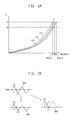
- FIG. 2A is a graph of an example gamma characteristic of a pixel included in the display device shown in FIG. 1 .
- FIG. 2B is a graph of an example luminance of a pixel included in the display device shown in FIG. 1 .
- FIG. 2C is a graph of an example gamma characteristic of a pixel included in the display device shown in FIG. 1 .
- FIG. 3 is a block diagram of a timing controller included in the display device shown in FIG. 1 .
- FIG. 4 is a flow diagram of an optical compensation method of a display device according to one or more example embodiments.
- FIG. 5 is a flow diagram of a second multi-time program included in the optical compensation method illustrated in FIG. 4 .
- FIG. 6 is a diagram illustrating the second multi-time program included in the optical compensation method illustrated in FIG. 4 .
- FIG. 7 is a flow diagram of an optical compensation method of a display device according to one or more example embodiments.
- FIG. 8A is a graph of an exemplary first multi-time program included in the optical compensation method illustrated in FIG. 7 .
- FIG. 8B is a graph of an incorrectly set gamma characteristic curve to be used in the method illustrated in FIG. 7 .
- the term “and/or” includes any and all combinations of one or more of the associated listed items. Further, the use of “may” when describing embodiments of the present invention relates to “one or more embodiments of the present invention.” Expressions, such as “at least one of,” when preceding a list of elements, modify the entire list of elements and do not modify the individual elements of the list. Also, the term “exemplary” is intended to refer to an example or illustration. As used herein, the terms “use,” “using,” and “used” may be considered synonymous with the terms “utilize,” “utilizing,” and “utilized,” respectively.
- first, second, third, etc. may be used herein to describe various elements, components, regions, layers, and/or sections, these elements, components, regions, layers, and/or sections should not be limited by these terms. These terms are used to distinguish one element, component, region, layer, or section from another element, component, region, layer, or section. Thus, a first element, component, region, layer, or section discussed below could be termed a second element, component, region, layer, or section without departing from the teachings of example embodiments. In the figures, dimensions of the various elements, layers, etc. may be exaggerated for clarity of illustration.
- spatially relative terms such as “beneath,” “below,” “lower,” “above,” “upper,” and the like, may be used herein for ease of description to describe one element or feature's relationship to another element(s) or feature(s) as illustrated in the figures. It will be understood that the spatially relative terms are intended to encompass different orientations of the device in use or operation in addition to the orientation depicted in the figures. For example, if the device in the figures is turned over, elements described as “below” or “beneath” other elements or features would then be oriented “above” or “over” the other elements or features. Thus, the term “below” may encompass both an orientation of above and below. The device may be otherwise oriented (rotated 90 degrees or at other orientations), and the spatially relative descriptors used herein should be interpreted accordingly.
- the scan driver, the timing controller, the data driver and/or any other relevant devices or components according to embodiments of the present invention described herein may be implemented utilizing any suitable hardware, firmware (e.g., an application-specific integrated circuit), software, and/or a suitable combination of software, firmware, and hardware.
- the various components of the scan driver, the timing controller, and/or the data driver may be formed on one integrated circuit (IC) chip or on separate IC chips.
- the various components of the scan driver, the timing controller, and/or the data driver may be implemented on a flexible printed circuit film, a tape carrier package (TCP), a printed circuit board (PCB), or formed on a same substrate as the scan driver, the timing controller, and/or the data driver.
- the various components of the scan driver, the timing controller, and/or the data driver may be a process or thread, running on one or more processors, in one or more computing devices, executing computer program instructions and interacting with other system components for performing the various functionalities described herein.
- the computer program instructions are stored in a memory which may be implemented in a computing device using a standard memory device, such as, for example, a random access memory (RAM).
- the computer program instructions may also be stored in other non-transitory computer readable media such as, for example, a CD-ROM, flash drive, or the like.
- FIG. 1 is a block diagram of a display device according to one or more example embodiments.
- a display device 100 may include a display panel 110 , a scan driver 120 , a timing controller 130 , and a data driver 140 .
- the display device 100 may display an image based on image data provided from an external component.
- the display device 100 may be an organic light emitting display device.
- the display panel 110 may include scan lines S 1 through Sn, data lines D 1 through Dm, and pixels 111 , where each of m and n is an integer greater than or equal to two.
- the pixels 111 may be disposed at cross-regions of the scan lines S 1 through Sn and the data lines D 1 through Dm, respectively.
- Each of the pixels 111 may store data (e.g., a data signal) in response to a scan signal and may emit light based on the stored data.
- the scan driver 120 may generate the scan signal based on a scan driving control signal SCS.
- the scan driving control signal SCS may be provided from the timing controller 130 to the scan driver 120 .
- the scan driving control signal SCS may include a start pulse and clock signals, and the scan driver 120 may include a shift register for sequentially generating the scan signal corresponding to the start pulse and the clock signals.
- the timing controller 130 may control the scan driver 120 and the data driver 140 .
- the timing controller 130 may generate the scan driving control signal SCS and a data driving control signal DCS and may control the scan driver 120 and the data driver 140 based on these generated signals.
- the timing controller 130 may include a first mode (e.g., a normal mode) and a second mode (e.g., a compensation mode).
- the timing controller 130 may generate second data DATA 2 (e.g., a second data signal) based on first data DATA 1 (e.g., a first data signal).
- first data DATA 1 e.g., a first data signal
- the timing controller 130 may generate the second data DATA 2 , which is substantially the same as the first data DATA 1 .
- the timing controller 130 may generate the second data DATA 2 by compensating (e.g., adjusting) the first data DATA 1 based on a compensation grayscale value.
- the compensation grayscale value is a grayscale value for compensating a certain grayscale value such that the pixels 111 each emit light having a certain target luminance based on the certain grayscale value.
- the compensation grayscale value is a grayscale value for compensating a first grayscale value (e.g., a maximum grayscale value) such that the pixels 111 each emit light having a first target luminance (e.g., a maximum luminance) based on the first grayscale value.
- the timing controller 130 may generate a first compensated grayscale value by compensating the first grayscale value based on the compensation value, and the pixels 111 may emit light having the first target luminance based on the first compensated grayscale value.
- the timing controller 130 may determine or set the compensated grayscale value to be equal to the first grayscale value in the first mode (e.g., when the first mode is selected). For example, the timing controller 130 may generate the second data DATA 2 that is substantially the same as the first data DATA 1 in the first mode. In the first mode, the pixels 111 may emit light having another luminance (e.g., a second target luminance which is lower than the first target luminance) that is different from the first target luminance based on the first grayscale value included in the first data DATA 1 .
- another luminance e.g., a second target luminance which is lower than the first target luminance
- the timing controller 130 may include a memory device for storing the compensation grayscale value.
- the memory device may include (e.g., may store) the first compensation grayscale value for compensating the first grayscale value.
- the first grayscale value may be a maximum grayscale value (e.g., a grayscale value of 255 from among grayscale values of 0 through 255) used in the display device 100 .
- the timing controller 130 may generate a second compensated grayscale value for a certain grayscale value by interpolating the first compensation grayscale value. For example, the timing controller 130 may calculate the second compensated grayscale value of minus 5 ( ⁇ 5) for compensating a grayscale value of 127 by interpolating a reference compensation grayscale value of 0 and the first compensation grayscale value of minus 10 ( ⁇ 10), where the reference compensation grayscale value of 0 is to compensate a grayscale value of 0, and the first compensation grayscale value of minus 10 ( ⁇ 10) is to compensate a grayscale value of 127.
- the data driver 140 may generate the data signal based on the second data DATA 2 , and the data driver 140 may provide the data signal to the display panel 110 (e.g., to the pixels 111 ) in response to the data driving control signal DCS.
- the data driver 140 may include a gamma correction value.
- the gamma correction value may be a voltage for compensating a gamma voltage (e.g., the data signal) provided to a certain pixel such that the certain pixel may emit light having a certain luminance based on a certain grayscale value.
- the gamma correction value may be set by a multi-time program (“MTP”) (e.g., set through a multi-time program).
- MTP multi-time program
- the gamma correction value may be set with respect to a pixel which is (or pixels which are) located at a center of the display panel 110 during a manufacturing process of the display panel 110 such that a gamma characteristic curve of the pixel or pixels may be the same as or substantially the same as a gamma characteristic curve of a reference pixel.
- the data driver 140 may generate a compensated gamma voltage based on the gamma correction value and the gamma characteristic curve of the reference pixel.
- the display device 100 may further include a power supply (e.g., a power supplier).
- the power supply may generate a driving voltage to drive the display device 100 .
- the driving voltage may include a first power voltage ELVDD and a second power voltage ELVSS.
- the first power voltage ELVDD may be greater than (higher than) the second power voltage ELVSS.
- the display device 100 may include (e.g., store) a compensation grayscale value for the first grayscale value (e.g., a maximum grayscale value), may compensate the first data DATA 1 based on the compensation grayscale value, and may display an image based on the compensated first data DATA 1 (e.g., the second data DATA 2 ). Therefore, the display device 100 may eliminate or reduce the occurrence or severity of a luminance stain phenomenon which occurs at a certain grayscale region (e.g., at a relatively high grayscale region) and, thus, may improve a display quality.
- a compensation grayscale value for the first grayscale value e.g., a maximum grayscale value
- the display device 100 may eliminate or reduce the occurrence or severity of a luminance stain phenomenon which occurs at a certain grayscale region (e.g., at a relatively high grayscale region) and, thus, may improve a display quality.
- a multi-time program may be a process for a pixel 111 (e.g., a first pixel) at a center of the display panel 110 to have a gamma characteristic curve that is the same as or substantially the same as a gamma characteristic curve of the reference pixel.
- the optical compensation may be a process to equalize (e.g., to make uniform or substantially uniform) a total or overall luminance of the display panel 110 with respect to the first pixel (e.g., with respect to a luminance of the first pixel).
- the optical compensation may be a process to compensate a grayscale value that is provided to pixels except for the first pixel such that gamma characteristics of the remaining pixels are the same as or substantially the same as a gamma characteristic of the first pixel.
- all of the pixels 111 included in the display panel 110 may have a gamma characteristic (e.g., a light emitting characteristic) which is the same as or substantially the same as a reference gamma characteristic of the reference pixel. That is, the pixels 111 may emit light having the same or substantially the same luminance based on a certain grayscale value (e.g., the same grayscale value).
- a gamma characteristic e.g., a light emitting characteristic
- the pixels 111 may emit light having the same or substantially the same luminance based on a certain grayscale value (e.g., the same grayscale value).
- FIG. 2A is a graph showing an example gamma characteristic of a pixel included in the display device shown in FIG. 1 .
- FIG. 2B is a graph of an example luminance of a pixel included in the display device shown in FIG. 1 .
- FIG. 2C is a graph of an example gamma characteristic of a pixel included in the display device shown in FIG. 1 .
- gamma characteristics of a pixel may be different or may vary according to a location of the pixel in the display panel 110 .
- a first curve 211 may represent a gamma characteristic of a first pixel which is at a center of the display panel 110
- a second curve 212 may represent a gamma characteristic of a second pixel which is in a first area (e.g., an area adjacent to the scan driver 120 illustrated in FIG. 1 ) of the display panel 110
- a third curve 213 may represent a gamma characteristic of a third pixel which is in a second area (e.g., an area adjacent to the data driver 140 illustrated in FIG. 1 ) of the display panel 110 .
- the gamma characteristics may represent a correlation between a grayscale value and a luminance.
- the first curve 211 may be a gamma curve 2.2.
- the first pixel may emit light having A nits based on a grayscale value of 255, where A is a positive integer.
- a nits may be 300 nits, which is a maximum luminance (e.g., a maximum target luminance) of the display device 100 .
- the second pixel may emit light having A+x1 (A plus x1) nits based on a grayscale value of 255, where x1 is a positive integer.
- the second pixel may emit light having A nits based on a grayscale value of 255 ⁇ y1 (255 minus y1). Therefore, the display device 100 may compensate a grayscale value of 225 provided to the second pixel by reducing the provided grayscale value of 255 by y1 (e.g., a grayscale error of y1) such that the second pixel may emit light having A nits, which is a target luminance, based on a compensated grayscale value of 255 (e.g., a grayscale value of 255 ⁇ y1).
- a compensation grayscale value to compensate a grayscale value of 255 (e.g., a first grayscale value) for the second pixel may be y1, and the compensation grayscale value may be stored in the memory device.
- the third pixel may emit light having A ⁇ x2 (A minus x2) nits based on a grayscale value of 255, where x2 is a positive integer.
- the third pixel may emit light having A nits based on a grayscale value of 255+y2 (255 plus y2).
- the third pixel may be not able to emit light having A nits through the optical compensation (e.g., an optical compensation process) because a maximum grayscale value used in the display device 100 may be a grayscale value of 255 (e.g., a grayscale value of 255 from among grayscale values of 0 through 255).
- the first measured luminance curve 221 may represent luminance of pixels which emit light based on a maximum grayscale value (e.g., a grayscale value of 255) and the first measured luminance curve 221 may include first through third luminances which are measured at the first through third pixels, respectively.
- a first luminance L 1 may be a first measured luminance for the first pixel
- a second luminance L 2 may be a second measured luminance for the second pixel
- a third luminance L 3 may be a third measured luminance for the third pixel.
- the first luminance L 1 may be the same as or substantially the same as a first target luminance
- the second luminance L 2 may be higher (greater) than the first target luminance
- the third luminance L 3 may be lower (less) than the first target luminance according to the first measured luminance curve 221 .
- the first luminance L 1 and the second luminance L 2 may be the same as or substantially the same as the first target luminance, but the third luminance L 3 may be lower than the first target luminance because the typical display device may not be able to compensate a grayscale value for the third pixel to have a value greater than a maximum grayscale value.
- the display device 100 may include a compensation grayscale value which is set based on a maximum grayscale value and a second target luminance (e.g., B nits), where the second target luminance is different from the first target luminance (e.g., A nits) that corresponds to the maximum grayscale value.
- the second target luminance may be lower than the first target luminance.
- the second target luminance may be set to have enough margin (e.g., a luminance difference between the first target luminance and the second target luminance) by considering a luminance distribution of the pixels 111 (e.g., an unevenness of luminance of the pixels 111 due to uneven characteristics of the pixels 111 ).
- the display device 100 may reset (e.g., re-determine) a gamma voltage using a multi-time program (e.g., a second multi-time program). Therefore, the pixels 111 included in the display device 100 may emit light having A nits based on a compensated maximum grayscale value (e.g., a sum of the compensation grayscale value and a maximum grayscale value).
- a multi-time program e.g., a second multi-time program.
- the third pixel may emit light having B nits based on a grayscale value of 255 ⁇ z2 (255 minus z2) according to the third curve 213 .
- a compensation grayscale value to compensate a grayscale value of 255 e.g., a first grayscale value for the third pixel may be z2.
- the display device 100 may reset a gamma voltage for the pixels 111 to emit light according to a fourth curve 233 (e.g., a third measured luminance curve).
- the fourth curve 223 may represent a compensated gamma characteristic of the pixels 111 .
- the pixels 111 may emit light having the first luminance L 1 through the third luminance L 3 based on a grayscale value of 255 according to the third measured luminance curve 223 , and each of the first luminance L 1 through the third luminance L 3 may be the same as or substantially the same as the first target luminance.
- the pixels 111 included in the display device 100 according to an example embodiment may emit light having the first target luminance (e.g., A nits) based on the maximum grayscale value (e.g., a grayscale value of 255). Therefore, the display device 100 may display an image without a luminance stain phenomenon in a high grayscale region (e.g., when a maximum grayscale value is provided to the display device 100 ).
- the first target luminance e.g., A nits
- the maximum grayscale value e.g., a grayscale value of 255. Therefore, the display device 100 may display an image without a luminance stain phenomenon in a high grayscale region (e.g., when a maximum grayscale value is provided to the display device 100 ).
- FIG. 3 is a block diagram of a timing controller included in the display device shown in FIG. 1 .
- the timing controller 130 may include a luminance error calculating block 310 (e.g., a luminance error calculator), a compensation grayscale value calculating block 320 (e.g., a compensation grayscale value calculator), and a memory device 330 .
- a luminance error calculating block 310 e.g., a luminance error calculator
- a compensation grayscale value calculating block 320 e.g., a compensation grayscale value calculator
- the luminance error calculating block 310 may calculate a luminance error between a second target luminance L_T 2 and a measured luminance L_M.
- the measured luminance L_M may be a measured luminance for a pixel when the pixel emits light based on a first grayscale value
- the second target luminance L_T 2 may be lower (less) than a first target luminance which is set based on the first grayscale value.
- the measured luminance L_M may be a measured luminance for the pixel which emits light based on a maximum grayscale value of 255
- the second target luminance L_T 2 may be B nits, which is lower than A nits set based on the maximum grayscale value of 255.
- the measured luminance L_M may be measured by an external device (e.g., by a luminance measuring device) and provided to the timing controller 130 .
- the timing controller 130 may receive the measured luminance L_M from a charge-coupled device camera (a CCD camera).
- the compensation grayscale value calculating block 320 may calculate a compensation grayscale value based on the second target luminance L_T 2 , a luminance error L_E, and a first grayscale value.
- Gcomp denotes the compensation grayscale value
- L_T 2 denotes the second target luminance
- Gmax denotes the first grayscale value
- Lerr denotes the luminance error
- the compensation grayscale value calculating block 320 may calculate the compensation grayscale value using the Equation 1 under an assumption that a gamma characteristic curve is linear in a certain region (e.g., a region in a range of grayscale values of 200 through 255). In this case, the compensation grayscale value may be proportional to the luminance error.
- the memory device 330 may store and update the compensation grayscale value.
- An initial value of the compensation grayscale value may be 0.
- the memory device 330 may a non-volatile memory (NVM), such as an electrically erasable programmable read-only memory (EEPROM).
- NVM non-volatile memory
- EEPROM electrically erasable programmable read-only memory
- the timing controller 130 may generate the second data DATA 2 by compensating the first data DATA 1 based on the compensation grayscale value stored in the memory device 330 .
- the timing controller 130 may calculate and store the compensation grayscale value based on the second target luminance and the measured luminance and may generate the second data DATA 2 by compensating the first data DATA 1 based on the compensation grayscale value.
- the luminance error calculating block 310 and the compensation grayscale value calculating block 320 are included in the timing controller 130 .
- the luminance error calculating block 310 and the compensation grayscale value calculating block 320 are not limited thereto.
- the luminance error calculating block 310 and the compensation grayscale value calculating block 320 may be provided in outside of the timing controller 130 and/or may be implemented independently on the display device 100 .
- FIG. 4 is a flow diagram of an optical compensation method of a display device according to one or more example embodiments.
- the method illustrated in FIG. 4 may be performed for or by the display device shown in FIG. 1 .
- the method illustrated in FIG. 4 may provide test data to the display device 100 (S 410 ).
- the test data may include (or have) a first grayscale value, and the first grayscale value may be a maximum grayscale value (a highest grayscale value) from among grayscale values used in the display device 100 .
- the test data may include (e.g., may only include or may be) a grayscale value of 255.
- the method illustrated in FIG. 4 may measure a luminance of a pixel which emits light based on the test data (S 420 ).
- the method illustrated in FIG. 4 may measure the luminance of each of the pixels 111 included in the display device 100 using a luminance measuring device, which is implemented independently on the display device 100 .
- the method illustrated in FIG. 4 may calculate a compensation grayscale value of the pixel based on a second target luminance and the measured luminance (S 430 ).
- the second target luminance may be lower (less) than a first target luminance
- the first target luminance may be set (or determined) based on a first grayscale value and a correlation between a grayscale value and the luminance of the pixel (e.g., a gamma characteristic of the pixel).
- the second target luminance may be B nits
- the first target luminance may be A nits
- the first grayscale value may be 255.
- the method illustrated in FIG. 4 may calculate a luminance error between the second target luminance and the measured luminance and may calculate the compensation grayscale value based on the luminance error and the first grayscale value. As described above with reference to FIG. 3 , the method illustrated in FIG. 4 may calculate the compensation grayscale value using the Equation 1.
- the method illustrated in FIG. 4 may store the compensation grayscale value in a memory device included in the display device 100 .
- the pixels 111 included in the display device 100 may emit light having the second target luminance based on the first grayscale value.
- the display device 100 may compensate the first grayscale value based on the compensation grayscale value, and the pixels 111 may emit light based on the first grayscale value (e.g., a first compensated grayscale value) that is compensated. Therefore, the pixels may emit light having the second target luminance.
- the first grayscale value e.g., a first compensated grayscale value
- the pixels 111 may emit light having the second target luminance instead of the first target luminance.
- the method illustrated in FIG. 4 may perform a second multi-time program (e.g., a post-multi-time program) for the display device 100 based on the first grayscale value and the first target luminance (S 440 ).
- the second multi-time program may be a multi-time program that is performed after an optical compensation (e.g., after compensating a grayscale value).
- the method illustrated in FIG. 4 may adjust (or change) a gamma voltage which is set based on the first grayscale value, such that the pixels 111 may emit light having the first target luminance based on the first grayscale value.
- the pixels 111 may emit light having the first target luminance based on an adjusted gamma voltage.
- the method illustrated in FIG. 4 may provide the test data to the display device 100 , may re-measure the luminance of the pixels 111 that emit light based on the first compensated grayscale value (e.g., a first grayscale value which is compensated based on the compensation grayscale value), may calculate a luminance difference between the re-measured luminance and the first target luminance, and may determine whether or not the luminance difference exceeds a reference value.
- the first compensated grayscale value e.g., a first grayscale value which is compensated based on the compensation grayscale value
- the method illustrated in FIG. 4 may adjust (or change) a first gamma voltage corresponding to the first compensated grayscale value. For example, the method illustrated in FIG. 4 may repeatedly perform a step of providing (e.g., may repeatedly provide) the test data to the display device 100 through or during a step of changing the first gamma voltage until the luminance difference is lower (less) than the reference value. Then, the method illustrated in FIG. 4 may store the first gamma voltage which is adjusted when the luminance difference is lower than the reference value. In this embodiment, the data driver 140 may generate a data voltage based on the first gamma voltage.
- the second multi-time program will be described in more detail with reference to FIGS. 5 and 6 .
- the method illustrated in FIG. 4 may perform an optical compensation based on the first grayscale value and the second target luminance (e.g., the second target luminance that is lower than the first target luminance corresponding to the first grayscale value). Therefore, the method illustrated in FIG. 4 may compensate (or eliminate) a luminance stain phenomenon at a certain grayscale value (e.g., in a high grayscale region). In addition, the method illustrated in FIG. 4 may compensate the gamma voltage using (or through) the second multi-time program. Therefore, the pixels 111 may emit (e.g., may correctly emit) light having the first target luminance based on the first grayscale value (e.g., may emit light without a luminance error).
- the pixels 111 may emit (e.g., may correctly emit) light having the first target luminance based on the first grayscale value (e.g., may emit light without a luminance error).
- FIG. 5 is a flow diagram of a second multi-time program included in the optical compensation method illustrated in FIG. 4 .
- FIG. 6 is a diagram of a second multi-time program included in the optical compensation method illustrated in FIG. 4 .
- the method illustrated in FIG. 5 may provide test data to the display device 100 (S 510 ).
- the test data may be the same as or substantially the same as the test data described above with reference to FIG. 4 .
- the data driver 140 may generate a data voltage based on the test data (e.g., a first grayscale value) and a gamma correction value, and the pixels 111 may emit light based on the data voltage.
- the gamma correction value may be set to compensate for a luminance error between a target luminance of the pixels 111 and a real luminance (e.g., a measured luminance) of the pixels 111 .
- An initial value of the gamma correction value may be 0.
- the pixels 111 may emit light according to the third curve 213 described with reference to FIG. 2C .
- the method illustrated in FIG. 5 may measure a luminance of the pixels 111 (S 520 ).
- the method illustrated in FIG. 5 may measure the luminance of a pixel which is at a center of the display panel 110 using a luminance measuring device.
- the method illustrated in FIG. 5 may calculate a luminance difference between the target luminance and the real luminance (S 530 ).
- the target luminance which is set based on the first grayscale value, may be represented on the third curve 213
- the real luminance e.g., the measured luminance
- the method illustrated in FIG. 5 may determine whether or not the luminance difference is lower than a reference value (e.g., whether the luminance difference is within acceptable tolerances).
- the acceptable tolerances may represent tolerances of a gamma setting (e.g., a gamma curve) for the display panel 110 (or the display device 100 ).
- a first luminance region A 1 may be (e.g., may represent) the acceptable tolerances.
- the first luminance region A 1 may include a lower limit LL and an upper limit LU.
- the upper limit LU may be higher (greater) than the target luminance LT by the acceptable tolerances TOL
- the lower limit LL may be lower (less) than the target luminance LT by the acceptable tolerances TOL.
- the method illustrated in FIG. 5 may determine whether or not a measured luminance is within the first luminance region A 1 .
- the method illustrated in FIG. 5 may store a first gamma correction value when the luminance difference is within the acceptable tolerances (S 550 ). For example, when the measured luminance is within the first luminance region A 1 , the method illustrated in FIG. 5 may determine that the display panel 110 may be operated normally according to a gamma curve (e.g., a predetermined gamma curve) and may store the first gamma correction value in the memory device.
- a gamma curve e.g., a predetermined gamma curve
- the method illustrated in FIG. 5 may compensate the first gamma correction value based on the luminance difference (S 560 ). For example, when the measured luminance is in a second luminance region A 2 instead of (e.g., outside of) the first luminance region A 1 , the method illustrated in FIG. 5 may increase the first gamma correction value by a certain value to increase the measured luminance (e.g., a real luminance). For example, when the measured luminance is in a third luminance region A 3 instead of (e.g., outside of or above) the first luminance region A 1 , the method illustrated in FIG. 5 may decrease the first gamma correction value by a certain value to decrease the measured luminance.
- a certain value to increase the measured luminance (e.g., a real luminance).
- the method illustrated in FIG. 5 may decrease the first gamma correction value by a certain value to decrease the measured luminance.
- the method illustrated in FIG. 5 may repeatedly perform a step (S 520 ) for measuring the luminance through a step (S 540 ) for determining whether or not the luminance difference is within the acceptable tolerances.
- the method illustrated in FIG. 5 may re-measure the luminance, may re-calculate the luminance difference between the target luminance and the re-measured luminance, and may determine whether or not the re-calculated luminance difference is within the acceptable tolerances.
- the method illustrated in FIG. 5 may store the first gamma correction value, which is compensated, in the memory device when the re-calculated luminance difference is within the acceptable tolerances.
- the method illustrated in FIG. 5 may be performed for each grayscale value.
- the method illustrated in FIG. 5 may be repeatedly performed for each of 256 grayscale values.
- the method illustrated in FIG. 5 may be repeatedly performed for each of 8 representative grayscale values which are selected from among the 256 grayscale values.
- the method illustrated in FIG. 5 may repeatedly perform a step of compensating a first gamma correction value and a step of measuring a luminance based on the first gamma correction value until the luminance of the pixels 111 (e.g., a luminance of the display panel 110 ) according to the test data is within the acceptable tolerances and may store the first gamma correction value when the measured luminance is within the acceptable tolerances.
- FIG. 7 is a flow diagram of an optical compensation method of a display device according to one or more example embodiments.
- FIG. 8 a is a diagram of an example of a first multi-time program included in the optical compensation method illustrated in FIG. 7 .
- FIG. 8 b is a graph of an incorrectly set gamma characteristic curve to be used in the method illustrated in FIG. 7 .
- the method illustrated in FIG. 7 may be performed for the display device shown in FIG. 1 .
- the method illustrated in FIG. 7 may perform a first multi-time program for the display device 100 based on a first grayscale value and a third target luminance.
- the third target luminance may be higher than a first target luminance determined (set) based on the first grayscale value.
- the first target luminance may be A nits
- the third target luminance may be C nits.
- the third target luminance may be set (may be determined) to have enough margin (e.g., a luminance difference between the first target luminance and the third target luminance) for a luminance variation of the pixels 111 .
- the first multi-time program may be the same as or substantially the same as the first multi-time program described above with reference to FIGS.
- the second multi-time program described above with reference to FIGS. 4 through 6 may be performed after an optical compensation (e.g., a grayscale compensation), and the first multi-time program may be performed before the optical compensation.
- the second multi-time program may set (determine) a gamma voltage for the pixels 111 to emit light having a second target luminance in response to the first grayscale value, and the first multi-time program may set (compensate) the gamma voltage for the pixels 111 to emit light having the third target luminance in response to the first grayscale value.
- a sixth curve 810 may represent a reference gamma characteristic curve (e.g., a preset or predetermined gamma characteristic curve) and may be a gamma curve 2.2.
- a luminance set based on a maximum grayscale value e.g., a grayscale value of 255
- a typical or existing optical compensation method may perform a multi-time program based on the sixth curve 810 . Therefore, pixels included in a display device that are optically compensated through, for example, a multi-time program, by the typical or existing optical compensation method may emit light having A nits based on the maximum grayscale value. However, the pixels may have an uneven luminance due to a variation of gamma characteristics among the pixels.
- a seventh curve 820 may represent a gamma characteristic curve which is incorrectly set (e.g., is aimed wrong) to be used in the method illustrated in FIG. 7 .
- a luminance set based on the maximum grayscale value e.g., a grayscale value of 255
- the method illustrated in FIG. 7 may perform the first multi-time program based on the seventh curve 820 . Therefore, the pixels 111 included in the display device 100 may emit light having C nits in response to the maximum grayscale value.
- the method illustrated in FIG. 7 may perform a grayscale compensation (e.g., an optical compensation).
- the method illustrated in FIG. 7 may provide test data to the display device 100 (S 720 ), may measure a luminance of a pixel (or of the pixels 111 ), which emits light based on the test data (S 730 ), and may calculate a compensation grayscale value of the pixel (or of the pixels 111 ) based on the first target luminance and the measured luminance (S 740 ).
- a step S 720 for providing the test data to the display device 100 through a step S 740 for calculating the compensation grayscale value of the pixel may be the same as or substantially the same as the step S 410 for providing the test data to the display device 100 through the step S 430 for calculating the compensation grayscale value of the pixel.
- the step S 410 through the step S 430 are described above with reference to FIG. 4 ; therefore, duplicated description thereof may not be repeated.
- the method illustrated in FIG. 4 may calculate a compensation grayscale value of the pixels 111 based on the second target luminance and the measured luminance
- the method illustrated in FIG. 7 may calculate a compensation grayscale value of the pixels 111 based on the first target luminance and the measured luminance (e.g., the method illustrated in FIG. 7 may perform a normal optical compensation).
- the pixels 111 which are compensated through the first multi-time program, may emit light having the third target luminance (e.g., C nits) instead of the first target luminance (e.g., A nits) based on the maximum grayscale value (e.g., a grayscale value of 255) according to the third measured luminance curve 223 described with reference to FIG. 2B , and a minimum luminance of the pixels 111 may be higher (greater) than the first target luminance (e.g., A nits) despite of a variation of gamma characteristics of the pixels 111 . Therefore, a compensation grayscale value for the pixels 111 to emit light having the first target luminance based on the maximum grayscale value may be smaller (lower) than 0 (e.g., a grayscale value of 0).
- the pixels 111 may emit light having the same or substantially the same luminance and may emit light having the first target luminance based on the first grayscale value due to the optical compensation (e.g., the grayscale compensation). While the method illustrated in FIG. 4 may use the second multi-time program (e.g., post-multi-time program), the method illustrated in FIG. 7 , in one or more embodiments, may not use the second multi-time program.
- the second multi-time program e.g., post-multi-time program
- the method illustrated in FIG. 7 may not use the second multi-time program.
- the optical compensation method of the display device may perform a multi-time program based on the first grayscale value (e.g., a maximum grayscale value) and the third target luminance, which is higher (greater) than the first target luminance (e.g., the maximum grayscale value) set based on the first grayscale value, and may calculate the compensation grayscale value based on the first grayscale value and the first target luminance. Therefore, the optical compensation method according to example embodiments may provide a simplified optical compensation process.
- the first grayscale value e.g., a maximum grayscale value
- the third target luminance which is higher (greater) than the first target luminance (e.g., the maximum grayscale value) set based on the first grayscale value
- the present inventive concept may be applied to any display device (e.g., an organic light emitting display device, a liquid crystal display device, etc.) including an emission driver.
- the present inventive concept may be applied to a television, a computer monitor, a laptop, a digital camera, a cellular phone, a smart phone, a personal digital assistant (PDA), a portable multimedia player (PMP), an MP3 player, a navigation system, a video phone, etc.
- PDA personal digital assistant
- PMP portable multimedia player
- MP3 player MP3 player
Landscapes
- Engineering & Computer Science (AREA)
- Physics & Mathematics (AREA)
- Computer Hardware Design (AREA)
- General Physics & Mathematics (AREA)
- Theoretical Computer Science (AREA)
- Control Of Indicators Other Than Cathode Ray Tubes (AREA)
- Electroluminescent Light Sources (AREA)
- Control Of El Displays (AREA)
Applications Claiming Priority (2)
| Application Number | Priority Date | Filing Date | Title |
|---|---|---|---|
| KR10-2016-0006311 | 2016-01-19 | ||
| KR1020160006311A KR102650046B1 (ko) | 2016-01-19 | 2016-01-19 | 표시 장치 및 표시 장치의 광학 보상 방법 |
Publications (2)
| Publication Number | Publication Date |
|---|---|
| US20170206825A1 US20170206825A1 (en) | 2017-07-20 |
| US10249231B2 true US10249231B2 (en) | 2019-04-02 |
Family
ID=57851013
Family Applications (1)
| Application Number | Title | Priority Date | Filing Date |
|---|---|---|---|
| US15/389,997 Active 2036-12-28 US10249231B2 (en) | 2016-01-19 | 2016-12-23 | Display device and optical compensation method of a display device |
Country Status (6)
| Country | Link |
|---|---|
| US (1) | US10249231B2 (ja) |
| EP (1) | EP3196868A1 (ja) |
| JP (1) | JP2017129833A (ja) |
| KR (1) | KR102650046B1 (ja) |
| CN (1) | CN106981266B (ja) |
| TW (1) | TWI751133B (ja) |
Cited By (2)
| Publication number | Priority date | Publication date | Assignee | Title |
|---|---|---|---|---|
| US20190304403A1 (en) * | 2018-04-03 | 2019-10-03 | Samsung Display Co., Ltd. | Display apparatus, method of compensating image of the same and display image compensating system having the same |
| US11081051B2 (en) * | 2019-12-09 | 2021-08-03 | Seeya Optronics Co., Ltd. | Pixel compensation circuit |
Families Citing this family (22)
| Publication number | Priority date | Publication date | Assignee | Title |
|---|---|---|---|---|
| US10170063B2 (en) * | 2017-05-03 | 2019-01-01 | Shenzhen China Star Optoelectronics Technology Co., Ltd | Mura compensation method for display panel and display panel |
| CN106898327B (zh) * | 2017-05-03 | 2019-11-05 | 深圳市华星光电技术有限公司 | 一种显示面板的mura现象补偿方法及显示面板 |
| CN107564471B (zh) * | 2017-11-01 | 2019-08-23 | 北京京东方显示技术有限公司 | 灰阶补偿量确定方法及装置、驱动方法及电路和显示装置 |
| CN108428721B (zh) * | 2018-03-19 | 2021-08-31 | 京东方科技集团股份有限公司 | 一种显示装置及控制方法 |
| KR102533624B1 (ko) | 2018-04-24 | 2023-05-18 | 삼성디스플레이 주식회사 | 표시 장치의 감마 보정 장치, 표시 장치의 감마 보정 방법, 및 표시 장치 |
| CN110444151B (zh) * | 2018-05-02 | 2021-03-09 | 京东方科技集团股份有限公司 | 灰阶补偿方法及装置、显示装置、计算机存储介质 |
| KR101928426B1 (ko) * | 2018-06-28 | 2018-12-12 | 주식회사 사피엔반도체 | 표시장치 및 그의 휘도 제어 방법 |
| CN110689855B (zh) * | 2018-07-06 | 2022-08-16 | 鸿富锦精密工业(深圳)有限公司 | 显示装置的显示亮度调节方法、显示亮度调节装置及显示装置 |
| CN110890046B (zh) * | 2018-09-10 | 2023-11-07 | 京东方智慧物联科技有限公司 | 显示设备的亮度-灰阶曲线的调制方法、装置及电子设备 |
| US11004386B2 (en) * | 2019-01-09 | 2021-05-11 | Kunshan Yunyinggu Electronic Technology Co., Ltd. | Methods for calibrating correlation between voltage and grayscale value of display panels |
| WO2020154999A1 (zh) * | 2019-01-31 | 2020-08-06 | 深圳市柔宇科技有限公司 | 显示组件和亮度控制方法 |
| US11189233B2 (en) * | 2019-04-18 | 2021-11-30 | Samsung Display Co., Ltd. | Display device and method of controlling brightness of the same based on sample brightness levels |
| CN110277062B (zh) * | 2019-07-23 | 2021-05-14 | 云谷(固安)科技有限公司 | 灰阶补偿方法、装置、计算机设备和存储介质 |
| KR20210069141A (ko) | 2019-12-02 | 2021-06-11 | 삼성디스플레이 주식회사 | 플렉서블 표시 장치, 및 플렉서블 표시 장치의 구동 방법 |
| US11501694B2 (en) * | 2020-02-12 | 2022-11-15 | Samsung Display Co., Ltd. | Display device and driving method thereof |
| KR20210104470A (ko) * | 2020-02-17 | 2021-08-25 | 삼성디스플레이 주식회사 | 표시 패널을 위한 감마값 계산 방법 |
| KR20220026001A (ko) * | 2020-08-24 | 2022-03-04 | 삼성디스플레이 주식회사 | 표시 장치 및 이를 이용한 표시 패널의 영상 보상 방법 |
| TWI735325B (zh) * | 2020-08-31 | 2021-08-01 | 友達光電股份有限公司 | 驅動裝置及驅動方法 |
| CN112071266A (zh) * | 2020-09-17 | 2020-12-11 | 京东方科技集团股份有限公司 | Oled阴极电压的校正方法及系统、显示模组、亮度调整方法 |
| KR20220100759A (ko) | 2021-01-08 | 2022-07-18 | 삼성디스플레이 주식회사 | 복수의 표시 패널들을 가지는 타일드 표시 장치 |
| CN113593467A (zh) * | 2021-08-11 | 2021-11-02 | 昆山国显光电有限公司 | 显示面板光学补偿方法、装置及机器可读存储介质 |
| CN114299895B (zh) * | 2021-12-29 | 2023-04-07 | 武汉天马微电子有限公司 | 显示面板的亮度调节方法及亮度调节装置 |
Citations (6)
| Publication number | Priority date | Publication date | Assignee | Title |
|---|---|---|---|---|
| US20120206504A1 (en) | 2011-02-14 | 2012-08-16 | Samsung Electronics Co., Ltd. | Compensation table generating system, display apparatus having brightness compensation table, and method of generating compensation table |
| US20130120659A1 (en) | 2011-11-10 | 2013-05-16 | Samsung Mobile Display Co., Ltd. | Gamma correction system and method for display device |
| KR20140086167A (ko) | 2012-12-28 | 2014-07-08 | 삼성디스플레이 주식회사 | 멀티-타임 프로그래머블 동작의 수행 방법 및 이를 채용한 유기 발광 표시 장치 |
| US20140313235A1 (en) | 2013-04-22 | 2014-10-23 | Samsung Display Co., Ltd. | Display panel driver, method of driving display panel using the same and display apparatus having the same |
| US20140320475A1 (en) * | 2013-04-30 | 2014-10-30 | Samsung Display Co., Ltd. | Organic light emitting display device |
| KR20160130005A (ko) | 2015-04-30 | 2016-11-10 | 삼성디스플레이 주식회사 | 광학 보상 시스템 및 광학 보상 방법 |
Family Cites Families (20)
| Publication number | Priority date | Publication date | Assignee | Title |
|---|---|---|---|---|
| KR100943273B1 (ko) * | 2003-05-07 | 2010-02-23 | 삼성전자주식회사 | 4-컬러 변환 방법 및 그 장치와 이를 이용한 유기전계발광표시장치 |
| JP4415156B2 (ja) * | 2004-09-15 | 2010-02-17 | 株式会社ナナオ | 輝度補正方法及び表示システム |
| US7088318B2 (en) * | 2004-10-22 | 2006-08-08 | Advantech Global, Ltd. | System and method for compensation of active element variations in an active-matrix organic light-emitting diode (OLED) flat-panel display |
| US8149250B2 (en) * | 2005-07-18 | 2012-04-03 | Dialog Semiconductor Gmbh | Gamma curve correction for TN and TFT display modules |
| JP5227502B2 (ja) * | 2006-09-15 | 2013-07-03 | 株式会社半導体エネルギー研究所 | 液晶表示装置の駆動方法、液晶表示装置及び電子機器 |
| JP4961923B2 (ja) * | 2006-09-15 | 2012-06-27 | ブラザー工業株式会社 | 投影装置 |
| US20080297812A1 (en) * | 2007-02-02 | 2008-12-04 | Kabushiki Kaisha Toshiba | Image processing apparatus and image processing method |
| CN101315745B (zh) * | 2007-05-28 | 2012-11-28 | 统宝光电股份有限公司 | 图像显示系统与其云纹缺陷消除方法 |
| JP4934621B2 (ja) * | 2008-03-26 | 2012-05-16 | 株式会社ナナオ | 補正方法、表示装置及びコンピュータプログラム |
| TWI409763B (zh) * | 2008-11-13 | 2013-09-21 | Chi Mei El Corp | 影像補償模組、有機發光二極體顯示面板、有機發光二極體顯示裝置及影像補償方法 |
| TWI427593B (zh) * | 2009-10-21 | 2014-02-21 | Chi Mei El Corp | 有機發光二極體顯示模組、有機發光二極體顯示裝置及其影像補償方法 |
| JP5555689B2 (ja) * | 2010-04-05 | 2014-07-23 | パナソニック株式会社 | 有機el表示装置および有機el表示装置の製造方法 |
| US9236011B2 (en) * | 2011-08-30 | 2016-01-12 | Lg Display Co., Ltd. | Organic light emitting diode display device for pixel current sensing in the sensing mode and pixel current sensing method thereof |
| JP5836758B2 (ja) * | 2011-11-02 | 2015-12-24 | キヤノン株式会社 | 画像表示装置及びその制御方法 |
| KR102138590B1 (ko) * | 2012-11-06 | 2020-07-28 | 엘지디스플레이 주식회사 | 휘도 보정 데이터 생성 장치 및 방법 |
| KR102070375B1 (ko) * | 2013-08-12 | 2020-03-03 | 삼성디스플레이 주식회사 | 유기 전계 발광 표시 장치 및 이의 구동 방법 |
| KR102174236B1 (ko) * | 2014-02-11 | 2020-11-05 | 삼성디스플레이 주식회사 | 표시 패널의 구동 방법 및 이를 수행하기 위한 표시 장치 |
| TWI536341B (zh) * | 2014-03-21 | 2016-06-01 | 緯創資通股份有限公司 | 顯示補償方法與顯示補償系統 |
| CN105529002B (zh) * | 2014-09-30 | 2019-05-21 | 青岛海信电器股份有限公司 | 一种确定亮度补偿系数的方法及装置 |
| CN104952386B (zh) * | 2015-07-24 | 2017-09-26 | 上海和辉光电有限公司 | 显示装置、伽马补偿装置及伽马补偿方法 |
-
2016
- 2016-01-19 KR KR1020160006311A patent/KR102650046B1/ko active IP Right Grant
- 2016-05-19 JP JP2016100238A patent/JP2017129833A/ja active Pending
- 2016-12-23 US US15/389,997 patent/US10249231B2/en active Active
-
2017
- 2017-01-16 TW TW106101396A patent/TWI751133B/zh active
- 2017-01-19 CN CN201710043331.7A patent/CN106981266B/zh active Active
- 2017-01-19 EP EP17152291.5A patent/EP3196868A1/en not_active Withdrawn
Patent Citations (6)
| Publication number | Priority date | Publication date | Assignee | Title |
|---|---|---|---|---|
| US20120206504A1 (en) | 2011-02-14 | 2012-08-16 | Samsung Electronics Co., Ltd. | Compensation table generating system, display apparatus having brightness compensation table, and method of generating compensation table |
| US20130120659A1 (en) | 2011-11-10 | 2013-05-16 | Samsung Mobile Display Co., Ltd. | Gamma correction system and method for display device |
| KR20140086167A (ko) | 2012-12-28 | 2014-07-08 | 삼성디스플레이 주식회사 | 멀티-타임 프로그래머블 동작의 수행 방법 및 이를 채용한 유기 발광 표시 장치 |
| US20140313235A1 (en) | 2013-04-22 | 2014-10-23 | Samsung Display Co., Ltd. | Display panel driver, method of driving display panel using the same and display apparatus having the same |
| US20140320475A1 (en) * | 2013-04-30 | 2014-10-30 | Samsung Display Co., Ltd. | Organic light emitting display device |
| KR20160130005A (ko) | 2015-04-30 | 2016-11-10 | 삼성디스플레이 주식회사 | 광학 보상 시스템 및 광학 보상 방법 |
Non-Patent Citations (1)
| Title |
|---|
| EPO Extended Search Report dated May 10, 2017, for corresponding European Patent Application No. 17152291.5 (12 pages). |
Cited By (3)
| Publication number | Priority date | Publication date | Assignee | Title |
|---|---|---|---|---|
| US20190304403A1 (en) * | 2018-04-03 | 2019-10-03 | Samsung Display Co., Ltd. | Display apparatus, method of compensating image of the same and display image compensating system having the same |
| US10839772B2 (en) * | 2018-04-03 | 2020-11-17 | Samsung Display Co., Ltd. | Display apparatus, method of compensating image of the same and display image compensating system having the same |
| US11081051B2 (en) * | 2019-12-09 | 2021-08-03 | Seeya Optronics Co., Ltd. | Pixel compensation circuit |
Also Published As
| Publication number | Publication date |
|---|---|
| TWI751133B (zh) | 2022-01-01 |
| TW201727613A (zh) | 2017-08-01 |
| CN106981266B (zh) | 2022-03-04 |
| EP3196868A1 (en) | 2017-07-26 |
| KR102650046B1 (ko) | 2024-03-22 |
| US20170206825A1 (en) | 2017-07-20 |
| JP2017129833A (ja) | 2017-07-27 |
| KR20170087088A (ko) | 2017-07-28 |
| CN106981266A (zh) | 2017-07-25 |
Similar Documents
| Publication | Publication Date | Title |
|---|---|---|
| US10249231B2 (en) | Display device and optical compensation method of a display device | |
| US10810937B2 (en) | Display apparatus and method of compensating for data thereof | |
| US10395572B2 (en) | Display device and method of testing a display device | |
| US10325547B2 (en) | Display device and method of compensating degradation of a display panel | |
| US9812063B2 (en) | Display apparatus, method and apparatus for controlling the same | |
| US10395580B2 (en) | Method of compensating for luminance of a display panel | |
| US20160210900A1 (en) | Display apparatus and driving method thereof | |
| US10847092B2 (en) | Method of operating an organic light emitting display device and organic light emitting display device | |
| CN112086046A (zh) | 显示装置及其驱动方法 | |
| US20200312244A1 (en) | Pixel circuit and drive method thereof, display substrate, display device | |
| US11145254B2 (en) | Pixel having reduced luminance change and organic light emitting display device having the same | |
| US20220254309A1 (en) | Data driver and data voltage setting method thereof | |
| KR102363842B1 (ko) | 유기 발광 다이오드 표시 장치 및 그 센싱 방법 | |
| US10043438B2 (en) | Display device and method of driving the same with pixel shifting compensation data | |
| US20160140905A1 (en) | Display device and method for driving the same | |
| US10186195B2 (en) | Organic light emitting display device and driving method thereof | |
| KR102135926B1 (ko) | 유기 발광 다이오드 표시 장치 및 그의 보상 방법 | |
| US10943535B2 (en) | Organic light emitting display device and method for determining gamma reference voltage thereof | |
| CN114694584A (zh) | 显示装置及其控制方法 | |
| US11183116B2 (en) | Display device and method of compensating for degradation thereof | |
| KR20150078753A (ko) | 유기 발광 다이오드 표시 장치 및 그의 보상 방법 | |
| US11238808B2 (en) | Display device adjusting a scan pulse | |
| KR20160041527A (ko) | 유기 발광 다이오드 표시 장치 | |
| KR20230091554A (ko) | 전계 발광 표시장치와 그 구동 장치 | |
| US11222608B2 (en) | Display device |
Legal Events
| Date | Code | Title | Description |
|---|---|---|---|
| AS | Assignment |
Owner name: SAMSUNG DISPLAY CO., LTD., KOREA, REPUBLIC OF Free format text: ASSIGNMENT OF ASSIGNORS INTEREST;ASSIGNORS:CHA, UI-YEONG;KIM, DAN-BI;KIM, IN-HWAN;AND OTHERS;REEL/FRAME:040838/0094 Effective date: 20160811 |
|
| STCF | Information on status: patent grant |
Free format text: PATENTED CASE |
|
| MAFP | Maintenance fee payment |
Free format text: PAYMENT OF MAINTENANCE FEE, 4TH YEAR, LARGE ENTITY (ORIGINAL EVENT CODE: M1551); ENTITY STATUS OF PATENT OWNER: LARGE ENTITY Year of fee payment: 4 |