US10241369B2 - Display device - Google Patents
Display device Download PDFInfo
- Publication number
- US10241369B2 US10241369B2 US15/520,271 US201515520271A US10241369B2 US 10241369 B2 US10241369 B2 US 10241369B2 US 201515520271 A US201515520271 A US 201515520271A US 10241369 B2 US10241369 B2 US 10241369B2
- Authority
- US
- United States
- Prior art keywords
- source bus
- line
- lines
- testing
- video signal
- Prior art date
- Legal status (The legal status is an assumption and is not a legal conclusion. Google has not performed a legal analysis and makes no representation as to the accuracy of the status listed.)
- Active, expires
Links
Images


Classifications
-
- G—PHYSICS
- G02—OPTICS
- G02F—OPTICAL DEVICES OR ARRANGEMENTS FOR THE CONTROL OF LIGHT BY MODIFICATION OF THE OPTICAL PROPERTIES OF THE MEDIA OF THE ELEMENTS INVOLVED THEREIN; NON-LINEAR OPTICS; FREQUENCY-CHANGING OF LIGHT; OPTICAL LOGIC ELEMENTS; OPTICAL ANALOGUE/DIGITAL CONVERTERS
- G02F1/00—Devices or arrangements for the control of the intensity, colour, phase, polarisation or direction of light arriving from an independent light source, e.g. switching, gating or modulating; Non-linear optics
- G02F1/01—Devices or arrangements for the control of the intensity, colour, phase, polarisation or direction of light arriving from an independent light source, e.g. switching, gating or modulating; Non-linear optics for the control of the intensity, phase, polarisation or colour
- G02F1/13—Devices or arrangements for the control of the intensity, colour, phase, polarisation or direction of light arriving from an independent light source, e.g. switching, gating or modulating; Non-linear optics for the control of the intensity, phase, polarisation or colour based on liquid crystals, e.g. single liquid crystal display cells
- G02F1/133—Constructional arrangements; Operation of liquid crystal cells; Circuit arrangements
- G02F1/1333—Constructional arrangements; Manufacturing methods
- G02F1/1345—Conductors connecting electrodes to cell terminals
- G02F1/13458—Terminal pads
-
- G—PHYSICS
- G09—EDUCATION; CRYPTOGRAPHY; DISPLAY; ADVERTISING; SEALS
- G09F—DISPLAYING; ADVERTISING; SIGNS; LABELS OR NAME-PLATES; SEALS
- G09F9/00—Indicating arrangements for variable information in which the information is built-up on a support by selection or combination of individual elements
- G09F9/30—Indicating arrangements for variable information in which the information is built-up on a support by selection or combination of individual elements in which the desired character or characters are formed by combining individual elements
-
- G—PHYSICS
- G09—EDUCATION; CRYPTOGRAPHY; DISPLAY; ADVERTISING; SEALS
- G09G—ARRANGEMENTS OR CIRCUITS FOR CONTROL OF INDICATING DEVICES USING STATIC MEANS TO PRESENT VARIABLE INFORMATION
- G09G3/00—Control arrangements or circuits, of interest only in connection with visual indicators other than cathode-ray tubes
- G09G3/006—Electronic inspection or testing of displays and display drivers, e.g. of LED or LCD displays
-
- G—PHYSICS
- G09—EDUCATION; CRYPTOGRAPHY; DISPLAY; ADVERTISING; SEALS
- G09G—ARRANGEMENTS OR CIRCUITS FOR CONTROL OF INDICATING DEVICES USING STATIC MEANS TO PRESENT VARIABLE INFORMATION
- G09G3/00—Control arrangements or circuits, of interest only in connection with visual indicators other than cathode-ray tubes
- G09G3/20—Control arrangements or circuits, of interest only in connection with visual indicators other than cathode-ray tubes for presentation of an assembly of a number of characters, e.g. a page, by composing the assembly by combination of individual elements arranged in a matrix no fixed position being assigned to or needed to be assigned to the individual characters or partial characters
- G09G3/34—Control arrangements or circuits, of interest only in connection with visual indicators other than cathode-ray tubes for presentation of an assembly of a number of characters, e.g. a page, by composing the assembly by combination of individual elements arranged in a matrix no fixed position being assigned to or needed to be assigned to the individual characters or partial characters by control of light from an independent source
- G09G3/36—Control arrangements or circuits, of interest only in connection with visual indicators other than cathode-ray tubes for presentation of an assembly of a number of characters, e.g. a page, by composing the assembly by combination of individual elements arranged in a matrix no fixed position being assigned to or needed to be assigned to the individual characters or partial characters by control of light from an independent source using liquid crystals
- G09G3/3611—Control of matrices with row and column drivers
- G09G3/3648—Control of matrices with row and column drivers using an active matrix
-
- G—PHYSICS
- G09—EDUCATION; CRYPTOGRAPHY; DISPLAY; ADVERTISING; SEALS
- G09G—ARRANGEMENTS OR CIRCUITS FOR CONTROL OF INDICATING DEVICES USING STATIC MEANS TO PRESENT VARIABLE INFORMATION
- G09G3/00—Control arrangements or circuits, of interest only in connection with visual indicators other than cathode-ray tubes
- G09G3/20—Control arrangements or circuits, of interest only in connection with visual indicators other than cathode-ray tubes for presentation of an assembly of a number of characters, e.g. a page, by composing the assembly by combination of individual elements arranged in a matrix no fixed position being assigned to or needed to be assigned to the individual characters or partial characters
- G09G3/34—Control arrangements or circuits, of interest only in connection with visual indicators other than cathode-ray tubes for presentation of an assembly of a number of characters, e.g. a page, by composing the assembly by combination of individual elements arranged in a matrix no fixed position being assigned to or needed to be assigned to the individual characters or partial characters by control of light from an independent source
- G09G3/36—Control arrangements or circuits, of interest only in connection with visual indicators other than cathode-ray tubes for presentation of an assembly of a number of characters, e.g. a page, by composing the assembly by combination of individual elements arranged in a matrix no fixed position being assigned to or needed to be assigned to the individual characters or partial characters by control of light from an independent source using liquid crystals
- G09G3/3611—Control of matrices with row and column drivers
- G09G3/3685—Details of drivers for data electrodes
- G09G3/3688—Details of drivers for data electrodes suitable for active matrices only
-
- G—PHYSICS
- G02—OPTICS
- G02F—OPTICAL DEVICES OR ARRANGEMENTS FOR THE CONTROL OF LIGHT BY MODIFICATION OF THE OPTICAL PROPERTIES OF THE MEDIA OF THE ELEMENTS INVOLVED THEREIN; NON-LINEAR OPTICS; FREQUENCY-CHANGING OF LIGHT; OPTICAL LOGIC ELEMENTS; OPTICAL ANALOGUE/DIGITAL CONVERTERS
- G02F1/00—Devices or arrangements for the control of the intensity, colour, phase, polarisation or direction of light arriving from an independent light source, e.g. switching, gating or modulating; Non-linear optics
- G02F1/01—Devices or arrangements for the control of the intensity, colour, phase, polarisation or direction of light arriving from an independent light source, e.g. switching, gating or modulating; Non-linear optics for the control of the intensity, phase, polarisation or colour
- G02F1/13—Devices or arrangements for the control of the intensity, colour, phase, polarisation or direction of light arriving from an independent light source, e.g. switching, gating or modulating; Non-linear optics for the control of the intensity, phase, polarisation or colour based on liquid crystals, e.g. single liquid crystal display cells
- G02F1/133—Constructional arrangements; Operation of liquid crystal cells; Circuit arrangements
- G02F1/1333—Constructional arrangements; Manufacturing methods
- G02F1/1345—Conductors connecting electrodes to cell terminals
-
- G—PHYSICS
- G09—EDUCATION; CRYPTOGRAPHY; DISPLAY; ADVERTISING; SEALS
- G09G—ARRANGEMENTS OR CIRCUITS FOR CONTROL OF INDICATING DEVICES USING STATIC MEANS TO PRESENT VARIABLE INFORMATION
- G09G2300/00—Aspects of the constitution of display devices
- G09G2300/04—Structural and physical details of display devices
- G09G2300/0421—Structural details of the set of electrodes
- G09G2300/0426—Layout of electrodes and connections
-
- G—PHYSICS
- G09—EDUCATION; CRYPTOGRAPHY; DISPLAY; ADVERTISING; SEALS
- G09G—ARRANGEMENTS OR CIRCUITS FOR CONTROL OF INDICATING DEVICES USING STATIC MEANS TO PRESENT VARIABLE INFORMATION
- G09G2320/00—Control of display operating conditions
- G09G2320/02—Improving the quality of display appearance
- G09G2320/0209—Crosstalk reduction, i.e. to reduce direct or indirect influences of signals directed to a certain pixel of the displayed image on other pixels of said image, inclusive of influences affecting pixels in different frames or fields or sub-images which constitute a same image, e.g. left and right images of a stereoscopic display
- G09G2320/0214—Crosstalk reduction, i.e. to reduce direct or indirect influences of signals directed to a certain pixel of the displayed image on other pixels of said image, inclusive of influences affecting pixels in different frames or fields or sub-images which constitute a same image, e.g. left and right images of a stereoscopic display with crosstalk due to leakage current of pixel switch in active matrix panels
-
- G—PHYSICS
- G09—EDUCATION; CRYPTOGRAPHY; DISPLAY; ADVERTISING; SEALS
- G09G—ARRANGEMENTS OR CIRCUITS FOR CONTROL OF INDICATING DEVICES USING STATIC MEANS TO PRESENT VARIABLE INFORMATION
- G09G2330/00—Aspects of power supply; Aspects of display protection and defect management
- G09G2330/12—Test circuits or failure detection circuits included in a display system, as permanent part thereof
Definitions
- the present invention relates to a display device, and more specifically to a display device having a layered wiring structure in a region between external connecting terminals on a panel substrate and an active area (display region).
- a display device such as a liquid crystal display device, is provided with a large number of signal lines within a display region that is called as an active area. These signal lines are connected to external connecting terminals (terminals for receiving video signals output from a source driver IC mounted on the panel substrate, for example) disposed on a panel substrate.
- external connecting terminals terminals for receiving video signals output from a source driver IC mounted on the panel substrate, for example
- a wiring structure in a fan shape on a plane surface of the panel substrate is often employed.
- FIG. 23 is a plan view illustrating one example of a conventional layered wiring structure.
- FIG. 24 is a diagram for detailed description of the wiring structure shown in FIG. 23 .
- FIG. 23 shows source bus lines SL 1 to SL 12 of a first column to a twelfth column among a plurality of (e.g., 960 ) source bus lines disposed extending from external connecting terminals to the active area.
- the source bus lines are denoted by a reference character SL when the source bus lines do not need to be distinguished from each other.
- the wiring structure illustrated in FIG. 23 and FIG. 24 is configured by wiring lines (first-layer wiring lines) K 1 provided in a first layer (a lower layer in this case) and wiring lines (second-layer wiring lines) K 2 provided in a second layer (an upper layer in this case).
- One (the source bus line SL 2 in FIG. 24 ) of two adjacent source bus lines is configured only by a first-layer wiring line K 1 .
- the other (the source bus line SL 1 in FIG. 24 ) of the two adjacent source bus lines is configured by the first-layer wiring line K 1 and a second-layer wiring line K 2 .
- the first-layer wiring lines K 1 and the second-layer wiring lines K 2 are connected by contacts CT, respectively.
- the first-layer wiring line K 1 and the second-layer wiring line K 2 are arranged so as to be overlapped with each other in a vertical direction (up-down direction).
- an insulating layer (not shown) is disposed between the first-layer wiring line K 1 and the second-layer wiring line K 2 .
- a display device having a layered wiring structure in this manner is disclosed, for example, in Japanese Laid-Open Patent Publication No. 05-19282.
- Patent Document 1 Japanese Laid-Open Patent Publication No. 05-19282
- Second type leakage occurred between two adjacent source bus lines SL in a non-layered region.
- Second type leakage occurred between two adjacent source bus lines SL in the vertical direction in the layered region.
- a portion indicated by a reference character 76 in FIG. 25 schematically shows leakage of the first type
- a portion indicated by a reference character 77 in FIG. 25 schematically shows leakage of the second type
- a portion indicated by a reference character 78 in FIG. 25 schematically shows leakage of the third type.
- FIG. 23 a cross-sectional view (schematic view) along line B-B in FIG. 23 is as shown in FIG. 26 .
- the testing circuit includes two testing lines (a first testing line TL 1 and a second testing line TL 2 ), a single control line CL, and testing switches T_SW respectively provided for the source bus lines SL.
- a first potential TV 1 is supplied to the first testing line TL 1 .
- a second potential TV 2 is supplied to the second testing line TL 2 .
- the testing switch T_SW is configured by a TFT.
- a gate electrode is connected to the control line CL
- a drain electrode is connected to either of the first testing line TL 1 and the second testing line TL 2
- a source electrode is connected to the source bus line SL.
- the control line CL is supplied with a control signal for turning the testing switches T_SW on when an examination is carried out.
- the first potential TV 1 is supplied as a testing potential to the source bus lines SL of the odd-numbered columns
- the second potential TV 2 is supplied as a testing potential to the source bus lines SL of the even-numbered columns. According to this configuration, it is possible to detect leakage of the first type and leakage of the second type. However, it is not possible to detect leakage of the third type.
- the first potential TV 1 is supplied as a testing potential to the source bus lines SL of the (4n ⁇ 3)th columns and the source bus lines SL of the (4n ⁇ 2)th columns
- the second potential TV 2 is supplied as a testing potential to the source bus lines SL of the (4n ⁇ 1)th columns and the source bus lines SL of the 4n-th columns.
- the first potential TV 1 is supplied as a testing potential to the source bus lines SL of the (4n ⁇ 3)th columns and the source bus lines SL of the 4n-th columns
- the second potential TV 2 is supplied as a testing potential to the source bus lines SL of the (4n ⁇ 2)th columns and the source bus lines SL of the (4n ⁇ 1)th columns.
- source bus line SL 4 of the fourth column and the source bus line SL 5 of the fifth column are adjacent in the non-layered region (see FIG. 23 )
- testing potentials of the same magnitude are supplied to the source bus line SL 4 of the fourth column and the source bus line SL 5 of the fifth column as can be seen from FIG. 29 . Therefore, it is not necessarily possible to detect leakage of the first type, such as leakage between the source bus line SL 4 of the fourth column and the source bus line SL 5 of the fifth column (see a heavy dashed line indicated by a reference character 98 in FIG. 29 ).
- an object of the present invention is to realize a display device having a layered wiring structure, that is capable of detecting leakage without fail by using a simple testing circuit.
- a first aspect of the present invention is directed to a display device including:
- a panel substrate including a layered region and a display region, the layered region having a layered wiring structure of a plurality of layers;
- a potential supply line configured to be able to supply a predetermined potential to each of the video signal lines
- the plurality of video signal lines are provided so as to extend from the plurality of external connecting terminals into the display region via the layered region, and
- two video signal lines adjacent in a vertical direction are a combination of a video signal line of an odd-numbered column and a video signal line of an even-numbered column
- two video signal lines adjacent in a horizontal direction are a combination of a video signal line of an odd-numbered column and a video signal line of an even-numbered column.
- the potential supply line includes a first-type potential supply line connected to the video signal line of the odd-numbered column and a second-type potential supply line connected to the video signal line of the even-numbered column.
- the potential supply line includes a single first-type potential supply line and a single second-type potential supply line.
- a predetermined reference potential is supplied to the plurality of video signal lines via the potential supply line.
- the panel substrate includes, as the layered region, a first layered region and a second layered region between the plurality of external connecting terminals and the display region, and
- each of the plurality of video signal lines is wired in different layers in the first layered region and the second layered region.
- the display device having a layered wiring structure for example, by supplying potentials different from each other respectively to two adjacent video signal lines using potential supply lines, it is possible to detect a leakage defect between the two video signal lines. Further, for example, by supplying a reference potential (ground potential) to all of the video signal lines using the potential supply lines when a device is turned off or terminated abnormally, it is possible to eliminate residual electric charges on the video signal lines.
- a reference potential ground potential
- the second aspect of the present invention it is possible to easily supply potentials of different magnitudes to the video signal lines of the odd-numbered columns and the video signal lines of the even-numbered columns.
- the third aspect of the present invention since only two potential supply lines are provided, it is possible to reduce a picture-frame size. With this, it is possible to downsize the display device.
- the potentials of different magnitudes are supplied to any two adjacent video signal lines in the non-layered region, the potentials of different magnitudes are supplied to any two video signal lines adjacent in the vertical direction in the layered region, and the potentials of different magnitudes are supplied to any two video signal lines adjacent in the horizontal direction in the layered region.
- two potential supply lines that serve as testing lines are sufficient.
- FIG. 1 is a plan view illustrating a wiring structure of a layered region in a liquid crystal display device according to a first embodiment of the present invention.
- FIG. 2 is a block diagram illustrating an entire configuration of the liquid crystal display device according to the first embodiment.
- FIG. 3 is a diagram for illustration of a position where the layered region is provided according to the first embodiment.
- FIG. 4 is a diagram illustrating a configuration of a pixel formation portion according to the first embodiment.
- FIG. 5 is a cross-sectional view (schematic view) taken along line A-A in FIG. 1 .
- FIG. 6 is a circuit diagram illustrating a detailed configuration of a testing circuit according to the first embodiment.
- FIG. 7 is a diagram for description of leakage of a first type to a third type according to the first embodiment.
- FIG. 8 is a schematic cross-sectional view illustrating one example of the wiring structure according to a first variant of the first embodiment.
- FIG. 9 is a schematic cross-sectional view illustrating another example of the wiring structure according to the first variant of the first embodiment.
- FIG. 10 is a schematic cross-sectional view illustrating one example of the wiring structure according to a second variant of the first embodiment.
- FIG. 11 is a schematic cross-sectional view illustrating another example of the wiring structure according to the second variant of the first embodiment.
- FIG. 12 is a schematic cross-sectional view illustrating still another example of the wiring structure according to the second variant of the first embodiment.
- FIG. 13 is a plan view illustrating the wiring structure of a layered region in a third variant of the first embodiment.
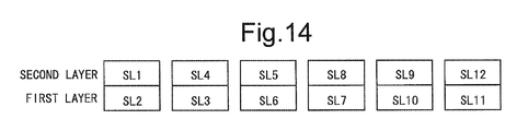
- FIG. 14 is a cross-sectional view taken along line A 2 -A 2 in FIG. 13 .
- FIG. 15 is a circuit diagram illustrating a detailed configuration of the testing circuit according to a fourth variant of the first embodiment.
- FIG. 16 is a diagram for illustration of a position of the testing circuit according to the first embodiment.
- FIG. 17 is a diagram for illustration of a position of the testing circuit according to the variant of the first embodiment.
- FIG. 18 is a diagram for illustration of a position of the testing circuit according to the variant of the first embodiment.
- FIG. 19 is a block diagram illustrating an entire configuration of an active matrix-type liquid crystal display device according to a second embodiment of the present invention.
- FIG. 20 is a circuit diagram illustrating a detailed configuration of a charge elimination circuit according to the second embodiment.
- FIG. 21 is a circuit diagram illustrating a detailed configuration of a charge elimination circuit according to a variant of the second embodiment.
- FIG. 22 is a diagram illustrating a wiring structure in a fan shape between an active area and external connecting terminals according to the conventional technique.
- FIG. 23 is a plan view illustrating one example of a conventional layered wiring structure.
- FIG. 24 is a diagram for detailed description of the wiring structure shown in FIG. 23 .
- FIG. 25 is a diagram for description of leakage of a first type to a third type according to the conventional technique.
- FIG. 26 is a cross-sectional view (schematic view) taken along line B-B in FIG. 23 .
- FIG. 27 is a diagram for illustration of a case in which a display device having the conventional layered wiring structure is provided with a simple testing circuit having two testing lines.
- FIG. 28 is a diagram for illustration of a case in which a display device having the conventional layered wiring structure is provided with a simple testing circuit having two testing lines.
- FIG. 29 is a diagram for illustration of a case in which a display device having the conventional layered wiring structure is provided with a simple testing circuit having two testing lines.
- FIG. 2 is a block diagram illustrating an entire configuration of an active matrix-type liquid crystal display device according to a first embodiment of the present invention.
- this liquid crystal display device is provided with a source driver 20 , a gate driver 30 , a testing circuit 60 , and an active area (display region) 40 .
- the active area 40 , the gate driver 30 , and the testing circuit 60 are provided on a panel substrate 10 .
- the panel substrate 10 in this embodiment is a glass substrate.
- the source driver 20 is mounted on the panel substrate 10 in a COG (Chip On Glass) manner, for example.
- the source driver 20 in this embodiment is an IC chip.
- a region indicated by a reference character 50 in FIG. 2 is a layered region (a region having a layered wiring structure). As illustrated in FIG. 3 , the layered region 50 is provided between external connecting terminals 15 and the testing circuit 60 .
- the wiring structure of the layered region 50 will be described in detail later.
- the testing circuit 60 examines whether or not there is leakage between adjacent source bus lines SL. A detailed description of the testing circuit 60 will be given later.
- a plurality of source bus lines SL and a plurality of gate bus lines GL are provided in the active area 40 .
- a pixel formation portion constituting a pixel (not shown in FIG. 2 ) is provided correspondingly at each of intersections between the plurality of source bus lines SL and the plurality of gate bus lines GL.
- the active area 40 is provided with a plurality of pixel formation portions.
- FIG. 4 is a diagram illustrating a configuration of a pixel formation portion 4 .
- the pixel formation portion 4 includes a TFT (Thin-Film Transistor) 49 as a switching element in which a gate bus line GL passing a corresponding intersection is connected to a gate terminal and a source bus line SL passing the same intersection is connected to a source terminal, a pixel electrode 41 connected to a drain terminal of the TFT 49 , a common electrode 44 and an auxiliary capacitance electrode 45 commonly provided for the plurality of pixel formation portions 4 , a liquid crystal capacitance 42 constituted by the pixel electrode 41 and the common electrode 44 , and an auxiliary capacitance 43 constituted by the pixel electrode 41 and the auxiliary capacitance electrode 45 .
- the liquid crystal capacitance 42 and the auxiliary capacitance 43 constitute a pixel capacitance 46 .
- an oxide TFT (a thin-film transistor in which an oxide semiconductor is used for a channel layer) may be employed, for example.
- the oxide TFT include TFTs containing InGaZnO (Indium Gallium Zinc Oxide).
- the oxide TFT is characterized by high mobility and low leakage current. Therefore, employing an oxide TFT provides effects of downsizing and reduced power consumption.
- the present invention is not limited to such an example. For example, it is possible to employ a TFT in which amorphous silicon is used for a channel layer.
- a display controller for controlling an operation of the source driver 20 and the gate driver 30 is provided outside the panel substrate (e.g., on a flexible substrate connected to the panel substrate 10 ).
- a digital video signal and a source control signal are transmitted to the source driver 20 from the display controller, and a gate control signal is transmitted to the gate driver 30 from the display controller.
- the source control signal includes, for example, a source start pulse signal, a source clock signal, and a latch strobe signal.
- the gate control signal includes, for example, a gate start pulse signal and a gate clock signal.
- the source driver 20 receives the digital video signal and the source control signal transmitted from the display controller, and applies a video signal for driving to each of the source bus lines SL.
- the source driver 20 sequentially holds digital video signals indicating voltages to be applied to the respective source bus lines SL at timing at which a pulse of the source clock signal is generated.
- the held digital video signals are converted into analog voltages.
- the converted analog voltages are applied as the video signals for driving to all the source bus lines SL at once.
- the gate driver 30 repeats application of an active scanning signal to each of the gate bus lines GL with one vertical scanning period taken as a cycle, based on the gate control signal transmitted from the display controller.
- a desired image is displayed on the active area 40 serving as a display region.
- FIG. 1 is a plan view illustrating the wiring structure of the layered region 50 according to this embodiment.
- the wiring structure is configured by first-layer wiring lines K 1 provided in a first layer (a lower layer in this case) and second-layer wiring lines K 2 provided in a second layer (an upper layer in this case).
- the first-layer wiring lines K 1 and the second-layer wiring lines K 2 are connected by contacts CT, respectively.
- the source bus lines SL 1 to SL 4 of the first column to the fourth column are focused on in FIG. 1 .
- the source bus line SL 1 of the first column and the source bus line SL 4 of the fourth column are configured only by the first-layer wiring lines K 1
- the source bus line SL 2 of the second column and the source bus line SL 3 of the third column are configured by the first-layer wiring lines K 1 and the second-layer wiring lines K 2 .
- this configuration is repeatedly provided every four columns.
- each of source bus lines SL of (4n ⁇ 3)th columns and source bus lines SL of 4n-th columns is configured only by the first-layer wiring line K 1
- each of source bus lines SL of (4n ⁇ 2)th columns and source bus lines SL of (4n ⁇ 1)th columns is configured by the first-layer wiring line K 1 and the second-layer wiring line K 2 .
- FIG. 5 is a cross-sectional view (schematic view) taken along line A-A in FIG. 1 .
- the source bus lines SL of the (4n ⁇ 3)th columns and the source bus lines SL of the 4n-th columns are provided in the first layer, and the source bus lines SL of the (4n ⁇ 2)th columns and the source bus lines SL of the (4n ⁇ 1)th columns are provided in the second layer.
- FIG. 6 is a circuit diagram illustrating a detailed configuration of the testing circuit 60 according to this embodiment.
- the testing circuit 60 includes two testing lines (a first testing line TL 1 and a second testing line TL 2 ), a single control line CL, and testing switches T_SW respectively provided for the source bus lines SL.
- a first potential TV 1 is supplied to the first testing line TL 1 .
- a second potential TV 2 is supplied to the second testing line TL 2 .
- the magnitude of the first potential TV 1 and the magnitude of the second potential TV 2 are different.
- Each of the testing switches T_SW is configured by a TFT.
- a gate electrode is connected to the control line CL
- a drain electrode is connected to either of the first testing line TL 1 and the second testing line TL 2
- a source electrode is connected to the source bus line SL.
- the control line CL is supplied with a control signal for turning the testing switches T_SW on when an examination is carried out.
- a first-type potential supply line is implemented by the first testing line TL 1
- a second-type potential supply line is implemented by the second testing line TL 2 .
- the drain electrodes of the testing switches T_SW provided respectively for the source bus lines SL of the odd-numbered columns are all connected to the first testing line TL 1 . Further, the drain electrodes of the testing switches T_SW provided respectively for the source bus lines SL of the even-numbered columns are all connected to the second testing line TL 2 .
- liquid crystal display device having a layered wiring structure
- leakage short circuit
- Second type leakage occurred between two adjacent source bus lines SL in a non-layered region.
- Second type leakage occurred between two adjacent source bus lines SL in the vertical direction in the layered region 50 .
- Third type leakage occurred between two adjacent source bus lines SL in the horizontal direction in the layered region 50 .
- a portion indicated by a reference character 76 in FIG. 7 schematically shows leakage of the first type
- a portion indicated by a reference character 77 in FIG. 7 schematically shows leakage of the second type
- a portion indicated by a reference character 78 in FIG. 7 schematically shows leakage of the third type.
- the source bus line SL 6 of the sixth column is focused on.
- Examples of leakage occurred between the source bus line SL 6 of the sixth column and another source bus lines SL include the following.
- Second type leakage between the source bus line SL 6 of the sixth column and the source bus line SL 5 of the fifth column, and leakage between the source bus line SL 6 of the sixth column and the source bus line SL 7 of the seventh column (see FIG. 1 ).
- Second type leakage between the source bus line SL 6 of the sixth column and the source bus line SL 5 of the fifth column (see FIG. 5 ).
- Third type leakage between the source bus line SL 6 of the sixth column and the source bus line SL 3 of the third column, and leakage between the source bus line SL 6 of the sixth column and the source bus line SL 7 of the seventh column (see FIG. 5 ).
- the second potential TV 2 is supplied as a testing potential to the source bus line SL 6 of the sixth column
- the first potential TV 1 is supplied as a testing potential to the source bus lines SL 3 , SL 5 , and SL 7 of the third column, the fifth column, and the seventh column. Therefore, it is possible to detect leakage between the source bus line SL 6 of the sixth column and the source bus line SL 3 of the third column (see a heavy dashed line indicated by a reference character 71 in FIG. 6 ), leakage between the source bus line SL 6 of the sixth column and the source bus line SL 5 of the fifth column (see a heavy dashed line indicated by a reference character 72 in FIG.
- leakage between the source bus line SL 6 of the sixth column and the source bus line SL 7 of the seventh column see a heavy dashed line indicated by a reference character 73 in FIG. 6 ). Specifically, leakage of any of the first type, the second type, and the third type can be detected.
- two source bus lines SL adjacent in the vertical direction in the layered region 50 are a combination of a source bus line SL of an odd-numbered column and a source bus line SL of an even-numbered column
- two source bus lines SL adjacent in the horizontal direction in the layered region 50 are a combination of a source bus line SL of an odd-numbered column and a source bus line SL of an even-numbered column. Because such a wiring structure is employed, by supplying testing potentials of different magnitudes to the source bus lines SL of the odd-numbered columns and the source bus lines SL of the even-numbered columns using the two testing lines as illustrated in FIG.
- the testing potentials of different magnitudes are supplied to any two adjacent source bus lines SL in the non-layered region, the testing potentials of different magnitudes are supplied to any two source bus lines SL adjacent in the vertical direction in the layered region 50 , and the testing potentials of different magnitudes are supplied to any two source bus lines SL adjacent in the horizontal direction in the layered region 50 .
- a display device having a layered wiring structure is realized, that is capable of detecting leakage without fail by using a simple testing circuit.
- the present invention is not limited to such an example.
- the present invention may also be applied to a case in which the number of the layers of wiring is three or more. Therefore, in the following, an example in which the number of the layers of wiring is three will be described as a first variant, and an example in which the number of the layers of wiring is four will be described as a second variant.
- FIG. 8 is a schematic cross-sectional view illustrating one example of the wiring structure according to this variant.
- two source bus lines SL adjacent in the vertical direction are a combination of a source bus line SL of an odd-numbered column and a source bus line SL of an even-numbered column
- two source bus lines SL adjacent in the horizontal direction are a combination of a source bus line SL of an odd-numbered column and a source bus line SL of an even-numbered column.
- a consideration is given on provision of the testing circuit 60 having a configuration illustrated in FIG. 6 for a liquid crystal display device having a wiring structure as illustrated in FIG. 8 .
- testing potentials of different magnitudes are supplied respectively to the source bus lines SL of the odd-numbered columns and the source bus lines SL of the even-numbered columns. Then, as can be seen from FIG. 8 , testing potentials of different magnitudes are supplied respectively to any two source bus lines SL adjacent in the vertical direction in the layered region 50 , and testing potentials of different magnitudes are also supplied respectively to any two source bus lines SL adjacent in the horizontal direction in the layered region 50 . Further, testing potentials of different magnitudes are supplied respectively to any two adjacent source bus lines SL in the non-layered region.
- a display device having a layered wiring structure is realized, that is capable of detecting leakage without fail by using a simple testing circuit.
- FIG. 9 is a schematic cross-sectional view illustrating another example of the wiring structure according to this variant.
- two source bus lines SL adjacent in the vertical direction are a combination of a source bus line SL of an odd-numbered column and a source bus line SL of an even-numbered column
- two source bus lines SL adjacent in the horizontal direction are a combination of a source bus line SL of an odd-numbered column and a source bus line SL of an even-numbered column.
- testing potentials of different magnitudes are supplied respectively to any two source bus lines SL adjacent in the vertical direction in the layered region 50 , and testing potentials of different magnitudes are also supplied respectively to any two source bus lines SL adjacent in the horizontal direction in the layered region 50 . Further, testing potentials of different magnitudes are also supplied respectively to any two adjacent source bus lines SL in the non-layered region. Therefore, also in this variant, it is possible to detect leakage of any of patterns described above without fail by using the testing circuit 60 having only two testing lines. Specifically, also in this variant, a display device having a layered wiring structure is realized, that is capable of detecting leakage without fail by using a simple testing circuit.
- FIG. 10 is a schematic cross-sectional view illustrating one example of the wiring structure according to this variant.
- FIG. 11 is a schematic cross-sectional view illustrating another example of the wiring structure according to this variant.
- FIG. 12 is a schematic cross-sectional view illustrating still another example of the wiring structure according to this variant.
- two source bus lines SL adjacent in the vertical direction are a combination of a source bus line SL of an odd-numbered column and a source bus line SL of an even-numbered column
- two source bus lines SL adjacent in the horizontal direction are a combination of a source bus line SL of an odd-numbered column and a source bus line SL of an even-numbered column.
- a display device having a layered wiring structure is realized, that is capable of detecting leakage without fail by using a simple testing circuit.
- the panel substrate 10 is provided with only one layered region 50 in the first embodiment, the present invention is not limited to such an example. Then, in the following, an example in which the panel substrate 10 is provided with two layered regions 50 will be described as a third variant.
- FIG. 13 is a plan view illustrating a wiring structure (a wiring structure between the external connecting terminals 15 and the active area 40 ) of the layered region 50 according to this variant.
- the liquid crystal display device according to this variant is provided with two layered regions (a first layered region 50 a and a second layered region 50 b ).
- a cross-sectional view of the first layered region 50 a (a cross-sectional view taken along line A 1 -A 1 in FIG. 13 ) is as shown in FIG. 5 .
- a cross-sectional view of the second layered region 50 b (a cross-sectional view taken along line A 2 -A 2 in FIG. 13 ) is as shown in FIG. 14 .
- FIG. 13 FIG.
- the source bus lines SL provided in the first layer in the first layered region 50 a are provided in the second layer in the second layered region 50 b
- the source bus lines SL provided in the second layer in the first layered region 50 a are provided in the first layer in the second layered region 50 b.
- the source bus lines SL of a half of an entire lines are configured only by the first-layer wiring lines K 1 , and the remaining half of the source bus lines SL are configured by the first-layer wiring lines K 1 and the second-layer wiring lines K 2 .
- all of the source bus lines SL are configured by the first-layer wiring lines K 1 and the second-layer wiring lines K 2 . It should be noted that, regarding all of the source bus lines SL, the first-layer wiring lines K 1 and the second-layer wiring lines K 2 are respectively connected by the contacts CT at a boundary portion between the first layered region 50 a and the second layered region 50 b.
- two source bus lines SL adjacent in the vertical direction are a combination of a source bus line SL of an odd-numbered column and a source bus line SL of an even-numbered column
- two source bus lines SL adjacent in the horizontal direction are a combination of a source bus line SL of an odd-numbered column and a source bus line SL of an even-numbered column. Therefore, also in the case in which the two layered regions 50 are disposed on the panel substrate 10 , it is possible to detect leakage without fail by using a simple testing circuit.
- testing circuit 60 includes only two testing lines in the first embodiment, the present invention is not limited to such an example.
- the testing circuit 60 may include three or more testing lines. Then, in the following, an example in which the testing circuit 60 includes four testing lines will be described as a fourth variant.
- FIG. 15 is a circuit diagram illustrating a detailed configuration of the testing circuit 60 according to this variant.
- the testing circuit 60 includes four testing lines (first to fourth testing lines TL 1 to TL 4 ).
- a testing potential is supplied from the first testing line TL 1 to the source bus lines SL of the (4n ⁇ 3)th columns
- a testing potential is supplied from the second testing line TL 2 to the source bus lines SL of the (4n ⁇ 2)th columns
- a testing potential is supplied from the third testing line TL 3 to the source bus lines SL of the (4n ⁇ 1)th columns
- a testing potential is supplied from the fourth testing line TL 4 to the source bus lines SL of the 4n-th columns.
- the first potential TV 1 is supplied as a testing potential to the first testing line TL 1 and the third testing line TL 3
- the second potential TV 2 is supplied as a testing potential to the second testing line TL 2 and the fourth testing line TL 4 . Therefore, similarly to the first embodiment, testing potentials of different magnitudes are supplied respectively to the source bus lines SL of the odd-numbered columns and the source bus lines SL of the even-numbered columns. As described above, the number of the testing lines included in the testing circuit 60 may be three or more.
- the first-type potential supply line is implemented by the first testing line TL 1 and the third testing line TL 3
- the second-type potential supply line is implemented by the second testing line TL 2 and the fourth testing line TL 4 .
- the testing circuit 60 is provided in the region between the layered region 50 and the active area 40 (see FIG. 16 ).
- a position at which the testing circuit 60 is provided is not particularly limited. As illustrated in FIG. 17 , for example, it is possible to employ a configuration in which the testing circuit 60 is provided in a region on an opposite side of the layered region 50 with respect to the active area 40 . Further, as illustrated in FIG. 18 , for example, it is possible to employ a configuration in which the testing circuit 60 is disposed under the source driver 20 (IC chip).
- FIG. 19 is a block diagram illustrating an entire configuration of the active matrix-type liquid crystal display device according to a second embodiment of the present invention.
- the liquid crystal display device according to this embodiment is provided with a charge elimination circuit 70 in place of the testing circuit 60 in the first embodiment.
- the charge elimination circuit 70 is provided in a region between the active area 40 and the layered region 50 .
- the charge elimination circuit 70 eliminates electric charges from the source bus lines SL and the pixel formation portions 4 when a device is turned off or terminated abnormally.
- the components other than the charge elimination circuit 70 are the same as those of the first embodiment, and therefore a description for these components will be omitted.
- the wiring structure of the layered region 50 is the same as that of the first embodiment (see FIG. 1 and FIG. 5 ).
- FIG. 20 is a circuit diagram illustrating a detailed configuration of the charge elimination circuit 70 according to this embodiment.
- the charge elimination circuit 70 includes a single reference potential line BL, a single control line CL, and control switches C_SW provided for the source bus lines SL.
- a ground potential GND is supplied to the reference potential line BL.
- Each of the control switches C_SW is configured by a TFT.
- a gate electrode is connected to the control line CL
- a drain electrode is connected to the reference potential line BL
- a source electrode is connected to the source bus line SL.
- this embodiment it is possible to supply the ground potential GND to all of the source bus lines SL when a device is turned off or terminated abnormally, for example. Therefore, electric charges on the source bus lines SL can be eliminated as needed. With this, it is possible to suppress deterioration of display quality due to presence of a residual electric charge in a display device having a layered wiring structure.
- the charge elimination circuit 70 includes only one reference potential line in the second embodiment, the present invention is not limited to such an example, and the charge elimination circuit 70 may include a plurality of reference potential lines.
- the charge elimination circuit 70 may include two reference potential lines (a first reference potential line BL 1 and a second reference potential line BL 2 ) as illustrated in FIG. 21 is employed, and the ground potential GND may be supplied to these two reference potential lines.
- the present invention is not limited to the embodiments described above, and various modifications may be made without departing from the scope of the present invention.
- the description is given taking the liquid crystal display device as an example in the above embodiments, the present invention is not limited to such an example.
- the present invention may be applied to a display device other than the liquid crystal display device, such as an organic EL (Electro Luminescence) display device.
Landscapes
- Physics & Mathematics (AREA)
- Engineering & Computer Science (AREA)
- General Physics & Mathematics (AREA)
- Theoretical Computer Science (AREA)
- Computer Hardware Design (AREA)
- Chemical & Material Sciences (AREA)
- Crystallography & Structural Chemistry (AREA)
- Nonlinear Science (AREA)
- Optics & Photonics (AREA)
- Mathematical Physics (AREA)
- Liquid Crystal (AREA)
- Devices For Indicating Variable Information By Combining Individual Elements (AREA)
- Liquid Crystal Display Device Control (AREA)
Applications Claiming Priority (3)
| Application Number | Priority Date | Filing Date | Title |
|---|---|---|---|
| JP2014-236425 | 2014-11-21 | ||
| JP2014236425 | 2014-11-21 | ||
| PCT/JP2015/081925 WO2016080291A1 (ja) | 2014-11-21 | 2015-11-13 | 表示装置 |
Publications (2)
| Publication Number | Publication Date |
|---|---|
| US20170336667A1 US20170336667A1 (en) | 2017-11-23 |
| US10241369B2 true US10241369B2 (en) | 2019-03-26 |
Family
ID=56013832
Family Applications (1)
| Application Number | Title | Priority Date | Filing Date |
|---|---|---|---|
| US15/520,271 Active 2035-12-28 US10241369B2 (en) | 2014-11-21 | 2015-11-13 | Display device |
Country Status (4)
| Country | Link |
|---|---|
| US (1) | US10241369B2 (ja) |
| JP (1) | JP6403796B2 (ja) |
| CN (1) | CN107004386B (ja) |
| WO (1) | WO2016080291A1 (ja) |
Cited By (1)
| Publication number | Priority date | Publication date | Assignee | Title |
|---|---|---|---|---|
| US11329071B2 (en) | 2017-01-31 | 2022-05-10 | Semiconductor Energy Laboratory Co., Ltd. | Display device, display module, and electronic device |
Families Citing this family (3)
| Publication number | Priority date | Publication date | Assignee | Title |
|---|---|---|---|---|
| CN110720117B (zh) * | 2017-06-02 | 2021-10-12 | 夏普株式会社 | 显示装置 |
| JP7246534B2 (ja) * | 2017-11-22 | 2023-03-27 | 株式会社ジャパンディスプレイ | アレイ基板 |
| JP7028616B2 (ja) * | 2017-11-22 | 2022-03-02 | 株式会社ジャパンディスプレイ | 表示装置 |
Citations (11)
| Publication number | Priority date | Publication date | Assignee | Title |
|---|---|---|---|---|
| JPH0519282A (ja) | 1991-07-16 | 1993-01-29 | Nec Corp | 液晶表示装置及び液晶表示パネル |
| US20080001892A1 (en) * | 2006-06-30 | 2008-01-03 | Samsung Electronics Co., Ltd. | Display substrate and display device having the same |
| US20080179593A1 (en) * | 2007-01-25 | 2008-07-31 | Ji-Suk Lim | Thin film transistor array panel and method of manufacturing the same |
| US20080203391A1 (en) * | 2007-02-28 | 2008-08-28 | Samsung Electronics Co., Ltd. | Array substrate, display apparatus having the same |
| US20080284697A1 (en) * | 2006-09-25 | 2008-11-20 | Nam Young-Joo | Display apparatus |
| US20090096975A1 (en) * | 2007-10-16 | 2009-04-16 | Kwon Jang-Un | Liquid crystal display device and method of manufacturing the same |
| US20110063534A1 (en) * | 2009-09-15 | 2011-03-17 | Cho Suk-Ho | Liquid crystal display device and method of fabricating the same |
| US20140284574A1 (en) * | 2013-03-20 | 2014-09-25 | Samsung Display Co., Ltd. | Display apparatus and method of manufacturing the same |
| US20150325159A1 (en) * | 2013-08-29 | 2015-11-12 | Beijing Boe Display Technology Co., Ltd. | Array substrate and testing method and manufacturing method thereof |
| US20160026053A1 (en) * | 2013-04-08 | 2016-01-28 | Panasonic Liquid Crystal Display Co., Ltd. | Display device |
| US20170336688A1 (en) * | 2014-11-21 | 2017-11-23 | Sharp Kabushiki Kaisha | Display device |
Family Cites Families (8)
| Publication number | Priority date | Publication date | Assignee | Title |
|---|---|---|---|---|
| JP3667548B2 (ja) * | 1998-03-27 | 2005-07-06 | シャープ株式会社 | アクティブマトリクス型液晶表示パネル及びその検査方法 |
| JP4006284B2 (ja) * | 2002-07-17 | 2007-11-14 | 株式会社 日立ディスプレイズ | 液晶表示装置 |
| WO2007063620A1 (ja) * | 2005-11-30 | 2007-06-07 | Sharp Kabushiki Kaisha | 表示装置および表示部材の駆動方法 |
| CN101999095B (zh) * | 2008-05-16 | 2012-05-09 | 夏普株式会社 | 有源矩阵基板、显示装置、有源矩阵基板的检查方法和显示装置的检查方法 |
| WO2011007591A1 (ja) * | 2009-07-15 | 2011-01-20 | シャープ株式会社 | 走査信号線駆動回路およびそれを備えた表示装置 |
| US9177517B2 (en) * | 2012-02-10 | 2015-11-03 | Sharp Kabushiki Kaisha | Display device and drive method therefor |
| US9536905B2 (en) * | 2012-11-08 | 2017-01-03 | Sharp Kabushiki Kaisha | Active matrix substrate and display device using same |
| CN103926766B (zh) * | 2013-08-07 | 2016-10-12 | 上海中航光电子有限公司 | 像素阵列及液晶显示装置 |
-
2015
- 2015-11-13 JP JP2016560179A patent/JP6403796B2/ja active Active
- 2015-11-13 CN CN201580062616.4A patent/CN107004386B/zh active Active
- 2015-11-13 US US15/520,271 patent/US10241369B2/en active Active
- 2015-11-13 WO PCT/JP2015/081925 patent/WO2016080291A1/ja active Application Filing
Patent Citations (11)
| Publication number | Priority date | Publication date | Assignee | Title |
|---|---|---|---|---|
| JPH0519282A (ja) | 1991-07-16 | 1993-01-29 | Nec Corp | 液晶表示装置及び液晶表示パネル |
| US20080001892A1 (en) * | 2006-06-30 | 2008-01-03 | Samsung Electronics Co., Ltd. | Display substrate and display device having the same |
| US20080284697A1 (en) * | 2006-09-25 | 2008-11-20 | Nam Young-Joo | Display apparatus |
| US20080179593A1 (en) * | 2007-01-25 | 2008-07-31 | Ji-Suk Lim | Thin film transistor array panel and method of manufacturing the same |
| US20080203391A1 (en) * | 2007-02-28 | 2008-08-28 | Samsung Electronics Co., Ltd. | Array substrate, display apparatus having the same |
| US20090096975A1 (en) * | 2007-10-16 | 2009-04-16 | Kwon Jang-Un | Liquid crystal display device and method of manufacturing the same |
| US20110063534A1 (en) * | 2009-09-15 | 2011-03-17 | Cho Suk-Ho | Liquid crystal display device and method of fabricating the same |
| US20140284574A1 (en) * | 2013-03-20 | 2014-09-25 | Samsung Display Co., Ltd. | Display apparatus and method of manufacturing the same |
| US20160026053A1 (en) * | 2013-04-08 | 2016-01-28 | Panasonic Liquid Crystal Display Co., Ltd. | Display device |
| US20150325159A1 (en) * | 2013-08-29 | 2015-11-12 | Beijing Boe Display Technology Co., Ltd. | Array substrate and testing method and manufacturing method thereof |
| US20170336688A1 (en) * | 2014-11-21 | 2017-11-23 | Sharp Kabushiki Kaisha | Display device |
Cited By (2)
| Publication number | Priority date | Publication date | Assignee | Title |
|---|---|---|---|---|
| US11329071B2 (en) | 2017-01-31 | 2022-05-10 | Semiconductor Energy Laboratory Co., Ltd. | Display device, display module, and electronic device |
| US11515340B2 (en) * | 2017-01-31 | 2022-11-29 | Semiconductor Energy Laboratory Co., Ltd. | Display device, display module, and electronic device |
Also Published As
| Publication number | Publication date |
|---|---|
| WO2016080291A1 (ja) | 2016-05-26 |
| CN107004386B (zh) | 2019-10-15 |
| CN107004386A (zh) | 2017-08-01 |
| US20170336667A1 (en) | 2017-11-23 |
| JP6403796B2 (ja) | 2018-10-10 |
| JPWO2016080291A1 (ja) | 2017-07-27 |
Similar Documents
| Publication | Publication Date | Title |
|---|---|---|
| US10228595B2 (en) | Display device with layered wiring structure for external connection | |
| US8791883B2 (en) | Organic EL display device and control method thereof | |
| US9685127B2 (en) | Array substrate, method for driving array substrate, and display device | |
| US9552771B2 (en) | Display apparatus and method of controlling the same | |
| US20140078123A1 (en) | Display panel | |
| KR101635670B1 (ko) | 표시 장치 | |
| US10241369B2 (en) | Display device | |
| US10199004B2 (en) | Display device | |
| KR20160027558A (ko) | 표시 장치 | |
| US10896639B2 (en) | Display apparatus and driving method thereof | |
| US20070040568A1 (en) | Semiconductor device, driving method and inspection method thereof | |
| US7612752B2 (en) | Flat panel display and pixel driving method applied thereto | |
| US20110063260A1 (en) | Driving circuit for liquid crystal display | |
| US8896635B2 (en) | Display device | |
| JP2005202254A (ja) | 表示装置 | |
| US8994635B2 (en) | Display device | |
| US11823636B2 (en) | Array substrate, display device and driving method thereof | |
| US11295658B2 (en) | Display panel and display device | |
| JP2007010900A (ja) | 液晶表示装置 | |
| KR20040063521A (ko) | 박막 트랜지스터 표시판 및 이를 포함하는 액정 표시 장치 | |
| JP2005181777A (ja) | 表示装置及びその駆動方法 |
Legal Events
| Date | Code | Title | Description |
|---|---|---|---|
| AS | Assignment |
Owner name: SHARP KABUSHIKI KAISHA, JAPAN Free format text: ASSIGNMENT OF ASSIGNORS INTEREST;ASSIGNORS:YAMAMOTO, ETSUO;OHKAWA, HIROYUKI;FURUTA, SHIGE;REEL/FRAME:042063/0987 Effective date: 20170411 |
|
| STCF | Information on status: patent grant |
Free format text: PATENTED CASE |
|
| MAFP | Maintenance fee payment |
Free format text: PAYMENT OF MAINTENANCE FEE, 4TH YEAR, LARGE ENTITY (ORIGINAL EVENT CODE: M1551); ENTITY STATUS OF PATENT OWNER: LARGE ENTITY Year of fee payment: 4 |