US10205487B1 - Wireless power consortium device and method for manufacturing the same - Google Patents
Wireless power consortium device and method for manufacturing the same Download PDFInfo
- Publication number
- US10205487B1 US10205487B1 US15/870,882 US201815870882A US10205487B1 US 10205487 B1 US10205487 B1 US 10205487B1 US 201815870882 A US201815870882 A US 201815870882A US 10205487 B1 US10205487 B1 US 10205487B1
- Authority
- US
- United States
- Prior art keywords
- coil
- wpc
- nfc
- copper layer
- matching circuit
- Prior art date
- Legal status (The legal status is an assumption and is not a legal conclusion. Google has not performed a legal analysis and makes no representation as to the accuracy of the status listed.)
- Active
Links
- 238000000034 method Methods 0.000 title claims description 22
- 238000004519 manufacturing process Methods 0.000 title claims description 6
- 239000000758 substrate Substances 0.000 claims abstract description 42
- RYGMFSIKBFXOCR-UHFFFAOYSA-N Copper Chemical compound [Cu] RYGMFSIKBFXOCR-UHFFFAOYSA-N 0.000 claims description 82
- 229910052802 copper Inorganic materials 0.000 claims description 82
- 239000010949 copper Substances 0.000 claims description 82
- 238000004891 communication Methods 0.000 claims description 2
- 238000005530 etching Methods 0.000 claims description 2
- 230000003014 reinforcing effect Effects 0.000 description 13
- PCHJSUWPFVWCPO-UHFFFAOYSA-N gold Chemical compound [Au] PCHJSUWPFVWCPO-UHFFFAOYSA-N 0.000 description 11
- 229910052737 gold Inorganic materials 0.000 description 11
- 239000010931 gold Substances 0.000 description 11
- 229920000106 Liquid crystal polymer Polymers 0.000 description 4
- 239000004977 Liquid-crystal polymers (LCPs) Substances 0.000 description 4
- 239000004698 Polyethylene Substances 0.000 description 4
- 239000004642 Polyimide Substances 0.000 description 4
- 229920000573 polyethylene Polymers 0.000 description 4
- -1 polyethylene terephthalate Polymers 0.000 description 4
- 229920000139 polyethylene terephthalate Polymers 0.000 description 4
- 239000005020 polyethylene terephthalate Substances 0.000 description 4
- 229920001721 polyimide Polymers 0.000 description 4
- 229920000915 polyvinyl chloride Polymers 0.000 description 4
- 239000004800 polyvinyl chloride Substances 0.000 description 4
- 238000005553 drilling Methods 0.000 description 3
- 238000007747 plating Methods 0.000 description 3
- 239000004809 Teflon Substances 0.000 description 2
- 229920006362 Teflon® Polymers 0.000 description 2
- 238000011156 evaluation Methods 0.000 description 2
- 239000000463 material Substances 0.000 description 2
- 239000011112 polyethylene naphthalate Substances 0.000 description 2
- 229920000642 polymer Polymers 0.000 description 2
- 230000008859 change Effects 0.000 description 1
- 230000001627 detrimental effect Effects 0.000 description 1
- 230000006872 improvement Effects 0.000 description 1
- 230000008569 process Effects 0.000 description 1
Images


Classifications
-
- H—ELECTRICITY
- H04—ELECTRIC COMMUNICATION TECHNIQUE
- H04B—TRANSMISSION
- H04B5/00—Near-field transmission systems, e.g. inductive or capacitive transmission systems
- H04B5/70—Near-field transmission systems, e.g. inductive or capacitive transmission systems specially adapted for specific purposes
- H04B5/79—Near-field transmission systems, e.g. inductive or capacitive transmission systems specially adapted for specific purposes for data transfer in combination with power transfer
-
- H04B5/0037—
-
- H—ELECTRICITY
- H01—ELECTRIC ELEMENTS
- H01F—MAGNETS; INDUCTANCES; TRANSFORMERS; SELECTION OF MATERIALS FOR THEIR MAGNETIC PROPERTIES
- H01F27/00—Details of transformers or inductances, in general
- H01F27/28—Coils; Windings; Conductive connections
- H01F27/2804—Printed windings
-
- H—ELECTRICITY
- H01—ELECTRIC ELEMENTS
- H01F—MAGNETS; INDUCTANCES; TRANSFORMERS; SELECTION OF MATERIALS FOR THEIR MAGNETIC PROPERTIES
- H01F38/00—Adaptations of transformers or inductances for specific applications or functions
- H01F38/14—Inductive couplings
-
- H—ELECTRICITY
- H02—GENERATION; CONVERSION OR DISTRIBUTION OF ELECTRIC POWER
- H02J—CIRCUIT ARRANGEMENTS OR SYSTEMS FOR SUPPLYING OR DISTRIBUTING ELECTRIC POWER; SYSTEMS FOR STORING ELECTRIC ENERGY
- H02J50/00—Circuit arrangements or systems for wireless supply or distribution of electric power
- H02J50/20—Circuit arrangements or systems for wireless supply or distribution of electric power using microwaves or radio frequency waves
Definitions
- the subject matter generally relates to a wireless power consortium device and method for manufacturing the same.
- the near field communication (NFC) coil and the wireless power consortium (WPC) coil are generally set in the case back cover. But the thickness of the product is increased and does not meet the thinness trend of electronic products.
- high-end electronic products such as high-end mobile phones that integrate the NFC coils and the WPC coils with flexible substrates.
- important chips are still installed on the motherboard, which is detrimental to evaluation and debugging, and takes a long time to develop. Improvement in the art is preferred.
- FIG. 1 is a top view of an exemplary embodiment of a wireless power consortium device of the present disclosure.
- FIG. 2 is a cross-sectional view taken along line II-II of FIG. 1 .
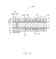
- FIG. 3 is a cross-sectional view taken along line of FIG. 1 .
- FIG. 4 is a flowchart of an exemplary embodiment of a method for manufacturing the wireless power consortium device of FIG. 1 .
- FIG. 5 is a cross-sectional view of a clad substrate according to the present disclosure.
- FIG. 6 is a cross-sectional view showing through holes in the double-sided copper clad substrate of FIG. 5 .
- FIG. 7 is a cross-sectional view showing plated copper layer formed on the clad substrate of FIG. 5 .
- FIG. 8 is a cross-sectional view showing the plated copper layer of FIG. 7 reduced.
- FIG. 9 is a cross-sectional view showing NFC coils, WPC coils and matching lines.
- FIG. 10 is a cross-sectional view showing covering layers formed on the NFC coils, the WPC coils and the matching line according to FIG. 8 .
- FIG. 11 is a cross-sectional view showing a first gold layer and a second layer are formed on the matching line of FIG. 9 .
- FIG. 12 is a cross-sectional view showing a reinforcing board formed on the back of the matching lines of FIG. 9 .
- FIGS. 1 to 3 illustrate an exemplary embodiment of a wireless power consortium device 100 .
- the wireless power consortium device 100 is used to receive an external radio frequency signal and to receive power for battery charging from external charging equipment.
- the wireless power consortium device 100 defines a WPC coil area 110 , an NFC coil area 120 , and a matching line area 130 .
- the NFC coil area 120 surrounds the WPC coil area 110 .
- the matching line area 130 surrounds the NFC coil area 120 .
- the wireless power consortium device 100 includes a flexible substrate layer 11 , at least one first WPC coil 21 , at least one first NFC coil 23 , at least one WPC module 25 , and at least one NFC module 26 .
- the flexible substrate layer 11 is a material selected from a group consisting of the polyimide (PI), polyethylene terephthalate (PET), polyethylene naphthalate (PEN), polyethylene (PE), Teflon, liquid crystal polymer (LCP), polyvinyl chloride polymer (PVC), and a combination thereof.
- PI polyimide
- PET polyethylene terephthalate
- PEN polyethylene naphthalate
- PE polyethylene
- Teflon polyethylene
- LCP liquid crystal polymer
- PVC polyvinyl chloride polymer
- the flexible substrate layer 11 includes a first surface 111 and a second surface 112 facing away from the first surface 111 .
- the at least one first WPC coil 21 , the at least one first NFC coil 23 , the at least one WPC module 25 , and the at least one NFC module 26 are all formed on the first surface 111 .
- the at least one first WPC coil 21 lies in the WPC coil area 110 .
- the at least one first NFC coil 23 lies in the NFC coil area 120 .
- the at least one WPC module 25 and the at least one NFC module 26 lie in the matching line area 130 .
- the at least one first NFC coil 23 surrounds the at least one first WPC coil 21 .
- the at least one WPC module 25 and the at least one NFC module 26 lie on outside of the at least one first NFC coil 23 .
- the WPC module 25 is adjacent to the NFC module 26 .
- a thickness of the at least one first WPC coil 21 is equal to or greater than 55 micrometers.
- a thickness of the at least one first NFC coil 23 is equal to or less than 35 micrometers.
- Each of the at least one WPC module 25 includes a first matching circuit 251 and a WPC power supply chip 252 .
- the WPC power supply chip 252 is electrically connected to the first matching circuit 251 .
- a thickness of the first matching circuit 251 is equal to or less than 18 micrometers.
- Each of the at least one NFC module 26 includes a second matching circuit 261 and an NFC controlling chip 262 .
- the NFC controlling chip 262 is electrically connected to the second matching circuit 261 .
- the first matching circuit 251 and the second matching circuit 261 are different parts of one circuit. That is, the first matching circuit 251 and the second matching circuit 261 are all formed on the first surface 111 and lie in the matching line area 130 . A thickness of the second matching circuit 261 is equal to or less than 18 micrometers.
- the wireless power consortium device 100 further includes at least one second WPC coil 22 , at least one second NFC coil 24 , and a third matching circuit 27 .
- the second WPC coil 22 , the second NFC coil 24 , and the third matching circuit 27 are formed on the second surface 112 .
- the second WPC coil 22 faces away from the first WPC coil 21 .
- the second NFC coil 24 faces away from the first NFC coil 23 .
- the third matching circuit 27 faces away from the first matching circuit 251 and the second matching circuit 261 .
- a thickness of the second WPC coil 22 is equal to a thickness of the first WPC coil 21 .
- a thickness of the second NFC coil 24 is equal to a thickness of the first NFC coil 23 .
- a thickness of the second WPC coil 22 is equal to or more than 55 micrometers.
- a thickness of the second NFC coil 24 is equal to or less than 35 micrometers.
- a thickness of the third matching circuit 27 is equal to or less than 18 micrometers.
- the wireless power consortium device 100 further includes at least one conductive through hole 17 .
- the conductive through hole 17 is electrically connected to the first matching circuit 251 , the second matching circuit 261 , and the third matching circuit 27 .
- the wireless power consortium device 100 further includes a first covering layer 28 and a second covering layer 29 .
- the first covering layer 28 covers the first WPC coil 21 , the first NFC coil 23 , the first matching circuit 251 , and the second matching circuit 261 .
- the second covering layer 29 covers the second WPC coil 22 , the second NFC coil 24 , and the third matching circuit 27 .
- the first covering layer 28 includes at least one first opening 281 and at least one second opening 282 .
- a portion of the first matching circuit 251 is exposed from the at least one first opening 281 , a portion of the second matching circuit 261 is exposed from the at least one second opening 282 .
- a first pad 2511 of the wireless power consortium device 100 defines the portion of the first matching circuit 251 which is exposed from the at least one first opening 281 .
- a second pad 2611 of the wireless power consortium device 100 defines the portion of the second matching circuit 261 exposed from the at least one second opening 282 .
- the second pad 2611 is used to mount the at least one NFC controlling chip 262 .
- a first gold layer 2512 is formed on the first pad 2511 .
- the first gold layer 2512 is used to protect the first pad 2511 .
- a second gold layer 2612 is formed on the second pad 2611 .
- the second gold layer 2612 is used to protect the second pad 2612 .
- the wireless power consortium device 100 further includes at least one first reinforcing board 30 and at least one second reinforcing board 40 .
- the at least one first reinforcing board 30 and the second reinforcing board 40 are formed on the second covering layer 29 and reinforce the flexible substrate 11 .
- the first reinforcing board 30 faces away from the first pad 2511 .
- the second reinforcing board 40 faces away from the second pad 2611 .
- the wireless power consortium device 100 does not include the second WPC coil 22 , the second NFC coil 24 , the third matching circuit 27 , and the second covering layer 29 .
- FIG. 4 illustrates a flowchart of a method for manufacturing a wireless power consortium device 100 .
- the method is provided by way of example, as there are a variety of ways to carry out the method. The method described below can be carried out using the configurations illustrated in FIGS. 1-3 , for example, and various elements of these figures are referenced in explaining example method.
- Each block shown in FIG. 4 represents one or more processes, methods, or subroutines, carried out in the exemplary method.
- the illustrated order of blocks is by example only and the order of the blocks can change. Additional blocks may be added or fewer blocks may be utilized, without departing from this disclosure.
- the exemplary method can begin at block 601 .
- a copper clad substrate 10 is provided.
- the copper clad substrate 10 can be a double-sided copper clad substrate or a single-sided copper clad substrate. In at least one exemplary embodiment, the copper clad substrate 10 is a double-sided copper clad substrate.
- the copper clad substrate 10 includes a flexible substrate layer 11 , a first copper layer 12 , and a second copper layer 13 .
- the flexible substrate layer 11 is a material selected from a group consisting of the polyimide (PI), polyethylene terephthalate (PET), polyethylene naphthalate (PEN), polyethylene (PE), Teflon, liquid crystal polymer (LCP), polyvinyl chloride polymer (PVC), and a combination thereof.
- PI polyimide
- PET polyethylene terephthalate
- PEN polyethylene naphthalate
- PE polyethylene
- Teflon polyethylene
- LCP liquid crystal polymer
- PVC polyvinyl chloride polymer
- the flexible substrate layer 11 includes a first surface 111 and a second surface 112 facing away from the first surface 111 .
- the first copper layer 12 is formed on the first surface 111 .
- the second copper layer 13 is formed on the second surface 112 .
- the copper clad substrate 10 defines a WPC coil area 110 , an NFC coil area 120 , and a matching line area 130 .
- the NFC coil area 120 surrounds the WPC coil area 110 .
- the matching line area 130 surrounds the NFC coil area 120 .
- the copper clad substrate 10 further includes at least one through hole 14 running through the copper clad substrate 10 .
- the at least one through hole 14 is formed by mechanical drilling or laser drilling. In at least one exemplary embodiment, the at least one through hole 14 is formed by mechanical drilling.
- a first plated copper layer 15 and a second plated copper layer 16 are formed on the copper clad substrate 10 .
- At least one conductive through hole 17 is formed by plating copper on inner surface of the at least one through hole 14 or infilling conductive paste in the at least one through hole 14 .
- the first plated copper layer 15 is formed on a surface of the first copper layer 12 facing away from the flexible substrate 11
- the second plated copper layer 16 is formed on a surface of the second copper layer 13 facing away from the flexible substrate 11 .
- the first plated copper layer 15 and the second plated copper layer 16 lie in the WPC coil area 110 .
- At block 603 also illustrated by FIGS. 8-9 , at least one first WPC coil 21 , at least one first NFC coil 23 , a first matching circuit 251 , a second matching circuit 261 , at least one second WPC coil 22 , at least one second NFC coil 24 , and a third matching circuit 27 are formed.
- the first copper layer 12 and the second copper layer 13 are locally reduced by etching.
- the first plated copper layer 15 and the second plated copper layer 16 lying in the WPC coil area 110 are not etched.
- the first copper layer 12 and the second copper layer 13 lying in the NFC coil area 120 are not etched.
- the first copper layer 12 and the second copper layer 13 lying in the matching line area 130 are locally etched.
- a sum of thicknesses of the first copper layer 12 and the first plated copper layer 15 lying in the WPC coil area 110 is equal to or greater than 55 micrometers.
- a sum of thicknesses of the second copper layer 13 and the second plated copper layer 16 lying in the WPC coil area 110 is equal to or greater than 55 micrometers.
- a thickness of the first copper layer 12 lying in the NFC coil area 120 is equal to or less than 35 micrometers.
- a thickness of the second copper layer 13 lying in the NFC coil area 120 is equal to or less than 35 micrometers.
- a thickness of the first copper layer 12 being etched and lying in the matching line area 130 is equal to or less than 18 micrometers.
- a thickness of the second copper layer 13 being etched and lying in the matching line area 130 is equal to or less than 18 micrometers.
- At least one first WPC coil 21 , at least one first NFC coil 23 , a first matching circuit 251 , and a second matching circuit 261 are made from the first copper layer 12 and the first plated copper layer 15 in FIG. 8 .
- At least one second WPC coil 22 , at least one second NFC coil 24 , and a third matching circuit 27 are made from the second copper layer 13 and the second plated copper layer 16 in FIG. 8 .
- the at least one first WPC coil 21 and the second WPC coil 22 lie in the WPC coil area 110 .
- the at least one first NFC coil 23 and the second NFC coil 24 lie in the NFC coil area 120 .
- the first matching circuit 251 , the second matching circuit 261 and the third matching circuit 27 lie in the matching line area 130 .
- the at least one first NFC coil 23 surrounds the at least one first WPC coil 21 .
- the first matching circuit 251 and the second matching circuit 261 lie on outside of the at least one first NFC coil 23 .
- the first matching circuit 251 and the second matching circuit 261 are different parts of one circuit.
- the second WPC coil 22 faces away from the first WPC coil 21 .
- the second NFC coil 24 faces away from the first NFC coil 23 .
- the third matching circuit 27 faces away from the first matching circuit 251 and the second matching circuit 261 .
- a first covering layer 28 is formed on the first WPC coil 21 , the first NFC coil 23 , the first matching circuit 251 , and the second matching circuit 261 .
- a second covering layer 29 is formed on the second WPC coil 22 , the second NFC coil 24 , and the third matching circuit 27 .
- the first covering layer 28 includes at least one first opening 281 and at least one second opening 282 .
- a portion of the first matching circuit 251 is exposed from the at least one first opening 281
- a portion of the second matching circuit 261 is exposed from the at least one second opening 282 .
- a first pad 2511 of the WPC device 100 defines the portion of the first matching circuit 251 exposed from the at least one first opening 281 .
- a second pad 2611 of the WPC device 100 defines the portion of the second matching circuit 261 exposed from the at least one second opening 282 .
- a first gold layer 2512 is formed on the first pad 2511 by plating and a second gold layer 2612 is formed on the second pad 2611 by plating.
- the first gold layer 2512 is used to protect the first pad 2511
- the second gold layer 2612 is used to protect the second pad 2612 .
- At block 606 also illustrated by FIG. 12 , at least one first reinforcing board 30 and at least one second reinforcing board 40 are formed on the second covering layer 29 .
- the first reinforcing board 30 faces away from the first pad 2511 and the second reinforcing board 40 faces away from the second pad 2611 .
- the at least one first reinforcing board 30 and the second reinforcing board 40 are used to reinforce the flexible substrate 11 .
- At block 607 also illustrated by FIGS. 1-3 , at least one WPC power supply chip 252 and at least one NFC controlling chip 262 are respectively mounted on the first gold layer 2512 and the second gold layer 2612 .
- the at least one WPC power supply chip 252 and the corresponding first matching circuit 251 are integrated into the WPC module 25 .
- the at least one NFC controlling chip 262 and the second matching circuit 261 are integrated into the NFC module 26 , so that the at least one WPC power supply chip 252 , the at least one NFC controlling chip 262 , the first WPC coil 21 , the second WPC coil 22 , the first NFC coil 23 , and the second NFC coil 24 are closely integrated on the flexible substrate 11 .
- the WPC module 25 and the NFC module 26 can be evaluated separately and can reduce development time; and thirdly, the WPC module 25 and the NFC module 26 lead to a reduced thickness of this and similar products.
Landscapes
- Engineering & Computer Science (AREA)
- Power Engineering (AREA)
- Computer Networks & Wireless Communication (AREA)
- Signal Processing (AREA)
- Charge And Discharge Circuits For Batteries Or The Like (AREA)
- Structure Of Printed Boards (AREA)
Applications Claiming Priority (2)
| Application Number | Priority Date | Filing Date | Title |
|---|---|---|---|
| CN201711160344.9A CN109818426B (zh) | 2017-11-20 | 2017-11-20 | 无线充电装置及其制作方法 |
| CN201711160344 | 2017-11-20 |
Publications (1)
| Publication Number | Publication Date |
|---|---|
| US10205487B1 true US10205487B1 (en) | 2019-02-12 |
Family
ID=65242286
Family Applications (1)
| Application Number | Title | Priority Date | Filing Date |
|---|---|---|---|
| US15/870,882 Active US10205487B1 (en) | 2017-11-20 | 2018-01-13 | Wireless power consortium device and method for manufacturing the same |
Country Status (3)
| Country | Link |
|---|---|
| US (1) | US10205487B1 (zh) |
| CN (1) | CN109818426B (zh) |
| TW (1) | TWI677159B (zh) |
Families Citing this family (1)
| Publication number | Priority date | Publication date | Assignee | Title |
|---|---|---|---|---|
| CN114561162B (zh) * | 2022-02-28 | 2023-05-26 | 中国人民解放军空军工程大学 | 一种用于激光冲击波结合力检测的一体化电磁感应胶带及其制备方法 |
Citations (14)
| Publication number | Priority date | Publication date | Assignee | Title |
|---|---|---|---|---|
| KR20130024757A (ko) * | 2011-08-29 | 2013-03-08 | 주식회사 케이더파워 | 이종 충전 방식을 가진 무선 충전 시스템 |
| US20150054455A1 (en) * | 2012-01-09 | 2015-02-26 | Kthepower Inc. | Receiver for wireless charging system |
| KR101505456B1 (ko) * | 2014-01-07 | 2015-03-30 | 광운대학교 산학협력단 | 스위칭을 사용한 듀얼모드 nfc 안테나 및 wpt 안테나의 구조 |
| US20160164334A1 (en) * | 2013-07-24 | 2016-06-09 | Zte Corporation | Wireless Charging Device and Method |
| KR20160118778A (ko) * | 2015-04-03 | 2016-10-12 | 주식회사 수콘 | 무선 충전 패치 모듈 |
| CN106329114A (zh) * | 2016-08-29 | 2017-01-11 | 青岛海信移动通信技术股份有限公司 | 天线装置及具有该天线装置的移动终端 |
| US20170054213A1 (en) * | 2015-08-19 | 2017-02-23 | Nucurrent, Inc. | Multi-Mode Wireless Antenna Configurations |
| KR20170045601A (ko) * | 2015-10-19 | 2017-04-27 | 주식회사 이엠따블유 | 안테나 복합체 |
| US20170213644A1 (en) * | 2014-09-29 | 2017-07-27 | Lg Innotek Co., Ltd. | Receiving Antenna and Wireless Power Receiving Appartus Comprising Same |
| US9735606B2 (en) * | 2012-06-28 | 2017-08-15 | Panasonic Intellectual Property Management Co., Ltd. | Mobile terminal including charging coil and wireless communication coil, wireless charging module including charging coil and wireless communication coil |
| US20170338562A1 (en) * | 2016-05-17 | 2017-11-23 | Nxp B.V. | Wireless antenna structure |
| US20170353055A1 (en) * | 2014-12-18 | 2017-12-07 | Center For Integrated Smart Sensors Foundation | Multi-mode wireless power receiving device and method |
| US20170365393A1 (en) * | 2015-06-25 | 2017-12-21 | Lg Innotek Co., Ltd. | Wireless Power Reception Apparatus and Wireless Power Transmission System Including the Same |
| US20180205142A1 (en) * | 2016-07-11 | 2018-07-19 | Doosan Corporation | Composite substrate for antenna module and preparation method thereof |
Family Cites Families (7)
| Publication number | Priority date | Publication date | Assignee | Title |
|---|---|---|---|---|
| CN107275763B (zh) * | 2012-03-23 | 2020-07-28 | Lg 伊诺特有限公司 | 天线组件 |
| CN103515698A (zh) * | 2012-06-28 | 2014-01-15 | 比亚迪股份有限公司 | 一种近场通讯天线及电子设备 |
| CN103199333B (zh) * | 2013-03-27 | 2016-04-06 | 上海安费诺永亿通讯电子有限公司 | 一种支持nfc和wpc复用的天线模块 |
| TW201511403A (zh) * | 2013-09-09 | 2015-03-16 | Amphenol Taiwan Corp | 可撓式多層線圈裝置 |
| CN105449728A (zh) * | 2014-08-28 | 2016-03-30 | 全亿大科技(佛山)有限公司 | 具有nfc和无线充电功能的便携设备 |
| KR101862450B1 (ko) * | 2016-01-07 | 2018-05-29 | 삼성전기주식회사 | 코일 기판 |
| CN106816966A (zh) * | 2017-03-17 | 2017-06-09 | 简极科技有限公司 | 无线充电和nfc双线圈共存电路 |
-
2017
- 2017-11-20 CN CN201711160344.9A patent/CN109818426B/zh active Active
- 2017-12-21 TW TW106145173A patent/TWI677159B/zh active
-
2018
- 2018-01-13 US US15/870,882 patent/US10205487B1/en active Active
Patent Citations (15)
| Publication number | Priority date | Publication date | Assignee | Title |
|---|---|---|---|---|
| KR20130024757A (ko) * | 2011-08-29 | 2013-03-08 | 주식회사 케이더파워 | 이종 충전 방식을 가진 무선 충전 시스템 |
| US20140210406A1 (en) * | 2011-08-29 | 2014-07-31 | Kthepower Inc. | Wireless charging system having different charging modes |
| US20150054455A1 (en) * | 2012-01-09 | 2015-02-26 | Kthepower Inc. | Receiver for wireless charging system |
| US9735606B2 (en) * | 2012-06-28 | 2017-08-15 | Panasonic Intellectual Property Management Co., Ltd. | Mobile terminal including charging coil and wireless communication coil, wireless charging module including charging coil and wireless communication coil |
| US20160164334A1 (en) * | 2013-07-24 | 2016-06-09 | Zte Corporation | Wireless Charging Device and Method |
| KR101505456B1 (ko) * | 2014-01-07 | 2015-03-30 | 광운대학교 산학협력단 | 스위칭을 사용한 듀얼모드 nfc 안테나 및 wpt 안테나의 구조 |
| US20170213644A1 (en) * | 2014-09-29 | 2017-07-27 | Lg Innotek Co., Ltd. | Receiving Antenna and Wireless Power Receiving Appartus Comprising Same |
| US20170353055A1 (en) * | 2014-12-18 | 2017-12-07 | Center For Integrated Smart Sensors Foundation | Multi-mode wireless power receiving device and method |
| KR20160118778A (ko) * | 2015-04-03 | 2016-10-12 | 주식회사 수콘 | 무선 충전 패치 모듈 |
| US20170365393A1 (en) * | 2015-06-25 | 2017-12-21 | Lg Innotek Co., Ltd. | Wireless Power Reception Apparatus and Wireless Power Transmission System Including the Same |
| US20170054213A1 (en) * | 2015-08-19 | 2017-02-23 | Nucurrent, Inc. | Multi-Mode Wireless Antenna Configurations |
| KR20170045601A (ko) * | 2015-10-19 | 2017-04-27 | 주식회사 이엠따블유 | 안테나 복합체 |
| US20170338562A1 (en) * | 2016-05-17 | 2017-11-23 | Nxp B.V. | Wireless antenna structure |
| US20180205142A1 (en) * | 2016-07-11 | 2018-07-19 | Doosan Corporation | Composite substrate for antenna module and preparation method thereof |
| CN106329114A (zh) * | 2016-08-29 | 2017-01-11 | 青岛海信移动通信技术股份有限公司 | 天线装置及具有该天线装置的移动终端 |
Non-Patent Citations (2)
| Title |
|---|
| Lim Jong Gae, KR-20160118778-A Translation, Oct. 2016 (Year: 2016). * |
| Zhang Bo, CN-106329114-A Translation, Jan. 2017 (Year: 2017). * |
Also Published As
| Publication number | Publication date |
|---|---|
| CN109818426B (zh) | 2022-08-16 |
| CN109818426A (zh) | 2019-05-28 |
| TW202019053A (zh) | 2020-05-16 |
| TWI677159B (zh) | 2019-11-11 |
Similar Documents
| Publication | Publication Date | Title |
|---|---|---|
| US9318806B2 (en) | Electronic device with balanced-fed satellite communications antennas | |
| US7841076B2 (en) | Manufacturing method of wiring substrate and manufacturing method of semiconductor device | |
| KR101275159B1 (ko) | 모바일기기용 에프피시비 안테나의 제조방법 | |
| KR101075753B1 (ko) | 안테나 장치 및 그 제조방법 | |
| US8978988B2 (en) | Systems and methods for integrating radio-frequency identification circuitry into flexible circuits | |
| US9472340B2 (en) | Coil type unit for wireless power transmission, wireless power transmission device, electronic device and manufacturing method of coil type unit for wireless power transmission | |
| US9980386B1 (en) | Flexible printed circuit board and method for manufacturing the same | |
| US20100013076A1 (en) | Semiconductor device package and method of fabricating the same | |
| US20190036229A1 (en) | Antenna module including a flexible substrate | |
| US10477690B2 (en) | Flexible circuit board | |
| US10224604B2 (en) | Antenna device and communication terminal device | |
| US10205487B1 (en) | Wireless power consortium device and method for manufacturing the same | |
| CN108900216B (zh) | 一种无线传输模组及制造方法 | |
| EP2876868B1 (en) | Handheld device and method of manufacture thereof | |
| KR20190124280A (ko) | 소비자 전자 제품용 메인보드 및 단말기 | |
| US10027021B2 (en) | Three-dimensional antenna apparatus | |
| CN210328113U (zh) | 一种高频线路板 | |
| US11363710B2 (en) | Circuit board | |
| US20130153275A1 (en) | Printed circuit board and method for manufacturing the same | |
| JP2011217014A (ja) | アンテナモジュール | |
| KR102577769B1 (ko) | 인쇄회로기판 및 이를 포함하는 안테나 모듈 | |
| CN201994990U (zh) | 移动电子装置及其壳体 | |
| KR20120023440A (ko) | 인쇄회로기판 | |
| KR20200073056A (ko) | 인쇄회로기판 및 이를 포함하는 안테나 모듈 | |
| KR20130059630A (ko) | 칩 내장형 인쇄회로기판 및 그 제조 방법 |
Legal Events
| Date | Code | Title | Description |
|---|---|---|---|
| FEPP | Fee payment procedure |
Free format text: ENTITY STATUS SET TO UNDISCOUNTED (ORIGINAL EVENT CODE: BIG.); ENTITY STATUS OF PATENT OWNER: LARGE ENTITY |
|
| STCF | Information on status: patent grant |
Free format text: PATENTED CASE |
|
| CC | Certificate of correction | ||
| MAFP | Maintenance fee payment |
Free format text: PAYMENT OF MAINTENANCE FEE, 4TH YEAR, LARGE ENTITY (ORIGINAL EVENT CODE: M1551); ENTITY STATUS OF PATENT OWNER: LARGE ENTITY Year of fee payment: 4 |