US10203728B2 - Electronic device including coupling structure - Google Patents
Electronic device including coupling structure Download PDFInfo
- Publication number
- US10203728B2 US10203728B2 US15/387,562 US201615387562A US10203728B2 US 10203728 B2 US10203728 B2 US 10203728B2 US 201615387562 A US201615387562 A US 201615387562A US 10203728 B2 US10203728 B2 US 10203728B2
- Authority
- US
- United States
- Prior art keywords
- housing
- electronic device
- coupled
- magnet
- coupling structure
- Prior art date
- Legal status (The legal status is an assumption and is not a legal conclusion. Google has not performed a legal analysis and makes no representation as to the accuracy of the status listed.)
- Active
Links
Images


Classifications
-
- G—PHYSICS
- G06—COMPUTING; CALCULATING OR COUNTING
- G06F—ELECTRIC DIGITAL DATA PROCESSING
- G06F1/00—Details not covered by groups G06F3/00 - G06F13/00 and G06F21/00
- G06F1/16—Constructional details or arrangements
- G06F1/1613—Constructional details or arrangements for portable computers
- G06F1/1633—Constructional details or arrangements of portable computers not specific to the type of enclosures covered by groups G06F1/1615 - G06F1/1626
- G06F1/1637—Details related to the display arrangement, including those related to the mounting of the display in the housing
- G06F1/1654—Details related to the display arrangement, including those related to the mounting of the display in the housing the display being detachable, e.g. for remote use
-
- G—PHYSICS
- G06—COMPUTING; CALCULATING OR COUNTING
- G06F—ELECTRIC DIGITAL DATA PROCESSING
- G06F1/00—Details not covered by groups G06F3/00 - G06F13/00 and G06F21/00
- G06F1/16—Constructional details or arrangements
- G06F1/1613—Constructional details or arrangements for portable computers
- G06F1/1615—Constructional details or arrangements for portable computers with several enclosures having relative motions, each enclosure supporting at least one I/O or computing function
- G06F1/1616—Constructional details or arrangements for portable computers with several enclosures having relative motions, each enclosure supporting at least one I/O or computing function with folding flat displays, e.g. laptop computers or notebooks having a clamshell configuration, with body parts pivoting to an open position around an axis parallel to the plane they define in closed position
-
- G—PHYSICS
- G06—COMPUTING; CALCULATING OR COUNTING
- G06F—ELECTRIC DIGITAL DATA PROCESSING
- G06F1/00—Details not covered by groups G06F3/00 - G06F13/00 and G06F21/00
- G06F1/16—Constructional details or arrangements
- G06F1/1613—Constructional details or arrangements for portable computers
- G06F1/1632—External expansion units, e.g. docking stations
-
- G—PHYSICS
- G06—COMPUTING; CALCULATING OR COUNTING
- G06F—ELECTRIC DIGITAL DATA PROCESSING
- G06F1/00—Details not covered by groups G06F3/00 - G06F13/00 and G06F21/00
- G06F1/16—Constructional details or arrangements
- G06F1/1613—Constructional details or arrangements for portable computers
- G06F1/1633—Constructional details or arrangements of portable computers not specific to the type of enclosures covered by groups G06F1/1615 - G06F1/1626
- G06F1/1662—Details related to the integrated keyboard
- G06F1/1669—Detachable keyboards
-
- G—PHYSICS
- G06—COMPUTING; CALCULATING OR COUNTING
- G06F—ELECTRIC DIGITAL DATA PROCESSING
- G06F1/00—Details not covered by groups G06F3/00 - G06F13/00 and G06F21/00
- G06F1/16—Constructional details or arrangements
- G06F1/1613—Constructional details or arrangements for portable computers
- G06F1/1633—Constructional details or arrangements of portable computers not specific to the type of enclosures covered by groups G06F1/1615 - G06F1/1626
- G06F1/1675—Miscellaneous details related to the relative movement between the different enclosures or enclosure parts
- G06F1/1679—Miscellaneous details related to the relative movement between the different enclosures or enclosure parts for locking or maintaining the movable parts of the enclosure in a fixed position, e.g. latching mechanism at the edge of the display in a laptop or for the screen protective cover of a PDA
-
- G—PHYSICS
- G06—COMPUTING; CALCULATING OR COUNTING
- G06F—ELECTRIC DIGITAL DATA PROCESSING
- G06F1/00—Details not covered by groups G06F3/00 - G06F13/00 and G06F21/00
- G06F1/16—Constructional details or arrangements
- G06F1/1613—Constructional details or arrangements for portable computers
- G06F1/1633—Constructional details or arrangements of portable computers not specific to the type of enclosures covered by groups G06F1/1615 - G06F1/1626
- G06F1/1684—Constructional details or arrangements related to integrated I/O peripherals not covered by groups G06F1/1635 - G06F1/1675
- G06F1/1686—Constructional details or arrangements related to integrated I/O peripherals not covered by groups G06F1/1635 - G06F1/1675 the I/O peripheral being an integrated camera
-
- H—ELECTRICITY
- H01—ELECTRIC ELEMENTS
- H01R—ELECTRICALLY-CONDUCTIVE CONNECTIONS; STRUCTURAL ASSOCIATIONS OF A PLURALITY OF MUTUALLY-INSULATED ELECTRICAL CONNECTING ELEMENTS; COUPLING DEVICES; CURRENT COLLECTORS
- H01R13/00—Details of coupling devices of the kinds covered by groups H01R12/70 or H01R24/00 - H01R33/00
- H01R13/02—Contact members
- H01R13/22—Contacts for co-operating by abutting
- H01R13/24—Contacts for co-operating by abutting resilient; resiliently-mounted
- H01R13/2407—Contacts for co-operating by abutting resilient; resiliently-mounted characterized by the resilient means
- H01R13/2421—Contacts for co-operating by abutting resilient; resiliently-mounted characterized by the resilient means using coil springs
-
- H—ELECTRICITY
- H01—ELECTRIC ELEMENTS
- H01R—ELECTRICALLY-CONDUCTIVE CONNECTIONS; STRUCTURAL ASSOCIATIONS OF A PLURALITY OF MUTUALLY-INSULATED ELECTRICAL CONNECTING ELEMENTS; COUPLING DEVICES; CURRENT COLLECTORS
- H01R13/00—Details of coupling devices of the kinds covered by groups H01R12/70 or H01R24/00 - H01R33/00
- H01R13/62—Means for facilitating engagement or disengagement of coupling parts or for holding them in engagement
- H01R13/6205—Two-part coupling devices held in engagement by a magnet
-
- H—ELECTRICITY
- H01—ELECTRIC ELEMENTS
- H01R—ELECTRICALLY-CONDUCTIVE CONNECTIONS; STRUCTURAL ASSOCIATIONS OF A PLURALITY OF MUTUALLY-INSULATED ELECTRICAL CONNECTING ELEMENTS; COUPLING DEVICES; CURRENT COLLECTORS
- H01R2201/00—Connectors or connections adapted for particular applications
- H01R2201/06—Connectors or connections adapted for particular applications for computer periphery
-
- H—ELECTRICITY
- H01—ELECTRIC ELEMENTS
- H01R—ELECTRICALLY-CONDUCTIVE CONNECTIONS; STRUCTURAL ASSOCIATIONS OF A PLURALITY OF MUTUALLY-INSULATED ELECTRICAL CONNECTING ELEMENTS; COUPLING DEVICES; CURRENT COLLECTORS
- H01R35/00—Flexible or turnable line connectors, i.e. the rotation angle being limited
- H01R35/04—Turnable line connectors with limited rotation angle with frictional contact members
Definitions
- Various embodiments relates to an electronic device including a coupling structure.
- Mobile devices particularly a portable mobile device such as a notebook computer have a display unit for enabling to obtain information through visual sense and a manipulation unit for manipulating the device.
- the display unit and the manipulation unit may be mounted in two housings, respectively. By tilting the two housings, the manipulation unit, the display unit, or both units may be converted to a use state in which a user may use or to an idle state for movement and reception.
- an electronic device including a coupling structure that can use in various forms by organically connecting two detachable housings.
- an electronic device may include a first housing having a first surface and a second surface at a rear surface of the first surface that is opposite from the first surface.
- a second housing may be coupled to the first housing, and the second housing may include a third surface, a fourth surface at a rear surface opposite of the third surface, and a side member that encloses space between the third surface and the fourth surface.
- the first housing may further include a coupling structure on the first surface; the coupling structure connected to a portion of the side member of the second housing, when the second housing is coupled to the first housing.
- the coupling structure may include a recess extended in a first direction along a portion of the side member, when the second housing is coupled to the first housing.
- a moving member that performs a pivotal movement about a shaft may be extended in the first direction while the second housing is coupled to the first housing.
- various embodiments may include a retainer system that enables the second housing to at least partially stay within the moving member at a recess portion, when the second housing is not coupled to the first housing.
- An electronic device including a coupling structure may reduce an amount of movement, reduce a frequency of movement, or possibly prevent the electronic device from moving by restricting a coupling structure when two detachable housings are coupled.
- An electronic device including a coupling structure may be fixed in a position using a magnet, such that a number of components for assembly of the electronic device may be decreased and, hence, a cost thereof can be reduced.
- an electronic device including a coupling structure When an electronic device including a coupling structure according to various embodiments is coupled to a separate cover, the electronic device may be prevented from moving, or a distance of moving or frequency of moving may be reduced, by using a camera deco.
- the restriction of movement may cause a component number to decrease and thus may reduce a cost of making the electronic device
- FIG. 1 is a block diagram illustrating an electronic device in a network environment according to various embodiments of the disclosure
- FIG. 2 is a perspective view illustrating an electronic device according to various embodiments
- FIG. 3 is a perspective view illustrating an electronic device according to various embodiments
- FIG. 4 is a diagram illustrating a coupling structure according to various embodiments.
- FIGS. 5A to 5C are perspective views illustrating an electronic device according to various embodiments.
- FIG. 6 is a perspective view illustrating a state before a first housing and a second housing of an electronic device are coupled, according to various embodiments
- FIG. 7 is a perspective view illustrating a state after a first housing and a second housing of an electronic device are coupled according to various embodiments
- FIG. 8 is a perspective view illustrating a magnet disposition of a first housing and a second housing of an electronic device according to various embodiments
- FIG. 9 is a cross-sectional view illustrating coupling of a first housing and a second housing of an electronic device according to various embodiments.
- FIGS. 10A and 10B are diagrams illustrating a movement of a first coupling structure according to various embodiments
- FIG. 11 is a diagram illustrating a movement of a first coupling structure according to various embodiments.
- FIG. 12 is a cross-sectional view illustrating coupling of a first housing and a second housing of an electronic device according to various embodiments
- FIG. 13 is an exploded perspective view illustrating a first housing of an electronic device according to various embodiments.
- FIG. 14 is an exploded perspective view illustrating a first coupling structure of an electronic device according to various embodiments.
- FIG. 15 is a perspective view illustrating coupling of a keyboard module and a protrusion member in an electronic device according to various embodiments
- FIG. 16 is a perspective view illustrating coupling of a first housing and a second housing in an electronic device according to various embodiments
- FIG. 17 is a perspective view illustrating an electronic device including a second housing having a camera module at a rear surface thereof and a cover that may be extended to one end of a first housing of an electronic device, according to various embodiments;
- FIG. 18 is a perspective view illustrating a second housing including a magnet push button at a rear surface of the second housing and a cover that may be extended to one end of a first housing of an electronic device, according to various embodiments;
- FIG. 19 is a perspective view illustrating a cover and second housing that may be extended to one end of a first housing of an electronic device, and that include a magnet protrusion structure according to various embodiments;
- FIG. 20 is a perspective view illustrating a second housing including a camera module at a rear surface and a cover that may be extended to one end of a first housing of an electronic device according to various embodiments;
- FIG. 21 is a perspective view illustrating a second housing including a camera module at a rear surface and a cover that may be extended to one end of a first housing of an electronic device, according to various embodiments.
- FIG. 22 is a perspective view illustrating a second housing including a magnet push button at a rear surface and a cover that may be extended to one end of a first housing and that include a magnet protrusion structure, according to various embodiments.
- FIGS. 1 through 22 discussed below, and the various embodiments used to describe the principles of the present disclosure in this patent document are by way of illustration only and should not be construed in any way to limit the scope of the disclosure. Those skilled in the art will understand that the principles of the present disclosure may be implemented in any suitably arranged electronic device.
- an expression such as “have,” “may have,” “comprise,” or “may comprise” indicates existence of a corresponding characteristic (e.g., constituent element such as a numerical value, function, operation, or component) and does not exclude presence of another characteristic.
- an expression such as “A or B”, “at least one of A or/and B”, or “one or more of A or/and B” may include an entire combination of together listed items.
- “A or B,” “at least one of A and B,” or “one or more of A or B” may indicate the entire of (1) a case of including at least one A, (2) a case of including at least one B, and (3) a case of including both at least one A and at least one B.
- first and second used in this document may indicate various constituent elements regardless of order and/or importance, is used for distinguishing a constituent element from another constituent element and does not limit corresponding constituent elements.
- a first user device and a second user device may represent another user device regardless of order and/or importance.
- a first constituent element may be referred to as a second element without deviating from the scope described in this document, and similarly, a second constituent element may be referred to as a first constituent element.
- a constituent element e.g., a first constituent element
- another constituent element e.g., a second constituent element
- the constituent element may be directly connected to the another constituent element or may be connected to the another constituent element through another constituent element (e.g., a third constituent element).
- a constituent element e.g., a first constituent element
- another constituent element e.g., a third constituent element
- An expression “configured to” used in this document may be interchangeably used with, for example “suitable for”, “having the capacity to”, “designed to”, “adapted to”, “made to”, or “capable of” according to a situation.
- a term “configured to” does not always mean “specifically designed to” in hardware.
- an expression “device configured to” may mean that the device is “capable of” being configured together with another device or components.
- a “processor configured to perform phrases A, B, and C” may be a generic-purpose processor (e.g., CPU or application processor) that executes an exclusive processor (e.g., an embedded processor) for performing a corresponding operation or at least one software program stored at a memory device to perform a corresponding operation.
- An electronic device may include at least one of, for example a smart phone, tablet Personal Computer (tablet PC), mobile phone, video phone, e-book reader, desktop PC, laptop PC, netbook computer, workstation, server, Personal Digital Assistant (PDA), Portable Multimedia Player (PMP), Moving Picture Experts Group layer-3 (MP3) player, mobile medical device, camera, and wearable device.
- a smart phone tablet Personal Computer (tablet PC)
- mobile phone video phone
- e-book reader desktop PC
- laptop PC netbook computer
- workstation server
- PDA Personal Digital Assistant
- PMP Portable Multimedia Player
- MP3 Moving Picture Experts Group layer-3
- a wearable device may include at least one of an accessory type device (e.g., watch, ring, bracelet, ankle bracelet, necklace, glasses, contact lens), head-mounted-device (HMD), textile or clothing integral type device (e.g., electronic clothing), body attachment type device (e.g., skin pad or tattoo), and bio implanted type device (e.g., implantable circuit).
- an accessory type device e.g., watch, ring, bracelet, ankle bracelet, necklace, glasses, contact lens
- HMD head-mounted-device
- textile or clothing integral type device e.g., electronic clothing
- body attachment type device e.g., skin pad or tattoo
- bio implanted type device e.g., implantable circuit
- the electronic device may be a home appliance.
- the home appliance may include at least one of, for example a television, Digital Video Disk (DVD) player, audio device, refrigerator, air-conditioner, cleaner, oven, microwave oven, washing machine, air cleaner, set-top box, home automation control panel, security control panel, television box (e.g., Samsung HomeSyncTM, AppleTVTM, or Google TVTM), game console (e.g., XboxTM, PlayStationTM), electronic dictionary, electronic key, camcorder, and electronic frame.
- DVD Digital Video Disk
- an electronic device may include at least one of various medical devices (e.g., various portable medical measurement devices (blood sugar measurement device, heartbeat measurement device, blood pressure measurement device, or body temperature measurement device), Magnetic Resonance Angiography (MRA) device, Magnetic Resonance Imaging (MM) device, Computed Tomography (CT) device, scanning machine, and ultrasonic wave device), navigation device, Global Navigation Satellite System (GNSS), Event Data Recorder (EDR), Flight Data Recorder (FDR), vehicle infotainment device, ship electronic equipment (e.g., ship navigation device, gyro compass), avionics, security device, vehicle head unit, industrial or home robot, automatic teller's machine (ATM) of a financial institution, point of sales (POS) of store, and Internet of things (e.g., bulb, various sensors, electricity or gas meter, sprinkler, fire alarm, thermostat, street light, toaster, exercise mechanism, hot water tank, heater, boiler).
- various medical devices e.g., various portable medical measurement devices (blood sugar
- the electronic device may include at least one of a portion of furniture or a building/structure, electronic board, electronic signature receiving device, projector, and various measurement devices (e.g., water supply, electricity, gas, or electric wave measurement device).
- the electronic device may be a combination of one or more of the foregoing various devices.
- An electronic device according to an embodiment may be a flexible electronic device.
- the electronic device according to an exemplary embodiment of this document is not limited to the foregoing devices and may include a new electronic device according to technology development.
- a term ‘user’ may indicate a person using an electronic device or a device (e.g., artificial intelligence electronic device) using an electronic device.
- FIG. 1 is a block diagram illustrating an electronic device 101 in a network environment 100 according to various embodiments.
- the electronic device 101 is disposed in a network environment 100 .
- the electronic device 101 may include a bus 110 , processor 120 , memory 130 , input and output interface 150 , display 160 , and communication interface 170 .
- the electronic device 101 may omit at least one of a number of constituent elements or may additionally have another constituent element.
- the bus 110 may connect, for example constituent elements 110 - 170 and may include a circuit that transfers communication (e.g., control message and/or data) between constituent elements.
- the processor 120 may include at least one of a Central Processing Unit (CPU), Application Processor (AP), and Communication Processor (CP).
- the processor 120 may execute, for example, a calculation or data processing operation of the control and/or communication of at least one another constituent element of the electronic device 101 .
- the memory 130 may include a volatile memory and/or a nonvolatile memory.
- the memory 130 may store, for example an instruction or data related to at least one other element of the electronic device 101 .
- the memory 130 may store software and/or a program 140 .
- the program 140 may include, for example kernel 141 , middleware 143 , an Application Programming Interface (API) 145 , and/or an application program (or “application”) 147 .
- API Application Programming Interface
- application program or “application”
- At least a portion of the kernel 141 , the middleware 143 , and the API 145 may be referred to as an Operating System (OS).
- OS Operating System
- the kernel 141 may control or manage, for example system resources (e.g., the bus 110 , the processor 120 , or the memory 130 ) used for executing an operation or a function implemented in other programs (e.g., the middleware 143 , the API 145 , or the application program 147 ). Further, the kernel 141 may provide an interface that may control or manage system resources by accessing from the middleware 143 , the API 145 , and the application 147 to an individual element of the electronic device 101 .
- system resources e.g., the bus 110 , the processor 120 , or the memory 130
- the kernel 141 may provide an interface that may control or manage system resources by accessing from the middleware 143 , the API 145 , and the application 147 to an individual element of the electronic device 101 .
- the middleware 143 may perform an intermediary function of transmitting and receiving data by enabling the API 145 or the application 147 to communicate with the kernel 141 .
- the middleware 143 may process at least one work request received from the application program 147 according to a priority.
- the middleware 143 may give a priority that can use a system resource (e.g., the bus 110 , the processor 120 , or the memory 130 ) of the electronic device 101 to at least one of the application programs 147 .
- the middleware 143 may process the at least one work request according to a priority given to the at least one application program 147 , thereby performing scheduling or load balancing of the at least one work request.
- the API 145 is an interface that enables the application 147 to control a function in which the kernel 141 or the middleware 143 provides and may include, for example at least one interface or function (e.g., instruction) for a file control, window control, image processing, or text control.
- interface or function e.g., instruction
- the input and output interface 150 may perform a function of an interface that can transfer an instruction or data input by, for example a user or other external devices to other element(s) of the electronic device 101 . Further, the input and output interface 150 may output an instruction or data received from other element(s) of the electronic device 101 to a user or other external devices.
- the display 160 may include, for example a Liquid Crystal Display (LCD), Light Emitting Diode (LED) display, Organic Light Emitting Diode (OLED) display, or Microelectromechanical Systems (MEMS) display, or electronic paper display.
- the display 160 may display, for example various contents (e.g., text, image, video, icon, or symbol) to a user.
- the display 160 may include a touch screen and may receive, for example a touch, gesture, proximity, or hovering input using a portion of a user body or an electronic pen.
- the communication interface 170 may set, for example communication between the electronic device 101 and an external device (e.g., a first external electronic device 102 , second external electronic device 104 , or server 106 ).
- the communication interface 170 may be connected to a network 162 through wireless communication or wire communication to communicate with an external device (e.g., the second external electronic device 104 or the server 106 ).
- Wireless communication may use at least one of, for example Long-Term Evolution (LTE), LTE Advance (LTE-A), Code Division Multiple Access (CDMA), Wideband CDMA (WCDMA), Universal Mobile Telecommunications System (UMTS), Wireless Broadband (WiBro), and Global System for Mobile Communications (GSM) as a cellular communication protocol.
- wireless communication may include, for example short range communication 164 .
- the short range communication 164 may include at least one of, for example Wireless Fidelity (WiFi), Bluetooth®, Near Field Communication (NFC), and Global Navigation Satellite System (GNSS).
- WiFi Wireless Fidelity
- NFC Near Field Communication
- GNSS Global Navigation Satellite System
- the GNSS may include at least one of, for example a Global Positioning System (GPS), Global Navigation Satellite System)(Glonass®, Beidou® Navigation Satellite System (hereinafter “Beidou”) or Galileo, and European global satellite-based navigation system according to a use region or a bandwidth.
- GPS Global Positioning System
- GNSS Beidou® Navigation Satellite System
- the wire communication may include at least one of, for example a Universal Serial Bus (USB), a High Definition Multimedia Interface (HDMI), Recommended Standard 232 (RS-232), and a Plain Old Telephone Service (POTS).
- the network 162 may include a telecommunication network, for example at least one of a computer network (e.g., LAN or WAN), Internet, and a telephone network.
- the first and second external electronic devices 102 and 104 each may be a device of the same kind as or a kind different from that of the electronic device 101 .
- the server 106 may include a group of at least one server.
- the entire or some of operations executed in the electronic device 101 may be executed in another one electronic device or a plurality of electronic devices (e.g., the electronic devices 102 and 104 or the server 106 ).
- the electronic device 101 when the electronic device 101 should perform any function or service automatically or by a request, the electronic device 101 may request at least a partial function related thereto additionally or instead of executing a function or a service itself to another device (e.g., the electronic devices 102 and 104 or the server 106 ).
- Another electronic device may execute a requested function or an additional function and transfer a result thereof to the electronic device 101 .
- the electronic device 101 may provide a requested function or service by processing a received result or additionally processing.
- cloud computing, distributed computing, or client-server computing technology may be used.
- FIG. 2 is a perspective view illustrating an electronic device 101 according to various embodiments.
- the electronic device 101 may be a portable computer or a tablet Personal Computer (PC).
- the electronic device 101 may include a first housing 200 and a second housing 230 .
- the first housing 200 may include an input module 210 and a coupling structure 220 .
- the input module 210 may be, for example the input and output interface 150 .
- the input module 210 may include at least one of a keyboard module, joystick, touch pad, and pointing device.
- the coupling structure 220 may be disposed.
- the first housing 200 may be a rectangle in which the width side is longer than the length side.
- the coupling structure 220 may be disposed in a row in a width direction (e.g., x-axis direction) of the first housing 200 .
- the coupling structure 220 may be disposed at an upper end portion of the keyboard.
- the coupling structure 220 may be disposed at an upper surface of the first housing 200 .
- the first housing 200 may be a plate type, and a surface opposite to an upper surface in which a keyboard is disposed may be a lower surface.
- the first housing 200 may include a side member that encloses an upper surface and a lower surface.
- the coupling structure 220 may be disposed in a width direction along a portion of the side member.
- the first housing 200 may include an interface (e.g., the communication interface 170 ) that can communicate with the second housing 230 .
- the first housing 200 may include a Flexible Printed Circuit Board (FPCB) connected to the input module 210 to receive an input signal.
- the first housing 200 may be a docking station that functions as an auxiliary input device and/or a power supply device and/or a charge station of the electronic device 100 .
- the coupling structure 220 may include at least one pogo structure (e.g., a pogo pin structure), at least one magnet, at least one electrical connection member, and at least one moving member.
- the at least one electrical connection member may include an electrical connector that may electrically connect the first housing 200 and the second housing 230 .
- the electrical connector may include at least one movable conductive pin.
- the first housing 200 may include at least one of a keyboard, pointing device, joystick, and touch pad and at least one of a charge circuit (e.g., Power Management Integrated Circuit (PMIC)) and a battery.
- a charge circuit e.g., Power Management Integrated Circuit (PMIC)
- PMIC Power Management Integrated Circuit
- the first housing 200 may include at least one magnet, at least one moving member, and a communication interface.
- the first housing 200 may be connected to the second housing 230 through at least one pogo structure (e.g., a pogo pin structure) or the coupling structure 220 (e.g., at least one magnet, at least one moving member) having no electrical connection member.
- pogo structure e.g., a pogo pin structure
- the coupling structure 220 e.g., at least one magnet, at least one moving member having no electrical connection member.
- the first housing 200 and the second housing 230 may communicate using a communication interface (e.g., Long-Term Evolution (LTE), LTE Advance (LTE-A), Code Division Multiple Access (CDMA), Wideband CDMA (WCDMA), Universal Mobile Telecommunications System (UMTS), Wireless Broadband (WiBro), Global System for Mobile Communications (GSM), Wireless Fidelity (WiFi), Bluetooth®, Near Field Communication (NFC), or Global Navigation Satellite System (GNSS)) included in each housing.
- a communication interface e.g., Long-Term Evolution (LTE), LTE Advance (LTE-A), Code Division Multiple Access (CDMA), Wideband CDMA (WCDMA), Universal Mobile Telecommunications System (UMTS), Wireless Broadband (WiBro), Global System for Mobile Communications (GSM), Wireless Fidelity (WiFi), Bluetooth®, Near Field Communication (NFC), or Global Navigation Satellite System (GNSS) included in each housing.
- LTE Long-Term Evolution
- LTE-A LTE Advance
- CDMA Code Division Multiple Access
- the coupling structure 220 may include a recess, moving member, and retainer system.
- the second housing 230 When the second housing 230 is coupled to the first housing 200 , at least a portion of a side member of the second housing 230 may be received at the recess, and the recess may be disposed in a width direction along a portion of the side member of the first housing 200 .
- a moving member While the second housing 230 is coupled to the first housing 200 , a moving member may provide a pivotal movement to the second housing 230 .
- the retainer system may maintain a posture such that at least one pogo structure does not float.
- the first housing 200 may be connected to a cover (not shown) that may cover at least a portion of the second housing 230 .
- the second housing 230 may include a display 231 (e.g., the display 160 ) that display an image.
- the display 231 may be, for example a liquid crystal device and a flat display device using an organic light emitting element.
- the display 231 may include a touch panel.
- the second housing 230 may include a speaker (e.g., the input and output interface 150 ) that outputs sound.
- the second housing 230 may be a tablet PC.
- the second housing 230 may be a plate type. In the second housing 230 , a surface in which the display 231 is disposed may be referred to as an upper surface and a surface opposite to the upper surface in which the display 231 is disposed may be referred to as a lower surface.
- the second housing 230 may include a side member that encloses an upper surface and a lower surface.
- the second housing 230 may include a coupling structure (not shown) in at least a portion of a side member.
- a coupling structure (not shown) of the second housing 230 and a coupling structure (not shown) of the first housing 200 may be engaged.
- the second housing 230 may include at least one of the bus 110 , the processor 120 , the memory 130 , the input and output interface 150 , the display 160 , and the communication interface 170 of FIG. 1 .
- the second housing 230 may include at least one of a camera module, a charge circuit (e.g., PMIC), and a battery.
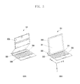
- FIG. 3 is a perspective view illustrating the electronic device 101 according to various embodiments.
- a reference numeral 301 illustrates a perspective view of a first housing 300 when a second housing 340 is not coupled to the first housing 300 according to various embodiments.
- the first housing 300 may include an input module 310 (e.g., the input module 210 ), coupling structure 320 (e.g., the coupling structure 220 ), and cover 330 .
- an input module 310 e.g., the input module 210
- coupling structure 320 e.g., the coupling structure 220
- cover 330 e.g., the cover 330 .
- a surface in which a display 341 is disposed may be referred to as an upper surface and a surface opposite to the upper surface in which the display 341 is disposed may be referred to a lower surface.
- the second housing 340 may include a side member that encloses an upper surface and a lower surface.
- a cover 330 may cover at least a portion of the second housing 340 .
- the cover 330 may include a flexible structure whose at least a portion may bend.
- the cover 330 may include a polyurethane material to provide a flexible structure.
- a reference numeral 302 illustrates a perspective view of the electronic device 101 when the second housing 340 is coupled to the first housing 300 according to various embodiments.
- the second housing 340 may be coupled to at least a portion of a side member and the coupling structure 320 of the first housing 300 .
- the second housing 340 may be coupled to the first housing 300 in a vertical direction of an upper surface of the first housing 300 .
- the first housing 300 may be a plate type, and a surface in which the input module 310 is disposed may be an upper surface, and a surface opposite to the upper surface may be a lower surface.
- the second housing 340 may be coupled to the first housing 300 vertical to the coupling structure 320 .
- the second housing 340 may be coupled to the first housing 300 in a z-axis direction of FIG. 3 .
- FIG. 4 is a diagram illustrating a coupling structure 400 according to various embodiments.
- the coupling structure 400 may be the same as, for example the coupling structure 220 of FIG. 2 and the coupling structure 320 of FIG. 3 .
- the second housing 340 may be coupled to at least a portion of a side member and the coupling structure 400 (e.g., the coupling structure 320 of FIG. 3 ) of the first housing 300 .
- a retainer system 410 may be connected to a moving member such that the first housing 300 forms various support angles.
- FIGS. 5A to 5C are perspective views illustrating an electronic device 101 according to various embodiments.
- a first housing 500 (e.g., the first housing 200 ) of the electronic device 101 may include an input module 510 (e.g., the input module 210 ) and a coupling structure 520 (e.g., the coupling structure 220 ).
- an input module 510 e.g., the input module 210
- a coupling structure 520 e.g., the coupling structure 220
- the first housing 500 (e.g., the first housing 200 ) may be a rectangle in which the width side is longer than the length side.
- the length side of the first housing 500 (e.g., the first housing 200 ) is referred to as an y-axis direction and when the width side of the first housing 500 (e.g., the first housing 200 ) is referred to as an x-axis direction
- the coupling structure 520 (e.g., the coupling structure 220 ) may be disposed in a row in a width direction (e.g., an x-axis direction) of the first housing 500 (e.g., the first housing 200 ).
- the coupling structure 520 (e.g., the coupling structure 220 ) may be disposed at an upper end portion of the keyboard.
- the coupling structure 520 e.g., the coupling structure 220
- the coupling structure 520 may be disposed at an upper surface of the first housing 500 (e.g., the first housing 200 ).
- the first housing 500 (e.g., the first housing 200 ) may be a plate type, and a surface opposite to an upper surface in which the keyboard is disposed may be referred to as a lower surface.
- the first housing 500 (e.g., the first housing 200 ) may include a side member that encloses an upper surface and a lower surface.
- the coupling structure 520 (e.g., the coupling structure 220 ) may be disposed in a width direction along a portion of a side member.
- the coupling structure 520 may include at least one of at least one magnet 521 , at least one pogo structure 522 , at least one electrical connection member 523 , and at least one moving member (not shown).
- the at least one electrical connection member 523 may include an electrical connector that can electrically connect the first housing 500 (e.g., the first housing 200 ) and a second housing 530 of FIG. 5C (e.g., the second housing 230 of FIG. 2 ).
- the electrical connector may include at least one movable conductive pin.
- the coupling structure 520 may include a recess 524 , a moving member (not shown), and retainer systems 522 and 523 .
- the second housing 530 of FIG. 5C e.g., the second housing 230 of FIG. 2
- the first housing 500 e.g., the first housing 200
- at least a portion of a side member of the second housing 530 e.g., the second housing 230
- the recess 524 may be disposed in a width direction along a portion of a side member of the first housing 500 (e.g., the first housing 200 ).
- the moving member may provide a pivotal movement to the second housing 530 (e.g., the second housing 230 ).
- the retainer systems 522 and 523 may maintain a posture such that at least one pogo structure 522 does not float using at least one magnet 521 .
- the second housing 530 may be coupled to at least a portion of the side member and the coupling structure 520 (e.g., the coupling structure 220 ) of the first housing 500 (e.g., the first housing 200 ).
- the second housing 530 e.g., the second housing 230
- the second housing 530 may be coupled to the first housing 500 (e.g., the first housing 200 in a vertical direction of an upper surface of the first housing 500 (e.g., the first housing 200 ).
- the first housing 500 (e.g., the first housing 200 ) may be a plate type, and a surface in which the input module 510 (e.g., the input module 210 ) is disposed may be an upper surface, and a surface opposite to the upper surface may be a lower surface.
- the second housing 530 (e.g., the second housing 230 ) may be coupled to the first housing 500 (e.g., the first housing 200 ) vertical to the coupling structure 520 (e.g., the coupling structure 220 ).
- the coupling structure 520 may be coupled to at least one magnet (not shown) included in the second housing 530 (e.g., the second housing 230 ) using at least one magnet 521 .
- the at least one magnet 521 may be each disposed to have the same polarity in the same direction.
- At least one magnet (not shown) included in the second housing 530 e.g., the second housing 230
- the polarity of at least one magnet 521 and the polarity of at least one magnet (not shown) included in the second housing 530 (e.g., the second housing 230 ) may be opposite.
- the polarity of at least one magnet 521 is an N-pole
- the polarity of at least one magnet (not shown) included in the second housing 530 may be an S-pole.
- FIG. 6 is a perspective view illustrating a state before a first housing 600 and a second housing 630 of the electronic device 101 are coupled according to various embodiments.
- FIG. 7 is a perspective view illustrating a state after the first housing 600 and the second housing 630 of the electronic device 101 are coupled according to various embodiments.
- the first housing 600 may include an input module 610 (e.g., the input module 210 ) and a first coupling structure 620 (e.g., the coupling structure 220 ).
- the second housing 630 may include a display 640 (e.g., the display 231 ) that displays an image.
- the second housing 630 may be a plate type.
- a surface in which the display 640 is disposed may be referred to as an upper surface and a surface opposite to the upper surface in which the display 640 is disposed may be referred to as a lower surface.
- the second housing 630 may include a side member that encloses an upper surface and a lower surface.
- the second housing 630 may include a second coupling structure 631 in at least a portion of a side member. When the first housing 600 and the second housing 630 are coupled, the second coupling structure 631 and the first coupling structure 620 may be coupled.
- the first coupling structure 620 may include a retainer system 621 .
- the retainer system 621 may have a pogo structure.
- the pogo structure may include a socket 622 and a protrusion member 623 .
- the protrusion member 623 may include a socket 622 therein.
- the socket 622 may be coupled to the second coupling structure 631 included in at least a portion of a side member of the second housing 630 .
- the second coupling structure 631 may include a pogo pin member 632 and a recessed member 633 .
- the pogo pin member 632 may be included in the recessed member 633 .
- the recessed member 633 may enable at least a portion (e.g., a plunger) of the pogo pin member 632 to be exposed to the outside.
- the pogo pin member 632 when the first housing 600 and the second housing 630 are coupled, the pogo pin member 632 whose at least a portion (e.g., a plunger) is exposed to the outside may be coupled to the socket 622 .
- a portion of the pogo pin member 632 may be inserted into the socket 622 .
- the protrusion member 623 may be coupled to the recessed member 633 .
- the protrusion member 623 may be inserted into the recessed member 633 .
- FIG. 8 is a perspective view illustrating a magnet disposition of a first housing 801 and a second housing 802 of the electronic device 101 according to various embodiments.
- the electronic device 101 may include a first housing 801 (e.g., the first housing 200 ) and the second housing 802 (e.g., the second housing 230 ).
- the first housing 801 may include a first coupling structure 850 (e.g., the first coupling structure 620 ).
- the second housing 802 may include a second coupling structure 810 (e.g., the second coupling structure 631 ).
- the first coupling structure 850 is extended in a major axis direction of the first housing 801 and may include an extended protrusion member 851 and at least one magnet 852 .
- the at least one magnet 852 may be included within the protrusion member 851 .
- the second coupling structure 810 may include a recessed member (e.g., the recessed member 633 ) extended in at least a partial direction of a side member of the second housing 802 .
- the second coupling structure 810 may include at least one magnet 811 within a recessed member (e.g., the recessed member 633 ).
- At least one magnet 852 of the first coupling structure 850 may be each disposed to have the same polarity in the same direction.
- At least one magnet 811 included in the second coupling structure 810 may be each disposed to have the same polarity in the same direction.
- the polarity of at least one magnet 852 of the first coupling structure 850 and the polarity of at least one magnet 811 included in the second coupling structure 810 may be opposite.
- the polarity of at least one magnet 852 of the first coupling structure 850 is an N-pole
- the polarity of at least one magnet 811 included in the second coupling structure 810 may be an S-pole.
- the first coupling structure 850 may include a moving member connected to the protrusion member 851 , and when the second housing 802 is not coupled to the first housing 801 , in order to prevent a floating or moving phenomenon, a lower portion of the protrusion member 851 may include a magnetic coupling member of a metal material that may be coupled to at least one magnet 852 of the first coupling structure 850 .
- a magnetic force between at least one magnet 852 of the first coupling structure 850 and at least one magnet 811 included in the second coupling structure 810 may be greater than that between at least one magnet 852 of the first coupling structure 850 and a magnetic coupling member of a metal material.
- a magnetic force between at least one magnet 852 of the first coupling structure 850 and a magnetic coupling member of a metal material is 1200G
- a magnetic force between at least one magnet 852 of the first coupling structure 850 and at least one magnet 811 included in the second coupling structure 810 may be 2400G.
- the reason why a magnetic force between at least one magnet 852 of the first coupling structure 850 and at least one magnet 811 included in the second coupling structure 810 is greater than that between at least one magnet 852 of the first coupling structure 850 and a magnetic coupling member of a metal material is to enable the second housing 802 to move in various angles when the first housing 801 and the second housing 802 are coupled.
- At least one pogo structure 860 may be disposed at the center of the first coupling structure 850 , and at least one magnet 852 may be disposed to correspond to at least one magnet 811 included in the second coupling structure 810 based on at least one pogo structure 860 .
- FIG. 9 is a cross-sectional view illustrating a coupling state of a first housing 900 and a second housing 920 of the electronic device 101 according to various embodiments.
- the electronic device 101 may include the first housing 900 (e.g., the first housing 200 ) and the second housing 920 (e.g., the second housing 230 ).
- the first housing 900 may include a first coupling structure 910 (e.g., the first coupling structure 620 ) and a moving member 913 .
- the second housing 920 may include a second coupling structure 921 (e.g., the second coupling structure 631 ).
- the first coupling structure 910 is extended in a major axis direction of the first housing 900 and may include an extended protrusion member 911 and at least one magnet 912 .
- the at least one magnet 912 may be included within the protrusion member 911 .
- the second coupling structure 921 may include a recessed member 923 extended in at least a partial direction of a side member of the second housing 920 .
- the second coupling structure 921 may include at least one magnet 922 therein.
- At least one magnet 912 of the first coupling structure 910 may be each disposed to have the same polarity in the same direction.
- the at least one magnet 922 included in the second coupling structure 921 may be each disposed to have the same polarity in the same direction.
- the first coupling structure 910 and the moving member 913 may be connected to provide a pivotal movement to the second housing 920 .
- At least one moving member 913 may exist and may be made of polyurethane of a flexible material to provide a pivotal movement to the second housing 920 .
- a Flexible Printed Circuit Board (FPCB) 914 may be disposed between at least one moving members 913 .
- the first coupling structure 910 may include the moving member 913 connected to the protrusion member 911 , and when the second housing 920 is not coupled to the first housing 900 , in order to prevent a floating or moving phenomenon, a lower portion of the protrusion member 911 may include a magnetic coupling member of a metal material that may be coupled to at least one magnet 912 .
- FIGS. 10A and 10B are diagrams illustrating a movement of the first coupling structure 910 according to various embodiments.
- the first coupling structure 910 when the first coupling structure 910 is not coupled to the second housing 920 , the first coupling structure 910 may be coupled with a magnetic force to a magnetic coupling member of a metal material disposed at a lower portion of the first coupling structure 910 using at least one magnet 912 included within the protrusion member 911 of the first coupling structure 910 .
- At least one magnet 912 included within the protrusion member 911 of the first coupling structure 910 may be separated from a magnetic coupling member of a metal material disposed at a lower portion of the first coupling structure 910 .
- the moving member 913 connected to the first coupling structure 910 may provide a pivotal movement to the second housing 920 .
- FIG. 11 is a diagram illustrating a movement of the first coupling structure 910 according to various embodiments.
- At least one magnet 912 included within the protrusion member 911 of the first coupling structure 910 may be separated from a magnetic coupling member of a metal material disposed at a lower portion of the first coupling structure 910 .
- the moving member 913 connected to the first coupling structure 910 may provide a pivotal movement to the second housing 920 .
- FIG. 12 is a cross-sectional view illustrating a state when a first housing 1210 (e.g., the first housing 600 ) and a second housing 1220 (e.g., the second housing 630 ) of the electronic device 101 are coupled according to various embodiments.
- a first housing 1210 e.g., the first housing 600
- a second housing 1220 e.g., the second housing 630
- a reference numeral 1230 illustrates a coupling relationship by a magnetic force of at least one magnet 1213 included in the first housing 1210 and at least one magnet 1221 included in the second housing 1220 when the first housing 1210 and the second housing 1220 are coupled.
- the first housing 1210 may include a first coupling structure 1214 (e.g., the first coupling structure 620 ).
- the first coupling structure 1214 may include a protrusion member 1212 (e.g., the protrusion member 623 ) and at least one magnet 1213 .
- the first coupling structure 1214 may be connected to a moving member 1211 (e.g., the moving member 913 ) to provide a pivotal movement to the second housing 1220 .
- the second housing 1220 may include a second coupling structure 1223 (e.g., the second coupling structure 631 ).
- the second coupling structure 1223 may include a recessed member 1222 (e.g., the recessed member 633 ) and at least one magnet 1221 .
- the protrusion member 1212 when the first housing 1210 and the second housing 1220 are coupled, the protrusion member 1212 may be coupled to the recessed member 1222 . When the first housing 1210 and the second housing 1220 are coupled, the protrusion member 1212 may be inserted into the recessed member 1222 .
- a reference numeral 1240 illustrates a coupling relationship of a socket 1216 (e.g., the socket 622 ) included in the first housing 1210 and a pogo pin member 1225 (e.g., the pogo pin member 632 ) included in the second housing 1220 when the first housing 1210 and the second housing 1220 are coupled.
- a socket 1216 e.g., the socket 622
- a pogo pin member 1225 e.g., the pogo pin member 632
- the second coupling structure 1223 may include the pogo pin member 1225 (e.g., the pogo pin member 632 ) and the recessed member 1222 (e.g., the recessed member 633 ).
- the recessed member 1222 may enable at least a portion (e.g., plunger) of the pogo pin member 1225 to be exposed to the outside.
- the pogo pin member 1225 when the first housing 1210 and the second housing 1220 are coupled, the pogo pin member 1225 whose at least a portion (e.g., plunger) is exposed to the outside may be coupled to the socket 1216 .
- a portion of the pogo pin member 1225 may be inserted into the socket 1216 .
- the protrusion member 1212 when the first housing 1210 and the second housing 1220 are coupled, the protrusion member 1212 may be coupled to the recessed member 1222 . When the first housing 1210 and the second housing 1220 are coupled, the protrusion member 1212 may be inserted into the recessed member 1222 .
- FIG. 13 is an exploded perspective view illustrating the first housing 1300 (e.g., the first housing 600 ) of the electronic device 101 according to various embodiments.
- the first housing 1300 may include a keyboard module 1310 and a sliding prevention member 1311 (e.g., rubber, silicon, and fiber) at an upper surface of the outside.
- the sliding prevention member 1311 may be disposed at an upper end portion of the keyboard module 1310 .
- a front case 1320 may be disposed at a low layer of the keyboard module 1310 (e.g., the input module 510 ).
- the front case 1320 may be coupled to a rear case 1330 to form an external appearance of the first housing 1300 .
- the front case 1320 may include the keyboard module 1310 at an upper layer.
- a low layer of the front case 1320 may include at least one of a connection cable 1321 , main board 1322 , click pad 1323 , and first coupling structure 1324 .
- the connection cable 1321 may transfer an electrical signal output from the keyboard module 1310 , main board 1322 , and click pad 1323 to an electrical connector 1414 included in the first coupling structure 1324 .
- the front case 1320 may include a recess extended in a major axis direction that can receive a second housing (e.g., the second housing 630 ) and the first coupling structure 1324 .
- the rear case 1330 is located at a low layer of the front case 1320 and may contain the connection cable 1321 , the main board 1322 , the click pad 1323 , and the first coupling structure 1324 together with the front case 1320 .
- a low layer of the rear case 1330 may include a protection case 1340 .
- the protection case 1340 may be made of a material such as polyurethane or leather.
- FIG. 14 is an exploded perspective view of the first coupling structure 1324 (e.g., the first coupling structure 620 ) of the electronic device 101 according to various embodiments.
- the first coupling structure 1324 may include a protrusion member 1410 (e.g., the protrusion member 623 ), at least one magnet 1411 (e.g., at least one magnet 852 ), a first moving member 1412 (e.g., the moving member 913 ), a second moving member 1413 (e.g., the moving member 913 ), an electrical connector 1414 , at least one pogo structure 1414 (e.g., the pogo structure 860 ), and a magnetic coupling member 1415 (the magnetic coupling member of FIG. 8 ).
- a protrusion member 1410 e.g., the protrusion member 623
- at least one magnet 1411 e.g., at least one magnet 852
- a first moving member 1412 e.g., the moving member 913
- a second moving member 1413 e.g., the moving member 913
- an electrical connector 1414 e.g., at least one pogo structure 1414 (e.g., the po
- the protrusion member 1410 may have a bar shape extended in a major axis direction of the first housing 1300 , and the protrusion member 1410 may perform a cover function of protecting at least one magnet 1411 and at least one pogo structure 1414 included in the first coupling structure 1324 .
- At a low layer of the protrusion member 1410 at least one magnet 1411 may be disposed.
- the first moving member 1412 may be disposed.
- at least one pogo structure 1414 and an electrical connector 1414 may be disposed.
- the at least one pogo structure 1414 and the electrical connector 1414 may be connected.
- the second moving member 1413 At a low layer of the at least one pogo structure 1414 and the electrical connector 1414 , the second moving member 1413 may be disposed.
- a magnetic coupling member 1415 may be disposed.
- the magnetic coupling member 1415 is made of a metal material, and when the second housing (e.g., the second housing 630 ) is not coupled to the first housing 1300 , in order to prevent a floating or moving phenomenon, a lower portion of the protrusion member 1410 may be coupled to the at least one magnet 1411 .
- FIG. 15 is a perspective view illustrating coupling of a keyboard module 1510 (e.g., the keyboard module 1310 ) and a protrusion member 1520 (e.g., the protrusion member 623 ) in the electronic device 101 according to various embodiments.
- a keyboard module 1510 e.g., the keyboard module 1310
- a protrusion member 1520 e.g., the protrusion member 623
- the keyboard module 1510 and the protrusion member 1520 may perform hook coupling 1530 .
- the hook coupling 1530 at least a portion of the keyboard module 1510 may include an extended hook receiving member 1532
- at least a portion of the protrusion member 1520 may include an extended hook protrusion member 1531 .
- the hook coupling 1530 may adjust the protrusion member 1520 .
- the first housing e.g., the first housing 600
- the second housing e.g., the second housing 630
- the hook coupling 1530 is released and thus the second housing (e.g., the second housing 630 ) may move in various angles.
- FIG. 16 is a perspective view illustrating a state when a first housing 1610 (e.g., the first housing 600 ) and a second housing 1620 (e.g., the second housing 630 ) are coupled in the electronic device 101 according to various embodiments.
- a first housing 1610 e.g., the first housing 600
- a second housing 1620 e.g., the second housing 630
- the first housing 1610 and the second housing 1620 may perform hook coupling 1630 .
- a protrusion member 1612 e.g., the protrusion member 623
- an extended hook protrusion member 1632 e.g., the protrusion member 623
- At least a portion of a recessed member 1631 (e.g., the recessed member 633 ) of the second housing 1620 may include an extended hook receiving member.
- the recessed member of the second housing 1620 may be extended in at least a partial direction of a side member of the second housing 1620 .
- FIG. 17 is a perspective view illustrating a second housing 1700 (e.g., the second housing 630 ) including a camera module 1710 at a rear surface and a cover 1721 (e.g., the cover 330 ) that may be extended to one end of a first housing 1720 (e.g., the first housing 600 ) of the electronic device 101 according to various embodiments.
- a second housing 1700 e.g., the second housing 630
- a camera module 1710 at a rear surface
- a cover 1721 e.g., the cover 330
- the cover 1721 may include a hole 1722 that may be coupled to the camera module 1710 .
- At least a portion of the camera module 1710 may be protruded from a rear surface of the second housing 1700 .
- the cover 1722 and the second housing 1700 may be coupled with a binding force.
- FIG. 18 is a perspective view illustrating a second housing 1800 (e.g., the second housing 630 ) including a magnet push button 1811 at a rear surface and a cover 1821 (e.g., the cover 330 ) that may be extended to one end of a first housing (e.g., the first housing 600 ) of the electronic device 101 according to various embodiments.
- a second housing 1800 e.g., the second housing 630
- a cover 1821 e.g., the cover 330
- a rear surface of the second housing 1800 may include a camera module 1810 whose at least a portion is protruded from the rear surface and at least one magnet push button 1811 .
- the at least one magnet push button 1811 may be coupled to correspond to at least one magnet protrusion structure (a magnet protrusion structure 1922 of FIG. 19 ) included in the cover 1821 .
- At least one magnet push button 1811 and at least one magnet protrusion structure may be disposed to correspond.
- At least one magnet push button 1811 and at least one magnet protrusion structure may have opposite magnet polarity.
- At least one magnet push button 1811 may be disposed at a portion of the upper end of a rear surface of the second housing 1800 .
- At least one magnet protrusion structure (a magnet protrusion structure 1922 of FIG. 19 ) may be disposed at a portion of the upper end of the cover 1821 .
- FIG. 19 is a perspective view illustrating a cover 1920 (e.g., the cover 330 and a second housing 1910 (e.g., the second housing 630 ) including the magnet protrusion structure 1922 and that may be extended to one end of a first housing (e.g., the first housing 600 ) of the electronic device 101 according to various embodiments.
- a cover 1920 e.g., the cover 330 and a second housing 1910 (e.g., the second housing 630 ) including the magnet protrusion structure 1922 and that may be extended to one end of a first housing (e.g., the first housing 600 ) of the electronic device 101 according to various embodiments.
- a rear surface of a second housing 1910 may include at least one magnet push button (e.g., the magnet push button 1811 ) and a camera module (e.g., a camera module 1810 ) whose at least a portion is protruded from the rear surface.
- the at least one magnet push button e.g., the magnet push button 1811
- At least one magnet push button (e.g., the magnet push button 1811 ) and at least one magnet protrusion structure 1922 may be disposed to correspond.
- At least one magnet push button (e.g., the magnet push button 1811 ) and at least one magnet protrusion structure 1922 may have opposite magnet polarity.
- At least one magnet push button (e.g., the magnet push button 1811 ) may be disposed at a portion of the upper end of a rear surface of the second housing 1910 .
- At least one magnet protrusion structure 1922 may be disposed at a portion of the upper end of the cover 1920 .
- FIG. 20 is a perspective view illustrating a second housing 2010 (e.g., the second housing 630 ) including a camera module 2011 at a rear surface and a cover 2020 (e.g., the cover 330 ) that may be extended to one end of a first housing 2000 (e.g., the first housing 600 ) of the electronic device 101 according to various embodiments.
- a second housing 2010 e.g., the second housing 630
- a cover 2020 e.g., the cover 330
- the cover 2020 may include a hole 2021 that may be coupled to the camera module 2011 .
- At least a portion of the camera module 2011 may be protruded from a rear surface of the second housing 2010 .
- the cover 2020 and the second housing 2010 may be coupled with a binding force.
- a direct wall may be formed and by disposing a deco at the protruded camera module 2011 , a direct wall may be formed.
- FIG. 21 is a perspective view illustrating a second housing 2110 (e.g., the second housing 2010 ) including a camera module 2111 (e.g., the camera module 2011 ) at a rear surface and the cover 2120 (e.g., the cover 2020 ) that may be extended to one end of a first housing (e.g., first housing 2000 ) of the electronic device 101 according to various embodiments.
- a second housing 2110 e.g., the second housing 2010
- the cover 2120 e.g., the cover 2020
- the cover 2120 may include a hole 2122 that may be coupled to the camera module 2111 .
- At least a portion of the camera module 2111 may be protruded from a rear surface of the second housing 2110 .
- the cover 2120 and the second housing 2110 may be coupled with a binding force.
- a direct wall in order to improve a binding force of the cover 2120 and the second housing 2110 , by disposing at least one first deco 2121 at the hole 2122 of the cover 2120 , a direct wall may be formed, and by disposing a second deco 2112 at the protruded camera module 2111 , a direct wall may be formed.
- FIG. 22 is a perspective view illustrating a second housing 2520 including a magnet push button 2521 at a rear surface and a cover 2500 (e.g., the cover 330 ) that may be extended to one end of a first housing (e.g., the first housing 600 ) of FIGS. 18 and 19 and including a magnet protrusion structure 2510 .
- a cover 2500 e.g., the cover 330
- the magnet protrusion structure 2510 may include a protrusion structure 2511 and at least one magnet 2512 , and may include at least one magnet 2512 within the protrusion structure 2511 .
- the second housing 2520 may include a magnet push button 2521 .
- the magnet push button 2521 may include at least one magnet 2522 , an elastic member 2523 , a protrusion receiving structure 2524 , and a push deco 2525 .
- the protrusion receiving structure 2524 may maintain a shape of the at least one magnet 2522 , the elastic member 2523 , and the push deco 2525 .
- At least one magnet 2522 of the magnet push button 2521 and at least one magnet 2512 of the magnet protrusion structure 2510 having opposite magnet polarity are coupled with a magnetic force, and as the protrusion structure 2511 pushes the push deco 2525 with a magnetic force, an elastic force of the elastic member 2523 is in equilibrium and thus the at least one magnet 2522 and the at least one magnet 2512 are coupled.
- a term “module” used in this document includes a unit configured with hardware, software, or firmware and may be interchangeably used with a term such as a logic, logic block, component, or circuit.
- the “module” may be an integrally configured component or a minimum unit or a portion thereof that performs at least one function.
- the “module” may be implemented mechanically or electronically and may include at least one of, for example an Application-Specific Integrated Circuit (ASIC) chip, Field-Programmable Gate Arrays (FPGAs), and a programmable logic device that perform any operation and that are known or to be developed in the future.
- ASIC Application-Specific Integrated Circuit
- FPGAs Field-Programmable Gate Arrays
- At least a portion of a device (e.g., modules or functions thereof) or a method (e.g., operations) may be implemented with an instruction stored at a computer readable storage medium (e.g., the memory 130 ) in a form of a program module.
- a computer readable storage medium e.g., the memory 130
- the processor may perform a function corresponding to the instruction.
- the computer readable storage medium may be, for example the memory 130 .
- the computer readable recording medium may include a hard disk, floppy disk, magnetic medium (e.g., magnetic tape), optical media (e.g., Compact Disc Read Only Memory (CD-ROM), Digital Versatile Disc (DVD)), magneto-optical media (e.g., floptical disk), and a hardware device (e.g., Read Only Memory (ROM), Random Access Memory (RAM), or flash memory).
- a program instruction may include a high-level language code that may be executed by a computer using an interpreter as well as a machine language code generated by a compiler.
- the above-described hardware device may be configured to operate as at least one software module and vice versa.
- a module or a programming module may include at least one of the foregoing elements, may omit some elements, or may further include additional other elements.
- Operations performed by a module, a programming module, or another constituent element according to various embodiments may be executed with a sequential, parallel, repeated, or heuristic method. Further, some operations may be executed in different orders, may be omitted, or may add other operations.
- Embodiments disclosed in this document are suggested for description and understanding of technology contents and do not limit the scope described in this document. Therefore, it should be analyzed that a range of this document includes entire changes or various other embodiments based on the scope and spirit of this document.
Landscapes
- Engineering & Computer Science (AREA)
- Theoretical Computer Science (AREA)
- Computer Hardware Design (AREA)
- Physics & Mathematics (AREA)
- General Engineering & Computer Science (AREA)
- Human Computer Interaction (AREA)
- General Physics & Mathematics (AREA)
- Mathematical Physics (AREA)
- Casings For Electric Apparatus (AREA)
- Microelectronics & Electronic Packaging (AREA)
Applications Claiming Priority (2)
| Application Number | Priority Date | Filing Date | Title |
|---|---|---|---|
| KR1020150182710A KR102401718B1 (ko) | 2015-12-21 | 2015-12-21 | 결합구조를 포함하는 전자 장치 |
| KR10-2015-0182710 | 2015-12-21 |
Publications (2)
| Publication Number | Publication Date |
|---|---|
| US20170177037A1 US20170177037A1 (en) | 2017-06-22 |
| US10203728B2 true US10203728B2 (en) | 2019-02-12 |
Family
ID=59065174
Family Applications (1)
| Application Number | Title | Priority Date | Filing Date |
|---|---|---|---|
| US15/387,562 Active US10203728B2 (en) | 2015-12-21 | 2016-12-21 | Electronic device including coupling structure |
Country Status (2)
| Country | Link |
|---|---|
| US (1) | US10203728B2 (ko) |
| KR (1) | KR102401718B1 (ko) |
Cited By (3)
| Publication number | Priority date | Publication date | Assignee | Title |
|---|---|---|---|---|
| US10649499B1 (en) * | 2019-05-30 | 2020-05-12 | Hon Hai Precision Industry Co., Ltd. | Electronic device and detachable base |
| US20220004228A1 (en) * | 2019-03-20 | 2022-01-06 | Samsung Electronics Co., Ltd. | Electronic device comprising dual display and keyboard |
| US20220043479A1 (en) * | 2019-04-25 | 2022-02-10 | Hewlett-Packard Development Company, L.P. | Housings with electrical contacts |
Families Citing this family (9)
| Publication number | Priority date | Publication date | Assignee | Title |
|---|---|---|---|---|
| KR102446172B1 (ko) | 2017-10-27 | 2022-09-23 | 삼성전자주식회사 | 입출력 인터페이스를 통해 통신을 수행하는 방법 및 이를 위한 장치 |
| USD873816S1 (en) * | 2017-12-20 | 2020-01-28 | Compal Electronics, Inc. | Notebook computer |
| CN108511241B (zh) * | 2018-05-25 | 2020-06-09 | 高创(苏州)电子有限公司 | 按键结构及具有该按键结构的显示装置 |
| JP1626172S (ko) * | 2018-05-28 | 2019-03-11 | ||
| US10671121B2 (en) * | 2018-09-14 | 2020-06-02 | Apple Inc. | Magnetic layout in electronic devices and accessory devices for electronic devices |
| US10739825B2 (en) | 2018-09-14 | 2020-08-11 | Apple Inc. | Keyboard accessory for a portable electronic device |
| US11126227B2 (en) * | 2018-09-17 | 2021-09-21 | Compal Electronics, Inc. | Electronic device |
| KR20220010921A (ko) * | 2020-07-20 | 2022-01-27 | 삼성전자주식회사 | 전자 펜의 수납을 위한 전자 장치의 커버 |
| KR20220131042A (ko) * | 2021-03-19 | 2022-09-27 | 삼성전자주식회사 | 전자 장치를 위한 커버 장치 |
Citations (11)
| Publication number | Priority date | Publication date | Assignee | Title |
|---|---|---|---|---|
| KR20100005953A (ko) * | 2008-07-08 | 2010-01-18 | 콘티넨탈 오토모티브 시스템 주식회사 | 멀티펑션 스위치를 이용한 차량 시동 방법 및 이에적용되는 장치 |
| KR20110086296A (ko) | 2010-01-22 | 2011-07-28 | 조순미 | 휴대폰 케이스 |
| US20130170131A1 (en) * | 2011-12-28 | 2013-07-04 | Chia-Lian Yen | Docking station for electronic apparatus and connector mechanism therefor |
| US20140111915A1 (en) * | 2012-10-24 | 2014-04-24 | Asustek Computer Inc. | Guiding module and electronic device using the same |
| US20140133080A1 (en) * | 2012-11-15 | 2014-05-15 | Samsung Electronics Co., Ltd. | Detachable electronic device and connection apparatus usable with the same |
| US20140146441A1 (en) * | 2012-11-28 | 2014-05-29 | Nokia Corporation | User-removable device cover |
| KR20150025387A (ko) | 2013-08-29 | 2015-03-10 | 김재욱 | 휴대폰 케이스 |
| US9075566B2 (en) * | 2012-03-02 | 2015-07-07 | Microsoft Technoogy Licensing, LLC | Flexible hinge spine |
| US20150189962A1 (en) | 2014-01-03 | 2015-07-09 | Samsung Electronics Co., Ltd. | Protection cover |
| US20150205330A1 (en) * | 2013-03-29 | 2015-07-23 | Ming Zhang | Electronic device having a detachable tablet |
| US20150268696A1 (en) * | 2014-03-19 | 2015-09-24 | Acer Incorporated | Docking station |
-
2015
- 2015-12-21 KR KR1020150182710A patent/KR102401718B1/ko active IP Right Grant
-
2016
- 2016-12-21 US US15/387,562 patent/US10203728B2/en active Active
Patent Citations (12)
| Publication number | Priority date | Publication date | Assignee | Title |
|---|---|---|---|---|
| KR20100005953A (ko) * | 2008-07-08 | 2010-01-18 | 콘티넨탈 오토모티브 시스템 주식회사 | 멀티펑션 스위치를 이용한 차량 시동 방법 및 이에적용되는 장치 |
| KR20110086296A (ko) | 2010-01-22 | 2011-07-28 | 조순미 | 휴대폰 케이스 |
| US20130170131A1 (en) * | 2011-12-28 | 2013-07-04 | Chia-Lian Yen | Docking station for electronic apparatus and connector mechanism therefor |
| US9075566B2 (en) * | 2012-03-02 | 2015-07-07 | Microsoft Technoogy Licensing, LLC | Flexible hinge spine |
| US20140111915A1 (en) * | 2012-10-24 | 2014-04-24 | Asustek Computer Inc. | Guiding module and electronic device using the same |
| US20140133080A1 (en) * | 2012-11-15 | 2014-05-15 | Samsung Electronics Co., Ltd. | Detachable electronic device and connection apparatus usable with the same |
| US20140146441A1 (en) * | 2012-11-28 | 2014-05-29 | Nokia Corporation | User-removable device cover |
| US20150205330A1 (en) * | 2013-03-29 | 2015-07-23 | Ming Zhang | Electronic device having a detachable tablet |
| KR20150025387A (ko) | 2013-08-29 | 2015-03-10 | 김재욱 | 휴대폰 케이스 |
| US20150189962A1 (en) | 2014-01-03 | 2015-07-09 | Samsung Electronics Co., Ltd. | Protection cover |
| KR20150081213A (ko) | 2014-01-03 | 2015-07-13 | 삼성전자주식회사 | 보호 커버 |
| US20150268696A1 (en) * | 2014-03-19 | 2015-09-24 | Acer Incorporated | Docking station |
Cited By (5)
| Publication number | Priority date | Publication date | Assignee | Title |
|---|---|---|---|---|
| US20220004228A1 (en) * | 2019-03-20 | 2022-01-06 | Samsung Electronics Co., Ltd. | Electronic device comprising dual display and keyboard |
| US11841744B2 (en) * | 2019-03-20 | 2023-12-12 | Samsung Electronics Co., Ltd | Electronic device comprising dual display and keyboard |
| US20220043479A1 (en) * | 2019-04-25 | 2022-02-10 | Hewlett-Packard Development Company, L.P. | Housings with electrical contacts |
| US11703907B2 (en) * | 2019-04-25 | 2023-07-18 | Hewlett-Packard Development Company, L.P. | Housings with electrical contacts |
| US10649499B1 (en) * | 2019-05-30 | 2020-05-12 | Hon Hai Precision Industry Co., Ltd. | Electronic device and detachable base |
Also Published As
| Publication number | Publication date |
|---|---|
| KR20170073924A (ko) | 2017-06-29 |
| US20170177037A1 (en) | 2017-06-22 |
| KR102401718B1 (ko) | 2022-05-26 |
Similar Documents
| Publication | Publication Date | Title |
|---|---|---|
| US10203728B2 (en) | Electronic device including coupling structure | |
| KR102449165B1 (ko) | 하우징을 포함하는 전자 장치 | |
| EP3209013B1 (en) | Electronic device and method for manufacturing the same | |
| US10459493B2 (en) | Electronic device including plurality of housings | |
| KR102500141B1 (ko) | 개선된 체결 구조를 갖는 스트랩 및 그것을 포함하는 웨어러블 전자 장치 | |
| US11013150B2 (en) | Electronic device comprising heat dissipation structure | |
| US20160081204A1 (en) | Electronic device including flexible display element | |
| KR102376981B1 (ko) | 방열 구조를 갖는 전자 장치 | |
| CN105433519B (zh) | 可穿戴设备的搭扣装置 | |
| US10638632B2 (en) | Electronic device including cable fixing apparatus | |
| KR102622733B1 (ko) | 플렉시블 커넥터를 포함하는 전자 장치 | |
| KR102550590B1 (ko) | 커넥터 및 이를 포함하는 전자 장치 | |
| US10777920B2 (en) | Connecting device and electronic device including the same | |
| US10547140B2 (en) | Connecting component with waterproof device and electronic device including the same | |
| US11337326B2 (en) | Electronic device with a switch to prevent over-discharging of device battery | |
| US11159034B2 (en) | Wireless charging stand, and method for operating electronic device linked thereto | |
| US11362452B2 (en) | Multi-connection device | |
| KR102499108B1 (ko) | 전자 장치, 전자 장치의 전력 공급 장치 및 전력 공급 방법 | |
| EP3578078B1 (en) | Accessory device comprising printed circuit board having flexible structure | |
| KR20160024444A (ko) | 전자장치 케이스 및 이를 구비하는 전자장치 |
Legal Events
| Date | Code | Title | Description |
|---|---|---|---|
| AS | Assignment |
Owner name: SAMSUNG ELECTRONICS CO., LTD, KOREA, REPUBLIC OF Free format text: ASSIGNMENT OF ASSIGNORS INTEREST;ASSIGNORS:KOO, YOUNGGWON;PARK, JINYOUNG;LEE, SEUNGWOON;AND OTHERS;REEL/FRAME:041172/0380 Effective date: 20161206 |
|
| STCF | Information on status: patent grant |
Free format text: PATENTED CASE |
|
| MAFP | Maintenance fee payment |
Free format text: PAYMENT OF MAINTENANCE FEE, 4TH YEAR, LARGE ENTITY (ORIGINAL EVENT CODE: M1551); ENTITY STATUS OF PATENT OWNER: LARGE ENTITY Year of fee payment: 4 |