US10074794B2 - Multilayer component comprising an external contact and method for producing a multilayer component comprising an external contact - Google Patents
Multilayer component comprising an external contact and method for producing a multilayer component comprising an external contact Download PDFInfo
- Publication number
- US10074794B2 US10074794B2 US14/907,800 US201414907800A US10074794B2 US 10074794 B2 US10074794 B2 US 10074794B2 US 201414907800 A US201414907800 A US 201414907800A US 10074794 B2 US10074794 B2 US 10074794B2
- Authority
- US
- United States
- Prior art keywords
- contact layer
- multilayer component
- main body
- component according
- connection element
- Prior art date
- Legal status (The legal status is an assumption and is not a legal conclusion. Google has not performed a legal analysis and makes no representation as to the accuracy of the status listed.)
- Expired - Fee Related, expires
Links
Images

Classifications
-
- H01L41/0472—
-
- B—PERFORMING OPERATIONS; TRANSPORTING
- B23—MACHINE TOOLS; METAL-WORKING NOT OTHERWISE PROVIDED FOR
- B23K—SOLDERING OR UNSOLDERING; WELDING; CLADDING OR PLATING BY SOLDERING OR WELDING; CUTTING BY APPLYING HEAT LOCALLY, e.g. FLAME CUTTING; WORKING BY LASER BEAM
- B23K1/00—Soldering, e.g. brazing, or unsoldering
- B23K1/0008—Soldering, e.g. brazing, or unsoldering specially adapted for particular articles or work
- B23K1/0016—Soldering of electronic components
-
- H—ELECTRICITY
- H01—ELECTRIC ELEMENTS
- H01C—RESISTORS
- H01C1/00—Details
- H01C1/14—Terminals or tapping points specially adapted for resistors; Arrangements of terminals or tapping points on resistors
-
- H—ELECTRICITY
- H01—ELECTRIC ELEMENTS
- H01C—RESISTORS
- H01C17/00—Apparatus or processes specially adapted for manufacturing resistors
- H01C17/28—Apparatus or processes specially adapted for manufacturing resistors adapted for applying terminals
-
- H—ELECTRICITY
- H01—ELECTRIC ELEMENTS
- H01C—RESISTORS
- H01C7/00—Non-adjustable resistors formed as one or more layers or coatings; Non-adjustable resistors made from powdered conducting material or powdered semi-conducting material with or without insulating material
- H01C7/10—Non-adjustable resistors formed as one or more layers or coatings; Non-adjustable resistors made from powdered conducting material or powdered semi-conducting material with or without insulating material voltage responsive, i.e. varistors
-
- H—ELECTRICITY
- H01—ELECTRIC ELEMENTS
- H01G—CAPACITORS; CAPACITORS, RECTIFIERS, DETECTORS, SWITCHING DEVICES, LIGHT-SENSITIVE OR TEMPERATURE-SENSITIVE DEVICES OF THE ELECTROLYTIC TYPE
- H01G13/00—Apparatus specially adapted for manufacturing capacitors; Processes specially adapted for manufacturing capacitors not provided for in groups H01G4/00 - H01G11/00
- H01G13/006—Apparatus or processes for applying terminals
-
- H—ELECTRICITY
- H01—ELECTRIC ELEMENTS
- H01G—CAPACITORS; CAPACITORS, RECTIFIERS, DETECTORS, SWITCHING DEVICES, LIGHT-SENSITIVE OR TEMPERATURE-SENSITIVE DEVICES OF THE ELECTROLYTIC TYPE
- H01G4/00—Fixed capacitors; Processes of their manufacture
- H01G4/002—Details
- H01G4/005—Electrodes
- H01G4/008—Selection of materials
-
- H—ELECTRICITY
- H01—ELECTRIC ELEMENTS
- H01G—CAPACITORS; CAPACITORS, RECTIFIERS, DETECTORS, SWITCHING DEVICES, LIGHT-SENSITIVE OR TEMPERATURE-SENSITIVE DEVICES OF THE ELECTROLYTIC TYPE
- H01G4/00—Fixed capacitors; Processes of their manufacture
- H01G4/002—Details
- H01G4/228—Terminals
- H01G4/232—Terminals electrically connecting two or more layers of a stacked or rolled capacitor
-
- H—ELECTRICITY
- H01—ELECTRIC ELEMENTS
- H01G—CAPACITORS; CAPACITORS, RECTIFIERS, DETECTORS, SWITCHING DEVICES, LIGHT-SENSITIVE OR TEMPERATURE-SENSITIVE DEVICES OF THE ELECTROLYTIC TYPE
- H01G4/00—Fixed capacitors; Processes of their manufacture
- H01G4/002—Details
- H01G4/228—Terminals
- H01G4/232—Terminals electrically connecting two or more layers of a stacked or rolled capacitor
- H01G4/2325—Terminals electrically connecting two or more layers of a stacked or rolled capacitor characterised by the material of the terminals
-
- H—ELECTRICITY
- H01—ELECTRIC ELEMENTS
- H01G—CAPACITORS; CAPACITORS, RECTIFIERS, DETECTORS, SWITCHING DEVICES, LIGHT-SENSITIVE OR TEMPERATURE-SENSITIVE DEVICES OF THE ELECTROLYTIC TYPE
- H01G4/00—Fixed capacitors; Processes of their manufacture
- H01G4/30—Stacked capacitors
-
- H01L41/293—
-
- H—ELECTRICITY
- H10—SEMICONDUCTOR DEVICES; ELECTRIC SOLID-STATE DEVICES NOT OTHERWISE PROVIDED FOR
- H10N—ELECTRIC SOLID-STATE DEVICES NOT OTHERWISE PROVIDED FOR
- H10N30/00—Piezoelectric or electrostrictive devices
- H10N30/01—Manufacture or treatment
- H10N30/06—Forming electrodes or interconnections, e.g. leads or terminals
- H10N30/063—Forming interconnections, e.g. connection electrodes of multilayered piezoelectric or electrostrictive parts
-
- H—ELECTRICITY
- H10—SEMICONDUCTOR DEVICES; ELECTRIC SOLID-STATE DEVICES NOT OTHERWISE PROVIDED FOR
- H10N—ELECTRIC SOLID-STATE DEVICES NOT OTHERWISE PROVIDED FOR
- H10N30/00—Piezoelectric or electrostrictive devices
- H10N30/80—Constructional details
- H10N30/87—Electrodes or interconnections, e.g. leads or terminals
- H10N30/872—Interconnections, e.g. connection electrodes of multilayer piezoelectric or electrostrictive devices
-
- H—ELECTRICITY
- H01—ELECTRIC ELEMENTS
- H01G—CAPACITORS; CAPACITORS, RECTIFIERS, DETECTORS, SWITCHING DEVICES, LIGHT-SENSITIVE OR TEMPERATURE-SENSITIVE DEVICES OF THE ELECTROLYTIC TYPE
- H01G4/00—Fixed capacitors; Processes of their manufacture
- H01G4/002—Details
- H01G4/228—Terminals
Definitions
- Embodiments of the invention relate to a multilayer component comprising an external contact and method for producing a multilayer component comprising an external contact.
- connection element For contacting a multilayer component, by way of example, a connection element is soldered, adhesively bonded or welded to a main body. In the case of such fixing however, the contacting can influence the movements of the actuator. Moreover, the contacting can be damaged by the frequent deflection of the actuator.
- a multilayer component comprising an external contact is specified.
- the multilayer component is a piezoactuator that can be used for actuating an injection valve in a motor vehicle.
- the multilayer component can be for example a multilayer capacitor or a multilayer varistor.
- Embodiments specify an improved multilayer component. Particular embodiments specify a particularly reliable multilayer component.
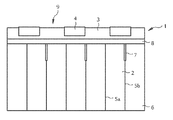
- FIG. 1 shows a sectional illustration of a multilayer component
- FIG. 2 shows a side view of the multilayer component from FIG. 1 .
- a multilayer component comprising a main body and an external contact.
- the external contact has a connection element and a contact layer.
- the contact layer electrically conductively connects the main body to the connection element.
- a connection between the main body and the connection element is produced by sintering of the contact layer.
- the temperature during sintering is preferably less than 400° C.
- the contact layer is sintered at 250° C.
- the sintered contact layer has a polycrystalline microstructure.
- grains and grain boundaries are formed in the sintered contact layer.
- pores and/or sintering necks are formed in the sintered contact layer.
- the pores and/or sintering necks are formed, for example, between metal particles, or between grains.
- a sintered contact layer has the advantage that it has a high electrical conductivity. Moreover, a sintered contact layer has a high thermal conductivity. In particular, a sintered contact layer has a higher electrical conductivity and a higher thermal conductivity than solders, for example, in particular soft solders. Furthermore, the sintered contact layer exhibits low material fatigue at high temperatures. In particular, only a slight plastic reshaping of the contact layer and a slight crack growth in the contact layer take place. This is owed to a high melting point of the contact layer in comparison with solders. Even in the event of mechanical or thermomechanical cyclic load, only low material fatigue of the contact layer occurs.
- multilayer components having such a contact layer can be soldered on circuit boards in a reflow process.
- the sintering of the contact layer can take place without the use of fluxes. Therefore, there is also no need for a washing process for removing flux residues, as required, for example, in the case of soldering.
- the process temperature during the sintering of the contact layer is significantly lower than during hard soldering or during firing of metal pastes. As a result, the thermal stress in the process is relatively low and the process is simpler and more cost-effective.
- the contact layer is porous.
- the contact layer has a porosity of between 1 percent by volume and 50 percent by volume.
- the modulus of elasticity of the contact layer is lower than in the case of impermeable metal layers. As a result, it is possible to reduce clamping effects and mechanical stresses in the ceramic body.
- the contact layer comprises a metal.
- the contact layer preferably consists of silver or copper.
- the contact layer consists of pure silver or copper to the extent of at least 95 percent by weight, preferably to the extent of 99 percent by weight.
- the contact layer can consist of pure silver or copper to the extent of at least 99% by weight.
- the melting point of the metal of the contact layer is above the sintering temperature of the contact layer.
- the melting point of the contact layer is above 400° C.
- the contact layer has a high thermal stability at operating temperatures above 200° C.
- the contact layer has a thickness of between 2 ⁇ m and 200 ⁇ m.
- the contact layer has a thickness of between 10 ⁇ m and 100 ⁇ m.
- the main body of the multilayer component can comprise a stack of dielectric layers and internal electrode layers.
- the external contact can serve for electrically contacting the internal electrode layers.
- the main body is embodied in a parallelepipedal fashion, for example.
- the dielectric layers and the internal electrode layers are stacked along a stacking direction.
- the stacking direction preferably corresponds to the longitudinal direction of the main body.
- the dielectric layers and the internal electrode layers are stacked alternately one above another.
- the internal electrode layers contain copper or consist of copper.
- the internal electrode layers contain silver-palladium or consist of silver-palladium.
- the dielectric layers can comprise a piezoelectric material.
- the dielectric layers can comprise a ceramic material, in particular a piezoceramic material.
- Green sheets can be used for producing the main body, wherein a metal paste, for example, is applied to the green sheets for the purpose of forming internal electrode layers.
- the metal paste is applied in a screen printing method.
- the metal paste can contain copper.
- the metal paste can contain silver or silver-palladium.
- the sheets are preferably stacked, pressed and jointly sintered, thus giving rise to a monolithic sintering body.
- the main body of the component is formed by a monolithic sintering body, for example, by a sintering body produced in the manner described above.
- the multilayer component is embodied as a piezoelectric component, for example, as a piezoactuator.
- a piezoactuator piezoelectric layers arranged between the internal electrode layers expand when a voltage is applied to the internal electrode layers, such that a stroke of the piezoactuator is generated.
- the multilayer component can also be embodied as some other component, for example, as a multilayer capacitor.
- the multilayer capacitor is preferably suitable for power electronic applications with DC voltages of greater than 250 volts and use temperatures above 120° C.
- the external contact preferably serves for applying a voltage between internal electrode layers that are adjacent in the stacking direction.
- the external contact serves for feeding current to the internal electrode layers.
- two external electrodes are arranged on opposite outer sides of the main body.
- An external electrode in each case comprises a contact layer and a connection element.
- the internal electrode layers are electrically connected to one of the external electrodes and electrically insulated from the other external electrode alternately in the stacking direction.
- the external contact can be designed with regard to the loadings at the main body.
- the electrode paste is applied such that the electrode layers, alternately as viewed in the stacking direction, extend as far as one outer side of the stack and are spaced apart from the opposite outer side of the stack.
- the electrode layers can be electrically connected alternately to one of the external contacts.
- an air gap can be present between one end of the internal electrode layer and an outer side of the main body.
- alternately every second internal electrode layer can be set back by means of etching, such that a trench is arranged between the etched internal electrode layers and an outer side of the main body.
- the air gaps or the trenches can be filled with insulating material.
- the insulating material can be an elastomeric material, for example.
- the trenches can be almost completely filled with insulating material. This results from the fact that the use of a flux can be dispensed with. As a result, no flux residues which make it more difficult for the trenches to be filled or prevent the trenches from being filled can remain in the trenches. In this way, the breakdown voltage of the multilayer component can be increased by approximately 10% in comparison with a multilayer component comprising a soldered external contact.
- the multilayer component can be a fully active multilayer component.
- the internal electrode layers extend over the entire cross section of the main body.
- the internal electrode layers are alternately covered with electrically insulating material on an outer side.
- the internal electrode layers are electrically connected to one of the external electrodes and electrically insulated from the other external electrode alternately in the stacking direction.
- the external contact is embodied in a strip-shaped fashion, for example.
- the external contact runs along the stacking direction of the main body.
- the external contact only partly covers an outer side of the main body.
- the external contact can completely cover an outer side of the main body.
- connection elements can have the shape of a planar body or the shape of a three-dimensionally structured body.
- a planar body can have, for example, the shape of a metal sheet, a meander, a comb or a conductor.
- a three-dimensionally structured body can have, for example, the shape of a wire braiding, a knitted wire mesh or a corrugated metal sheet.
- connection elements preferably extend over the entire length of the multilayer component.
- a base metallization is additionally applied between the main body and the contact layer.
- the base metallization can be formed by firing a metal paste.
- the base metallization can be linked to the contact layer by sintering.
- the base metallization can be admixed with a glass paste.
- the base metallization can be applied to the main body by the sputtering of metal layers and can be linked to the contact layer by sintering. Accordingly, the base metallization can consist only of a layer applied by sputtering.
- the base metallization can be formed a by firing of a metal paste and by an additional sputtering layer between the fired metal paste and the contact layer.
- a method for producing a multilayer component comprises, in a first step, providing a main body and a connection element. Afterwards, a metal paste is applied to at least one outer side of the main body. The connection element is positioned on the metal paste. In particular, the connection element can be at least partly pressed into the metal paste. Afterwards, the metal paste is sintered. The sintering is carried out at a temperature below 400° C. As a result, the connection element is electrically conductively connected to the main body.
- the metal paste can contain metal particles, salts and organic material as solvent and coating material of the solids.
- the metal particles are silver or copper particles, for example.
- Silver carbonate, for example, is suitable as salt.
- the metal paste is applied using a stencil, for example.
- the applied layer of the metal paste is preferably 1 mm wide and 100 ⁇ m thick.
- the contact layer is dried and sintered.
- the metal paste is subjected to binder removal for 75 minutes at 160° C. and is then sintered for 105 minutes at 250° C.
- the sintering can be carried out under pressure or without pressure.
- the contact layer is present as a solid, porous, pure metal layer.
- the main body and the external contact are fixedly linked to the contact layer.
- the metal paste is converted to the porous contact layer.
- FIG. 1 shows a multilayer component 1 in a sectional illustration.
- the multilayer component 1 comprises a main body 2 .
- the main body 2 comprises alternately arranged first and second internal electrode layers 5 a , 5 b and piezoelectric layers 6 .
- the external contact 9 is applied on an outer side of the main body 2 .
- the external contact 9 comprises a contact layer 3 and a connection element 4 .
- the contact layer 3 is porous.
- the external contact 9 comprises a base metallization 8 .
- the base metallization 8 can comprise, for example, a fired metal layer and/or a sputtering layer.
- the fired metal layer can comprise a glass additive.
- Every first internal electrode layer 5 a extends as far as the outer side of the main body 2 and is contacted there by the external contact 9 .
- Every second internal electrode layer 5 b is spaced apart from the outer side of the main body 2 .
- an insulation zone 7 is arranged between every second internal electrode layer 5 b and the outer side of the main body.
- the insulation zone 7 can be embodied as an air gap.
- the insulation zone 7 can be filled with an insulating material.
- connection element 4 is at least partly embedded into the contact layer 3 .
- a reliable connection between the connection element 4 and the contact layer 3 is produced as a result.
- FIG. 2 shows the multilayer component 1 in a side view.
- every second internal electrode layer 5 b which is spaced apart from the outer side of the main body 2 by an insulation zone 7 is illustrated by dashed lines.
- the second internal electrode layers 5 b extend as far as the outer side of the main body 2 , while the first internal electrode layers 5 a are spaced apart therefrom by an insulation zone 7 .
- the base metallization 8 and the contact layer 3 are embodied in the form of a strip, wherein the base metallization 8 is somewhat wider than the contact layer 3 .
- connection element 4 shown in FIG. 2 is embodied in a meandering fashion.
- connection element 4 can also have other shapes, for example, that of a conductor, a metal sheet or corrugated metal sheet, a wire screen or a comb.
Landscapes
- Engineering & Computer Science (AREA)
- Power Engineering (AREA)
- Microelectronics & Electronic Packaging (AREA)
- Manufacturing & Machinery (AREA)
- Mechanical Engineering (AREA)
- Materials Engineering (AREA)
- Chemical & Material Sciences (AREA)
- Physics & Mathematics (AREA)
- Electromagnetism (AREA)
- Ceramic Capacitors (AREA)
- Micromachines (AREA)
- Contacts (AREA)
- Production Of Multi-Layered Print Wiring Board (AREA)
- Laminated Bodies (AREA)
- General Electrical Machinery Utilizing Piezoelectricity, Electrostriction Or Magnetostriction (AREA)
Applications Claiming Priority (4)
| Application Number | Priority Date | Filing Date | Title |
|---|---|---|---|
| DE102013108753 | 2013-08-13 | ||
| DE102013108753.1A DE102013108753A1 (de) | 2013-08-13 | 2013-08-13 | Vielschichtbauelement mit einer Außenkontaktierung und Verfahren zur Herstellung eines Vielschichtbauelements mit einer Außenkontaktierung |
| DE102013108753.1 | 2013-08-13 | ||
| PCT/EP2014/065746 WO2015022154A1 (de) | 2013-08-13 | 2014-07-22 | VIELSCHICHTBAUELEMENT MIT EINER AUßENKONTAKTIERUNG UND VERFAHREN ZUR HERSTELLUNG EINES VIELSCHICHTBAUELEMENTS MIT EINER AUßENKONTAKTIERUNG |
Publications (2)
| Publication Number | Publication Date |
|---|---|
| US20160190424A1 US20160190424A1 (en) | 2016-06-30 |
| US10074794B2 true US10074794B2 (en) | 2018-09-11 |
Family
ID=51211793
Family Applications (1)
| Application Number | Title | Priority Date | Filing Date |
|---|---|---|---|
| US14/907,800 Expired - Fee Related US10074794B2 (en) | 2013-08-13 | 2014-07-22 | Multilayer component comprising an external contact and method for producing a multilayer component comprising an external contact |
Country Status (6)
| Country | Link |
|---|---|
| US (1) | US10074794B2 (de) |
| EP (1) | EP3033756B1 (de) |
| JP (1) | JP6240775B2 (de) |
| CN (1) | CN105431917B (de) |
| DE (1) | DE102013108753A1 (de) |
| WO (1) | WO2015022154A1 (de) |
Families Citing this family (4)
| Publication number | Priority date | Publication date | Assignee | Title |
|---|---|---|---|---|
| DE102015102866B4 (de) | 2015-02-27 | 2023-02-02 | Tdk Electronics Ag | Keramisches Bauelement, Bauelementanordnung und Verfahren zur Herstellung eines keramischen Bauelements |
| DE102015017344B3 (de) | 2015-02-27 | 2024-10-24 | Tdk Electronics Ag | Keramisches Bauelement, Bauelementanordnung und Verfahren zur Herstellung eines keramischen Bauelemements |
| DE102020118859B4 (de) | 2020-07-16 | 2024-10-02 | Tdk Electronics Ag | Keramikmaterial für Kondensator sowie Kondensator |
| DE102020118857B4 (de) | 2020-07-16 | 2023-10-26 | Tdk Electronics Ag | Vielschichtkondensator |
Citations (27)
| Publication number | Priority date | Publication date | Assignee | Title |
|---|---|---|---|---|
| US4559279A (en) * | 1983-06-30 | 1985-12-17 | Matsushita Electric Industrial Co., Ltd. | Electrode on heat-resisting and isolating substrate |
| US20020043901A1 (en) * | 2000-12-28 | 2002-04-18 | Noriaki Kihara | Multilayer-type piezoelectric actuator |
| US6411018B1 (en) * | 1999-06-19 | 2002-06-25 | Robert Bosch Gmbh | Piezoelectric actuator with improved electrode connections |
| WO2005029602A1 (ja) | 2003-09-24 | 2005-03-31 | Kyocera Corporation | 積層型圧電素子 |
| JP2005101207A (ja) | 2003-09-24 | 2005-04-14 | Kyocera Corp | 積層型圧電素子及びその製法並びに噴射装置 |
| DE102004002484A1 (de) | 2004-01-17 | 2005-08-11 | Robert Bosch Gmbh | Piezoaktor mit einer elektrisch leitfähigen Kontaktfahne |
| WO2005086247A1 (ja) | 2004-03-09 | 2005-09-15 | Kyocera Corporation | 積層型圧電素子とその製造方法 |
| US20050280336A1 (en) * | 2004-06-18 | 2005-12-22 | Tdk Corporation | Multilayer piezoelectric element |
| JP2006013437A (ja) | 2004-05-27 | 2006-01-12 | Kyocera Corp | 積層型圧電素子およびその製造方法ならびにこれを用いた噴射装置 |
| JP2006157259A (ja) | 2004-11-26 | 2006-06-15 | Kyocera Corp | 薄膜バルク音響波共振子およびフィルタならびに通信装置 |
| DE102005017108A1 (de) | 2005-01-26 | 2006-07-27 | Epcos Ag | Piezoelektrisches Bauelement |
| US20060232172A1 (en) * | 2005-04-18 | 2006-10-19 | Denso Corporation | Laminated-type piezoelectric element |
| DE102005027364A1 (de) | 2005-06-14 | 2006-12-21 | Robert Bosch Gmbh | Piezoaktor |
| EP1780813A1 (de) | 2004-06-24 | 2007-05-02 | Kyocera Corporation | Mehrschichtige elektronische komponente und injektionssystem damit |
| CN1973384A (zh) | 2004-06-24 | 2007-05-30 | 京瓷株式会社 | 叠层型电子部件及使用其的喷射装置 |
| WO2007118883A1 (de) | 2006-04-19 | 2007-10-25 | Robert Bosch Gmbh | Piezoaktor und verfahren zu dessen herstellung |
| DE102007049145A1 (de) | 2007-10-12 | 2009-04-16 | Robert Bosch Gmbh | Piezoaktor und Verfahren zu dessen Herstellung |
| CN101431038A (zh) | 2007-09-28 | 2009-05-13 | W.C.贺利氏有限公司 | 用于多个金属面触点接通的方法和膏体 |
| JP2010065277A (ja) | 2008-09-10 | 2010-03-25 | Nippon Handa Kk | 金属製部材接合体の製造方法および金属製部材接合体 |
| DE102008056746A1 (de) | 2008-11-11 | 2010-05-12 | Epcos Ag | Piezoaktor in Vielschichtbauweise und Verfahren zur Befestigung einer Außenelektrode bei einem Piezoaktor |
| JP2010123647A (ja) | 2008-11-18 | 2010-06-03 | Panasonic Corp | セラミックス電子部品、及びこれを用いた電子機器 |
| DE102008055144A1 (de) | 2008-12-23 | 2010-07-01 | Robert Bosch Gmbh | Piezoaktor, Kraftstoff-Injetor mit Piezoaktor sowie Verfahren zum Herstellen eines Piezoaktors |
| DE102010044326A1 (de) | 2010-09-03 | 2012-03-08 | Heraeus Materials Technology Gmbh & Co. Kg | Verwendung von aliphatischen Kohlenwasserstoffen und Paraffinen als Lösemittel in Silbersinterpasten |
| US20120132729A1 (en) * | 2009-05-26 | 2012-05-31 | Kyocera Corporation | Multi-Layer Piezoelectric Element, and Injection Device and Fuel Injection System Incorporating the Multi-Layer Piezoelectric Element |
| US20130140960A1 (en) * | 2010-06-07 | 2013-06-06 | Epcos Ag | Piezoelectric Multilayer Component and Method for Forming an External Electrode in a Piezoelectric Multilayer Component |
| US20150300894A1 (en) * | 2013-09-06 | 2015-10-22 | Schlumberger Technology Corporation | Piezoelectric actuator and process for manufacturing same |
| US20170372820A1 (en) * | 2015-11-27 | 2017-12-28 | Epcos Ag | Multilayer Component and Process for Producing Multilayer Component |
-
2013
- 2013-08-13 DE DE102013108753.1A patent/DE102013108753A1/de not_active Ceased
-
2014
- 2014-07-22 CN CN201480045341.9A patent/CN105431917B/zh active Active
- 2014-07-22 JP JP2016533865A patent/JP6240775B2/ja active Active
- 2014-07-22 US US14/907,800 patent/US10074794B2/en not_active Expired - Fee Related
- 2014-07-22 WO PCT/EP2014/065746 patent/WO2015022154A1/de not_active Ceased
- 2014-07-22 EP EP14741642.4A patent/EP3033756B1/de active Active
Patent Citations (39)
| Publication number | Priority date | Publication date | Assignee | Title |
|---|---|---|---|---|
| US4559279A (en) * | 1983-06-30 | 1985-12-17 | Matsushita Electric Industrial Co., Ltd. | Electrode on heat-resisting and isolating substrate |
| US6411018B1 (en) * | 1999-06-19 | 2002-06-25 | Robert Bosch Gmbh | Piezoelectric actuator with improved electrode connections |
| US20020043901A1 (en) * | 2000-12-28 | 2002-04-18 | Noriaki Kihara | Multilayer-type piezoelectric actuator |
| EP1675190A1 (de) | 2003-09-24 | 2006-06-28 | Kyocera Corporation | Mehrschichtiges piezoelektrisches bauelement |
| WO2005029602A1 (ja) | 2003-09-24 | 2005-03-31 | Kyocera Corporation | 積層型圧電素子 |
| JP2005101207A (ja) | 2003-09-24 | 2005-04-14 | Kyocera Corp | 積層型圧電素子及びその製法並びに噴射装置 |
| US8004155B2 (en) | 2003-09-24 | 2011-08-23 | Kyocera Corporation | Multi-layer piezoelectric element |
| US20070176521A1 (en) | 2003-09-24 | 2007-08-02 | Shigenobu Nakamura | Multi-layer piezoelectric element |
| DE102004002484A1 (de) | 2004-01-17 | 2005-08-11 | Robert Bosch Gmbh | Piezoaktor mit einer elektrisch leitfähigen Kontaktfahne |
| EP1732146A1 (de) | 2004-03-09 | 2006-12-13 | Kyocera Corporation | Mehrschichtiges piezoelektrisches element und herstellungsverfahren dafür |
| WO2005086247A1 (ja) | 2004-03-09 | 2005-09-15 | Kyocera Corporation | 積層型圧電素子とその製造方法 |
| US20070278907A1 (en) | 2004-03-09 | 2007-12-06 | Kyocera Corporation | Multi-Layer Piezoelectric Element and Method for Manufacturing the Same |
| JP2006013437A (ja) | 2004-05-27 | 2006-01-12 | Kyocera Corp | 積層型圧電素子およびその製造方法ならびにこれを用いた噴射装置 |
| US20050280336A1 (en) * | 2004-06-18 | 2005-12-22 | Tdk Corporation | Multilayer piezoelectric element |
| EP1780813A1 (de) | 2004-06-24 | 2007-05-02 | Kyocera Corporation | Mehrschichtige elektronische komponente und injektionssystem damit |
| CN1973384A (zh) | 2004-06-24 | 2007-05-30 | 京瓷株式会社 | 叠层型电子部件及使用其的喷射装置 |
| JP2006157259A (ja) | 2004-11-26 | 2006-06-15 | Kyocera Corp | 薄膜バルク音響波共振子およびフィルタならびに通信装置 |
| DE102005017108A1 (de) | 2005-01-26 | 2006-07-27 | Epcos Ag | Piezoelektrisches Bauelement |
| US7868524B2 (en) | 2005-01-26 | 2011-01-11 | Epcos Ag | Piezoelectric component |
| US20060232172A1 (en) * | 2005-04-18 | 2006-10-19 | Denso Corporation | Laminated-type piezoelectric element |
| DE102005027364A1 (de) | 2005-06-14 | 2006-12-21 | Robert Bosch Gmbh | Piezoaktor |
| WO2007118883A1 (de) | 2006-04-19 | 2007-10-25 | Robert Bosch Gmbh | Piezoaktor und verfahren zu dessen herstellung |
| US20100156251A1 (en) | 2006-04-19 | 2010-06-24 | Eugen Hohmann | Piezoelectric actuator and method for producing it |
| JP2009534825A (ja) | 2006-04-19 | 2009-09-24 | ローベルト ボツシユ ゲゼルシヤフト ミツト ベシユレンクテル ハフツング | 圧電アクチュエータおよびその作製方法 |
| DE102006018034A1 (de) | 2006-04-19 | 2007-10-31 | Robert Bosch Gmbh | Piezoaktor und Verfahren zu dessen Herstellung |
| CN101431038A (zh) | 2007-09-28 | 2009-05-13 | W.C.贺利氏有限公司 | 用于多个金属面触点接通的方法和膏体 |
| DE102007049145A1 (de) | 2007-10-12 | 2009-04-16 | Robert Bosch Gmbh | Piezoaktor und Verfahren zu dessen Herstellung |
| JP2010065277A (ja) | 2008-09-10 | 2010-03-25 | Nippon Handa Kk | 金属製部材接合体の製造方法および金属製部材接合体 |
| WO2010055071A1 (de) | 2008-11-11 | 2010-05-20 | Epcos Ag | Piezoaktor in vielschichtbauweise und verfahren zur befestigung einer aussenelektrode bei einem piezoaktor |
| DE102008056746A1 (de) | 2008-11-11 | 2010-05-12 | Epcos Ag | Piezoaktor in Vielschichtbauweise und Verfahren zur Befestigung einer Außenelektrode bei einem Piezoaktor |
| US9059392B2 (en) | 2008-11-11 | 2015-06-16 | Epcos Ag | Piezoelectric actuator of a multilayer design and method for fastening an outer electrode in a piezoelectric actuator |
| JP2010123647A (ja) | 2008-11-18 | 2010-06-03 | Panasonic Corp | セラミックス電子部品、及びこれを用いた電子機器 |
| DE102008055144A1 (de) | 2008-12-23 | 2010-07-01 | Robert Bosch Gmbh | Piezoaktor, Kraftstoff-Injetor mit Piezoaktor sowie Verfahren zum Herstellen eines Piezoaktors |
| US20120132729A1 (en) * | 2009-05-26 | 2012-05-31 | Kyocera Corporation | Multi-Layer Piezoelectric Element, and Injection Device and Fuel Injection System Incorporating the Multi-Layer Piezoelectric Element |
| US20130140960A1 (en) * | 2010-06-07 | 2013-06-06 | Epcos Ag | Piezoelectric Multilayer Component and Method for Forming an External Electrode in a Piezoelectric Multilayer Component |
| DE102010044326A1 (de) | 2010-09-03 | 2012-03-08 | Heraeus Materials Technology Gmbh & Co. Kg | Verwendung von aliphatischen Kohlenwasserstoffen und Paraffinen als Lösemittel in Silbersinterpasten |
| US20120055707A1 (en) | 2010-09-03 | 2012-03-08 | Heraeus Materials Technology Gmbh & Co. Kg | Use of Aliphatic Hydrocarbons and Paraffins as Solvents for Silver Sinter Pastes |
| US20150300894A1 (en) * | 2013-09-06 | 2015-10-22 | Schlumberger Technology Corporation | Piezoelectric actuator and process for manufacturing same |
| US20170372820A1 (en) * | 2015-11-27 | 2017-12-28 | Epcos Ag | Multilayer Component and Process for Producing Multilayer Component |
Also Published As
| Publication number | Publication date |
|---|---|
| JP2016529721A (ja) | 2016-09-23 |
| CN105431917B (zh) | 2019-01-01 |
| CN105431917A (zh) | 2016-03-23 |
| JP6240775B2 (ja) | 2017-11-29 |
| DE102013108753A1 (de) | 2015-02-19 |
| EP3033756B1 (de) | 2018-08-29 |
| US20160190424A1 (en) | 2016-06-30 |
| EP3033756A1 (de) | 2016-06-22 |
| WO2015022154A1 (de) | 2015-02-19 |
Similar Documents
| Publication | Publication Date | Title |
|---|---|---|
| US9439301B2 (en) | Multilayered chip electronic component and board for mounting the same | |
| US10192686B1 (en) | Multilayer electronic component and board having the same | |
| JP2015146454A (ja) | 積層セラミックキャパシタ及びその製造方法 | |
| US20140196936A1 (en) | Multilayer ceramic capacitor, mounting board therefor, and manufacturing method thereof | |
| US11004613B2 (en) | Multilayer capacitor | |
| US20160190424A1 (en) | Multilayer Component Comprising an External Contact and Method for Producing a Multilayer Component Comprising an External Contact | |
| JP2022024185A (ja) | 積層型キャパシタ及びその実装基板 | |
| US9130152B2 (en) | Piezoelectric component | |
| CN111199832B (zh) | 电子组件 | |
| US11302481B2 (en) | Electronic component and substrate having the same mounted thereon | |
| US20190259539A1 (en) | Electronic components | |
| JP6306698B2 (ja) | 多層デバイスおよび多層デバイスを製造するための方法 | |
| US20150146342A1 (en) | Multi-Layer Component Having an External Contact and Method for Producing a Multi-Layer Component Having an External Contact | |
| US10529496B1 (en) | Electronic component including a capacitor array | |
| US11721481B2 (en) | Electronic component | |
| JP6537766B2 (ja) | チップ型電子部品 | |
| KR20140145427A (ko) | 압전 소자용 내부 전극, 이를 포함하는 압전 소자 및 압전 소자 제조 방법 | |
| JPH0476969A (ja) | 電歪効果素子 | |
| US10861648B2 (en) | Electronic component | |
| KR102142516B1 (ko) | 전자 부품 | |
| US10636570B2 (en) | Electronic component | |
| JP2014187061A (ja) | 圧電素子およびその作製方法 | |
| JP2008010475A (ja) | 積層型圧電セラミックス素子 | |
| JP2006269851A (ja) | 積層型圧電素子 |
Legal Events
| Date | Code | Title | Description |
|---|---|---|---|
| AS | Assignment |
Owner name: EPCOS AG, GERMANY Free format text: ASSIGNMENT OF ASSIGNORS INTEREST;ASSIGNORS:GALLER, MARTIN, DR.;OTTLINGER, MARION, DR.;SIGNING DATES FROM 20160226 TO 20160302;REEL/FRAME:038112/0759 |
|
| STCF | Information on status: patent grant |
Free format text: PATENTED CASE |
|
| CC | Certificate of correction | ||
| FEPP | Fee payment procedure |
Free format text: MAINTENANCE FEE REMINDER MAILED (ORIGINAL EVENT CODE: REM.); ENTITY STATUS OF PATENT OWNER: LARGE ENTITY |
|
| LAPS | Lapse for failure to pay maintenance fees |
Free format text: PATENT EXPIRED FOR FAILURE TO PAY MAINTENANCE FEES (ORIGINAL EVENT CODE: EXP.); ENTITY STATUS OF PATENT OWNER: LARGE ENTITY |
|
| STCH | Information on status: patent discontinuation |
Free format text: PATENT EXPIRED DUE TO NONPAYMENT OF MAINTENANCE FEES UNDER 37 CFR 1.362 |
|
| FP | Lapsed due to failure to pay maintenance fee |
Effective date: 20220911 |