US10011477B2 - Planar cavity MEMS and related structures, methods of manufacture and design structures - Google Patents
Planar cavity MEMS and related structures, methods of manufacture and design structures Download PDFInfo
- Publication number
- US10011477B2 US10011477B2 US15/437,727 US201715437727A US10011477B2 US 10011477 B2 US10011477 B2 US 10011477B2 US 201715437727 A US201715437727 A US 201715437727A US 10011477 B2 US10011477 B2 US 10011477B2
- Authority
- US
- United States
- Prior art keywords
- silicon
- mems
- layer
- oxide
- electrode
- Prior art date
- Legal status (The legal status is an assumption and is not a legal conclusion. Google has not performed a legal analysis and makes no representation as to the accuracy of the status listed.)
- Active
Links
Images


Classifications
-
- B—PERFORMING OPERATIONS; TRANSPORTING
- B81—MICROSTRUCTURAL TECHNOLOGY
- B81B—MICROSTRUCTURAL DEVICES OR SYSTEMS, e.g. MICROMECHANICAL DEVICES
- B81B3/00—Devices comprising flexible or deformable elements, e.g. comprising elastic tongues or membranes
- B81B3/0064—Constitution or structural means for improving or controlling the physical properties of a device
- B81B3/0067—Mechanical properties
- B81B3/0072—For controlling internal stress or strain in moving or flexible elements, e.g. stress compensating layers
-
- B—PERFORMING OPERATIONS; TRANSPORTING
- B81—MICROSTRUCTURAL TECHNOLOGY
- B81B—MICROSTRUCTURAL DEVICES OR SYSTEMS, e.g. MICROMECHANICAL DEVICES
- B81B3/00—Devices comprising flexible or deformable elements, e.g. comprising elastic tongues or membranes
-
- B—PERFORMING OPERATIONS; TRANSPORTING
- B81—MICROSTRUCTURAL TECHNOLOGY
- B81B—MICROSTRUCTURAL DEVICES OR SYSTEMS, e.g. MICROMECHANICAL DEVICES
- B81B3/00—Devices comprising flexible or deformable elements, e.g. comprising elastic tongues or membranes
- B81B3/0018—Structures acting upon the moving or flexible element for transforming energy into mechanical movement or vice versa, i.e. actuators, sensors, generators
-
- B—PERFORMING OPERATIONS; TRANSPORTING
- B81—MICROSTRUCTURAL TECHNOLOGY
- B81C—PROCESSES OR APPARATUS SPECIALLY ADAPTED FOR THE MANUFACTURE OR TREATMENT OF MICROSTRUCTURAL DEVICES OR SYSTEMS
- B81C1/00—Manufacture or treatment of devices or systems in or on a substrate
-
- B—PERFORMING OPERATIONS; TRANSPORTING
- B81—MICROSTRUCTURAL TECHNOLOGY
- B81C—PROCESSES OR APPARATUS SPECIALLY ADAPTED FOR THE MANUFACTURE OR TREATMENT OF MICROSTRUCTURAL DEVICES OR SYSTEMS
- B81C1/00—Manufacture or treatment of devices or systems in or on a substrate
- B81C1/00015—Manufacture or treatment of devices or systems in or on a substrate for manufacturing microsystems
- B81C1/00134—Manufacture or treatment of devices or systems in or on a substrate for manufacturing microsystems comprising flexible or deformable structures
- B81C1/0015—Cantilevers
-
- B—PERFORMING OPERATIONS; TRANSPORTING
- B81—MICROSTRUCTURAL TECHNOLOGY
- B81C—PROCESSES OR APPARATUS SPECIALLY ADAPTED FOR THE MANUFACTURE OR TREATMENT OF MICROSTRUCTURAL DEVICES OR SYSTEMS
- B81C1/00—Manufacture or treatment of devices or systems in or on a substrate
- B81C1/00349—Creating layers of material on a substrate
- B81C1/00365—Creating layers of material on a substrate having low tensile stress between layers
-
- B—PERFORMING OPERATIONS; TRANSPORTING
- B81—MICROSTRUCTURAL TECHNOLOGY
- B81C—PROCESSES OR APPARATUS SPECIALLY ADAPTED FOR THE MANUFACTURE OR TREATMENT OF MICROSTRUCTURAL DEVICES OR SYSTEMS
- B81C1/00—Manufacture or treatment of devices or systems in or on a substrate
- B81C1/00436—Shaping materials, i.e. techniques for structuring the substrate or the layers on the substrate
- B81C1/00444—Surface micromachining, i.e. structuring layers on the substrate
- B81C1/00468—Releasing structures
- B81C1/00476—Releasing structures removing a sacrificial layer
-
- B—PERFORMING OPERATIONS; TRANSPORTING
- B81—MICROSTRUCTURAL TECHNOLOGY
- B81C—PROCESSES OR APPARATUS SPECIALLY ADAPTED FOR THE MANUFACTURE OR TREATMENT OF MICROSTRUCTURAL DEVICES OR SYSTEMS
- B81C1/00—Manufacture or treatment of devices or systems in or on a substrate
- B81C1/00436—Shaping materials, i.e. techniques for structuring the substrate or the layers on the substrate
- B81C1/00555—Achieving a desired geometry, i.e. controlling etch rates, anisotropy or selectivity
- B81C1/00619—Forming high aspect ratio structures having deep steep walls
-
- B—PERFORMING OPERATIONS; TRANSPORTING
- B81—MICROSTRUCTURAL TECHNOLOGY
- B81C—PROCESSES OR APPARATUS SPECIALLY ADAPTED FOR THE MANUFACTURE OR TREATMENT OF MICROSTRUCTURAL DEVICES OR SYSTEMS
- B81C1/00—Manufacture or treatment of devices or systems in or on a substrate
- B81C1/00436—Shaping materials, i.e. techniques for structuring the substrate or the layers on the substrate
- B81C1/00555—Achieving a desired geometry, i.e. controlling etch rates, anisotropy or selectivity
- B81C1/00626—Processes for achieving a desired geometry not provided for in groups B81C1/00563 - B81C1/00619
-
- B—PERFORMING OPERATIONS; TRANSPORTING
- B81—MICROSTRUCTURAL TECHNOLOGY
- B81C—PROCESSES OR APPARATUS SPECIALLY ADAPTED FOR THE MANUFACTURE OR TREATMENT OF MICROSTRUCTURAL DEVICES OR SYSTEMS
- B81C1/00—Manufacture or treatment of devices or systems in or on a substrate
- B81C1/00642—Manufacture or treatment of devices or systems in or on a substrate for improving the physical properties of a device
- B81C1/0065—Mechanical properties
- B81C1/00666—Treatments for controlling internal stress or strain in MEMS structures
-
- G06F17/5072—
-
- G—PHYSICS
- G06—COMPUTING; CALCULATING OR COUNTING
- G06F—ELECTRIC DIGITAL DATA PROCESSING
- G06F30/00—Computer-aided design [CAD]
- G06F30/30—Circuit design
- G06F30/39—Circuit design at the physical level
-
- H—ELECTRICITY
- H01—ELECTRIC ELEMENTS
- H01H—ELECTRIC SWITCHES; RELAYS; SELECTORS; EMERGENCY PROTECTIVE DEVICES
- H01H1/00—Contacts
- H01H1/0036—Switches making use of microelectromechanical systems [MEMS]
-
- H—ELECTRICITY
- H01—ELECTRIC ELEMENTS
- H01H—ELECTRIC SWITCHES; RELAYS; SELECTORS; EMERGENCY PROTECTIVE DEVICES
- H01H57/00—Electrostrictive relays; Piezo-electric relays
-
- H—ELECTRICITY
- H01—ELECTRIC ELEMENTS
- H01H—ELECTRIC SWITCHES; RELAYS; SELECTORS; EMERGENCY PROTECTIVE DEVICES
- H01H59/00—Electrostatic relays; Electro-adhesion relays
-
- H—ELECTRICITY
- H01—ELECTRIC ELEMENTS
- H01H—ELECTRIC SWITCHES; RELAYS; SELECTORS; EMERGENCY PROTECTIVE DEVICES
- H01H59/00—Electrostatic relays; Electro-adhesion relays
- H01H59/0009—Electrostatic relays; Electro-adhesion relays making use of micromechanics
-
- H—ELECTRICITY
- H10—SEMICONDUCTOR DEVICES; ELECTRIC SOLID-STATE DEVICES NOT OTHERWISE PROVIDED FOR
- H10N—ELECTRIC SOLID-STATE DEVICES NOT OTHERWISE PROVIDED FOR
- H10N30/00—Piezoelectric or electrostrictive devices
- H10N30/30—Piezoelectric or electrostrictive devices with mechanical input and electrical output, e.g. functioning as generators or sensors
- H10N30/304—Beam type
- H10N30/306—Cantilevers
-
- B—PERFORMING OPERATIONS; TRANSPORTING
- B81—MICROSTRUCTURAL TECHNOLOGY
- B81B—MICROSTRUCTURAL DEVICES OR SYSTEMS, e.g. MICROMECHANICAL DEVICES
- B81B2201/00—Specific applications of microelectromechanical systems
- B81B2201/01—Switches
- B81B2201/012—Switches characterised by the shape
- B81B2201/014—Switches characterised by the shape having a cantilever fixed on one side connected to one or more dimples
-
- B—PERFORMING OPERATIONS; TRANSPORTING
- B81—MICROSTRUCTURAL TECHNOLOGY
- B81B—MICROSTRUCTURAL DEVICES OR SYSTEMS, e.g. MICROMECHANICAL DEVICES
- B81B2203/00—Basic microelectromechanical structures
- B81B2203/01—Suspended structures, i.e. structures allowing a movement
- B81B2203/0118—Cantilevers
-
- B—PERFORMING OPERATIONS; TRANSPORTING
- B81—MICROSTRUCTURAL TECHNOLOGY
- B81B—MICROSTRUCTURAL DEVICES OR SYSTEMS, e.g. MICROMECHANICAL DEVICES
- B81B2203/00—Basic microelectromechanical structures
- B81B2203/03—Static structures
- B81B2203/0315—Cavities
-
- B—PERFORMING OPERATIONS; TRANSPORTING
- B81—MICROSTRUCTURAL TECHNOLOGY
- B81B—MICROSTRUCTURAL DEVICES OR SYSTEMS, e.g. MICROMECHANICAL DEVICES
- B81B2203/00—Basic microelectromechanical structures
- B81B2203/04—Electrodes
-
- B—PERFORMING OPERATIONS; TRANSPORTING
- B81—MICROSTRUCTURAL TECHNOLOGY
- B81C—PROCESSES OR APPARATUS SPECIALLY ADAPTED FOR THE MANUFACTURE OR TREATMENT OF MICROSTRUCTURAL DEVICES OR SYSTEMS
- B81C2201/00—Manufacture or treatment of microstructural devices or systems
- B81C2201/01—Manufacture or treatment of microstructural devices or systems in or on a substrate
- B81C2201/0101—Shaping material; Structuring the bulk substrate or layers on the substrate; Film patterning
- B81C2201/0102—Surface micromachining
- B81C2201/0105—Sacrificial layer
- B81C2201/0109—Sacrificial layers not provided for in B81C2201/0107 - B81C2201/0108
-
- B—PERFORMING OPERATIONS; TRANSPORTING
- B81—MICROSTRUCTURAL TECHNOLOGY
- B81C—PROCESSES OR APPARATUS SPECIALLY ADAPTED FOR THE MANUFACTURE OR TREATMENT OF MICROSTRUCTURAL DEVICES OR SYSTEMS
- B81C2201/00—Manufacture or treatment of microstructural devices or systems
- B81C2201/01—Manufacture or treatment of microstructural devices or systems in or on a substrate
- B81C2201/0101—Shaping material; Structuring the bulk substrate or layers on the substrate; Film patterning
- B81C2201/0128—Processes for removing material
- B81C2201/013—Etching
-
- B—PERFORMING OPERATIONS; TRANSPORTING
- B81—MICROSTRUCTURAL TECHNOLOGY
- B81C—PROCESSES OR APPARATUS SPECIALLY ADAPTED FOR THE MANUFACTURE OR TREATMENT OF MICROSTRUCTURAL DEVICES OR SYSTEMS
- B81C2201/00—Manufacture or treatment of microstructural devices or systems
- B81C2201/01—Manufacture or treatment of microstructural devices or systems in or on a substrate
- B81C2201/0161—Controlling physical properties of the material
- B81C2201/0163—Controlling internal stress of deposited layers
- B81C2201/0167—Controlling internal stress of deposited layers by adding further layers of materials having complementary strains, i.e. compressive or tensile strain
-
- B—PERFORMING OPERATIONS; TRANSPORTING
- B81—MICROSTRUCTURAL TECHNOLOGY
- B81C—PROCESSES OR APPARATUS SPECIALLY ADAPTED FOR THE MANUFACTURE OR TREATMENT OF MICROSTRUCTURAL DEVICES OR SYSTEMS
- B81C2201/00—Manufacture or treatment of microstructural devices or systems
- B81C2201/01—Manufacture or treatment of microstructural devices or systems in or on a substrate
- B81C2201/0161—Controlling physical properties of the material
- B81C2201/0163—Controlling internal stress of deposited layers
- B81C2201/017—Methods for controlling internal stress of deposited layers not provided for in B81C2201/0164 - B81C2201/0169
-
- B—PERFORMING OPERATIONS; TRANSPORTING
- B81—MICROSTRUCTURAL TECHNOLOGY
- B81C—PROCESSES OR APPARATUS SPECIALLY ADAPTED FOR THE MANUFACTURE OR TREATMENT OF MICROSTRUCTURAL DEVICES OR SYSTEMS
- B81C2203/00—Forming microstructural systems
- B81C2203/01—Packaging MEMS
- B81C2203/0136—Growing or depositing of a covering layer
-
- B—PERFORMING OPERATIONS; TRANSPORTING
- B81—MICROSTRUCTURAL TECHNOLOGY
- B81C—PROCESSES OR APPARATUS SPECIALLY ADAPTED FOR THE MANUFACTURE OR TREATMENT OF MICROSTRUCTURAL DEVICES OR SYSTEMS
- B81C2203/00—Forming microstructural systems
- B81C2203/01—Packaging MEMS
- B81C2203/0172—Seals
-
- G—PHYSICS
- G06—COMPUTING; CALCULATING OR COUNTING
- G06F—ELECTRIC DIGITAL DATA PROCESSING
- G06F2115/00—Details relating to the type of the circuit
- G06F2115/04—Micro electro-mechanical systems [MEMS]
-
- H—ELECTRICITY
- H01—ELECTRIC ELEMENTS
- H01H—ELECTRIC SWITCHES; RELAYS; SELECTORS; EMERGENCY PROTECTIVE DEVICES
- H01H57/00—Electrostrictive relays; Piezo-electric relays
- H01H2057/006—Micromechanical piezoelectric relay
-
- H—ELECTRICITY
- H01—ELECTRIC ELEMENTS
- H01L—SEMICONDUCTOR DEVICES NOT COVERED BY CLASS H10
- H01L2924/00—Indexing scheme for arrangements or methods for connecting or disconnecting semiconductor or solid-state bodies as covered by H01L24/00
- H01L2924/0001—Technical content checked by a classifier
- H01L2924/0002—Not covered by any one of groups H01L24/00, H01L24/00 and H01L2224/00
-
- Y—GENERAL TAGGING OF NEW TECHNOLOGICAL DEVELOPMENTS; GENERAL TAGGING OF CROSS-SECTIONAL TECHNOLOGIES SPANNING OVER SEVERAL SECTIONS OF THE IPC; TECHNICAL SUBJECTS COVERED BY FORMER USPC CROSS-REFERENCE ART COLLECTIONS [XRACs] AND DIGESTS
- Y10—TECHNICAL SUBJECTS COVERED BY FORMER USPC
- Y10S—TECHNICAL SUBJECTS COVERED BY FORMER USPC CROSS-REFERENCE ART COLLECTIONS [XRACs] AND DIGESTS
- Y10S438/00—Semiconductor device manufacturing: process
- Y10S438/937—Hillock prevention
-
- Y—GENERAL TAGGING OF NEW TECHNOLOGICAL DEVELOPMENTS; GENERAL TAGGING OF CROSS-SECTIONAL TECHNOLOGIES SPANNING OVER SEVERAL SECTIONS OF THE IPC; TECHNICAL SUBJECTS COVERED BY FORMER USPC CROSS-REFERENCE ART COLLECTIONS [XRACs] AND DIGESTS
- Y10—TECHNICAL SUBJECTS COVERED BY FORMER USPC
- Y10T—TECHNICAL SUBJECTS COVERED BY FORMER US CLASSIFICATION
- Y10T29/00—Metal working
- Y10T29/42—Piezoelectric device making
-
- Y—GENERAL TAGGING OF NEW TECHNOLOGICAL DEVELOPMENTS; GENERAL TAGGING OF CROSS-SECTIONAL TECHNOLOGIES SPANNING OVER SEVERAL SECTIONS OF THE IPC; TECHNICAL SUBJECTS COVERED BY FORMER USPC CROSS-REFERENCE ART COLLECTIONS [XRACs] AND DIGESTS
- Y10—TECHNICAL SUBJECTS COVERED BY FORMER USPC
- Y10T—TECHNICAL SUBJECTS COVERED BY FORMER US CLASSIFICATION
- Y10T29/00—Metal working
- Y10T29/43—Electric condenser making
- Y10T29/435—Solid dielectric type
-
- Y—GENERAL TAGGING OF NEW TECHNOLOGICAL DEVELOPMENTS; GENERAL TAGGING OF CROSS-SECTIONAL TECHNOLOGIES SPANNING OVER SEVERAL SECTIONS OF THE IPC; TECHNICAL SUBJECTS COVERED BY FORMER USPC CROSS-REFERENCE ART COLLECTIONS [XRACs] AND DIGESTS
- Y10—TECHNICAL SUBJECTS COVERED BY FORMER USPC
- Y10T—TECHNICAL SUBJECTS COVERED BY FORMER US CLASSIFICATION
- Y10T29/00—Metal working
- Y10T29/49—Method of mechanical manufacture
- Y10T29/49002—Electrical device making
- Y10T29/49105—Switch making
-
- Y—GENERAL TAGGING OF NEW TECHNOLOGICAL DEVELOPMENTS; GENERAL TAGGING OF CROSS-SECTIONAL TECHNOLOGIES SPANNING OVER SEVERAL SECTIONS OF THE IPC; TECHNICAL SUBJECTS COVERED BY FORMER USPC CROSS-REFERENCE ART COLLECTIONS [XRACs] AND DIGESTS
- Y10—TECHNICAL SUBJECTS COVERED BY FORMER USPC
- Y10T—TECHNICAL SUBJECTS COVERED BY FORMER US CLASSIFICATION
- Y10T29/00—Metal working
- Y10T29/49—Method of mechanical manufacture
- Y10T29/49002—Electrical device making
- Y10T29/49117—Conductor or circuit manufacturing
- Y10T29/49121—Beam lead frame or beam lead device
-
- Y—GENERAL TAGGING OF NEW TECHNOLOGICAL DEVELOPMENTS; GENERAL TAGGING OF CROSS-SECTIONAL TECHNOLOGIES SPANNING OVER SEVERAL SECTIONS OF THE IPC; TECHNICAL SUBJECTS COVERED BY FORMER USPC CROSS-REFERENCE ART COLLECTIONS [XRACs] AND DIGESTS
- Y10—TECHNICAL SUBJECTS COVERED BY FORMER USPC
- Y10T—TECHNICAL SUBJECTS COVERED BY FORMER US CLASSIFICATION
- Y10T29/00—Metal working
- Y10T29/49—Method of mechanical manufacture
- Y10T29/49002—Electrical device making
- Y10T29/49117—Conductor or circuit manufacturing
- Y10T29/49124—On flat or curved insulated base, e.g., printed circuit, etc.
- Y10T29/49126—Assembling bases
-
- Y—GENERAL TAGGING OF NEW TECHNOLOGICAL DEVELOPMENTS; GENERAL TAGGING OF CROSS-SECTIONAL TECHNOLOGIES SPANNING OVER SEVERAL SECTIONS OF THE IPC; TECHNICAL SUBJECTS COVERED BY FORMER USPC CROSS-REFERENCE ART COLLECTIONS [XRACs] AND DIGESTS
- Y10—TECHNICAL SUBJECTS COVERED BY FORMER USPC
- Y10T—TECHNICAL SUBJECTS COVERED BY FORMER US CLASSIFICATION
- Y10T29/00—Metal working
- Y10T29/49—Method of mechanical manufacture
- Y10T29/49002—Electrical device making
- Y10T29/49117—Conductor or circuit manufacturing
- Y10T29/49124—On flat or curved insulated base, e.g., printed circuit, etc.
- Y10T29/4913—Assembling to base an electrical component, e.g., capacitor, etc.
-
- Y—GENERAL TAGGING OF NEW TECHNOLOGICAL DEVELOPMENTS; GENERAL TAGGING OF CROSS-SECTIONAL TECHNOLOGIES SPANNING OVER SEVERAL SECTIONS OF THE IPC; TECHNICAL SUBJECTS COVERED BY FORMER USPC CROSS-REFERENCE ART COLLECTIONS [XRACs] AND DIGESTS
- Y10—TECHNICAL SUBJECTS COVERED BY FORMER USPC
- Y10T—TECHNICAL SUBJECTS COVERED BY FORMER US CLASSIFICATION
- Y10T29/00—Metal working
- Y10T29/49—Method of mechanical manufacture
- Y10T29/49002—Electrical device making
- Y10T29/49117—Conductor or circuit manufacturing
- Y10T29/49124—On flat or curved insulated base, e.g., printed circuit, etc.
- Y10T29/49155—Manufacturing circuit on or in base
-
- Y—GENERAL TAGGING OF NEW TECHNOLOGICAL DEVELOPMENTS; GENERAL TAGGING OF CROSS-SECTIONAL TECHNOLOGIES SPANNING OVER SEVERAL SECTIONS OF THE IPC; TECHNICAL SUBJECTS COVERED BY FORMER USPC CROSS-REFERENCE ART COLLECTIONS [XRACs] AND DIGESTS
- Y10—TECHNICAL SUBJECTS COVERED BY FORMER USPC
- Y10T—TECHNICAL SUBJECTS COVERED BY FORMER US CLASSIFICATION
- Y10T29/00—Metal working
- Y10T29/53—Means to assemble or disassemble
- Y10T29/5313—Means to assemble electrical device
Landscapes
- Engineering & Computer Science (AREA)
- Microelectronics & Electronic Packaging (AREA)
- Manufacturing & Machinery (AREA)
- Physics & Mathematics (AREA)
- Geometry (AREA)
- Computer Hardware Design (AREA)
- Electromagnetism (AREA)
- Theoretical Computer Science (AREA)
- Mechanical Engineering (AREA)
- Analytical Chemistry (AREA)
- Chemical & Material Sciences (AREA)
- General Physics & Mathematics (AREA)
- General Engineering & Computer Science (AREA)
- Evolutionary Computation (AREA)
- Internal Circuitry In Semiconductor Integrated Circuit Devices (AREA)
- Micromachines (AREA)
- Architecture (AREA)
Abstract
A method of forming a Micro-Electro-Mechanical System (MEMS) includes forming a lower electrode on a first insulator layer within a cavity of the MEMS. The method further includes forming an upper electrode over another insulator material on top of the lower electrode which is at least partially in contact with the lower electrode. The forming of the lower electrode and the upper electrode includes adjusting a metal volume of the lower electrode and the upper electrode to modify beam bending.
Description
The invention relates to semiconductor structures and methods of manufacture and, more particularly, to planar cavity Micro-Electro-Mechanical System (MEMS) structures, methods of manufacture and design structures.
Integrated circuit switches used in integrated circuits can be formed from solid state structures (e.g., transistors) or passive wires (MEMS). MEMS switches are typically employed because of their almost ideal isolation, which is a critical requirement for wireless radio applications where they are used for mode switching of power amplifiers (PAs) and their low insertion loss (i.e., resistance) at frequencies of 10 GHz and higher. MEMS switches can be used in a variety of applications, primarily analog and mixed signal applications. One such example is cellular telephone chips containing a power amplifier (PA) and circuitry tuned for each broadcast mode. Integrated switches on the chip would connect the PA to the appropriate circuitry so that one PA per mode is not required.
Depending on the particular application and engineering criteria, MEMS structures can come in many different forms. For example, MEMS can be realized in the form of a cantilever beam structure. In the cantilever structure, a cantilever arm (suspended electrode with one end fixed) is pulled toward a fixed electrode by application of an actuation voltage. The voltage required to pull the suspended electrode to the fixed electrode by electrostatic force is called pull-in voltage, which is dependent on several parameters including the length of the suspended electrode, spacing or gap between the suspended and fixed electrodes, and spring constant of the suspended electrode, which is a function of the materials and their thickness. Alternatively, the MEMS beam could be a bridge structure, where both ends are fixed.
MEMS can be manufactured in a number of ways using a number of different tools. In general, though, the methodologies and tools are used to form small structures with dimensions in the micrometer scale with switch dimensions of approximately 5 microns thick, 100 microns wide, and 200 microns long. Also, many of the methodologies, i.e., technologies, employed to manufacture MEMS have been adopted from integrated circuit (IC) technology. For example, almost all MEMS are built on wafers and are realized in thin films of materials patterned by photolithographic processes on the top of the wafer. In particular, the fabrication of MEMS uses three basic building blocks: (i) deposition of thin films of material on a substrate, (ii) applying a patterned mask on top of the films by photolithographic imaging, and (iii) etching the films selectively to the mask.
For example, in MEMS cantilever type switches the fixed electrodes and suspended electrode are typically manufactured using a series of conventional photolithographic, etching and deposition processes. In one example, after the suspended electrode is formed, a layer of sacrificial material, e.g., the spin-on polymer PMGI made by Microchem, Inc., is deposited under the MEMS structure, to form a cavity, and over the MEMS structure to form a cavity. The cavity over the MEM is used to support the formation of a cap, e.g., SiN dome, to seal the MEMS structure. However, this poses several shortcomings. For example, it is known that MEMS cavities formed with spin-on polymers such as PMGI, are non-planar. Non-planar MEMS cavities, though, introduce issues including, for example, lithographic depth of focus variability and packaging reliability due to dielectric cracking. In addition, MEMS cavities formed with spin-on polymers require processing at low temperatures, to avoid reflowing or damaging the polymer; and the polymer can leave organic (i.e., carbon containing) residues in the cavity post venting.
Accordingly, there exists a need in the art to overcome the deficiencies and limitations described hereinabove.
In a first aspect of the invention, a method of forming a Micro-Electro-Mechanical System (MEMS) comprises forming a lower electrode on a first insulator layer within a cavity of the MEMS. The method further comprises forming an upper electrode over another insulator material on top of the lower electrode which is at least partially in contact with the lower electrode. The forming of the lower electrode and the upper electrode includes adjusting a metal volume of the lower electrode and the upper electrode to modify beam bending.
In another aspect of the invention, a method of forming a switch comprises forming a lower electrode and an upper electrode on top of the lower electrode. The forming of the lower electrode and the upper electrode includes balancing a metal volume of the lower electrode with respect to the upper electrode.
In another embodiment of the invention, a method comprises forming a moveable beam comprising at least one insulator layer on a conductor layer such that a volume of the conductor is adjusted to modify beam bending characteristics.
In yet another aspect of the invention, a MEMS structure, comprises a moveable beam comprising at least one insulator layer on a conductor layer such that a volume of the conductor is adjusted to modify beam bending characteristics.
In another aspect of the invention, a design structure tangibly embodied in a machine readable storage medium for designing, manufacturing, or testing an integrated circuit is provided. The design structure comprises the structures of the present invention. In further embodiments, a hardware description language (HDL) design structure encoded on a machine-readable data storage medium comprises elements that when processed in a computer-aided design system generates a machine-executable representation of the MEMS, which comprises the structures of the present invention. In still further embodiments, a method in a computer-aided design system is provided for generating a functional design model of the MEMS. The method comprises generating a functional representation of the structural elements of the MEMS.
In particular aspects, the design structure readable by a machine used in design, manufacture, or simulation of an integrated circuit comprises a moveable beam comprising at least one insulator layer on a conductor layer such that a volume of the conductor is adjusted to modify beam bending characteristics.
The present invention is described in the detailed description which follows, in reference to the noted plurality of drawings by way of non-limiting examples of exemplary embodiments of the present invention.
The invention relates to semiconductor structures and methods of manufacture and, more particularly, to planar cavity (e.g., flat or planar surfaces) Micro-Electro-Mechanical System (MEMS) structures, methods of manufacture and design structure. Advantageously, the methods of forming the structures reduce overall stress on the MEMS structure, as well as reduce material variability of the MEMS device. In embodiments, the structures and methods of forming the planar (e.g., flat or planar surfaces) MEMS devices use a sacrificial layer to form a cavity adjacent to the MEMS beams. In further embodiments, a two level MEMS cavity is formed using a reverse damascene process to form a planar (e.g., flat or planar surface) structure. The MEMS structures of the present invention can be used, for example, as a single or dual wire beam contact switch, dual wire beam capacitor switch, or single dual wire beam air gap inductor, amongst other devices.
In FIG. 2 , a wiring layer is formed on the substrate 10 to form multiple wires 14 using conventional deposition and patterning processes. For example, the wiring layer can be deposited on the substrate to a depth of about 0.05 to 4 microns; although other dimensions are also contemplated by the present invention. In embodiments, the wiring layer 14 is deposited to a depth of 0.25 microns. Thereafter, the wiring layer is patterned to form the wires (lower electrodes) 14 having a wire spacing (gap) 14 a therebetween. In embodiments, the wire space aspect ratio, which is determined by the ratio of the height of the wire 14 to the wire spacing 14 a, may affect material variability, (e.g., topography) as discussed in more detail with reference to FIG. 25 . For example, a low aspect ratio of 1:20 could be formed from a 50 nm tall wire 14 with a 1000 nm space 14 a; and a high aspect ratio of 1:1 could be formed from a 500 nm tall wire with a 500 nm space. These aspect ratio values are for reference only and, as will be discussed herein, the conformality of a sacrificial film 18 (FIG. 3 ) determines what wire space aspect ratio is required.
At least one of the wires 14 is in contact (direct electrical contact) with the interconnect 12. In embodiments, the wires 14 can be formed from aluminum or an aluminum alloy such as AlCu, AlSi, or AlCuSi; although other wiring materials are also contemplated by the present invention. For example, the wires 14 can be a refractory metal such as Ti, TiN, TiN, Ta, TaN, and W, or AlCu, amongst other wiring materials. In embodiments, the wires 14 can be doped with Si, e.g., 1%, to prevent the metal, e.g., Al, from reacting with an upper cavity layer material, e.g., silicon. In embodiments the aluminum portion of the wire can be doped with Cu, e.g. 0.5%, to increase the electromigration resistance of the wire. In embodiments, the wires could be formed from pure refractory metals, such as TiN, W, Ta, etc.
The surface morphology of wire 14 is determined by the atomic surface roughness as well as the presence of metal hillocks. Metal hillocks are bumps in the metal, typically about 10 nm-1000 nm wide and 10 nm-1000 nm tall. For aluminum wiring cladded in TiN below and above, for example 200 nm AlCu cladded with 10/20 nm Ti/TiN below and 30 nm TiN above, a typical metal hillock could be 50 nm wide and 100 nm tall. For MEMS capacitors, where the wire 14 is coated with dielectric and is used as the lower capacitor plate, the presence of hillocks or a high value of atomic surface roughness decreases the capacitance density because the upper capacitor plate, which is formed from the MEMS beam, cannot closely contact the lower capacitor plate, which is formed from wire 14.
Surface roughness can be measured using an atomic force microscope (AFM) or an optical profiler, and several known methods exist for measuring and quantifying the width and height of hillocks. In embodiments, hillocks are quantified by measuring the minimum to maximum height using an AFM of wire areas typically ranging from 1 to 10,000 square microns, and the surface roughness by calculating the root mean square (RMS) roughness in areas with or without hillocks. In one embodiment, surface roughness is the RMS roughness of a 2 μm2 area without visible hillocks.
Table 1 summarizes metal hillock and surface roughness data for a variety of wire materials measured using an AFM. The root mean square (RMS) roughness was measured in areas without visible metal hillocks in an approximate 2 μm2 area. The maximum peak-to-valley hillock value was measured in an approximate 10,000 m2 area. The purely refractory metal wire options had by far the lowest roughness and hillocks but the highest resistance. Wires with AlCu have much lower resistance but much higher roughness and hillocks than purely refractory metal wires. Adding sufficient Ti under and over the AlCu and annealing the wafers at 350° C. to 450° C. for sufficient time to form the TiAl3 silicide, i.e., 400° C. for 1 hour, either before or after patterning, dramatically reduces the hillock minimum to maximum height while slightly increasing the RMS surface roughness, due to reduced aluminum volume. In exemplary embodiments, the wires 14 are annealed after patterning and etched to reduce TiAl3-induced metal etch problems. Thinner Ti, e.g., 5 nm under and over the AlCu, had minimal or no effect on hillock reduction; whereas, 10 nm and 15 nm of Ti dramatically reduced the hillocks and were equivalent. When the Ti reacts with aluminum to form TiAl3, the aluminum (e.g., AlCu) thickness is reduced in approximately a 3:1 fashion; i.e., for each 10 nm of Ti, 30 nm of aluminum is consumed to form TiAl3; and, to always leave some unreacted AlCu in the wire, the Ti:AlCu thickness ratio, where the Ti thickness comprises the layers under and over the AlCu, needs to be less than 1:3. This means that, for optimal hillock reduction and wire resistance taking into account the Ti and AlCu as deposited thickness variability, the as-deposited Ti thickness range should be greater than 5% and less than 25% of the as-deposited AlCu thickness.
| TABLE 1 | |||||
| AlCu | |||||
| Ta/TiN or | RMS | ||||
| Process | Ta | Lower and | rough- | Maximum | Resis- |
| (TiN = 32 nm | thickness | upper Ti | ness | Peak-Valley | tance |
| for each layer) | (nm) | thickness | (nm) | hillock (nm) | (Ω/SQ) |
| TiN/AlCu/ |
200 | NA | 4.6 | 148 | 0.18 |
| Ti/AlCu/Ti/ |
200 | 5 | 6.8 | 119 | 0.24 |
| Ti/AlCu/Ti/ |
200 | 10 | 6.4 | 43 | 0.32 |
| Ti/AlCu/Ti/ |
200 | 15 | 6.2 | 46 | 0.42 |
| |
32 | NA | 2.3 | 27 | 100 |
| Ta/ |
200/32 | NA | 2.4 | 29 | 2 |
Metal hillock formation can also be induced by the layout of the wires. For example, a solid layout (FIG. 26A ) will tend to have both a greater number of metal hillocks and taller hillocks, than a layout broken up into narrow lines using slots ‘S’ (FIGS. 26B and 26C ) or holes ‘H’ (FIG. 26D ).
More specifically, FIGS. 26A-26D show top view layouts of the MEMS capacitor plates with solid (FIG. 26A ), slotted “S” (FIGS. 26B and 26C ), and holed “H” (FIG. 26D ) layouts. The holed (FIG. 26D ) layout “H” could use diamonds (shown), octagons, circles, ovals, squares, plus-shaped, or any shapes cut out from the layout all represented by reference “H”. The slotted and holed layouts are designed both to minimize hillock formation and to not significantly increase the effective wire resistance or decrease the capacitor plate area, due to the removal of the metal. If a slotted layout “S” is used (FIG. 26B ) then the slot width is typically minimized so as to not decrease the capacitor plate area or increase the effective wire resistance. For example, a slot width of 1 μm and the slots placed on a 6 μm pitch could be used; or a similar ratio of these values (i.e., 0.4 μm slot width and 2.4 μm pitch). For the holed version in FIG. 26D , the volume of metal removed by the holes would be kept to around 20% or less, so as not to substantially increase the effective wire resistance or reduce the capacitance. For example, 1 μm2 area holes taking up 20% of the overall wire area could be used.
The volume of metal removed by slotting or holing the wires is also determined by the tendency to form hillocks. For example, refractory metals are not sensitive to forming hillocks and may not need to be slotted or holed. The tendency to form hillocks in aluminum or aluminum alloys increases as the wire thickness increases and the capping refractory metal (i.e., TiAl3/TiN, TiN, etc.) thickness decreases. For taller wires, e.g., >=1 μm, the volume of metal needed to be removed by slotting or holing may be higher; wherein for shorter wires, e.g., <0.2 μm, the volume of metal needed to be removed by slotting or holing may be lower. The pitch is defined as the repeating wire width+space. For a 5 μm pitch with 1 um space, the wire width would be 4 μm.
For embodiments, the wire width between the slots would be 4 μm and spacing from the vertical end of the wires to the edge of the wire shape would also be 4 μm. Layouts using the slot algorithm where the ends of the slots are closed, shown in FIG. 26B , are subject to hillock formation at the end of the slots, due to increased local area or other geometry-induced effects. This is shown in FIG. 26E , which shows a closed slot layout with equal spacing both between the slots and between the slots and the ends of the wire shapes A1. To reduce or eliminate the tendency to form hillocks in this location, the spacing between the vertical end of the slots and the end of the wire shape can be reduced to less than the slotted wire width, as shown in FIG. 26F , which shows a wire width of A1 and slot spacings to the wire edge or slot edge of A2 and A3, which are both less than A1. This applies to orthogonal slots (i.e., slots ending in a perpendicular 90 degree angle fashion) as well as angled slots (i.e., slots ending at 45 degrees or another angle), as shown in FIG. 26 . Another potential problem caused by slotting wires is the formation of a triple point in the subsequent silicon deposition above an uncapped slot. When the slots or holes are not capped, as shown in FIG. 26C or the upper portion of FIG. 26D , the subsequent silicon deposition can form a triple point, labeled “TP” in FIG. 26C , over the end of the uncapped slot, resulting in a defect in the silicon surface which can propagate up to subsequent wiring or other levels. To avoid this defect, the slotted ends can, optionally, be capped or closed, as shown in FIG. 26B . A similar triple point defect can occur for a holed design, again which can be eliminated to closing the hole. Open and closed holes are shown in the upper and lower portions of FIG. 26D .
Depending on the patterning of the wiring, voids or seams can form in the sacrificial material, e.g. silicon, between and above the spaces between the wires during later processing steps as described below. A seam is a region in the silicon in a gap between the underlying wires or other topography which is created as a byproduct of the silicon deposition profile. These seams can contain impurities, such as oxygen, and can cause subsequent problems due to either the presence of oxidized silicon or the seam opening up due to CMP, wet chemical, RIE, or other downstream processes. That is, if the aspect ratio of the spacing to the height of the wires 14 is high, voids or seams can form in upper layers during subsequent deposition processes. These voids or seams can affect the topography of the material, e.g. silicon, especially if there is a under or over polishing during a subsequent process step; or if the voids oxidize during deposition of the subsequent film. Alternatively, if a damascene or reverse damascene process is employed for wiring level 14, then the surface will be substantially planer and subsequent layers will not be sensitive to forming voids. A reverse damascene process is one where the wires would be deposited and patterned, followed by a dielectric deposition and planarization step such that the wire surfaces were exposed but there was planer dielectric between the wires.
In FIG. 3 , an insulator layer (dielectric layer) 16 is formed on the multiple wires 14 and exposed portions of the substrate 10. In embodiments, the insulator layer 16 is an oxide deposited to about 80 nm; although other dimensions are also contemplated by the present invention. The combined thickness of lower MEMS capacitor insulator layer 16 and the subsequent upper MEMS capacitor insulator layer 34 shown in FIG. 11 , determine the breakdown voltage and time dependent dielectric breakdown properties of the MEMS capacitor. For MEMS operation at 50V, the breakdown voltage needs to be greater than 50V, typically greater than 100V, to ensure high MEMS capacitor reliability. A combined MEMS capacitor insulator thickness of 160 nm is sufficient to be highly reliable for 50V MEMS operation. This insulator layer 16, which is only required if a MEMS capacitor is being fabricated, will form the lower capacitor plate dielectric. The insulator layer 16 also acts as a barrier between the metal in wire 14, e.g., aluminum, and the subsequent material 18, i.e., silicon. Silicon and aluminum will react to form an intermetallic which is difficult to remove and, if formed, can block MEMS beam activation by blocking the beam from fully collapsing during actuation. The formation of this intermetallic can be prevented by a robust insulator layer 16. Note that insulator layer 16 needs to be deposited at temperatures compatible with aluminum wiring, e.g., under about 420° C. and preferably under about 400° C., which precludes using highly conformal dielectrics such as liquid phase chemical deposition (LPCVD) SiO2, which is deposited at temperatures much greater than about 420° C. Deposition options for insulator layer 16 include one or more of plasma-enhanced CVD (PECVD), sub-atmospheric CVD (SACVD), atmospheric pressure CVD (APCVD), high density plasma CVD (HDPCVD), physical vapor deposition (PVD), or atomic layer deposition (ALD). This layer will be discussed in more detail with regard to FIGS. 27A-C .
A layer of sacrificial cavity material 18 such as, for example, silicon, tungsten, tantalum, germanium, or any material which can subsequently be selectively removed using, for example XeF2 gas, to the insulator layer 16 or the wire 14 if the insulator layer 16 is absent, is deposited on the insulator layer 16; or on layer 14 if the insulator layer 16 is not present. In embodiments, silicon is used for layer 18. The layer 18 can be deposited using any conventional plasma vapor deposition (PVD), PECVD, rapid thermal CVD (RTCVD), or LPCVD which operates at temperatures compatible with the wiring 14, e.g., <420° C. In embodiments, the layer 18 is deposited to a height of about 0.1 to 10 microns which is determined by the MEMS gap requirement, and is patterned using conventional lithographic and reactive ion etching (RIE) steps. One example would use a silicon thickness of about 2.3 microns.
A common RIE etch gas for silicon is SF6 where the SF6 is diluted with other gases such as CF4, nitrogen, or argon. The silicon deposition process used to deposit silicon layer 18 can generate seams between wires and at the edges of wires, as discussed above. If these seams are oxidized or have other impurities in them, then they are difficult to etch during the silicon layer 18 etch step or during the final silicon cavity venting etch. To avoid leaving oxidized seams on the wafer after silicon layer 18 etch, a combination of argon dilution with rf bias power applied to the wafer to simultaneously sputter and RIE etch the surface can be used. Voids 20 can form over the spaces 14 a between wires 14, due to poor step coverage or conformality of the layer 18. The width of the void 20, spacing from the substrate 10, and spacing from the surface of the silicon 20 a, is determined by the aspect ratio of the wire 14, the conformality of the silicon deposition and the shape of the insulator layer 16.
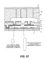
Divots 19 (see, e.g., FIG. 8 or 9A ) may form over the voids or seams 20, on the layer 18 surface, between the wires 14. The voids 20 and divots 19 form due to the spacing between the wires 14, and they can vary depending on the height of the layer 18, as well as the spacing and/or height of the wires 14. These divots 19 can deepen during subsequent processing, such as chemical mechanical processing, as discussed below in regards to FIG. 8 . These divots 19 and seams can oxidize during subsequent processing such as exposure to humid air, an oxidizing ambient photoresist strip, or a plasma oxide deposition and these oxidized silicon regions will not be removed during the final silicon venting or removal step. If this happens, then these oxidized silicon residuals, which are under the MEMS beam, can block the MEMS beam from contacting the lower electrode (wire) 14, resulting in poor actuation. (See, e.g., element 19 a in FIG. 33 .) Tapering the insulator layer 16 profile (FIG. 27C ) reduces or eliminates this effect by eliminating the void and divot, as does eliminating the void by improving the silicon deposition gapfill. The profile can be tapered (FIG. 27C ) by depositing a high density plasma CVD oxide as part or all of the insulator layer 16. Alternatively, an insulator deposition and one or more sputter etch back and subsequent insulator deposition(s) could produce the same tapered profile of the insulator layer 16. Alternatively, as discussed below, the silicon deposition can be modified to taper the silicon profile to 45 degrees by in-situ sputtering the silicon film in the PVD silicon deposition chamber.
The insulator layer 16 over wire 14 also acts to block reaction, alloying, or interdiffusion of the wire 14 material and the layer (cavity material) 18. For example, if wire 14 contains aluminum, then the aluminum can react with the silicon to form an aluminum silicide, which is difficult or impossible to remove during the subsequent layer 18 (sacrificial layer) venting or removal step. This aluminum silicide formation can occur in the upper wire corners, for example, because the insulator layer 16 has a retrograde deposition profile (FIG. 27B ) or has little coverage in the upper wire corner (FIG. 27C ), resulting in exposed aluminum to the layer 18 deposition. Although this problem can be reduced or eliminated by increasing the thickness of the insulator layer, increasing the thickness is not always possible because of the associated reduction in capacitance of the MEMS capacitor formed using wire 14 as a bottom plate. In addition, wire surface or corner defects (not shown) could block the insulator layer 16 from fully coating the aluminum. This aluminum-silicon reaction can result in protruding aluminum silicide whisker-like features that can block or partially block the MEMS beam from actuating. To prevent this layer 16 and 18 reaction, a conformal barrier, such ALD Al2O3 (alumina), ALD Ta2O5 (tantalum pentaoxide), or a combination of both can be deposited. In one exemplary embodiment, layer 16 consists of 80 nm of HDPCVD oxide followed by 15 nm of ALD alumina. ALD films have extremely slow deposition rates and, although they could be used solely as the MEMS capacitor dielectric, it may be impractical because of the long deposition times and high manufacturing costs. One ALD alumina film has a deposition rate of 1 nm per minute, which means that it would take 80 minutes to deposit a 80 nm film. Thus using a combination of fast deposition SiO2 and slow deposition alumina is optimal. Note that the ALD alumina or similar film can be used under the 80 nm of oxide; and also can be used under the upper MEMS electrode 38 to block silicon reaction with the upper MEMS electrode.
In FIG. 3A , an optional processing step of forming a dielectric peg 16 a, (e.g., oxide peg) is shown in accordance with aspects of the invention. In this optional step, the oxide peg 16 a can be formed prior to the formation of the deposition insulator layer 16. For example, the oxide peg 16 a can be a deposited PECVD SiO2 film, which is patterned and etched on the wires 14 using conventional lithographic and etching processes. With this option, the oxide peg 16 a could be patterned and etched first, followed by the wire 14 patterning and etching; or the wire 14 could be patterned and etched first followed by the oxide peg 16 a deposition and etching. Patterning and etching the oxide peg 16 a prior to the wire 14 patterning and etching avoids increasing the aspect ratio 14 a incoming to insulator layer 16 deposition because the oxide between wires 14 is not etched during etching of the oxide peg 16 a. In addition, if the oxide peg 16 a is patterned and etched after the wires 14 are patterned and etched, then the perfluorocarbon-based RIE chemistry used to etch the oxide peg 16 a could also etch the top TiN layer of the wire 14, resulting in a degraded surface and degraded MEMS capacitor electrical yield or reliability. The oxide peg 16 a, when placed over the MEMS actuators in regions away from the MEMS capacitor or contact head, forms a protective layer during MEMS operation, which can prevent the conductor in the MEMS beam from electrically arcing to the lower actuator electrode in areas that the MEMS beam does not need to closely contact the lower electrode. Since the preferred process patterns and etches the oxide peg prior to patterning and etching the wire 14, it is desirable to avoid having the spaces 14 a between the wires 14 intersect the oxide peg. After formation of the oxide peg 16 a, the insulator layer 16 and layer 18 can be formed as described above.
As optional processing steps, the layer 18 can be planarized using, for example, a chemical mechanical polishing (CMP) and then, optionally, additional material (silicon) can be deposited on the polished layer 18 to provide a seamless silicon layer on the surface of the lower silicon MEMS cavity. Note that conventional CMP and subsequent cleaning processes, such as brush cleans, dilute hydrofluoric acid (DHF), buffered hydrofluoric acid (BHF), cryogenic cleans, etc. would be performed after any CMP step to remove the native oxide formed on the silicon surface. For example, referring to FIG. 4A , the layer 18 is deposited on the insulator layer 16 using a conventional deposition process such as, for example, PVD. As shown in FIG. 4A , voids 20 can be formed in the layer 18, between the wires 14, with the divots 19 formed over the voids 20. As shown in FIG. 4B , the layer 18 is planarized using, for example, a CMP process. In FIG. 4C , a second layer of material 22, e.g., silicon, is deposited on the planarized layer 18. In FIG. 4D , the silicon layers 18 and 22 (which form now a single layer (hereinafter referred to as layer 18) are patterned using conventional lithographic and reactive ion etching (RIE) steps. This silicon deposition, CMP, and second deposition process eliminates the divots 19 in the silicon surface, eliminates the chance of oxidizing the seam 20, and partially or completely planarizes the topography on the silicon surface due to the incoming wire 14 and wire space 14 a topography.
One set of example thicknesses would be a 250 nm tall wire 14, a 500 nm space 14 a between wires 14, a 2 micron initial silicon 18 deposition thickness, a 400 nm silicon CMP removal over the wires 14 to planarize the 250 nm step over wires 14, and a subsequent silicon deposition 22 thick enough to partially remain on the wafer during the subsequent reverse oxide planarization processes shown in FIGS. 5-8 . In one exemplary embodiment, 200 nm of silicon is removed from the regions above wires 14 and substantially less than 50 nm in the spaces between wires 14 a, which partially planarizes the regions over the wires 14 and spaces 14 a.
Silicon CMP is commonly performed to form deep trench DRAM capacitors, as known in the art. With this type of silicon CMP, the CMP process is optimized to maximize the selectivity to the pad insulator (e.g. SiO2 or oxide) films on the wafer surface, i.e., the silicon CMP rate is maximized and the oxide CMP rate is minimized such that the selectivity of silicon to oxide is 50:1. This type of silicon CMP process is optimal for silicon films deposited using CVD but can cause problems for silicon films deposited using PVD. PVD silicon films polished with conventional selective silicon CMP processes may have problems with defects in the PVD silicon film which can cause the local polish rate to be reduced. These PVD silicon defects, which may be due to oxidized silicon, other impurities, or the silicon grain structure, can cause the selective silicon CMP process to leave underpolished point defects on the polished silicon surface.
To avoid these point defects during silicon CMP, a less selective or non-selective silicon polish process can be used, e.g., using a SiO2 polish chemistry and process instead of a silicon CMP polish chemistry and process. The use of a less selective silicon polish process eliminates these point surface defects post polish. An example of a selective silicon polish is a basic media, such as TMAH with silica abrasive with a ph high enough to dissolve silicon, i.e., >12, which has a silicon:SiO2 selectivity of 50:1; an example of a non-selective silicon polish is basic media, such as KOH, with a ph<12, which is too low to dissolve the silicon, using a silica abrasive. This non-selective silicon CMP process would have silicon: SiO2 selectivities of less than 50:1 and, in one exemplary embodiment, would be in the range of 2:1 to 1:2.
To avoid polishing into the void 20, it is desirable for the first silicon deposition to be thick enough to bury the void below the surface. Silicon is opaque to optical wave lengths of light. If the subsequent lithographic process used to pattern the silicon uses optical wave lengths, then the silicon CMP process should not fully planarize either alignment structures using the wire level topography; or partially filled alignment structures using the damascene level 12. If the subsequent lithographic processes use infrared light or other methods that can detect features under the silicon, then these precautions are not needed.
A thin native oxide (e.g., SiO2) forms on any silicon surface exposed to air or oxygen, even at room temperature. When the silicon is etched or vented during subsequent processing, the presence of this native oxide can either block the etch or venting, or can remain on the wafer as a few monolayer SiO2 film. To avoid this, either the silicon surface should be hydrogen passivated by exposing the silicon to vapor, plasma, or liquid hydrofluoric acid (HF), or a preclean using, for example, a rf biased argon sputter preclean, should be performed immediately prior to depositing the second silicon layer 22, without exposing the wafer to air or oxygen.
Referring to FIG. 5 , an insulator material (e.g., oxide) 24 is deposited on the layer 18. The oxide deposition can be, for example, a conventional conformal deposition process, depositing the oxide layer 24 to a depth of about approximately the same as the silicon 18 height, e.g., about 2.3 μm for a 2.3 micron thick layer 18. For example, the deposition process can be a 400° C. PECVD oxide deposited using TEOS or silane as a silicon source and oxygen or N2O as an oxygen source, as known in the art. If the oxide layer 24 thickness is intentionally thinner than the height of the silicon layer 18, then the subsequent oxide CMP process shown in FIG. 8 will overpolish and planarize the surface of the silicon layer 18. Conversely, if the oxide layer 24 thickness is intentionally thicker than the height of the silicon layer 18, then the subsequent oxide CMP process shown in FIG. 8 will underpolish the surface of the silicon layer 18 and leave it buried below the oxide surface. Both process options can be desirable, depending on how important minimizing the silicon surface 18 overpolish is vs. planarizing the oxide layer 24 or silicon 18 surface topography from wiring levels 14. In one exemplary embodiment, silicon 18 layer is about 2.3 microns, the oxide layer 24 is about 2.1 microns, and the optional oxide etchback step shown in FIG. 7 is targeted at a full oxide removal, i.e., >2.1 microns. This results in the subsequent oxide polish process further planarizing the silicon layer 18.
In FIG. 6 , an optional reverse etch (reverse damascene process) is performed in accordance with aspects of the invention. More specifically, a resist 26 is deposited on the oxide layer 24 and is patterned to form an opening 28, with the resist edges 26 a overlapping with edges of the underlying layer 18. That is, the resist 26 will slightly mask the underlying layer 18. The overlap needs to be greater than 0 and can be, for example, 3 microns and is minimized to reduce the oxide layer 24 left to be planarized during the subsequent CMP process. If the overlap is negative, then the subsequent RIE etch will etch into the lower portion of oxide layer 24, resulting in a deep trench adjacent to the silicon layer 18, which could cause problems such as residual metal from the subsequent wiring level inside the deep trench, resulting in electrical wire shorting at subsequent levels, and which should be avoided. As shown, the opening is a reverse image of the patterned layer 18.
As shown in FIG. 7 , the oxide material 24 is etched using conventional RIE processes. In embodiments, as shown in FIG. 7 , the etching process results in a “picture frame” 30, which surrounds the underlying layer 18. If the oxide material 24 is etched completely down to the surface of layer 18, then the oxide overpolish in regions away from the layer 18 will be minimized. This can be desirable to minimize the overpolish of layer 18, to reduce its thickness tolerance; and to eliminate the possibility of leaving residual oxide over the silicon in the MEMS capacitor or contact area. Alternatively, some oxide can be left over layer 18, as shown in FIG. 7 .
In FIG. 8 , the oxide material 24 is planarized, e.g., to be planar (e.g., a nearly flat or planar surface) with the underlying layer 18. In embodiments, this process will also planarize the underlying silicon layer 18, which will advantageously result in a planar cavity structure (e.g., having flat or planar surfaces) in subsequent processing steps. The planarization process can be, for example, a CMP process. Unexpectedly, and as discussed in more detail with reference to FIG. 25 , the oxide CMP can minimize the variability of the underlying layer 18; for example, depending on the wiring spacing, the polishing of the oxide material 24 can minimize divots between the wires 14 (e.g., over the space 14 a formed between the wires 14).
The graphs of FIG. 25 show CMP of the oxide layer 24 for 30 seconds, 60 seconds and 90 seconds, with different wiring spacing 14 a of 0.5 μm, 0.8 μm and 5.5 μm. These graphs show the unexpected importance of the wiring spacing 14 a of the wires 14, in order to minimize topography variability of the layer 18. For example, a slot (spacing) of 0.5 μm and a CMP of the oxide for 30 seconds shows a 2 nm divot depth in the layer 18, compared to 5 nm and 10 nm for a CMP of the oxide for 60 seconds and 90 seconds, respectively. Also, a slot of 0.8 μm with a CMP of the oxide for 30 seconds shows a 30 nm divot depth of the layer 18, compared to 2 nm and 8 nm for a CMP of oxide for 60 seconds and 90 seconds, respectively. Additionally, a slot of 5.5 μm with a CMP of the oxide for 30 seconds shows a 170 nm divot depth, compared to 40 nm and 10 nm for a CMP of 60 seconds and 90 seconds, respectively. These results were not expected, as a increasing CMP time of the oxide would have been expected to show an optimization, i.e., reduction of the divot depth, of the topography of the layer 18. These divots in layer 18 will replicate under the MEMS beam, resulting in MEMS beam underside topography. In addition, the MEMS beam underside topography, which will consist of both deposited oxide as well as potentially an oxidized seam under the divot, can have poor adhesion to the MEMS beam with resultant flaking during MEMS operation. This flaking can cause catastrophic MEMS capacitor yield or reliability degradation, due to the presence of flaking oxide in the MEMS cavity under or over the MEMS beam.
Accordingly, a method of reducing a divot depth or the variability of the silicon layer used for a MEMS structure includes determining a spacing between wires formed on the silicon layer. The method further includes etching an oxide layer for a predetermined amount in order to minimize variability of the silicon layer. The etching for a predetermined amount of time, for each spacing, will result in an optimal structure, e.g., reduce any variability in the silicon layer. The divots over layer 18, which form over seams or voids in the silicon due to underlying topography induced by the gap 14 a in layer 14, can be the source of residual oxide under the MEMS beam post venting or release. For example, the oxide layers 24 or 34 can be deposited using a PECVD process which contains an oxidizing plasma and, optionally, at about 350° C. or 400° C., resulting in oxidization of the divot or seam. This oxidized divot or seam CC, as shown in FIG. 33 , can remain on the underside of the MEMS beam post silicon venting, resulting in topography under the MEMS beam, which can either partially block the MEMS beam from contacting the lower capacitor electrode (wire) 14, or disintegrate or fall off during MEMS beam actuation or operation, resulting in dielectric damage of the MEMS capacitor. The optional embodiment described in FIGS. 4B, 4C, and 4D , where the layer 18 is polished and capped with a second silicon layer 22, eliminates this problem.
As an optional step shown in FIG. 9A , the oxide material 24 can be deposited to a thickness of about 3.3 μm, compared to the 2.3 μm shown in FIG. 5 . For this embodiment, the oxide etch depth is similar to the one described in FIG. 7 , but would be approximately 1 um deeper and would need to expose the surface of the underlying silicon layer 18. The divot 19, e.g., may be formed over the voids 20 shown in the layer 18, between the wires 14. As shown in FIG. 9A , the thick oxide material 24 is deposited on the sides of the layer 18, patterned and etched, and polished using CMP. In FIG. 9B , a silicon layer 32, for example, is deposited on the thick oxide material 24 and the layer 18. As mentioned, previously, a native (or any) oxide should be avoided on the surface of layer 18 prior to the deposition of subsequent silicon layer 32 shown in FIG. 9C .
In FIG. 9C , the silicon layer 32 (and portions of the oxide material 24) is planarized using conventional processes such as, for example, CMP, which may eliminate or minimize the divots. In embodiments, this process will advantageously result in a planar cavity structure (e.g., flat or planar surfaces) in subsequent processing steps. These added steps, i.e., silicon deposition, CMP, deposition (FIG. 4A-4C ; FIG. 9A-9C ) and the reverse damascene oxide CMP overpolish (FIG. 6-8 ) or non-reverse damascene oxide CMP overpolish (FIGS. 5 and 8 ) determine both the micro and macro MEMS beam topography. Micro MEMS beam topography due to divots above the silicon voids are further discussed below in relation to FIG. 25 .
An example of undesirable macro topography are curved silicon surfaces 18 a and 18 b shown in FIGS. 9D and 9E . FIG. 9D shows the silicon surface curvature 18 a due to non-optimized planarization, and more specifically shows an example of undesirable macro topography. This macro topography convex 18 a or concave 18 b curvature in the lower sacrificial cavity material 18 can cause released MEMS beam ‘frozen-in’ curvature and poor MEMS actuation, i.e., the MEMS beam can be curved around the sacrificial cavity 18 material, resulting in high post beam release curvature and poor MEMS beam actuation or contact area. The curvature of the silicon surface can be defined by the radius of curvature ROC. A silicon ROC of less than 1 cm is desirable and ROC values greater than 5 cm will result in approximately 50% reduction of MEMS capacitor capacitance due to reduced MEMS capacitor surface contact area and a larger spacing between the two MEMS capacitor plates.
In FIG. 10A , starting from the structure of either FIG. 8 or FIG. 9C , optional trenches 33 can be formed in the silicon layer 18, over wirings 14. To ensure that the silicon is uniformly etched, an optional oxide RIE process can be performed on the resist patterned wafers prior to silicon etch. In addition, with or without the optional oxide RIE process, a HF clean with photoresist on the wafer can be performed to hydrogen passivate the silicon surface prior to etching the silicon. In embodiments, the trenches 33 are formed to a depth of about 0.3 μm into 2 micron tall layer 18 (e.g., sacrificial cavity material 18); although other dimensions are contemplated by the invention depending on the design parameters and, more particularly, the height of the layer 18.
As with the oxide pegs 16 a discussed in FIG. 3A , the purpose of these damascene oxide pegs or trenches 33 is to place a dielectric bumper between the MEMS beam and the lower wire level 14, to prevent electrical arcing due to the close proximity of wires in the MEMS beam and the wire 14 during MEMS operation. Arcing could occur when a high dc voltage, i.e., 5-100V, is applied to the MEMS actuator in, for example, the wire 14. To avoid the potential for electrical arcing, the subsequent MEMS beam metal layer in close contact to the bottom of trench 33 could be removed, as shown in FIGS. 10B and 10C . Oxide peg 33 a has had the subsequent MEMS beam metal layer 38 taken out of the design while oxide peg 33 b has metal layer 38 left in the design.
The subsequent metal layer 38, which is used to form the MEMS beam lower electrode, can be patterned either to cover the oxide peg 33 or to leave it uncovered. If it is uncovered, then the likelihood of arcing or other dielectric damage between the actuator plates is reduced; if it is covered, i.e. metal extends down into oxide peg 33, then the effectiveness of the oxide peg to reduce actuator arcing or dielectric damage may be reduced. If the oxide peg 33 is not covered by metal layer 38 and there is a step down into the peg due to process method chosen, then there may be a thin metal spacer left along the sidewall of the oxide peg. Since this metal spacer does not contact the electrode 38, it is unimportant.
A nearly 90 degree or rounded bottom corner of the oxide peg can be used. To round the peg bottom, which is desirable if the subsequent MEMS beam metal 38 is present over the peg, the rf bias power on the wafer can be reduced or eliminated during the argon-SF6-base silicon etch process and the argon flow can be reduced. The oxide peg 33 can be patterned and etched either before or after the reverse cavity planarization process. If it is done after, then its depth variability is controlled solely by the silicon etch depth variability and not by the reverse cavity oxide CMP planarization step. Alternatively, if it is done before the reverse cavity oxide planarization oxide deposition step, then it will have an added component of height variability, due to CMP removal variability, but it will be filled or partially filled with planarized oxide, which will increase the separation or spacing of subsequent metal level 38 from the actuator metal level 14 if the oxide peg is covered by the metal.
In FIG. 11 , an upper capacitor dielectric or oxide deposition is performed on the structure of FIG. 10A . More specifically, in this deposition step, oxide material 34 can be deposited to a height of about 80 nm; although other dimensions are contemplated by the present invention as discussed previously. The MEMS capacitor dielectric, when the MEMS beam is actuated, comprise dielectric layers 16 and 34, which are separated by a small gap, due to the surface roughness and hillocks of the MEMS capacitor electrodes. A tapered via 36 can be formed in the oxide materials 24 and 34 to the underlying wire 14′. The tapered via 36 can be formed using conventional lithographic, etching, and cleaning processes, known to those of skill in the art. Care should be taken with the tapered via not to overly oxidize the underlying TiN, TiAl3, or AlCu surface, which can cause high via resistance. Optionally, the post via RIE photoresist strip can be performed at low temperature, i.e., 100° C., to minimize oxidization. Alternatively, a damascene tungsten stud via could be fabricated, as is known in the art. The use of a tapered via 36 reduces the CMP exposure of the silicon surface, resulting in less silicon 18 thickness variability, avoiding polishing or damaging the upper MEMS capacitor insulator 34, as well as a lower chance of forming a deep divot. Since the silicon layer 18 thickness determines the pull-in voltage of the MEMS device, minimizing its variability is desirable. Note that the tapered via 36 should be used outside of the silicon cavity area, because the oxide etch used to fabricate it would be blocked by the silicon layer 18 if it was placed inside the silicon cavity. If the subsequent metal deposition process used for wire 38 has poor conformality or side wall coverage, than the aspect ratio of tapered via 36 needs to be low, e.g., 0.5:1. For a 2 micron thick insulator 24, a 4 micron wide tapered via 36 could be used. Alternatively, if a conformal aluminum process, i.e. a hot reflow PVD or CVD process, was used, than a higher aspect ratio could be used for tapered via 36.
In FIG. 12 , a wire of electrode 38 is formed and patterned over the oxide material 34, and also deposited within the via 36 to contact the underlying wire 14′. The electrode 38 can also be deposited in the trenches 33; however, for illustrative purposes the electrode is not shown in the trench 33 of FIG. 12 (although electrode 38 is shown formed in trench in subsequent figures). In embodiments, the electrode 38 can be, for example, AlCu; although other materials are also contemplated by the invention. In embodiments, for example, the electrode 38 can be TiN, TiN or W, Ru, Pt, Jr, amongst other materials. The thicknesses of this and other electrodes and/or wires can vary depending on the specific design parameters. For example, Ti/AlCu/Ti/TiN layers could be used with 10 nm, 480 nm, 10 nm, and 32 nm thickness, respectively, which would form TiAl3 under and over the AlCu after 400 C annealing. To minimize any hillocks, in embodiments, an optional Ti layer may be deposited and/or formed in direct contact with Al, as discussed previously. In this case, the hillocks should be suppressed on the lower surface of the wire (electrode) 38, as opposed to the upper surface. Alternatively, the electrode 38 could be formed from a noble metal, such as Au; or a refractory metal, such as W or Ta; or without a Ti—AlCu interface, e.g., Ti/TiN/AlCu/TiN.
In FIG. 13 , an insulator material 40 is conformally deposited over the electrode 38. In embodiments, the insulator material 40 is a deposited oxide using any of the methods discussed above that is deposited to a height of about 0.5 to 5 μm, depending on the beam spring constant and oxide to metal thickness ratio requirements. In one exemplary embodiment, insulator material is 400° C. PECVD 2 μm oxide and has a well controlled residual stress and thickness. In embodiments, tapered vias 42 are formed in the insulator material 40, to expose portions of the underlying electrode 38 in a fashion similar to the vias 36 formed previously. Alternatively, tungsten stud vias could be fabricated, at the price of degrading the thickness variability of layer 40 due to variable CMP erosion of the insulator layer 40. Variation in the insulator layer 40 thickness or residual stress results in spring constant and stress gradient variability in the overall MEMS beam, which can negatively affect the beam curvature and bending.
As shown in FIG. 14 , an upper electrode 44 is formed and patterned over the insulator layer 40, and also deposited within the vias 42 to contact the lower electrode 38. In embodiments, the upper electrode 44 is formed from the same materials as the lower electrode 38; in one exemplary embodiment, uppers electrode 38 and 44 are composed of Ti/AlCu/Ti/TiN. For tungsten stud vias, the prior art teaches that the uppermost TiN layer should be left on the wires post via etch. For the tapered vias used with these MEMS structures, it may be desirable to fully remove the TiN layer prior to depositing the electrode 38 and 44 metal, i.e., Ti/AlCu/Ti/TiN, by either etching it using a TiN RIE chemistry, sputter it using an argon sputter, or a combination of both to eliminate the potential for via resistance high flyers. In embodiments, the metal volume of the electrodes 38 and 44 should be the same or substantially the same in order to balance the overall volume and stress of the device, and hence not place undue stresses on the beams of the MEM structures. The metal volume is determined by both the metal thickness and the layout. If identical layouts are used for electrodes 38 and 44, then they would have the same volume if their thicknesses were the same. If a slotted or holed layout was used for the lower electrode 38, then the upper electrode would need to be thinned to match the metal volume. In embodiments, the thickness of the lower or upper electrode 44 can be increased or decreased to intentionally place a stress gradient into the beam, which can cause the beam to deflect up or down post release; or to change the beam bending induced by changing temperature, as discussed below. The preceding discussion assumes that the electrodes 38 and 44 are composed of a single, identical metal film. In reality, as discussed above, the electrodes are composed of multiple layers of metal, each with different thermal expansion coefficient (CTE) and other mechanical properties and, if the layout or thickness is varied, it is nearly impossible to exactly match their mechanical properties. If the AlCu portion of the electrodes 38 and 44 is much thicker than the refractory and other metal components, then, to first order, the CTE and other mechanical properties can be approximated by those of the AlCu film.
Alternatively, if the layout of the upper and lower electrodes 38 and 44 are asymmetric or different, then the thickness of the electrode with a lower pattern factor (i.e., less metal) could be thickened to balance the metal volume. One example of an asymmetric upper and lower electrode is shown in FIG. 28 . In this representation, there are diamond (or other patterned shapes) shaped shapes removed from the lower MEMS electrode 200, which are placed to decrease the likelihood of metal hillocks forming. Because the area of lower MEMS electrode 200 is less than the area of upper MEMS electrode 210, the volume of metal in each electrode would be out of balance if the metal thickness for electrodes 200 and 210 were identical. Balancing the metal volume of the lower and upper electrodes is important for both cantilever and bridge MEMS beams because the coefficient of thermal expansion (CTE) of the beam metal, e.g., aluminum, is much greater than the CTE of SiO2.
In embodiments, MEMS electrodes with different areas could be partially balanced. For example, if the lower MEMS beam electrode had 80% less area than the upper MEMS beam electrode, the lower electrode could be thickened by 10% to partially rebalance the metal volume in the two electrodes. Intentionally unbalancing the metal volume in the two MEMS electrodes can cause MEMS beam bending post release or venting which acts to bend the beam up or down into a desirable position; or can minimize the MEMS beam bending over operational use temperature, e.g., −55° C. to 125° C. or any normal range of packaged chip operational temperatures, as discussed below. The MEMS cavity actuation gap is increased or decreased as the MEMS beam bends up or down; and the curvature of the beam, which can reduce the contact area and decrease the capacitance, can change as the MEMS beam expands or contracts with changing temperature. Minimizing the MEMS beam bending over operational chip temperatures is desirable because the actuation voltage is inverse proportional to the MEMS cavity gap.
When the vented MEMS beam movement is constrained by the lid, either because of the lid rivet AA or because the lid is bonded to the lid BB (see, FIG. 31 ), the MEMS beam will not actuate as expected and will be partially or completely non-functional. The regressive lid oxide profile shown in FIG. 16 has the largest regressive extent in the corners of the vias 42 and 48. To reduce this, the vias inside the MEMS cavity 42 and 48 corners can be rounded or chamfered, as shown in FIG. 32 , which reduces the likelihood that the lid oxide will pin the MEMS beam. FIG. 30E shows a non-regressive silicon deposition with tapered side wall profiles for the upper silicon cavity. This conformal silicon deposition process can be obtained, for example, by performing multiple PVD silicon deposition and rf biased wafer etchback steps preferably in-site, i.e. in the same chamber, or ex-situ, i.e., transferring between a deposition and etch back chamber, during the silicon deposition to achieve an approximate 45 degree angled silicon deposition profile. Once the 45 degree angle is achieved, e.g., after about 0.3 μm of net deposition over a 0.3 μm tall feature (FIG. 3 ) or after about 1 μm of net deposition over a much deep feature (FIG. 16 ), the balance of the deposition can consist either of a normal, unbiased, silicon film or a combination of thicker unbiased silicon films with less frequent etch back steps, which may be needed to eliminate an oxidized seam in the silicon due to underlying topography. The goal of these silicon deposition/etch back processes is to both eliminate a regressive overhang structure and also to reduce or eliminate a seam in the deposited silicon due to incoming topography (FIG. 35A ). (This is compared to FIG. 35B which shows an oxide seam to the corner of the MEMs structure.) This non-regressive PVD silicon deposition process combines lower chamber pressure deposition for bottom and sidewall deposition, and uses higher chamber pressure etching, where a rf bias is applied to the wafer, to maximize top surface and corner etching. These steps of low pressure deposition and high pressure etchback are repeated sequentially until a desired thickness is achieved. In one exemplary embodiment, the lower pressure deposition, e.g., <6 MTorr, and high pressure, e.g. >10 mTorr, etchback step thickness values are on the order of 10-50 nm for deposition and 5-25 nm for etching, e.g., the etchbacked silicon removal is less than the deposited thickness, and, as mentioned below, the first silicon layer thickness may be increased to, for example, 50 or 100 nm, to avoid sputtering into the corners of features. In addition, this sequence allows for increased film density on the sidewall and tapered surfaces. The surface area of the Si is then minimized, reducing the amount of surface oxidation. Alternatively, a simultaneous PVD silicon deposition and etchback process could be employed, where the sputtering target is biased to sputter the silicon and the wafer is biased to create 45 degree sidewall angles. This is critical to achieve stable venting performance of the Si as any oxidation reduces the venting rate of the Si cavity.
The desired 45 degree corner angle is obtained by the repeated argon sputter etch back step and, after it is obtained, the silicon deposition process could revert back to a normal deposition process without argon sputter steps. This biased silicon deposition process could also be applied to the lower silicon cavity layer 18 to eliminate voids and seams in the silicon. Care should be taken when sputter etching the silicon during the initial film deposition step to avoid sputtering insulator or other materials from the corners of features. The corner 405 in FIG. 30E could be chamfered to 45 degrees by this in-situ or ex-situ sputtering method, resulting in redeposition of oxide layer 46 into the silicon with resultant difficulty in silicon venting due to the presence of SiO2 in the silicon. To avoid sputtering the exposed corners during the initial silicon deposition, an initial unbiased silicon layer, e.g. 50 or 100 nm, can be deposited.
As the released MEMS beam is heated or cooled, it will bend upwards or downwards due to the electrode with the greater volume of metal expanding or contracting more than the electrode with the lesser volume of metal. FIG. 29 and Table 2 quantitatively show MEMS bridge beam bending versus temperature for beams using the layout shown in FIG. 28 . As mentioned above, the MEMS beam bends because of the CTE mismatch between the oxide and metal in the beam. The dominant metal in the beam, e.g. aluminum, has a yield stress temperature of 150-250° C. The yield stress temperature occurs when the residual stress in the aluminum no longer changes with temperature, as known in the art. At the yield stress temperature, the bending can either flatten out or, more typically, reverse direction (FIG. 29 curve B or E). MEMS bridge beams with balanced metal volume have minimal bending vs. temperature; beams with more upper electrode volume bend upwards with increasing temperature; beams with greater lower electrode volume bend downwards vs. temperature. Note that, if the MEMS bridge beam bending is large enough, the beam will be constrained by the lid over the MEMS beam or the fixed electrode under the MEMS beam (FIG. 29 curves A or F). The most desirable MEMS beam bending vs. temperature behavior is one where the total bending is minimized, for reasons discussed above. This may be achieved using MEMS beam thicknesses such that the MEMS bending profile initially bends upwards and then bends downwards over the temperature range of interest, i.e. FIG. 29 curve C; or vica versa. Achieving a MEMS beam bending curve like this may require intentionally unbalancing the lower and upper electrode volume.
In one exemplary embodiment, the ratio of the lower electrode 38 to upper electrode 44 pattern factor is 0.8:1; the beam oxide is 2 μm thick, the lower electrode has total thickness of 0.56 μm with unreacted AlCu thickness of 450 nm, and the lower electrode has total thickness of 0.48 μm with unreacted AlCu thickness of 370 nm. This combination results in electrodes 38 and 44 with unbalanced volume, i.e., the volume ratio of electrodes 38 and 44 is 0.93:1 and minimized beam bending vs. temperature, over the temperature range of interest qualitatively similar to curve C in FIG. 29 .
| TABLE 2 | ||
| Lower: Upper electrode | ||
| thickness ratio (lower | ||
| electrode is 20% less | Bending at | ||
| than upper electrode | metal yield | ||
| Curve | layout area) | stress point | Comment |
| A | 1:1.5 | +3 um | Upwards bending |
| constrained by lid | |||
| B | 1:1 | +2.2 um | |
| C | 1:0.9 | +0.8 um | |
| D | 1:0.8 | −0.1 um | |
| E | 1:0.7 | −1.0 um | |
| F | 1:0.5 | −2 um | Lower bending |
| constrained by lower | |||
| fixed electrode | |||
This MEMS beam bending post release can cause two problems, as mentioned above:
- a. during normal chip operation, e.g., from about −55° C. to 125° C., MEMS beam bending will increase or decrease the actuation gap resulting in a corresponding change in the actuation voltage; and
- b. if the released MEMS beam is heated to high temperatures (e.g., >150° C., e.g. 400° C.), which is likely due to normal processing after the sacrificial material is vented or removed, then the released MEMS beam will bend upwards, downwards, or both due to thermal expansion mismatch between the upper and lower MEMS beam electrodes and the beam oxide and, if the bending is large enough, be constrained by the lid over the MEMS beam or the fixed electrode under the MEMS beam. Constraining the MEMS beam during annealing can ‘freeze in’ an undesirable curvature, resulting in a MEMS beam that is curved (i.e., not flat). A curved MEMS beam will have reduced contact area, resulting in reduced capacitance. Additionally, if the force exerted by the MEMS beam pressing against either the fixed electrode under the beam or the lid over the beam is too high, then either the MEMS beam or the lid can crack, resulting in catastrophic failure of the MEMS device.
In FIG. 15 , an insulator material 46 is deposited on the upper electrode 44 and exposed portions of the insulator material 40. In embodiments, the insulator material 46 is deposited to a thickness of about 80 nm; although other dimensions are also contemplated by the present invention. To balance the MEMS beam, insulator material 46 over the MEMS beam should be substantially the same thickness as insulator material 34 under the MEMS beam. This thickness balancing of layers 34 and 46 should include any additional dielectric deposition on layer 46 that occurs during the subsequent vent hole dielectric deposition sealing step. A cavity via 48 is formed through the insulator materials, 34, 40 and 46 to the underlying layer 18 by patterning and etching through the insulators. In embodiments, any unwanted oxide, such as a native oxide which is formed by exposing the silicon 18 to air, on the silicon can be cleaned using, for example, an HF acid, prior to the subsequent silicon deposition. It is desirable but not required that the sidewall angle of the cavity via 48 be tapered, to improve the subsequent silicon deposition sidewall coverage and reduce the seam or void in the silicon.
In FIG. 16 , silicon layer 50 is deposited on the structure of FIG. 15 . In embodiments, the silicon layer 50 can be deposited to a thickness of about 4 μm; although other dimensions are also contemplated by the present invention. As shown in FIG. 16 , the silicon layer 50 is deposited such that the topography of the silicon layer 50 changes in accordance with the underlying features. The silicon layer 50 can leave a regressive profile over the vias 42 and 48. During the subsequent oxide deposition, the oxide can fill the regressive structures in a rivet-like fashion so that there is a rivet-shaped oxide peg over the vias 42 and 48. This riveted-shaped oxide feature in the lid can pin the MEMS beam post release. To avoid this MEMS beam pinning, either the silicon layer 50 deposition process needs to be optimized to avoid this shape (FIG. 30E ); or a thick enough silicon 50 layer to pinch off or partially pinch off the via 42 and 48 openings is needed (FIG. 30D ); a silicon deposition, CMP, and subsequent silicon deposition is needed similar to the one discussed for silicon layer 18 previously, or a combination of the above. Also, as shown in FIG. 16 , the silicon layer 50 makes contact with the underlying layer 18 through the via 48. In embodiments, due to the HF acid cleaning, there will be no oxide between the two layers of silicon (e.g., layer 18 and layer 50). In optional embodiments, the silicon layer 50 has a 3 micron initial thickness, undergoes a 1 micron CMP removal, and has a second silicon deposition to achieve the 4 μm thickness.
In an optional embodiment shown in FIG. 17 , the silicon layer 50 can undergo an optional lithographic and RIE process using a reverse mask, similar to that discussed above. This reverse mask would place photoresist over the vias 42 and 48 so that, when the silicon 50 was etched back using a RIE or wet chemical silicon etch process and subsequent resist stripping and cleaning, the topography would be reduced incoming to a subsequent CMP step. The reverse mask shapes need to fully cover the vias 42 and 48 openings, so that trenches would not be etched along their sidewalls, as previously discussed regarding FIG. 6 .
The optional step of FIG. 17 can assist with the subsequent etching/planarization of the silicon layer 50. Note that any CMP or other planarization of the silicon layer 50 cannot completely planarize all features on the wafer if an optical wavelength is used for subsequent lithographic alignment. To avoid complete planarization, the vias 42 and 48 could be stacked in areas outside the functional integrated circuit so that, even if the silicon was planarized over the vias 42 and 48, it would not be planarized over stacked 42 and 48 via structures.
As shown in FIG. 19A , the oxide material 52 can be planarized such that oxide is left over silicon layer 50 (FIG. 19A ), or can be planar with the underlying silicon layer 50, similar to what was previously shown in FIG. 8 . Whether or not the oxide layer 52 is planarized back to the surface of silicon layer 50, additional dielectric may need to be deposited to form the required oxide lid thickness over the MEMS cavity, as discussed below. Alternatively, the oxide layer 52 can be partially planarized, as shown in FIG. 19B ; or left unplanarized. As an optional step much like shown in FIG. 9A , the oxide material can be deposited to a thickness of about 5 μm, compared to the 2.3 μm, with a Si layer, for example, deposited on the thick oxide material. The Si layer (and portions of the oxide material 52) are planarized using conventional processes such as, for example, CMP. The oxide material 52 deposition process should sufficiently fill the wire level 44 spaces such that voids in the oxide do not intersect the CMP planarized oxide surface by, for example, deposition the initial oxide film with HDPCVD oxide to fill the spaces, deposition/etch/deposition oxide, or PECVD TEOS-based oxide, either for the initial oxide deposition or the entire film. With all of these embodiments, the reverse pattern etch back step shown in FIG. 18A is optional.
If silicon layer 50 was not fully planarized, as shown in FIG. 16 , then the oxide layer 52 surface will follow the surface topography of silicon layer 50, as shown in FIG. 19c . With the incoming topography shown in FIG. 19C , the oxide CMP step, with or without the reverse damascene etch back step, could not fully planarize the surface of oxide layer 52 due to the presence of vias 42 and 48, with a resulting profile shown in FIG. 19D . Note that the surface profile shown in FIG. 19D could also have the global profile shown in FIG. 19B superimposed on it.
Alternatively, if the optional oxide etch back step etched down to the silicon surface of silicon layer 50, then the oxide over the vias 42 and 48 would extend below the surface of silicon layer 50. This topography over vias 42 and 48 could result in trenches in the final diced wafer surface, which could cause chip reliability problems due, for example, to water collection in the trenches during humidity-pressure stressing of the packaged chips. To avoid this problem, the oxide layer 52 could be deposited to a thickness such that the openings over vias 42 and 48 pinch off; or the oxide layer 52 could be planarized such that the final surface is planer as in FIG. 19A .
Alternatively, the reverse pattern etchback mask could be modified such that mask openings are removed in areas around the vias 42 and 48. FIG. 19E shows a top view of cavity 50, via 42, and via 48. If a reverse pattern etchback process was used with the vias 42 and 48 blocked (FIG. 19F ), then the oxide would not be etched around vias 42 and 48 (FIG. 19G ) and it would be easier to planarize or substantially planarize the surface of the oxide layer 52. The optional oxide CMP processes used to planarize or partially planarize oxide layer 52 can scratch the surface. An example of a surface scratch RR is shown in FIG. 19H . These surface scratches can act as crack nucleation points after the MEMS sacrificial cavity layers 18 and 50 are vented or removed. To eliminate this problem, an optional second dielectric or oxide deposition is performed, to deposit the layer 400 shown in FIG. 19H .
In FIG. 20 , an oxide material 54, which determines the lid thickness before silicon venting, is shown on the surface. The oxide material 54 can have a thickness before venting of about 3 μm, for example. If the oxide layer 52 had not been removed or fully removed over silicon layer 50, then the total oxide thickness of layers 52 and 54 would determine the lid thickness before silicon venting. In embodiments, a vent hole 58 is patterned, and opened in the oxide lid, exposing a portion of the underlying silicon layer 50. It should be understood that more than one vent hole 58 can be formed in the oxide material 54. The vent hole 58 can be formed using conventional lithographic and etching processes known to those of skill in the art. All of the patterned features discussed in this disclosure are patterned using conventional, e.g. steppers or proximity, lithographic tooling using photomasks, as known in the art. With conventional lithography, extra features on the masks are included to measure feature size, i.e. line width, as well as registration or overlay between the feature currently being imaged and prior level features on the wafer. These extra features are commonly placed in the dicing channel between the active chips, although they can also be placed inside the chips; or active chip features can be used. To match the printed feature to active features inside the active chip, it is important but not required that the prior level features are duplicated. For example, for the vent hole 58, if a structure outside of the active chip is used for measuring feature size or overlay, it should be stacked over the upper silicon cavity 50 and, optionally, the other wires inside the cavity, so that the height off of the wafer and the optical properties (i.e. reflection) of the measured feature are the same as inside the active chip. This is especially important for the vent hole 58 because it has a relatively small width and, depending on the processing used to planarize the upper cavity, the upper cavity can extend 1 μm or more above the surrounding wafer surface, which can cause problems with resist scumming of vent hole 58 printed over the cavity if the vent hole resist width is measured outside of the cavity.
The width and height of the vent hole 58 determines the amount of material that should be deposited after silicon venting to pinch off the vent hole. In general, the amount of material that should be deposited to pinch off the vent hole 58 decreases as the vent hole width decreases; and as the vent hole aspect ratio, which is the ratio of the vent hole height to width, increases. In embodiments, a 3 μm thick pre venting lid would have a 1 μm diameter. In embodiments, the structure, and in particular, the exposed underlying silicon layer 50, can be cleaned with an HF solution prior to venting the silicon. If the vent holes 58 have too high of an aspect ratio or if there are too few vent holes, then it is difficult to vent out the sacrificial cavity material 18 and 50. The vent hole may be circular or nearly circular, to minimize the amount of subsequent material needed to pinch it off. In one exemplary embodiment, the vent hold is shaped in an octagon, which minimized the computational requirement as discussed above.
If the lid is too thin with respect to the MEMS cavity area, either post venting or during any subsequent film deposition, the lid over the evacuated or vented cavities can crack or delaminate due to high film stresses or due to MEMS beam bending up against the lid during annealing. For example, a silicon cavity 500 μm by 500 μm capped with a 1 μm oxide lid would be susceptible to cracking or delaminating after venting or after the subsequent sealing film depositions due to the residual stress of the lid oxide or the sealing films; or because the released MEMS beam pushes up against the lid during annealing. In one exemplary embodiment, approximately 1 micron of oxide lid is required per 10,000 μm2 of cavity area to avoid lid cracking after venting.
In FIG. 21A , the silicon layers 50 and 18 are vented or stripped by way of the vent hole 58. In embodiments, the stripping (e.g., etching) can be performed using a XeF2 etchant through the vent hole 58. The etching will strip all of the material (silicon), forming an upper cavity or chamber 60 a and a lower cavity or chamber 60 b, and is selective to many other materials, including SiO2. As shown in this representation, the upper cavity 60 a and the lower cavity 60 b have planar or nearly planer walls, due to the previous etching steps of the silicon layers 18, 50. An optional HF clean can be performed to remove the native oxide and hydrogen passive the exposed silicon surface prior to venting the silicon.
As shown in FIGS. 21B and 21C , the vent holes 58 can be formed at several locations, to portions (expose portions) of the upper silicon layer 50, the lower layer 18 or both the upper and lower silicon layer 50, 18. For example, as shown in FIG. 21B , the vent holes are formed both inside and outside the cavity vias 48. The vent holes 58 should be either round or nearly round, to minimize the amount of insulator needed to pinch them off post venting. Octagon shapes can be used instead of circles to draw the vent vias, to minimize the computational workload need to process the design data, as discussed above. In this embodiment, the etch rate of the silicon layer 50 in the upper portion 59 a will etch faster than the silicon layer 18 in the lower portion 59 b, thus ensuring that no undue stress is placed on the lower portion 59 b, as shown in FIG. 21d . (The upper portion 59 a and lower portion 59 b will form the upper cavity and lower cavity of the MEMS structure.)
If the vent hole layout is such that the lower cavity 18 vents faster than upper cavity 50, for example by placing the vent holes outside of the vias (cavity vias) 48 as shown in FIG. 21C , then the lower cavity may vent before the upper cavity. This can cause stress-related cracking problems, as shown in FIG. 21C . When the lower cavity layer 18 is almost fully vented but still extends the full height of the cavity and the upper cavity silicon layer 50 is not fully vented and does extend to the full height of the upper cavity, then stress due to lid and beam upwards bending can rip out oxide 60 from the lower cavity as shown in FIG. 21C . For these reasons, it is desirable to place vent holes over the upper cavity such that the upper cavity vents before the lower cavity.
A chamfered lower cavity A and upper B cavity corner 405 is shown in FIG. 21F (also see, e.g., FIG. 21B ). Chamfering the cavity corner can reduce the stress after silicon venting, resulting in reduced chance of dielectric film cracking due to temperature cycling or other stresses. A 45 degree chamfer 405 is shown; although any chamfer angle is envisioned, including a rounded corner (also represented by reference numeral 405). As mentioned previously, chamfering as opposed to rounding corners reduces the computational complexity associated with verifying that the layout does not violate the minimum line and space rules. The vias 42 and 48 inside the cavity can also be chamfered, as discussed below. In FIG. 21C , the vent holes 58 can be formed at several locations, exposing the lower layer 18. In this embodiment, the etch rate of the layer 18 in the lower portion 59 b will be faster than the silicon layer 50 in the upper portion 59 b. The corner of any of the wire levels can also be chamfered, 14, 38, 44, as shown in FIG. 22 to reduce overall stress.
As shown in FIG. 22 , the vent hole 58 can be sealed with a material 62, such as a dielectric or metal. If the sealing material 62 deposits a film inside the cavity on the beam, than it can potentially unbalance the stress of the MEMS beam, and also bond the lid to the beam in regions around vias, as discussed herein and shown by 250 in FIG. 31 . To avoid this problem, in embodiments in which the vent sealing material deposits inside the cavity, the vent holes should be placed far enough away from the vias, e.g., greater than 1 micron or, in an exemplary embodiment, greater than 5 microns, so that released MEMS beam is not bonded to the lid by the vent sealing deposition. Alternatively, the vent holes can be placed in cavity areas away from the MEMS beam, so that no vent hole sealing material is deposited on the released MEMS beam. Optional layer 64 is deposited next to provide a hermetic seal. The layer 64 could be, for example, a 500 nm PECVD silicon nitride film or other films known to provide a hermetic seal over oxide layer 62.
In FIG. 23A , a final via 66 is opened in the structure of FIG. 22 . In embodiments, the via 66 exposes the underlying electrode 44. In embodiments, the via 66 is formed using conventional lithographic and etching processes. In further embodiments, prior to forming the via, an optional polyimide layer 68, for example, can be deposited on the nitride capping layer 64. A problem with forming this final via is its height, which can be in the range of 6-12 μm, due to the planarization of the upper silicon cavity. Long dielectric RIE steps cause problems for RIE tools, due to chamber over heating or other issues; or simply because they have low parts per hour process times and are expensive.
Upper and lower cavities 200 a and 200 b, as previously described herein, can either be the same size or different sizes. The CMP processing used to form the planer lower cavity, show as 200 b, can cause surface curvature on the cavity edge. To avoid this surface curvature from curving the bottom of the MEMS beam, the cavity via 48 should be placed so that the inside edge is beyond the curvature and is over the flat portion of the lower cavity.
In addition, FIG. 24C shows electrical vias 228, which are connected to the lower and upper wire of the cantilever beam. The electrical vias 228 can also be connected to the capacitor arm 220 a, extending between the actuators 215 a. These vias are shown as 42 in FIG. 22 .
Oxide pegs 225 are provided under the beam, and can extend to the capacitor arm 220 a, as well as the actuators 215 a. These oxide pegs 225 could also be above the actuators 215 in FIG. 21B . FIG. 24C also shows oxide pegs 225 under the beam. These oxide pegs are element 33 in FIG. 22 . In operation, electrodes 215 a upon actuation, will cause bending of a MEMS beam. In normal MEMS operation, an actuation voltage is applied between actuators 215 and 215 a. For example, actuator 215 could be grounded and 50V could be applied to actuator 215 a; −25V could be applied to actuator 215 and 25V could be applied to actuator 215 a; 50V could be applied to actuator 215 and actuator 215 a could be grounded; etc. These MEMS layouts have four separate inputs: lower capacitor input, upper capacitor output, lower actuator, and upper actuator. These four electrodes could be combined, as known in the art. For example, the upper actuator 215 a and capacitor 220 a could consist of a single connected wire; the lower actuator 215 and lower capacitor 220 electrode could consist of a single wire; or both. For these simpler 2 or 3 input devices, ac signal and dc actuation would need to be decoupled by, for example, using inductors wired to ground or dc voltages on the electrodes.
In addition, FIG. 24F shows electrical vias 328, which are connected to the lower and upper wire of the cantilever beam. The electrical vias 328 can also be connected to the capacitor arm 320 a. Oxide pegs 325 are provided under the beam, and can extend to the capacitor arm 320 a, as well as the lower actuator 315 c. In operation, the first, second and third actuators (electrodes) 315, upon actuation, will cause bending of a MEMS beam. More specifically, the lower actuator will apply the voltage to the actuators (electrodes).
In both cases the MEMS beam includes metal/insulator/metal with an added thin insulator layer under and over the stack if the MEMS device is a capacitor. One exemplary embodiment would use 0.5 micron lower and upper metal thickness and 2 micron insulator thickness with 80 nm insulator layer over and under the beam if the device was a capacitor. In addition, the actuators 215, (FIGS. 24A-24C ) or actuators 315 (FIGS. 24D-24F ) would be connected to ground, so that, when the actuation voltage is applied to the actuators, the MEMS beam would actuate and bend down, as known in the art. Alternatively, the actuation voltage could be applied to the actuation electrodes in FIGS. 24C and 24F and the actuators in FIGS. 24B and 24C would be grounded. In another embodiment, the actuators and capacitor would be connected together and would need to be grounded using a dc ground, such as an inductor.
In FIGS. 31-33 and 35 an oxide material 54, which determines the lid thickness before silicon venting, is shown on the surface. In embodiments, vent holes 58 are opened in the oxide lid, exposing a portion of the underlying silicon layer 50. It should be understood that more than one vent hole 58 can be formed in the oxide material 54. The vent holes 58 can be formed using conventional lithographic and etching processes known to those of skill in the art. The width and height of the vent holes 58 determine the amount of material that should be deposited after silicon venting to pinch off the vent hole, as discussed in more detail below. The vent holes 58 can be sealed with a material 62, such as a dielectric or metal, as discussed above.
The method as described above is used in the fabrication of integrated circuit chips. The resulting integrated circuit chips can be distributed by the fabricator in raw wafer form (that is, as a single wafer that has multiple unpackaged chips), as a bare die, or in a packaged form. In the latter case the chip is mounted in a single chip package (such as a plastic carrier, with leads that are affixed to a motherboard or other higher level carrier) or in a multichip package (such as a ceramic carrier that has either or both surface interconnections or buried interconnections). In any case the chip is then integrated with other chips, discrete circuit elements, and/or other signal processing devices as part of either (a) an intermediate product, such as a motherboard, or (b) an end product. The end product can be any product that includes integrated circuit chips, ranging from toys and other low-end applications to advanced computer products having a display, a keyboard or other input device, and a central processor.
The terminology used herein is for the purpose of describing particular embodiments only and is not intended to be limiting of the invention. As used herein, the singular forms “a”, “an” and “the” are intended to include the plural forms as well, unless the context clearly indicates otherwise. It will be further understood that the terms “comprises” and/or “comprising,” when used in this specification, specify the presence of stated features, integers, steps, operations, elements, and/or components, but do not preclude the presence or addition of one or more other features, integers, steps, operations, elements, components, and/or groups thereof.
The corresponding structures, materials, acts, and equivalents of all means or step plus function elements in the claims, if applicable, are intended to include any structure, material, or act for performing the function in combination with other claimed elements as specifically claimed. The description of the present invention has been presented for purposes of illustration and description, but is not intended to be exhaustive or limited to the invention in the form disclosed. Many modifications and variations will be apparent to those of ordinary skill in the art without departing from the scope and spirit of the invention. The embodiment was chosen and described in order to best explain the principals of the invention and the practical application, and to enable others of ordinary skill in the art to understand the invention for various embodiments with various modifications as are suited to the particular use contemplated. Accordingly, while the invention has been described in terms of embodiments, those of skill in the art will recognize that the invention can be practiced with modifications and in the spirit and scope of the appended claims.
Claims (13)
1. A Micro-Electro-Mechanical System (MEMS) structure comprising:
a moveable beam comprising at least one insulator layer on a lower electrode such that a volume of the lower electrode is adjusted to modify beam bending characteristics; and
an upper electrode over the at least one insulator layer on top of the lower electrode, wherein
the lower electrode and the upper electrode are composed of Ti/AlCu/Ti/TiN.
2. The MEMS structure of claim 1 , wherein the lower electrode and the upper electrode have identical layouts and same thicknesses.
3. The MEMS structure of claim 1 , wherein one of the lower electrode and the upper electrode is as a slotted or holed layout and one of the upper electrode and the lower electrode, respectively, has a thickness of the slotted or holed layout, to match a metal volume of the lower electrode with a metal volume of the upper electrode.
4. The MEMS structure of claim 1 , wherein the moveable beam is formed from one or more metal layers, comprising a top metal and a bottom metal with an oxide layer therebetween.
5. The MEMS structure of claim 1 , wherein the upper electrode is U-shaped with a via between opposing sides of the upper electrode.
6. The MEMS structure of claim 1 , wherein the lower electrode is in a trench.
7. The MEMS structure of claim 1 , wherein the upper electrode is directly on the at least one insulator layer and is directly on the lower electrode.
8. The MEMS structure of claim 1 , wherein the lower electrode and the upper electrode contacting the lower electrode are different in thicknesses relative to one another, with a metal volume of the upper electrode and the lower electrode being balanced.
9. A Micro-Electro-Mechanical System (MEMS) structure comprising:
a moveable beam comprising at least one insulator layer on a lower electrode such that a volume of the lower electrode is adjusted to modify beam bending characteristics, wherein
the lower electrode and an upper electrode contacting the lower electrode are different in thicknesses relative to one another, with a metal volume of the upper electrode and the lower electrode being balanced.
10. The MEMS structure of claim 9 , wherein one of the lower electrode and the upper electrode is as a slotted or holed layout and one of the upper electrode and the lower electrode, respectively, has a thickness of the slotted or holed layout, to match the metal volume of the lower electrode with the metal volume of the upper electrode.
11. The MEMS structure of claim 9 , wherein the lower electrode is in a trench.
12. The MEMS structure of claim 9 , wherein the upper electrode is directly on the at least one insulator layer and is directly on the lower electrode.
13. The MEMS structure of claim 9 , wherein the upper electrode is U-shaped with a via between opposing sides of the upper electrode.
Priority Applications (4)
| Application Number | Priority Date | Filing Date | Title |
|---|---|---|---|
| US15/437,727 US10011477B2 (en) | 2010-06-25 | 2017-02-21 | Planar cavity MEMS and related structures, methods of manufacture and design structures |
| US15/957,058 US10315913B2 (en) | 2010-06-25 | 2018-04-19 | Planar cavity MEMS and related structures, methods of manufacture and design structures |
| US16/394,138 US10766765B2 (en) | 2010-06-25 | 2019-04-25 | Planar cavity MEMS and related structures, methods of manufacture and design structures |
| US16/587,185 US11111139B2 (en) | 2010-06-25 | 2019-09-30 | Planar cavity MEMS and related structures, methods of manufacture and design structures |
Applications Claiming Priority (5)
| Application Number | Priority Date | Filing Date | Title |
|---|---|---|---|
| US35862110P | 2010-06-25 | 2010-06-25 | |
| US12/973,235 US8709264B2 (en) | 2010-06-25 | 2010-12-20 | Planar cavity MEMS and related structures, methods of manufacture and design structures |
| US14/184,950 US9352954B2 (en) | 2010-06-25 | 2014-02-20 | Planar cavity MEMS and related structures, methods of manufacture and design structures |
| US14/963,892 US9637373B2 (en) | 2010-06-25 | 2015-12-09 | Planar cavity MEMS and related structures, methods of manufacture and design structures |
| US15/437,727 US10011477B2 (en) | 2010-06-25 | 2017-02-21 | Planar cavity MEMS and related structures, methods of manufacture and design structures |
Related Parent Applications (1)
| Application Number | Title | Priority Date | Filing Date |
|---|---|---|---|
| US14/963,892 Continuation US9637373B2 (en) | 2010-06-25 | 2015-12-09 | Planar cavity MEMS and related structures, methods of manufacture and design structures |
Related Child Applications (1)
| Application Number | Title | Priority Date | Filing Date |
|---|---|---|---|
| US15/957,058 Continuation US10315913B2 (en) | 2010-06-25 | 2018-04-19 | Planar cavity MEMS and related structures, methods of manufacture and design structures |
Publications (2)
| Publication Number | Publication Date |
|---|---|
| US20170158490A1 US20170158490A1 (en) | 2017-06-08 |
| US10011477B2 true US10011477B2 (en) | 2018-07-03 |
Family
ID=44627207
Family Applications (45)
| Application Number | Title | Priority Date | Filing Date |
|---|---|---|---|
| US12/973,235 Active 2032-05-04 US8709264B2 (en) | 2010-06-25 | 2010-12-20 | Planar cavity MEMS and related structures, methods of manufacture and design structures |
| US12/973,333 Active 2031-06-08 US8921144B2 (en) | 2010-06-25 | 2010-12-20 | Planar cavity MEMS and related structures, methods of manufacture and design structures |
| US12/973,422 Active 2031-08-06 US8865497B2 (en) | 2010-06-25 | 2010-12-20 | Planar cavity MEMS and related structures, methods of manufacture and design structures |
| US12/973,430 Active 2031-10-25 US8722445B2 (en) | 2010-06-25 | 2010-12-20 | Planar cavity MEMS and related structures, methods of manufacture and design structures |
| US12/973,147 Active 2032-11-19 US8956903B2 (en) | 2010-06-25 | 2010-12-20 | Planar cavity MEMS and related structures, methods of manufacture and design structures |
| US12/973,381 Active US8458888B2 (en) | 2010-06-25 | 2010-12-20 | Method of manufacturing a micro-electro-mechanical system (MEMS) |
| US12/973,285 Active US8685778B2 (en) | 2010-06-25 | 2010-12-20 | Planar cavity MEMS and related structures, methods of manufacture and design structures |
| US12/974,854 Active 2033-11-18 US9406472B2 (en) | 2010-06-25 | 2010-12-21 | Planar cavity MEMS and related structures, methods of manufacture and design structures |
| US12/977,850 Active 2034-07-25 US9330856B2 (en) | 2010-06-25 | 2010-12-23 | Methods of manufacture for micro-electro-mechanical system (MEMS) |
| US13/768,246 Active US9041128B2 (en) | 2010-06-25 | 2013-02-15 | Planar cavity MEMS and related structures, methods of manufacture and design structures |
| US13/868,147 Active 2032-05-26 US9493341B2 (en) | 2010-06-25 | 2013-04-23 | Planar cavity MEMS and related structures, methods of manufacture and design structures |
| US14/184,950 Active US9352954B2 (en) | 2010-06-25 | 2014-02-20 | Planar cavity MEMS and related structures, methods of manufacture and design structures |
| US14/515,681 Active 2032-06-04 US10173889B2 (en) | 2010-06-25 | 2014-10-16 | Planar cavity MEMS and related structures, methods of manufacture and design structures |
| US14/840,422 Active 2031-04-21 US9862598B2 (en) | 2010-06-25 | 2015-08-31 | Planar cavity MEMS and related structures, methods of manufacture and design structures |
| US14/840,434 Active US9764944B2 (en) | 2010-06-25 | 2015-08-31 | Planar cavity MEMS and related structures, methods of manufacture and design structures |
| US14/840,453 Active US9493343B2 (en) | 2010-06-25 | 2015-08-31 | Planar cavity MEMS and related structures, methods of manufacture and design structures |
| US14/963,892 Active US9637373B2 (en) | 2010-06-25 | 2015-12-09 | Planar cavity MEMS and related structures, methods of manufacture and design structures |
| US14/963,844 Active US9828243B2 (en) | 2010-06-25 | 2015-12-09 | Planar cavity MEMS and related structures, methods of manufacture and design structures |
| US14/966,128 Active US9624099B2 (en) | 2010-06-25 | 2015-12-11 | Planar cavity MEMS and related structures, methods of manufacture and design structures |
| US15/148,130 Active US9932225B2 (en) | 2010-06-25 | 2016-05-06 | Planar cavity MEMS and related structures, methods of manufacture and design structures |
| US15/212,888 Active US9815690B2 (en) | 2010-06-25 | 2016-07-18 | Planar cavity MEMS and related structures, methods of manufacture and design structures |
| US15/212,896 Active US9890039B2 (en) | 2010-06-25 | 2016-07-18 | Planar cavity MEMS and related structures, methods of manufacture and design structures |
| US15/215,182 Active US10005661B2 (en) | 2010-06-25 | 2016-07-20 | Planar cavity MEMS and related structures, methods of manufacture and design structures |
| US15/238,854 Active 2031-05-26 US11174160B2 (en) | 2010-06-25 | 2016-08-17 | Planar cavity MEMS and related structures, methods of manufacture and design structures |
| US15/284,868 Active US9926191B2 (en) | 2010-06-25 | 2016-10-04 | Planar cavity MEMS and related structures, methods of manufacture and design structures |
| US15/403,424 Active US10011480B2 (en) | 2010-06-25 | 2017-01-11 | Planar cavity MEMS and related structures, methods of manufacture and design structures |
| US15/437,727 Active US10011477B2 (en) | 2010-06-25 | 2017-02-21 | Planar cavity MEMS and related structures, methods of manufacture and design structures |
| US15/698,682 Active US10308501B2 (en) | 2010-06-25 | 2017-09-08 | Planar cavity MEMS and related structures, methods of manufacture and design structures |
| US15/787,023 Expired - Fee Related US10414646B2 (en) | 2010-06-25 | 2017-10-18 | Planar cavity MEMS and related structures, methods of manufacture and design structures |
| US15/790,515 Active US10093537B2 (en) | 2010-06-25 | 2017-10-23 | Planar cavity MEMS and related structures, methods of manufacture and design structures |
| US15/802,801 Active US10246319B2 (en) | 2010-06-25 | 2017-11-03 | Planar cavity MEMS and related structures, methods of manufacture and design structures |
| US15/802,789 Active US10214416B2 (en) | 2010-06-25 | 2017-11-03 | Planar cavity MEMS and related structures, methods of manufacture and design structures |
| US15/807,715 Active US10081540B2 (en) | 2010-06-25 | 2017-11-09 | Planar cavity MEMS and related structures, methods of manufacture and design structures |
| US15/957,058 Active US10315913B2 (en) | 2010-06-25 | 2018-04-19 | Planar cavity MEMS and related structures, methods of manufacture and design structures |
| US15/973,958 Active US10584026B2 (en) | 2010-06-25 | 2018-05-08 | Planar cavity MEMS and related structures, methods of manufacture and design structures |
| US16/031,132 Active 2032-01-19 US11021364B2 (en) | 2010-06-25 | 2018-07-10 | Planar cavity MEMS and related structures, methods of manufacture and design structures |
| US16/042,303 Active US10618802B2 (en) | 2010-06-25 | 2018-07-23 | Planar cavity MEMS and related structures, methods of manufacture and design structures |
| US16/239,132 Active US10640364B2 (en) | 2010-06-25 | 2019-01-03 | Planar cavity MEMS and related structures, methods of manufacture and design structures |
| US16/270,905 Active US10618803B2 (en) | 2010-06-25 | 2019-02-08 | Planar cavity MEMS and related structures, methods of manufacture and design structures |
| US16/379,982 Active US10640365B2 (en) | 2010-06-25 | 2019-04-10 | Planar cavity MEMS and related structures, methods of manufacture and design structures |
| US16/394,138 Active US10766765B2 (en) | 2010-06-25 | 2019-04-25 | Planar cavity MEMS and related structures, methods of manufacture and design structures |
| US16/448,533 Active US10906803B2 (en) | 2010-06-25 | 2019-06-21 | Planar cavity MEMS and related structures, methods of manufacture and design structures |
| US16/579,983 Active US11111138B2 (en) | 2010-06-25 | 2019-09-24 | Planar cavity mems and related structures, methods of manufacture and design structures |
| US16/580,133 Active US11104572B2 (en) | 2010-06-25 | 2019-09-24 | Planar cavity MEMS and related structures, methods of manufacture and design structures |
| US16/587,185 Active US11111139B2 (en) | 2010-06-25 | 2019-09-30 | Planar cavity MEMS and related structures, methods of manufacture and design structures |
Family Applications Before (26)
| Application Number | Title | Priority Date | Filing Date |
|---|---|---|---|
| US12/973,235 Active 2032-05-04 US8709264B2 (en) | 2010-06-25 | 2010-12-20 | Planar cavity MEMS and related structures, methods of manufacture and design structures |
| US12/973,333 Active 2031-06-08 US8921144B2 (en) | 2010-06-25 | 2010-12-20 | Planar cavity MEMS and related structures, methods of manufacture and design structures |
| US12/973,422 Active 2031-08-06 US8865497B2 (en) | 2010-06-25 | 2010-12-20 | Planar cavity MEMS and related structures, methods of manufacture and design structures |
| US12/973,430 Active 2031-10-25 US8722445B2 (en) | 2010-06-25 | 2010-12-20 | Planar cavity MEMS and related structures, methods of manufacture and design structures |
| US12/973,147 Active 2032-11-19 US8956903B2 (en) | 2010-06-25 | 2010-12-20 | Planar cavity MEMS and related structures, methods of manufacture and design structures |
| US12/973,381 Active US8458888B2 (en) | 2010-06-25 | 2010-12-20 | Method of manufacturing a micro-electro-mechanical system (MEMS) |
| US12/973,285 Active US8685778B2 (en) | 2010-06-25 | 2010-12-20 | Planar cavity MEMS and related structures, methods of manufacture and design structures |
| US12/974,854 Active 2033-11-18 US9406472B2 (en) | 2010-06-25 | 2010-12-21 | Planar cavity MEMS and related structures, methods of manufacture and design structures |
| US12/977,850 Active 2034-07-25 US9330856B2 (en) | 2010-06-25 | 2010-12-23 | Methods of manufacture for micro-electro-mechanical system (MEMS) |
| US13/768,246 Active US9041128B2 (en) | 2010-06-25 | 2013-02-15 | Planar cavity MEMS and related structures, methods of manufacture and design structures |
| US13/868,147 Active 2032-05-26 US9493341B2 (en) | 2010-06-25 | 2013-04-23 | Planar cavity MEMS and related structures, methods of manufacture and design structures |
| US14/184,950 Active US9352954B2 (en) | 2010-06-25 | 2014-02-20 | Planar cavity MEMS and related structures, methods of manufacture and design structures |
| US14/515,681 Active 2032-06-04 US10173889B2 (en) | 2010-06-25 | 2014-10-16 | Planar cavity MEMS and related structures, methods of manufacture and design structures |
| US14/840,422 Active 2031-04-21 US9862598B2 (en) | 2010-06-25 | 2015-08-31 | Planar cavity MEMS and related structures, methods of manufacture and design structures |
| US14/840,434 Active US9764944B2 (en) | 2010-06-25 | 2015-08-31 | Planar cavity MEMS and related structures, methods of manufacture and design structures |
| US14/840,453 Active US9493343B2 (en) | 2010-06-25 | 2015-08-31 | Planar cavity MEMS and related structures, methods of manufacture and design structures |
| US14/963,892 Active US9637373B2 (en) | 2010-06-25 | 2015-12-09 | Planar cavity MEMS and related structures, methods of manufacture and design structures |
| US14/963,844 Active US9828243B2 (en) | 2010-06-25 | 2015-12-09 | Planar cavity MEMS and related structures, methods of manufacture and design structures |
| US14/966,128 Active US9624099B2 (en) | 2010-06-25 | 2015-12-11 | Planar cavity MEMS and related structures, methods of manufacture and design structures |
| US15/148,130 Active US9932225B2 (en) | 2010-06-25 | 2016-05-06 | Planar cavity MEMS and related structures, methods of manufacture and design structures |
| US15/212,888 Active US9815690B2 (en) | 2010-06-25 | 2016-07-18 | Planar cavity MEMS and related structures, methods of manufacture and design structures |
| US15/212,896 Active US9890039B2 (en) | 2010-06-25 | 2016-07-18 | Planar cavity MEMS and related structures, methods of manufacture and design structures |
| US15/215,182 Active US10005661B2 (en) | 2010-06-25 | 2016-07-20 | Planar cavity MEMS and related structures, methods of manufacture and design structures |
| US15/238,854 Active 2031-05-26 US11174160B2 (en) | 2010-06-25 | 2016-08-17 | Planar cavity MEMS and related structures, methods of manufacture and design structures |
| US15/284,868 Active US9926191B2 (en) | 2010-06-25 | 2016-10-04 | Planar cavity MEMS and related structures, methods of manufacture and design structures |
| US15/403,424 Active US10011480B2 (en) | 2010-06-25 | 2017-01-11 | Planar cavity MEMS and related structures, methods of manufacture and design structures |
Family Applications After (18)
| Application Number | Title | Priority Date | Filing Date |
|---|---|---|---|
| US15/698,682 Active US10308501B2 (en) | 2010-06-25 | 2017-09-08 | Planar cavity MEMS and related structures, methods of manufacture and design structures |
| US15/787,023 Expired - Fee Related US10414646B2 (en) | 2010-06-25 | 2017-10-18 | Planar cavity MEMS and related structures, methods of manufacture and design structures |
| US15/790,515 Active US10093537B2 (en) | 2010-06-25 | 2017-10-23 | Planar cavity MEMS and related structures, methods of manufacture and design structures |
| US15/802,801 Active US10246319B2 (en) | 2010-06-25 | 2017-11-03 | Planar cavity MEMS and related structures, methods of manufacture and design structures |
| US15/802,789 Active US10214416B2 (en) | 2010-06-25 | 2017-11-03 | Planar cavity MEMS and related structures, methods of manufacture and design structures |
| US15/807,715 Active US10081540B2 (en) | 2010-06-25 | 2017-11-09 | Planar cavity MEMS and related structures, methods of manufacture and design structures |
| US15/957,058 Active US10315913B2 (en) | 2010-06-25 | 2018-04-19 | Planar cavity MEMS and related structures, methods of manufacture and design structures |
| US15/973,958 Active US10584026B2 (en) | 2010-06-25 | 2018-05-08 | Planar cavity MEMS and related structures, methods of manufacture and design structures |
| US16/031,132 Active 2032-01-19 US11021364B2 (en) | 2010-06-25 | 2018-07-10 | Planar cavity MEMS and related structures, methods of manufacture and design structures |
| US16/042,303 Active US10618802B2 (en) | 2010-06-25 | 2018-07-23 | Planar cavity MEMS and related structures, methods of manufacture and design structures |
| US16/239,132 Active US10640364B2 (en) | 2010-06-25 | 2019-01-03 | Planar cavity MEMS and related structures, methods of manufacture and design structures |
| US16/270,905 Active US10618803B2 (en) | 2010-06-25 | 2019-02-08 | Planar cavity MEMS and related structures, methods of manufacture and design structures |
| US16/379,982 Active US10640365B2 (en) | 2010-06-25 | 2019-04-10 | Planar cavity MEMS and related structures, methods of manufacture and design structures |
| US16/394,138 Active US10766765B2 (en) | 2010-06-25 | 2019-04-25 | Planar cavity MEMS and related structures, methods of manufacture and design structures |
| US16/448,533 Active US10906803B2 (en) | 2010-06-25 | 2019-06-21 | Planar cavity MEMS and related structures, methods of manufacture and design structures |
| US16/579,983 Active US11111138B2 (en) | 2010-06-25 | 2019-09-24 | Planar cavity mems and related structures, methods of manufacture and design structures |
| US16/580,133 Active US11104572B2 (en) | 2010-06-25 | 2019-09-24 | Planar cavity MEMS and related structures, methods of manufacture and design structures |
| US16/587,185 Active US11111139B2 (en) | 2010-06-25 | 2019-09-30 | Planar cavity MEMS and related structures, methods of manufacture and design structures |
Country Status (8)
| Country | Link |
|---|---|
| US (45) | US8709264B2 (en) |
| KR (3) | KR20130039733A (en) |
| CN (8) | CN102906871B (en) |
| CA (2) | CA2787130C (en) |
| DE (5) | DE112011102130B4 (en) |
| GB (6) | GB2494600B (en) |
| TW (3) | TWI549899B (en) |
| WO (5) | WO2011162949A2 (en) |
Cited By (1)
| Publication number | Priority date | Publication date | Assignee | Title |
|---|---|---|---|---|
| US20180009658A1 (en) * | 2010-06-25 | 2018-01-11 | International Business Machines Corporation | Planar cavity mems and related structures, methods of manufacture and design structures |
Families Citing this family (116)
| Publication number | Priority date | Publication date | Assignee | Title |
|---|---|---|---|---|
| US8981876B2 (en) | 2004-11-15 | 2015-03-17 | Avago Technologies General Ip (Singapore) Pte. Ltd. | Piezoelectric resonator structures and electrical filters having frame elements |
| CN102341341B (en) * | 2009-03-04 | 2014-04-30 | Nxp股份有限公司 | MEMS devices |
| US9243316B2 (en) | 2010-01-22 | 2016-01-26 | Avago Technologies General Ip (Singapore) Pte. Ltd. | Method of fabricating piezoelectric material with selected c-axis orientation |
| US8796904B2 (en) | 2011-10-31 | 2014-08-05 | Avago Technologies General Ip (Singapore) Pte. Ltd. | Bulk acoustic resonator comprising piezoelectric layer and inverse piezoelectric layer |
| WO2011114628A1 (en) * | 2010-03-18 | 2011-09-22 | パナソニック株式会社 | Mems element, and manufacturing method of mems element |
| KR101158200B1 (en) * | 2010-06-04 | 2012-06-19 | 삼성전기주식회사 | Optical Image Stabilizer and Method of manufacturing the same |
| CN102275857B (en) * | 2010-06-11 | 2014-04-16 | 上海丽恒光微电子科技有限公司 | Micro-electro-mechanical device and manufacturing method thereof |
| EP2460762B1 (en) * | 2010-12-06 | 2014-10-08 | Nxp B.V. | MEMS device having reduced stiction and manufacturing method |
| FR2970119B1 (en) * | 2010-12-30 | 2013-12-13 | St Microelectronics Crolles 2 Sas | INTEGRATED CIRCUIT CHIP AND METHOD OF MANUFACTURE. |
| FR2970118B1 (en) | 2010-12-30 | 2013-12-13 | St Microelectronics Crolles 2 | INTEGRATED CIRCUIT CHIP AND METHOD OF MANUFACTURE. |
| US8962443B2 (en) * | 2011-01-31 | 2015-02-24 | Avago Technologies General Ip (Singapore) Pte. Ltd. | Semiconductor device having an airbridge and method of fabricating the same |
| US9490771B2 (en) | 2012-10-29 | 2016-11-08 | Avago Technologies General Ip (Singapore) Pte. Ltd. | Acoustic resonator comprising collar and frame |
| US9401692B2 (en) | 2012-10-29 | 2016-07-26 | Avago Technologies General Ip (Singapore) Pte. Ltd. | Acoustic resonator having collar structure |
| US9490418B2 (en) | 2011-03-29 | 2016-11-08 | Avago Technologies General Ip (Singapore) Pte. Ltd. | Acoustic resonator comprising collar and acoustic reflector with temperature compensating layer |
| US8841733B2 (en) * | 2011-05-17 | 2014-09-23 | United Microelectronics Corp. | Semiconductor device and method of fabricating the same |
| US9120667B2 (en) | 2011-06-20 | 2015-09-01 | International Business Machines Corporation | Micro-electro-mechanical system (MEMS) and related actuator bumps, methods of manufacture and design structures |
| US8643140B2 (en) * | 2011-07-11 | 2014-02-04 | United Microelectronics Corp. | Suspended beam for use in MEMS device |
| US8551859B2 (en) * | 2011-11-10 | 2013-10-08 | International Business Machines Corporation | Biosensors integrated with a microfluidic structure |
| US8546240B2 (en) * | 2011-11-11 | 2013-10-01 | International Business Machines Corporation | Methods of manufacturing integrated semiconductor devices with single crystalline beam |
| US8629036B2 (en) | 2011-11-11 | 2014-01-14 | International Business Machines Corporation | Integrated semiconductor devices with amorphous silicon beam, methods of manufacture and design structure |
| US9105751B2 (en) * | 2011-11-11 | 2015-08-11 | International Business Machines Corporation | Integrated semiconductor devices with single crystalline beam, methods of manufacture and design structure |
| US8673670B2 (en) * | 2011-12-15 | 2014-03-18 | International Business Machines Corporation | Micro-electro-mechanical system (MEMS) structures and design structures |
| US8592876B2 (en) * | 2012-01-03 | 2013-11-26 | International Business Machines Corporation | Micro-electro-mechanical system (MEMS) capacitive OHMIC switch and design structures |
| US9093264B2 (en) * | 2012-04-20 | 2015-07-28 | Applied Materials, Inc. | Methods and apparatus for forming silicon passivation layers on germanium or III-V semiconductor devices |
| US9166271B2 (en) * | 2012-06-01 | 2015-10-20 | Purdue Research Foundation | Tunable cavity resonator including a plurality of MEMS beams |
| US9452924B2 (en) | 2012-06-15 | 2016-09-27 | Taiwan Semiconductor Manufacturing Company, Ltd. | MEMS devices and fabrication methods thereof |
| US9450109B2 (en) | 2012-06-15 | 2016-09-20 | Taiwan Semiconductor Manufacturing Company, Ltd. | MEMS devices and fabrication methods thereof |
| US9200973B2 (en) | 2012-06-28 | 2015-12-01 | Intel Corporation | Semiconductor package with air pressure sensor |
| US9102517B2 (en) | 2012-08-22 | 2015-08-11 | International Business Machines Corporation | Semiconductor structures provided within a cavity and related design structures |
| JP2014057125A (en) * | 2012-09-11 | 2014-03-27 | Seiko Epson Corp | Electronic device, method of manufacturing the same, and oscillator |
| US9385684B2 (en) | 2012-10-23 | 2016-07-05 | Avago Technologies General Ip (Singapore) Pte. Ltd. | Acoustic resonator having guard ring |
| JP6247495B2 (en) * | 2012-11-26 | 2017-12-13 | キヤノン株式会社 | Semiconductor device and manufacturing method thereof |
| US9013012B2 (en) * | 2013-03-05 | 2015-04-21 | Stmicroelectronics Pte. Ltd. | Self-sealing membrane for MEMS devices |
| US9573806B2 (en) * | 2013-03-11 | 2017-02-21 | Taiwan Semiconductor Manufacturing Company, Ltd. | MEMS device structure with a capping structure |
| US9102519B2 (en) * | 2013-03-14 | 2015-08-11 | Infineon Technologies Ag | Semiconductor devices and methods of forming thereof |
| US9969613B2 (en) * | 2013-04-12 | 2018-05-15 | International Business Machines Corporation | Method for forming micro-electro-mechanical system (MEMS) beam structure |
| US9059679B2 (en) * | 2013-04-23 | 2015-06-16 | International Business Machines Corporation | Tunable interconnect structures, and integrated circuit containing the same |
| US9419181B2 (en) * | 2013-05-13 | 2016-08-16 | Infineon Technologies Dresden Gmbh | Electrode, an electronic device, and a method for manufacturing an optoelectronic device |
| US10703627B2 (en) | 2013-06-27 | 2020-07-07 | Soitec | Methods of fabricating semiconductor structures including cavities filled with a sacrificial material |
| US8936960B1 (en) * | 2013-07-02 | 2015-01-20 | United Microelectronics Corp. | Method for fabricating an integrated device |
| WO2015042700A1 (en) * | 2013-09-24 | 2015-04-02 | Motion Engine Inc. | Mems components and method of wafer-level manufacturing thereof |
| EP3019442A4 (en) | 2013-07-08 | 2017-01-25 | Motion Engine Inc. | Mems device and method of manufacturing |
| FR3008690B1 (en) * | 2013-07-22 | 2016-12-23 | Commissariat Energie Atomique | DEVICE COMPRISING A FLUID CHANNEL PROVIDED WITH AT LEAST ONE MICRO OR NANOELECTRONIC SYSTEM AND METHOD OF MAKING SUCH A DEVICE |
| ITTO20130651A1 (en) | 2013-07-31 | 2015-02-01 | St Microelectronics Srl | PROCESS OF MANUFACTURING AN ENCAPSULATED DEVICE, IN PARTICULAR AN ENCAPSULATED MICRO-ELECTRO-MECHANICAL SENSOR, EQUIPPED WITH AN ACCESSIBLE STRUCTURE, AS A MEMS MICROPHONE AND ENCAPSULATED DEVICE SO OBTAINED |
| WO2015013828A1 (en) | 2013-08-02 | 2015-02-05 | Motion Engine Inc. | Mems motion sensor and method of manufacturing |
| KR101813905B1 (en) * | 2013-09-27 | 2018-01-02 | 인텔 코포레이션 | An improved arrangement of through-hole structures of a semiconductor package |
| CN103678804A (en) * | 2013-12-11 | 2014-03-26 | 上海工程技术大学 | Method for simulation analysis of MEMS switch |
| JP6590812B2 (en) | 2014-01-09 | 2019-10-16 | モーション・エンジン・インコーポレーテッド | Integrated MEMS system |
| US9385068B2 (en) * | 2014-03-05 | 2016-07-05 | Northrop Grumman Systems Corporation | Stacked interconnect structure and method of making the same |
| WO2015154173A1 (en) | 2014-04-10 | 2015-10-15 | Motion Engine Inc. | Mems pressure sensor |
| US9583294B2 (en) * | 2014-04-25 | 2017-02-28 | Analog Devices Global | MEMS swtich with internal conductive path |
| US9748048B2 (en) | 2014-04-25 | 2017-08-29 | Analog Devices Global | MEMS switch |
| US9384318B2 (en) * | 2014-04-28 | 2016-07-05 | Globalfoundries Inc. | Mask error compensation by optical modeling calibration |
| US11674803B2 (en) | 2014-06-02 | 2023-06-13 | Motion Engine, Inc. | Multi-mass MEMS motion sensor |
| EP3160897A4 (en) * | 2014-06-27 | 2018-01-24 | Intel Corporation | Magnetic nanomechanical devices for stiction compensation |
| US9224858B1 (en) | 2014-07-29 | 2015-12-29 | Globalfoundries Inc. | Lateral double-diffused metal oxide semiconductor field effect transistor (LDMOSFET) with a below source isolation region and a method of forming the LDMOSFET |
| US9446947B2 (en) * | 2014-08-25 | 2016-09-20 | Texas Instruments Incorporated | Use of metal native oxide to control stress gradient and bending moment of a released MEMS structure |
| CN105439080B (en) * | 2014-08-28 | 2017-09-22 | 中芯国际集成电路制造(上海)有限公司 | Mems device and forming method thereof |
| JP6336865B2 (en) * | 2014-09-09 | 2018-06-06 | 日立オートモティブシステムズ株式会社 | Physical quantity sensor |
| US10140407B2 (en) | 2014-11-26 | 2018-11-27 | Taiwan Semiconductor Manufacturing Company, Ltd. | Method, device and computer program product for integrated circuit layout generation |
| WO2016090467A1 (en) | 2014-12-09 | 2016-06-16 | Motion Engine Inc. | 3d mems magnetometer and associated methods |
| US10407299B2 (en) | 2015-01-15 | 2019-09-10 | Motion Engine Inc. | 3D MEMS device with hermetic cavity |
| WO2016126517A1 (en) * | 2015-02-05 | 2016-08-11 | Cavendish Kinetics, Inc | Dvc utilizing mims in the anchor |
| US10103070B2 (en) * | 2015-03-27 | 2018-10-16 | Globalfoundries Inc. | Dynamic integrated circuit fabrication methods |
| US20160289062A1 (en) * | 2015-03-31 | 2016-10-06 | Qualcomm Technologies International, Ltd. | Mems packaging |
| CN107709227A (en) * | 2015-04-21 | 2018-02-16 | 加泰罗尼亚理工大学 | Including the integrated circuit and its preparation method of the multilayer micro mechanical structure for improving q&r with the through hole by using modification |
| JP6569850B2 (en) * | 2015-06-09 | 2019-09-04 | 株式会社村田製作所 | MEMS manufacturing method |
| DE102015212669B4 (en) * | 2015-07-07 | 2018-05-03 | Infineon Technologies Ag | Capacitive microelectromechanical device and method of forming a capacitive microelectromechanical device |
| US9809450B2 (en) * | 2015-08-27 | 2017-11-07 | Invensense, Inc. | CMOS-MEMS integration using metal silicide formation |
| KR20180037238A (en) * | 2015-08-28 | 2018-04-11 | 히타치가세이가부시끼가이샤 | Semiconductor device and manufacturing method thereof |
| US9617142B1 (en) * | 2015-09-30 | 2017-04-11 | Mems Drive, Inc. | MEMS grid for manipulating structural parameters of MEMS devices |
| US9878899B2 (en) | 2015-10-02 | 2018-01-30 | Taiwan Semiconductor Manufacturing Company, Ltd. | Method and apparatus for reducing in-process and in-use stiction for MEMS devices |
| US10338754B2 (en) * | 2015-12-18 | 2019-07-02 | Synaptics Incorporated | Edge-effect mitigation for capacitive sensors |
| CN106904565B (en) * | 2015-12-22 | 2019-06-28 | 中芯国际集成电路制造(上海)有限公司 | A kind of MEMS device and preparation method thereof, electronic device |
| US10784832B2 (en) | 2015-12-28 | 2020-09-22 | Ningbo Semiconductor International Corporation | Film bulk acoustic resonator and method of fabrication same |
| US9741817B2 (en) * | 2016-01-21 | 2017-08-22 | Tower Semiconductor Ltd. | Method for manufacturing a trench metal insulator metal capacitor |
| WO2017134518A1 (en) | 2016-02-04 | 2017-08-10 | Analog Devices Global | Active opening mems switch device |
| US9643838B1 (en) * | 2016-02-05 | 2017-05-09 | Taiwan Semiconductor Manufacturing Company Ltd | Semiconductor device and package and manufacturing method thereof |
| US10770646B2 (en) * | 2016-03-01 | 2020-09-08 | Qualcomm Incorporated | Manufacturing method for flexible PMUT array |
| KR20170133750A (en) * | 2016-05-26 | 2017-12-06 | 삼성전자주식회사 | Computer-implemented method for designing integrated circuit |
| WO2018030045A1 (en) * | 2016-08-08 | 2018-02-15 | 株式会社デンソー | Dynamic quantity sensor and method for manufacturing same |
| JP6555238B2 (en) * | 2016-08-08 | 2019-08-07 | 株式会社デンソー | Mechanical quantity sensor and manufacturing method thereof |
| CN106298371A (en) * | 2016-08-30 | 2017-01-04 | 北京航天微电科技有限公司 | A kind of radio-frequency micro electromechanical switch based on superficial semiconductor technique and preparation method thereof |
| CN106298372A (en) * | 2016-09-07 | 2017-01-04 | 中国科学院微电子研究所 | A kind of micro-nano mechanical switch and manufacture method thereof |
| JP2018046230A (en) * | 2016-09-16 | 2018-03-22 | イビデン株式会社 | Printed Wiring Board |
| JP2018046231A (en) * | 2016-09-16 | 2018-03-22 | イビデン株式会社 | Printed Wiring Board |
| CN107039298B (en) * | 2016-11-04 | 2019-12-24 | 厦门市三安光电科技有限公司 | Transfer device, transfer method, manufacturing method, device and electronic apparatus for micro-component |
| US10322928B2 (en) * | 2016-11-29 | 2019-06-18 | Taiwan Semiconductor Manufacturing Co., Ltd. | Multi-layer sealing film for high seal yield |
| DE102017104109A1 (en) * | 2017-02-28 | 2018-08-30 | Maschinenfabrik Reinhausen Gmbh | Method and device for monitoring capacitor bushings for an AC network |
| US10784833B2 (en) | 2017-04-04 | 2020-09-22 | Vanguard International Semiconductor Singapore Pte. Ltd. | Lamb acoustic wave resonator and filter with self-aligned cavity via |
| US10403674B2 (en) * | 2017-07-12 | 2019-09-03 | Meridian Innovation Pte Ltd | Scalable thermoelectric-based infrared detector |
| FR3070096B1 (en) * | 2017-08-08 | 2021-09-17 | Commissariat Energie Atomique | METHOD OF MANUFACTURING A DETECTION DEVICE WITH TWO SUBSTRATES AND SUCH A DETECTION DEVICE |
| CN107423522A (en) * | 2017-08-14 | 2017-12-01 | 上海工程技术大学 | A kind of method of efficient emulation analysis electromagnetic switch performance |
| DE102017120290B3 (en) | 2017-09-04 | 2018-11-08 | Infineon Technologies Ag | Method for processing a layer structure |
| CN109586680B (en) * | 2017-09-29 | 2021-09-03 | 安华高科技股份有限公司 | Anchored polymer encapsulation for acoustic resonator structures |
| US10650978B2 (en) | 2017-12-15 | 2020-05-12 | Micron Technology, Inc. | Methods of incorporating leaker devices into capacitor configurations to reduce cell disturb |
| WO2019155663A1 (en) * | 2018-02-09 | 2019-08-15 | 株式会社村田製作所 | Mems device |
| WO2019160674A1 (en) * | 2018-02-19 | 2019-08-22 | Applied Materials, Inc. | Pvd titanium dioxide formation using sputter etch to halt onset of crystalinity in thick films |
| US11027967B2 (en) * | 2018-04-09 | 2021-06-08 | Invensense, Inc. | Deformable membrane and a compensating structure thereof |
| CN112262101A (en) | 2018-04-09 | 2021-01-22 | 应美盛股份有限公司 | Environmentally friendly sensing device |
| US10759658B2 (en) | 2018-12-10 | 2020-09-01 | Texas Instruments Incorporated | Hermetic vertical shear weld wafer bonding |
| CN111386000B (en) * | 2018-12-28 | 2021-08-31 | 财团法人工业技术研究院 | Micro-electromechanical heating device |
| CN110171799B (en) * | 2019-05-29 | 2024-04-09 | 苏州知芯传感技术有限公司 | MEMS switch and manufacturing method thereof |
| CN110255489B (en) * | 2019-05-31 | 2022-07-22 | 武汉敏声新技术有限公司 | Three-dimensional monolithic integrated sensor system |
| CN110991069B (en) * | 2019-12-12 | 2023-09-12 | 神华北电胜利能源有限公司 | Boiler efficiency calculating method based on wet oxygen, storage medium and electronic equipment |
| US11365117B2 (en) | 2019-12-23 | 2022-06-21 | Industrial Technology Research Institute | MEMS device and manufacturing method of the same |
| US11939212B2 (en) | 2019-12-23 | 2024-03-26 | Industrial Technology Research Institute | MEMS device, manufacturing method of the same, and integrated MEMS module using the same |
| CN111463530B (en) * | 2020-04-10 | 2022-04-05 | 昆山鸿永微波科技有限公司 | Silicon-based filtering chip with tunable bandwidth |
| CN111591953B (en) * | 2020-05-07 | 2022-08-05 | 南京航空航天大学 | Needle-shaped microelectrode and preparation method thereof |
| CN111517275B (en) * | 2020-05-09 | 2023-06-02 | 中北大学 | Preparation method of practical radio frequency MEMS switch double-layer sacrificial layer |
| CN116390641A (en) * | 2020-06-18 | 2023-07-04 | 中国科学院微电子研究所 | HfO (HfO) 2 Preparation method of base ferroelectric capacitor |
| CN111787474A (en) * | 2020-07-10 | 2020-10-16 | 瑞声科技(南京)有限公司 | MEMS acoustic sensor |
| CN112374456B (en) * | 2020-11-12 | 2024-01-23 | 上海华虹宏力半导体制造有限公司 | Method for manufacturing MEMS device |
| CN113472308B (en) * | 2021-04-29 | 2022-11-22 | 广州乐仪投资有限公司 | Resonator, forming method thereof and electronic equipment |
| CN112977870B (en) * | 2021-05-20 | 2021-09-03 | 成都飞机工业(集团)有限责任公司 | Method for designing riveting inclined riveting clamp of closed angle area of airplane component assembly |
| CN116127887B (en) * | 2023-04-17 | 2023-07-07 | 东南大学 | MEMS device macro model modeling method based on system identification method |
Citations (121)
| Publication number | Priority date | Publication date | Assignee | Title |
|---|---|---|---|---|
| US5278368A (en) | 1991-06-24 | 1994-01-11 | Matsushita Elec. Works, Ltd | Electrostatic relay |
| US5324683A (en) | 1993-06-02 | 1994-06-28 | Motorola, Inc. | Method of forming a semiconductor structure having an air region |
| US5544001A (en) | 1993-01-26 | 1996-08-06 | Matsushita Electric Works, Ltd. | Electrostatic relay |
| US5619061A (en) | 1993-07-27 | 1997-04-08 | Texas Instruments Incorporated | Micromechanical microwave switching |
| US5665657A (en) | 1995-09-18 | 1997-09-09 | Taiwan Semiconductor Manufacturing Company, Ltd | Spin-on-glass partial etchback planarization process |
| US5693568A (en) | 1995-12-14 | 1997-12-02 | Advanced Micro Devices, Inc. | Reverse damascene via structures |
| US5795829A (en) | 1996-06-03 | 1998-08-18 | Advanced Micro Devices, Inc. | Method of high density plasma metal etching |
| WO2000016105A1 (en) | 1998-09-12 | 2000-03-23 | The Secretary Of State For Defence Defence Evaluation And Research Agency | Formation of a bridge in a micro-device |
| US6116863A (en) | 1997-05-30 | 2000-09-12 | University Of Cincinnati | Electromagnetically driven microactuated device and method of making the same |
| US6143638A (en) | 1997-12-31 | 2000-11-07 | Intel Corporation | Passivation structure and its method of fabrication |
| US6160230A (en) | 1999-03-01 | 2000-12-12 | Raytheon Company | Method and apparatus for an improved single pole double throw micro-electrical mechanical switch |
| WO2001098786A1 (en) | 2000-06-21 | 2001-12-27 | Input Output, Inc. | Accelerometer with folded beams |
| US6352917B1 (en) | 2000-06-21 | 2002-03-05 | Chartered Semiconductor Manufacturing Ltd. | Reversed damascene process for multiple level metal interconnects |
| US6359374B1 (en) | 1999-11-23 | 2002-03-19 | Mcnc | Miniature electrical relays using a piezoelectric thin film as an actuating element |
| US20020099980A1 (en) | 2001-01-25 | 2002-07-25 | Olarig Sompong P. | Computer system having configurable core logic chipset for connection to a fault-tolerant accelerated graphics port bus and peripheral component interconnect bus |
| US6445106B1 (en) | 2000-02-18 | 2002-09-03 | Intel Corporation | Micro-electromechanical structure resonator, method of making, and method of using |
| US20020168136A1 (en) | 2001-05-08 | 2002-11-14 | Axsun Technologies, Inc. | Suspended high reflectivity coating on release structure and fabrication process therefor |
| US20030034239A1 (en) | 2001-08-14 | 2003-02-20 | Marc Chason | Micro-electro mechanical system |
| US20030061958A1 (en) | 2001-10-02 | 2003-04-03 | Guobiao Zhang | Low-cost lithography |
| US6573822B2 (en) | 2001-06-18 | 2003-06-03 | Intel Corporation | Tunable inductor using microelectromechanical switches |
| US20030116417A1 (en) | 2001-11-09 | 2003-06-26 | Coventor, Inc. | MEMS device having contact and standoff bumps and related methods |
| US20030148550A1 (en) | 2001-11-07 | 2003-08-07 | International Business Machines Corporation | Method of fabricating micro-electromechanical switches on cmos compatible substrates |
| US6639488B2 (en) | 2001-09-07 | 2003-10-28 | Ibm Corporation | MEMS RF switch with low actuation voltage |
| DE10321482A1 (en) | 2002-05-14 | 2003-11-27 | Denso Corp | Improvement of membrane properties in a semiconductor device with a membrane |
| US20030217915A1 (en) | 2002-05-24 | 2003-11-27 | Luc Ouellet | Fabrication of microstructures with vacuum-sealed cavity |
| US20030229412A1 (en) | 2002-06-07 | 2003-12-11 | David White | Electronic design for integrated circuits based on process related variations |
| EP1382565A1 (en) | 2001-03-29 | 2004-01-21 | Kabushiki Kaisha Toyota Chuo Kenkyusho | Production device and production method for silicon-based structure |
| US20040033639A1 (en) | 2001-05-07 | 2004-02-19 | Applied Materials, Inc. | Integrated method for release and passivation of MEMS structures |
| US6701779B2 (en) | 2002-03-21 | 2004-03-09 | International Business Machines Corporation | Perpendicular torsion micro-electromechanical switch |
| US6713235B1 (en) | 1999-03-30 | 2004-03-30 | Citizen Watch Co., Ltd. | Method for fabricating thin-film substrate and thin-film substrate fabricated by the method |
| US20040126921A1 (en) | 2003-05-09 | 2004-07-01 | Volant Richard P. | Method of fabricating micro-electromechanical switches on cmos compatible substrates |
| US20040150869A1 (en) | 2002-02-19 | 2004-08-05 | Hiroto Kasai | Mems device and methods for manufacturing thereof, light modulation device, glv device and methods for manufacturing thereof, and laser display |
| US6789029B2 (en) | 2002-10-18 | 2004-09-07 | Motorola, Inc. | Method and apparatus for signal extraction in an electronic sensor |
| US20040180541A1 (en) | 2002-01-18 | 2004-09-16 | International Business Machines Corporation | Soft metal conductor and method of making |
| US6808954B2 (en) | 2001-09-07 | 2004-10-26 | Intel Corporation | Vacuum-cavity MEMS resonator |
| US6812814B2 (en) | 2002-07-11 | 2004-11-02 | Intel Corporation | Microelectromechanical (MEMS) switching apparatus |
| US20040235297A1 (en) | 2003-05-23 | 2004-11-25 | Bih-Tiao Lin | Reverse electroplating for damascene conductive region formation |
| US6852926B2 (en) | 2002-03-26 | 2005-02-08 | Intel Corporation | Packaging microelectromechanical structures |
| US20050048687A1 (en) | 2002-07-18 | 2005-03-03 | Svetlana Tatic-Lucic | Recessed electrode for electrostatically actuated structures |
| US20050098840A1 (en) | 2003-11-07 | 2005-05-12 | Matthias Fuertsch | Micromechanical structural element having a diaphragm and method for producing such a structural element |
| US6897537B2 (en) | 2002-06-13 | 2005-05-24 | Wispry, Inc. | Micro-electro-mechanical system (MEMS) variable capacitor apparatuses and related methods |
| US20050124089A1 (en) | 2003-12-08 | 2005-06-09 | Gogoi Bishnu P. | Method of forming a seal for a semiconductor device |
| US6928879B2 (en) | 2003-02-26 | 2005-08-16 | Robert Bosch Gmbh | Episeal pressure sensor and method for making an episeal pressure sensor |
| US20050184836A1 (en) | 2004-02-20 | 2005-08-25 | Chia-Shing Chou | Microelectromechanical device having a common ground plane layer and a set of contact teeth and method for making the same |
| US20050242687A1 (en) | 2004-04-28 | 2005-11-03 | Kabushiki Kaisha Toshiba | Piezoelectric-driven MEMS device and method for manufacturing the same |
| US7002439B2 (en) | 2002-09-16 | 2006-02-21 | Interuniversitair Microelektronica Centrum (Imec) | Switchable capacitor and method of making the same |
| US7008812B1 (en) | 2000-05-30 | 2006-03-07 | Ic Mechanics, Inc. | Manufacture of MEMS structures in sealed cavity using dry-release MEMS device encapsulation |
| US20060055287A1 (en) | 2004-09-16 | 2006-03-16 | Kabushiki Kaisha Toshiba | Piezoelectric actuator and micro-electromechanical device |
| US7019434B2 (en) | 2002-11-08 | 2006-03-28 | Iris Ao, Inc. | Deformable mirror method and apparatus including bimorph flexures and integrated drive |
| US20060065941A1 (en) | 2004-09-28 | 2006-03-30 | Commissariat A L'energie Atomique | Encapsulation component for integrated micro electromechanical systems and fabrication process of the component |
| US7033908B2 (en) | 2003-02-14 | 2006-04-25 | Samsung Electronics Co., Ltd. | Methods of forming integrated circuit devices including insulation layers |
| US7045843B2 (en) | 2003-09-30 | 2006-05-16 | Hitachi, Ltd. | Semiconductor device using MEMS switch |
| US20060108652A1 (en) | 2003-06-04 | 2006-05-25 | Aaron Partridge | Microelectromechanical systems, and methods for encapsulating and fabricating same |
| US20060203421A1 (en) | 2004-12-09 | 2006-09-14 | Morris Arthur S Iii | Micro-electro-mechanical system (MEMS) capacitors, inductors, and related systems and methods |
| US7131105B2 (en) | 2003-09-19 | 2006-10-31 | Coventor, Inc. | System and method for automatic mesh generation from a system-level MEMS design |
| US20070001224A1 (en) | 2005-06-30 | 2007-01-04 | Semiconductor Energy Laboratory Co., Ltd. | Minute structure, micromachine, organic transistor, electric appliance, and manufacturing method thereof |
| US7180145B2 (en) | 2002-12-13 | 2007-02-20 | Wispry, Inc. | Micro-electro-mechanical system (MEMS) variable capacitor apparatuses, systems and related methods |
| US20070048888A1 (en) | 2005-08-29 | 2007-03-01 | Christenson John C | Electrical contact for a MEMS device and method of making |
| US20070090447A1 (en) | 2005-10-25 | 2007-04-26 | Renesas Technology Corp. | Semiconductor device and method of manufacture thereof |
| US20070093045A1 (en) | 2005-10-26 | 2007-04-26 | Semiconductor Energy Laboratory Co., Ltd. | Semiconductor device and manufacturing method thereof |
| US7215229B2 (en) | 2003-09-17 | 2007-05-08 | Schneider Electric Industries Sas | Laminated relays with multiple flexible contacts |
| US20070134927A1 (en) | 2005-07-18 | 2007-06-14 | Dalsa Semiconductor Inc. | Method for removing residues formed during the manufacture of mems devices |
| US20070134835A1 (en) | 2005-12-06 | 2007-06-14 | Hiroshi Fukuda | Switch using micro electro mechanical system |
| US20070138582A1 (en) | 2005-12-20 | 2007-06-21 | Xerox Corporation | Multiple stage MEMS release for isolation of similar materials |
| US20070190680A1 (en) | 2006-02-13 | 2007-08-16 | Hitachi, Ltd. | MEMS device and manufacturing process thereof |
| US7285863B2 (en) | 1999-06-30 | 2007-10-23 | Seiko Epson Corporation | Pad structures including insulating layers having a tapered surface |
| TWI289538B (en) | 2002-09-20 | 2007-11-11 | Iridigm Display Corp | Microelectromechanical systems device and fabricating method thereof |
| US20080001239A1 (en) | 2006-06-29 | 2008-01-03 | Hiroyuki Enomoto | Method for manufacturing semiconductor device and semiconductor device |
| US20080014663A1 (en) | 2005-01-05 | 2008-01-17 | International Business Machines Corporation | Structure and method of fabricating a hinge type mems switch |
| US20080050676A1 (en) | 2006-08-25 | 2008-02-28 | Fujitsu Limited | Semiconductor device manufacturing method, data generating apparatus, data generating method and recording medium readable by computer recoded with data generating program |
| US7344907B2 (en) | 2004-11-19 | 2008-03-18 | International Business Machines Corporation | Apparatus and methods for encapsulating microelectromechanical (MEM) devices on a wafer scale |
| US20080093684A1 (en) | 2006-10-20 | 2008-04-24 | Seiko Epson Corporation | Mems device and fabrication method thereof |
| US20080105951A1 (en) | 2006-11-08 | 2008-05-08 | Seiko Epson Corporation | Electronic Device and Method for Manufacturing Thereof |
| US20080108381A1 (en) | 2005-05-18 | 2008-05-08 | Samsung Electronics Co., Ltd. | Mobile device having display button and method and medium of displaying using the display button |
| US7381583B1 (en) | 2004-05-24 | 2008-06-03 | The United States Of America As Represented By The Secretary Of The Air Force | MEMS RF switch integrated process |
| US7394332B2 (en) | 2005-09-01 | 2008-07-01 | International Business Machines Corporation | Micro-cavity MEMS device and method of fabricating same |
| US7402449B2 (en) | 2005-02-25 | 2008-07-22 | Hitachi, Ltd. | Integrated micro electro-mechanical system and manufacturing method thereof |
| US20080194076A1 (en) | 2007-02-12 | 2008-08-14 | Taiwan Semiconductor Manufacturing Company, Ltd. | Process For Wafer Bonding |
| US20080224319A1 (en) | 2007-03-13 | 2008-09-18 | Oki Electric Industry Co., Ltd. | Micro electro-mechanical system and method of manufacturing the same |
| US20080272867A1 (en) | 2000-11-29 | 2008-11-06 | Microassembly Technologies, Inc. | Mems device with integral packaging |
| US20080308920A1 (en) | 2002-08-07 | 2008-12-18 | Chang-Feng Wan | System and method of fabricating micro cavities |
| US20080315332A1 (en) | 2005-12-15 | 2008-12-25 | Arnd Kaelberer | Micromechanical Component and Manufacturing Method |
| US20090017579A1 (en) | 2007-07-12 | 2009-01-15 | Hitachi, Ltd. | Method of manufacturing micro electro mechanical systems device |
| US20090026892A1 (en) | 2007-01-30 | 2009-01-29 | Taiyo Yuden Co., Ltd. | Micro-cantilever |
| US20090045474A1 (en) | 2007-07-24 | 2009-02-19 | Rohm Co., Ltd. | MEMS sensor and production method of MEMS sensor |
| WO2009050209A2 (en) | 2007-10-15 | 2009-04-23 | Epcos Ag | Manufacturing a mems element having cantilever and cavity on a substrate |
| CN101417785A (en) | 2007-10-24 | 2009-04-29 | 佳世达科技股份有限公司 | Wafer-level sensing element packaging structure and method for producing the same |
| US20090108381A1 (en) | 2001-12-10 | 2009-04-30 | International Business Machines Corporation | Low temperature bi-CMOS compatible process for MEMS RF resonators and filters |
| US20090134513A1 (en) | 2007-07-23 | 2009-05-28 | Jin Qiu | Method and structures for fabricating mems devices on compliant layers |
| US7545081B2 (en) | 2005-11-30 | 2009-06-09 | Samsung Electronics Co., Ltd. | Piezoelectric RF MEMS device and method of fabricating the same |
| US7544531B1 (en) | 2007-03-13 | 2009-06-09 | Sitime Inc. | Ground strap for suppressing stiction during MEMS fabrication |
| US7545622B2 (en) | 2006-03-08 | 2009-06-09 | Wispry, Inc. | Micro-electro-mechanical system (MEMS) variable capacitors and actuation components and related methods |
| US20090146227A1 (en) | 2007-12-06 | 2009-06-11 | Oki Semiconductor Co., Ltd. | Capacitive sensor and manufacturing method therefor |
| US20090145629A1 (en) | 2007-12-05 | 2009-06-11 | Semiconductor Energy Laboratory Co., Ltd. | Micromachine and Method for Manufacturing the Same |
| US20090169035A1 (en) | 2006-03-30 | 2009-07-02 | Pulse Mems Aps | Single Die MEMS Acoustic Transducer and Manufacturing Method |
| US20090218233A1 (en) | 2005-11-18 | 2009-09-03 | Mikael Fredenberg | Method of Forming a Multilayer Structure |
| US20090236114A1 (en) | 2008-03-19 | 2009-09-24 | Susumu Obata | Micromechanical device and method of manufacturing micromechanical device |
| US20090267166A1 (en) | 2008-04-23 | 2009-10-29 | Taiwan Semiconductor Manufacturing Company, Ltd. | Method of manufacturing a device with a cavity |
| US20090275163A1 (en) | 2008-04-30 | 2009-11-05 | Joseph Damian Gordon Lacey | System and Method of Encapsulation |
| US20090325335A1 (en) | 2008-06-23 | 2009-12-31 | Commissariat A L'energie Atomique | Heterogeneous substrate including a sacrificial layer, and a method of fabricating it |
| US20100009509A1 (en) | 2006-01-19 | 2010-01-14 | International Business Machines Corporation | Dual-damascene process to fabricate thick wire structure |
| DE102008040851A1 (en) | 2008-07-30 | 2010-02-04 | Robert Bosch Gmbh | Method for capping a MEMS wafer and MEMS wafer |
| US20100038731A1 (en) | 2005-11-03 | 2010-02-18 | Cavendish Kinetics, Ltd. | Non-volatile memory device |
| US7666700B2 (en) | 2007-03-23 | 2010-02-23 | Oki Semiconductor Co., Ltd. | Method for fabrication MEMS-resonator |
| US20100065930A1 (en) | 2008-09-18 | 2010-03-18 | Rohm Co., Ltd. | Method of etching sacrificial layer, method of manufacturing MEMS device, MEMS device and MEMS sensor |
| US7692519B2 (en) | 2007-12-21 | 2010-04-06 | General Electric Company | MEMS switch with improved standoff voltage control |
| TWI324890B (en) | 2006-12-18 | 2010-05-11 | Advanced Semiconductor Eng | Micro electro-mechanical system device and manufacturing method thereof |
| US20100162821A1 (en) | 2008-12-26 | 2010-07-01 | Yusuke Takeuchi | Mems device and method for fabricating the same |
| US20100181866A1 (en) | 2009-01-19 | 2010-07-22 | Wispry, Inc. | Reduced voltage mems electrostatic actuation methods |
| US20100308423A1 (en) | 2009-06-04 | 2010-12-09 | Kabushiki Kaisha Toshiba | Mems device and manufacturing method thereof |
| US7880246B2 (en) | 2007-11-29 | 2011-02-01 | Stichting Imec Nederland | Microstructure with enlarged mass and electrode area for kinetic to electrical energy conversion |
| US20110049649A1 (en) | 2009-08-27 | 2011-03-03 | International Business Machines Corporation | Integrated circuit switches, design structure and methods of fabricating the same |
| US7923790B1 (en) | 2007-03-09 | 2011-04-12 | Silicon Laboratories Inc. | Planar microshells for vacuum encapsulated devices and damascene method of manufacture |
| US8004053B2 (en) | 2007-10-22 | 2011-08-23 | Kabushiki Kaisha Toshiba | Micromechanical device and method of manufacturing micromechanical device |
| US20110316097A1 (en) | 2010-06-25 | 2011-12-29 | International Business Machines Corporation | Planar cavity mems and related structures, methods of manufacture and design structures |
| US20120031746A1 (en) | 2009-02-06 | 2012-02-09 | Lg Chem, Ltd | Touch screen and manufacturing method thereof |
| US8142669B2 (en) | 2006-02-20 | 2012-03-27 | Sony Corporation | Electromechanical element, electric circuit device and production method of those |
| US20120133006A1 (en) | 2010-11-29 | 2012-05-31 | International Business Machines Corporation | Oxide mems beam |
| US8432240B2 (en) | 2010-07-16 | 2013-04-30 | Telepath Networks, Inc. | Miniature magnetic switch structures |
| US8779886B2 (en) | 2009-11-30 | 2014-07-15 | General Electric Company | Switch structures |
| US8957747B2 (en) | 2010-10-27 | 2015-02-17 | Telepath Networks, Inc. | Multi integrated switching device structures |
Family Cites Families (36)
| Publication number | Priority date | Publication date | Assignee | Title |
|---|---|---|---|---|
| US3004053A (en) | 1958-03-28 | 1961-10-10 | Director Of The Agency Of Ind | Preparation of organosilanes employing alkyl aluminum halides |
| US3956903A (en) | 1975-04-25 | 1976-05-18 | Weil-Mclain Co., Inc. | System for recovering and condensing vapors |
| US6018184A (en) * | 1998-01-22 | 2000-01-25 | Micron Technology, Inc. | Semiconductor structure useful in a self-aligned contact having multiple insulation layers of non-uniform thickness |
| US6473361B1 (en) * | 2000-11-10 | 2002-10-29 | Xerox Corporation | Electromechanical memory cell |
| US20020104990A1 (en) * | 2000-12-19 | 2002-08-08 | Dereus Dana Richard | Across-wafer optical MEMS device and protective lid having across-wafer light-transmissive portions |
| KR100382732B1 (en) * | 2001-01-10 | 2003-05-09 | 삼성전자주식회사 | Method for fabricating cylinder-type capacitor of semiconductor device |
| US6780759B2 (en) * | 2001-05-09 | 2004-08-24 | Silicon Genesis Corporation | Method for multi-frequency bonding |
| US7033910B2 (en) * | 2001-09-12 | 2006-04-25 | Reveo, Inc. | Method of fabricating multi layer MEMS and microfluidic devices |
| US6930364B2 (en) * | 2001-09-13 | 2005-08-16 | Silicon Light Machines Corporation | Microelectronic mechanical system and methods |
| CN1229860C (en) * | 2002-04-30 | 2005-11-30 | 中芯国际集成电路制造(上海)有限公司 | Hollow-groove isolation object and making method thereof |
| JP4864307B2 (en) | 2003-09-30 | 2012-02-01 | アイメック | Method for selectively forming an air gap and apparatus obtained by the method |
| KR100541657B1 (en) * | 2004-06-29 | 2006-01-11 | 삼성전자주식회사 | Multi-gate transistor fabrication method and multi-gate transistor fabricated thereby |
| US20060067650A1 (en) * | 2004-09-27 | 2006-03-30 | Clarence Chui | Method of making a reflective display device using thin film transistor production techniques |
| JP4907544B2 (en) * | 2004-10-27 | 2012-03-28 | エプコス アクチエンゲゼルシャフト | Electronic devices |
| DE102004061796A1 (en) * | 2004-12-22 | 2006-07-13 | Robert Bosch Gmbh | Micromechanical capacitive sensor element |
| US7417287B2 (en) | 2005-07-01 | 2008-08-26 | System General Corp. | Electrostatic discharge device having controllable trigger voltage |
| US7877866B1 (en) * | 2005-10-26 | 2011-02-01 | Second Sight Medical Products, Inc. | Flexible circuit electrode array and method of manufacturing the same |
| FR2898597B1 (en) * | 2006-03-16 | 2008-09-19 | Commissariat Energie Atomique | ENCAPSULATION IN A HERMETIC CAVITY OF A MICROELECTRONIC COMPOUND, IN PARTICULAR A MEMS |
| GB0605576D0 (en) * | 2006-03-20 | 2006-04-26 | Oligon Ltd | MEMS device |
| US20080160749A1 (en) * | 2006-12-27 | 2008-07-03 | Texas Instruments Incorporated | Semiconductor device and method of forming thereof |
| KR20090125087A (en) * | 2007-02-20 | 2009-12-03 | 퀄컴 엠이엠스 테크놀로지스, 인크. | Equipment and methods for etching of mems |
| CN101261963B (en) * | 2007-03-08 | 2010-12-29 | 诚佑科技股份有限公司 | Miniature electronic part and making method |
| CN101267689A (en) * | 2007-03-14 | 2008-09-17 | 佳乐电子股份有限公司 | Capacitor micro microphone chip |
| US20090013449A1 (en) * | 2007-07-10 | 2009-01-15 | Colleen Kahn | Pacifier securing device |
| CN101434376B (en) * | 2007-11-16 | 2011-10-19 | 微智半导体股份有限公司 | Method for manufacturing suspension micro electromechanical structure |
| EP2107038B1 (en) * | 2008-03-31 | 2012-05-16 | Imec | Electrostatically actuatable MEMS device featuring reduced substrate charging |
| WO2009133506A2 (en) * | 2008-04-29 | 2009-11-05 | Nxp B.V. | Mems device and manufacturing method |
| WO2010006065A2 (en) * | 2008-07-08 | 2010-01-14 | Wispry, Inc. | Thin-film lid mems devices and methods |
| JP2010021187A (en) * | 2008-07-08 | 2010-01-28 | Nec Electronics Corp | Method of designing semiconductor integrated circuit, design program, and method of manufacturing semiconductor integrated circuit |
| US8957485B2 (en) * | 2009-01-21 | 2015-02-17 | Cavendish Kinetics, Ltd. | Fabrication of MEMS based cantilever switches by employing a split layer cantilever deposition scheme |
| ES2342872B1 (en) | 2009-05-20 | 2011-05-30 | Baolab Microsystems S.L. | CHIP THAT INCLUDES A MEMS PROVIDED IN AN INTEGRATED CIRCUIT AND CORRESPONDING MANUFACTURING PROCEDURE. |
| US8692364B2 (en) * | 2009-08-07 | 2014-04-08 | Nec Corporation | Semiconductor device and method for manufacturing the same |
| CN102348155B (en) | 2010-07-30 | 2014-02-05 | 上海丽恒光微电子科技有限公司 | Micro-electromechanical microphone and manufacturing method thereof |
| US8138008B1 (en) | 2010-11-29 | 2012-03-20 | International Business Machines Corporation | Forming an oxide MEMS beam |
| JP2014200857A (en) * | 2013-04-01 | 2014-10-27 | 株式会社東芝 | Mems device and manufacturing method of the same |
| US10414046B1 (en) | 2016-11-07 | 2019-09-17 | X Development Llc | Modular robot design |
-
2010
- 2010-12-20 US US12/973,235 patent/US8709264B2/en active Active
- 2010-12-20 US US12/973,333 patent/US8921144B2/en active Active
- 2010-12-20 US US12/973,422 patent/US8865497B2/en active Active
- 2010-12-20 US US12/973,430 patent/US8722445B2/en active Active
- 2010-12-20 US US12/973,147 patent/US8956903B2/en active Active
- 2010-12-20 US US12/973,381 patent/US8458888B2/en active Active
- 2010-12-20 US US12/973,285 patent/US8685778B2/en active Active
- 2010-12-21 US US12/974,854 patent/US9406472B2/en active Active
- 2010-12-23 US US12/977,850 patent/US9330856B2/en active Active
-
2011
- 2011-06-08 GB GB1300265.4A patent/GB2494600B/en not_active Expired - Fee Related
- 2011-06-08 DE DE112011102130.5T patent/DE112011102130B4/en active Active
- 2011-06-08 DE DE112011102135.6T patent/DE112011102135B4/en active Active
- 2011-06-08 WO PCT/US2011/039560 patent/WO2011162949A2/en active Application Filing
- 2011-06-08 CN CN201180025549.0A patent/CN102906871B/en active Active
- 2011-06-08 CN CN201180025546.7A patent/CN102906009B/en active Active
- 2011-06-08 WO PCT/US2011/039571 patent/WO2011162953A2/en active Application Filing
- 2011-06-08 KR KR1020127030991A patent/KR20130039733A/en not_active Application Discontinuation
- 2011-06-08 GB GB1300085.6A patent/GB2494359B/en not_active Expired - Fee Related
- 2011-06-08 KR KR1020127031138A patent/KR20130020685A/en not_active Application Discontinuation
- 2011-06-08 CN CN201180025550.3A patent/CN102906010B/en active Active
- 2011-06-08 GB GB1300091.4A patent/GB2494360B/en active Active
- 2011-06-08 DE DE112011102134.8T patent/DE112011102134B4/en active Active
- 2011-06-08 KR KR1020127033926A patent/KR101800914B1/en active IP Right Grant
- 2011-06-08 WO PCT/US2011/039564 patent/WO2011162950A2/en active Application Filing
- 2011-06-15 DE DE112011102136.4T patent/DE112011102136B4/en active Active
- 2011-06-15 CN CN201180025545.2A patent/CN102906008B/en active Active
- 2011-06-15 DE DE112011102124.0T patent/DE112011102124B4/en active Active
- 2011-06-15 CN CN201180025557.5A patent/CN102906011B/en active Active
- 2011-06-15 WO PCT/EP2011/059881 patent/WO2011160986A1/en active Application Filing
- 2011-06-15 CA CA2787130A patent/CA2787130C/en active Active
- 2011-06-15 GB GB1300040.1A patent/GB2494824B/en active Active
- 2011-06-15 CA CA2787161A patent/CA2787161A1/en not_active Abandoned
- 2011-06-15 GB GB1300041.9A patent/GB2494355B/en not_active Expired - Fee Related
- 2011-06-15 WO PCT/EP2011/059880 patent/WO2011160985A2/en active Application Filing
- 2011-06-24 CN CN201110173720.4A patent/CN102295263B/en active Active
- 2011-06-24 TW TW100122287A patent/TWI549899B/en active
- 2011-06-24 CN CN201110174027.9A patent/CN102295264B/en active Active
- 2011-06-24 TW TW100122300A patent/TWI538873B/en not_active IP Right Cessation
- 2011-06-24 CN CN201110174587.4A patent/CN102295265B/en active Active
- 2011-06-24 TW TW100122295A patent/TWI537204B/en active
-
2013
- 2013-02-15 US US13/768,246 patent/US9041128B2/en active Active
- 2013-04-23 US US13/868,147 patent/US9493341B2/en active Active
-
2014
- 2014-02-20 US US14/184,950 patent/US9352954B2/en active Active
- 2014-10-16 US US14/515,681 patent/US10173889B2/en active Active
- 2014-10-23 GB GBGB1418872.6A patent/GB201418872D0/en not_active Ceased
-
2015
- 2015-08-31 US US14/840,422 patent/US9862598B2/en active Active
- 2015-08-31 US US14/840,434 patent/US9764944B2/en active Active
- 2015-08-31 US US14/840,453 patent/US9493343B2/en active Active
- 2015-12-09 US US14/963,892 patent/US9637373B2/en active Active
- 2015-12-09 US US14/963,844 patent/US9828243B2/en active Active
- 2015-12-11 US US14/966,128 patent/US9624099B2/en active Active
-
2016
- 2016-05-06 US US15/148,130 patent/US9932225B2/en active Active
- 2016-07-18 US US15/212,888 patent/US9815690B2/en active Active
- 2016-07-18 US US15/212,896 patent/US9890039B2/en active Active
- 2016-07-20 US US15/215,182 patent/US10005661B2/en active Active
- 2016-08-17 US US15/238,854 patent/US11174160B2/en active Active
- 2016-10-04 US US15/284,868 patent/US9926191B2/en active Active
-
2017
- 2017-01-11 US US15/403,424 patent/US10011480B2/en active Active
- 2017-02-21 US US15/437,727 patent/US10011477B2/en active Active
- 2017-09-08 US US15/698,682 patent/US10308501B2/en active Active
- 2017-10-18 US US15/787,023 patent/US10414646B2/en not_active Expired - Fee Related
- 2017-10-23 US US15/790,515 patent/US10093537B2/en active Active
- 2017-11-03 US US15/802,801 patent/US10246319B2/en active Active
- 2017-11-03 US US15/802,789 patent/US10214416B2/en active Active
- 2017-11-09 US US15/807,715 patent/US10081540B2/en active Active
-
2018
- 2018-04-19 US US15/957,058 patent/US10315913B2/en active Active
- 2018-05-08 US US15/973,958 patent/US10584026B2/en active Active
- 2018-07-10 US US16/031,132 patent/US11021364B2/en active Active
- 2018-07-23 US US16/042,303 patent/US10618802B2/en active Active
-
2019
- 2019-01-03 US US16/239,132 patent/US10640364B2/en active Active
- 2019-02-08 US US16/270,905 patent/US10618803B2/en active Active
- 2019-04-10 US US16/379,982 patent/US10640365B2/en active Active
- 2019-04-25 US US16/394,138 patent/US10766765B2/en active Active
- 2019-06-21 US US16/448,533 patent/US10906803B2/en active Active
- 2019-09-24 US US16/579,983 patent/US11111138B2/en active Active
- 2019-09-24 US US16/580,133 patent/US11104572B2/en active Active
- 2019-09-30 US US16/587,185 patent/US11111139B2/en active Active
Patent Citations (163)
| Publication number | Priority date | Publication date | Assignee | Title |
|---|---|---|---|---|
| US5278368A (en) | 1991-06-24 | 1994-01-11 | Matsushita Elec. Works, Ltd | Electrostatic relay |
| US5544001A (en) | 1993-01-26 | 1996-08-06 | Matsushita Electric Works, Ltd. | Electrostatic relay |
| US5324683A (en) | 1993-06-02 | 1994-06-28 | Motorola, Inc. | Method of forming a semiconductor structure having an air region |
| US5619061A (en) | 1993-07-27 | 1997-04-08 | Texas Instruments Incorporated | Micromechanical microwave switching |
| US5665657A (en) | 1995-09-18 | 1997-09-09 | Taiwan Semiconductor Manufacturing Company, Ltd | Spin-on-glass partial etchback planarization process |
| US5693568A (en) | 1995-12-14 | 1997-12-02 | Advanced Micro Devices, Inc. | Reverse damascene via structures |
| US5795829A (en) | 1996-06-03 | 1998-08-18 | Advanced Micro Devices, Inc. | Method of high density plasma metal etching |
| US6116863A (en) | 1997-05-30 | 2000-09-12 | University Of Cincinnati | Electromagnetically driven microactuated device and method of making the same |
| US6143638A (en) | 1997-12-31 | 2000-11-07 | Intel Corporation | Passivation structure and its method of fabrication |
| WO2000016105A1 (en) | 1998-09-12 | 2000-03-23 | The Secretary Of State For Defence Defence Evaluation And Research Agency | Formation of a bridge in a micro-device |
| US6160230A (en) | 1999-03-01 | 2000-12-12 | Raytheon Company | Method and apparatus for an improved single pole double throw micro-electrical mechanical switch |
| US6713235B1 (en) | 1999-03-30 | 2004-03-30 | Citizen Watch Co., Ltd. | Method for fabricating thin-film substrate and thin-film substrate fabricated by the method |
| US7285863B2 (en) | 1999-06-30 | 2007-10-23 | Seiko Epson Corporation | Pad structures including insulating layers having a tapered surface |
| US6359374B1 (en) | 1999-11-23 | 2002-03-19 | Mcnc | Miniature electrical relays using a piezoelectric thin film as an actuating element |
| US6445106B1 (en) | 2000-02-18 | 2002-09-03 | Intel Corporation | Micro-electromechanical structure resonator, method of making, and method of using |
| US7008812B1 (en) | 2000-05-30 | 2006-03-07 | Ic Mechanics, Inc. | Manufacture of MEMS structures in sealed cavity using dry-release MEMS device encapsulation |
| WO2001098786A1 (en) | 2000-06-21 | 2001-12-27 | Input Output, Inc. | Accelerometer with folded beams |
| US6352917B1 (en) | 2000-06-21 | 2002-03-05 | Chartered Semiconductor Manufacturing Ltd. | Reversed damascene process for multiple level metal interconnects |
| US20080272867A1 (en) | 2000-11-29 | 2008-11-06 | Microassembly Technologies, Inc. | Mems device with integral packaging |
| US20020099980A1 (en) | 2001-01-25 | 2002-07-25 | Olarig Sompong P. | Computer system having configurable core logic chipset for connection to a fault-tolerant accelerated graphics port bus and peripheral component interconnect bus |
| US20080257497A1 (en) | 2001-03-29 | 2008-10-23 | Kabushiki Kaisha Toyota Chuo Kenkyusho | Device for manufacturing a silicon structure, and manufacturing method thereof |
| EP1382565A1 (en) | 2001-03-29 | 2004-01-21 | Kabushiki Kaisha Toyota Chuo Kenkyusho | Production device and production method for silicon-based structure |
| US20040094086A1 (en) | 2001-03-29 | 2004-05-20 | Keiichi Shimaoka | Production device and production method for silicon-based structure |
| US20040033639A1 (en) | 2001-05-07 | 2004-02-19 | Applied Materials, Inc. | Integrated method for release and passivation of MEMS structures |
| US20020168136A1 (en) | 2001-05-08 | 2002-11-14 | Axsun Technologies, Inc. | Suspended high reflectivity coating on release structure and fabrication process therefor |
| US6573822B2 (en) | 2001-06-18 | 2003-06-03 | Intel Corporation | Tunable inductor using microelectromechanical switches |
| US20030034239A1 (en) | 2001-08-14 | 2003-02-20 | Marc Chason | Micro-electro mechanical system |
| US6639488B2 (en) | 2001-09-07 | 2003-10-28 | Ibm Corporation | MEMS RF switch with low actuation voltage |
| US6808954B2 (en) | 2001-09-07 | 2004-10-26 | Intel Corporation | Vacuum-cavity MEMS resonator |
| US20050036269A1 (en) | 2001-09-07 | 2005-02-17 | Intel Corporation | Vacuum-cavity MEMS resonator |
| US20030061958A1 (en) | 2001-10-02 | 2003-04-03 | Guobiao Zhang | Low-cost lithography |
| US20030148550A1 (en) | 2001-11-07 | 2003-08-07 | International Business Machines Corporation | Method of fabricating micro-electromechanical switches on cmos compatible substrates |
| US6847114B2 (en) | 2001-11-09 | 2005-01-25 | Turnstone Systems, Inc. | Micro-scale interconnect device with internal heat spreader and method for fabricating same |
| US6746891B2 (en) | 2001-11-09 | 2004-06-08 | Turnstone Systems, Inc. | Trilayered beam MEMS device and related methods |
| US20030116417A1 (en) | 2001-11-09 | 2003-06-26 | Coventor, Inc. | MEMS device having contact and standoff bumps and related methods |
| US6882264B2 (en) | 2001-11-09 | 2005-04-19 | Wispry, Inc. | Electrothermal self-latching MEMS switch and method |
| US6917086B2 (en) | 2001-11-09 | 2005-07-12 | Turnstone Systems, Inc. | Trilayered beam MEMS device and related methods |
| DE60215045T2 (en) | 2001-11-09 | 2007-03-29 | Wispry, Inc. | THREE-LINE BEAM MEMS DEVICE AND METHOD THEREFOR |
| US6876482B2 (en) | 2001-11-09 | 2005-04-05 | Turnstone Systems, Inc. | MEMS device having contact and standoff bumps and related methods |
| DE60222468T2 (en) | 2001-11-09 | 2008-06-12 | Wispry, Inc. | MEMS DEVICE WITH THREE-LINE BENDING BAR AND METHOD THEREFOR |
| US6876047B2 (en) | 2001-11-09 | 2005-04-05 | Turnstone Systems, Inc. | MEMS device having a trilayered beam and related methods |
| US20090108381A1 (en) | 2001-12-10 | 2009-04-30 | International Business Machines Corporation | Low temperature bi-CMOS compatible process for MEMS RF resonators and filters |
| US20040180541A1 (en) | 2002-01-18 | 2004-09-16 | International Business Machines Corporation | Soft metal conductor and method of making |
| US20040150869A1 (en) | 2002-02-19 | 2004-08-05 | Hiroto Kasai | Mems device and methods for manufacturing thereof, light modulation device, glv device and methods for manufacturing thereof, and laser display |
| US6701779B2 (en) | 2002-03-21 | 2004-03-09 | International Business Machines Corporation | Perpendicular torsion micro-electromechanical switch |
| US6852926B2 (en) | 2002-03-26 | 2005-02-08 | Intel Corporation | Packaging microelectromechanical structures |
| DE10321482A1 (en) | 2002-05-14 | 2003-11-27 | Denso Corp | Improvement of membrane properties in a semiconductor device with a membrane |
| US20030217915A1 (en) | 2002-05-24 | 2003-11-27 | Luc Ouellet | Fabrication of microstructures with vacuum-sealed cavity |
| US20030229412A1 (en) | 2002-06-07 | 2003-12-11 | David White | Electronic design for integrated circuits based on process related variations |
| US6897537B2 (en) | 2002-06-13 | 2005-05-24 | Wispry, Inc. | Micro-electro-mechanical system (MEMS) variable capacitor apparatuses and related methods |
| US6812814B2 (en) | 2002-07-11 | 2004-11-02 | Intel Corporation | Microelectromechanical (MEMS) switching apparatus |
| US20050048687A1 (en) | 2002-07-18 | 2005-03-03 | Svetlana Tatic-Lucic | Recessed electrode for electrostatically actuated structures |
| US7299538B2 (en) | 2002-07-18 | 2007-11-27 | Wispry, Inc. | Method for fabricating micro-electro-mechanical systems |
| US7064637B2 (en) | 2002-07-18 | 2006-06-20 | Wispry, Inc. | Recessed electrode for electrostatically actuated structures |
| US20080308920A1 (en) | 2002-08-07 | 2008-12-18 | Chang-Feng Wan | System and method of fabricating micro cavities |
| US7579663B2 (en) | 2002-08-07 | 2009-08-25 | Chang-Feng Wan | Hermetic packaging and method of manufacture and use therefore |
| US7002439B2 (en) | 2002-09-16 | 2006-02-21 | Interuniversitair Microelektronica Centrum (Imec) | Switchable capacitor and method of making the same |
| TWI289538B (en) | 2002-09-20 | 2007-11-11 | Iridigm Display Corp | Microelectromechanical systems device and fabricating method thereof |
| US6789029B2 (en) | 2002-10-18 | 2004-09-07 | Motorola, Inc. | Method and apparatus for signal extraction in an electronic sensor |
| US7138745B1 (en) | 2002-11-08 | 2006-11-21 | Iris Ao, Inc. | Method and apparatus for an actuator system with integrated control |
| US7019434B2 (en) | 2002-11-08 | 2006-03-28 | Iris Ao, Inc. | Deformable mirror method and apparatus including bimorph flexures and integrated drive |
| US7294282B1 (en) | 2002-11-08 | 2007-11-13 | Iris Ao, Inc. | Method for fabricating an actuator system |
| US7388316B2 (en) | 2002-12-13 | 2008-06-17 | Wispry Inc. | Micro-electro-mechanical system (MEMS) variable capacitor apparatuses, systems and related methods |
| US7180145B2 (en) | 2002-12-13 | 2007-02-20 | Wispry, Inc. | Micro-electro-mechanical system (MEMS) variable capacitor apparatuses, systems and related methods |
| US7361962B2 (en) | 2002-12-13 | 2008-04-22 | Wispry, Inc. | Micro-electro-mechanical system (MEMS) variable capacitor apparatuses, systems and related methods |
| US7033908B2 (en) | 2003-02-14 | 2006-04-25 | Samsung Electronics Co., Ltd. | Methods of forming integrated circuit devices including insulation layers |
| US6928879B2 (en) | 2003-02-26 | 2005-08-16 | Robert Bosch Gmbh | Episeal pressure sensor and method for making an episeal pressure sensor |
| US20040126921A1 (en) | 2003-05-09 | 2004-07-01 | Volant Richard P. | Method of fabricating micro-electromechanical switches on cmos compatible substrates |
| US20040235297A1 (en) | 2003-05-23 | 2004-11-25 | Bih-Tiao Lin | Reverse electroplating for damascene conductive region formation |
| US20060108652A1 (en) | 2003-06-04 | 2006-05-25 | Aaron Partridge | Microelectromechanical systems, and methods for encapsulating and fabricating same |
| US7215229B2 (en) | 2003-09-17 | 2007-05-08 | Schneider Electric Industries Sas | Laminated relays with multiple flexible contacts |
| US7131105B2 (en) | 2003-09-19 | 2006-10-31 | Coventor, Inc. | System and method for automatic mesh generation from a system-level MEMS design |
| US7045843B2 (en) | 2003-09-30 | 2006-05-16 | Hitachi, Ltd. | Semiconductor device using MEMS switch |
| US20050098840A1 (en) | 2003-11-07 | 2005-05-12 | Matthias Fuertsch | Micromechanical structural element having a diaphragm and method for producing such a structural element |
| US20050124089A1 (en) | 2003-12-08 | 2005-06-09 | Gogoi Bishnu P. | Method of forming a seal for a semiconductor device |
| US20050184836A1 (en) | 2004-02-20 | 2005-08-25 | Chia-Shing Chou | Microelectromechanical device having a common ground plane layer and a set of contact teeth and method for making the same |
| US20050242687A1 (en) | 2004-04-28 | 2005-11-03 | Kabushiki Kaisha Toshiba | Piezoelectric-driven MEMS device and method for manufacturing the same |
| US7381583B1 (en) | 2004-05-24 | 2008-06-03 | The United States Of America As Represented By The Secretary Of The Air Force | MEMS RF switch integrated process |
| US20060055287A1 (en) | 2004-09-16 | 2006-03-16 | Kabushiki Kaisha Toshiba | Piezoelectric actuator and micro-electromechanical device |
| US20060065941A1 (en) | 2004-09-28 | 2006-03-30 | Commissariat A L'energie Atomique | Encapsulation component for integrated micro electromechanical systems and fabrication process of the component |
| US7344907B2 (en) | 2004-11-19 | 2008-03-18 | International Business Machines Corporation | Apparatus and methods for encapsulating microelectromechanical (MEM) devices on a wafer scale |
| US20060203421A1 (en) | 2004-12-09 | 2006-09-14 | Morris Arthur S Iii | Micro-electro-mechanical system (MEMS) capacitors, inductors, and related systems and methods |
| US20080014663A1 (en) | 2005-01-05 | 2008-01-17 | International Business Machines Corporation | Structure and method of fabricating a hinge type mems switch |
| US7402449B2 (en) | 2005-02-25 | 2008-07-22 | Hitachi, Ltd. | Integrated micro electro-mechanical system and manufacturing method thereof |
| US20080108381A1 (en) | 2005-05-18 | 2008-05-08 | Samsung Electronics Co., Ltd. | Mobile device having display button and method and medium of displaying using the display button |
| US8053850B2 (en) | 2005-06-30 | 2011-11-08 | Semiconductor Energy Laboratory Co., Ltd. | Minute structure, micromachine, organic transistor, electric appliance, and manufacturing method thereof |
| US20070001224A1 (en) | 2005-06-30 | 2007-01-04 | Semiconductor Energy Laboratory Co., Ltd. | Minute structure, micromachine, organic transistor, electric appliance, and manufacturing method thereof |
| US20070134927A1 (en) | 2005-07-18 | 2007-06-14 | Dalsa Semiconductor Inc. | Method for removing residues formed during the manufacture of mems devices |
| US20070048888A1 (en) | 2005-08-29 | 2007-03-01 | Christenson John C | Electrical contact for a MEMS device and method of making |
| US7394332B2 (en) | 2005-09-01 | 2008-07-01 | International Business Machines Corporation | Micro-cavity MEMS device and method of fabricating same |
| US20070090447A1 (en) | 2005-10-25 | 2007-04-26 | Renesas Technology Corp. | Semiconductor device and method of manufacture thereof |
| US20070093045A1 (en) | 2005-10-26 | 2007-04-26 | Semiconductor Energy Laboratory Co., Ltd. | Semiconductor device and manufacturing method thereof |
| US20100038731A1 (en) | 2005-11-03 | 2010-02-18 | Cavendish Kinetics, Ltd. | Non-volatile memory device |
| US20090218233A1 (en) | 2005-11-18 | 2009-09-03 | Mikael Fredenberg | Method of Forming a Multilayer Structure |
| US7545081B2 (en) | 2005-11-30 | 2009-06-09 | Samsung Electronics Co., Ltd. | Piezoelectric RF MEMS device and method of fabricating the same |
| US20070134835A1 (en) | 2005-12-06 | 2007-06-14 | Hiroshi Fukuda | Switch using micro electro mechanical system |
| US20080315332A1 (en) | 2005-12-15 | 2008-12-25 | Arnd Kaelberer | Micromechanical Component and Manufacturing Method |
| US20070138582A1 (en) | 2005-12-20 | 2007-06-21 | Xerox Corporation | Multiple stage MEMS release for isolation of similar materials |
| US20100009509A1 (en) | 2006-01-19 | 2010-01-14 | International Business Machines Corporation | Dual-damascene process to fabricate thick wire structure |
| US20070190680A1 (en) | 2006-02-13 | 2007-08-16 | Hitachi, Ltd. | MEMS device and manufacturing process thereof |
| US8142669B2 (en) | 2006-02-20 | 2012-03-27 | Sony Corporation | Electromechanical element, electric circuit device and production method of those |
| US7545622B2 (en) | 2006-03-08 | 2009-06-09 | Wispry, Inc. | Micro-electro-mechanical system (MEMS) variable capacitors and actuation components and related methods |
| US20090169035A1 (en) | 2006-03-30 | 2009-07-02 | Pulse Mems Aps | Single Die MEMS Acoustic Transducer and Manufacturing Method |
| US20080001239A1 (en) | 2006-06-29 | 2008-01-03 | Hiroyuki Enomoto | Method for manufacturing semiconductor device and semiconductor device |
| US20080050676A1 (en) | 2006-08-25 | 2008-02-28 | Fujitsu Limited | Semiconductor device manufacturing method, data generating apparatus, data generating method and recording medium readable by computer recoded with data generating program |
| US20080093684A1 (en) | 2006-10-20 | 2008-04-24 | Seiko Epson Corporation | Mems device and fabrication method thereof |
| US20080105951A1 (en) | 2006-11-08 | 2008-05-08 | Seiko Epson Corporation | Electronic Device and Method for Manufacturing Thereof |
| TWI324890B (en) | 2006-12-18 | 2010-05-11 | Advanced Semiconductor Eng | Micro electro-mechanical system device and manufacturing method thereof |
| US20090026892A1 (en) | 2007-01-30 | 2009-01-29 | Taiyo Yuden Co., Ltd. | Micro-cantilever |
| US20080194076A1 (en) | 2007-02-12 | 2008-08-14 | Taiwan Semiconductor Manufacturing Company, Ltd. | Process For Wafer Bonding |
| US7923790B1 (en) | 2007-03-09 | 2011-04-12 | Silicon Laboratories Inc. | Planar microshells for vacuum encapsulated devices and damascene method of manufacture |
| US20080224319A1 (en) | 2007-03-13 | 2008-09-18 | Oki Electric Industry Co., Ltd. | Micro electro-mechanical system and method of manufacturing the same |
| US7544531B1 (en) | 2007-03-13 | 2009-06-09 | Sitime Inc. | Ground strap for suppressing stiction during MEMS fabrication |
| US7666700B2 (en) | 2007-03-23 | 2010-02-23 | Oki Semiconductor Co., Ltd. | Method for fabrication MEMS-resonator |
| US20090017579A1 (en) | 2007-07-12 | 2009-01-15 | Hitachi, Ltd. | Method of manufacturing micro electro mechanical systems device |
| US20090134492A1 (en) | 2007-07-23 | 2009-05-28 | Morris Iii Arthur S | Methods and devices for fabricating tri-layer beams |
| US20090134513A1 (en) | 2007-07-23 | 2009-05-28 | Jin Qiu | Method and structures for fabricating mems devices on compliant layers |
| US20090045474A1 (en) | 2007-07-24 | 2009-02-19 | Rohm Co., Ltd. | MEMS sensor and production method of MEMS sensor |
| WO2009050209A2 (en) | 2007-10-15 | 2009-04-23 | Epcos Ag | Manufacturing a mems element having cantilever and cavity on a substrate |
| US8004053B2 (en) | 2007-10-22 | 2011-08-23 | Kabushiki Kaisha Toshiba | Micromechanical device and method of manufacturing micromechanical device |
| CN101417785A (en) | 2007-10-24 | 2009-04-29 | 佳世达科技股份有限公司 | Wafer-level sensing element packaging structure and method for producing the same |
| US7880246B2 (en) | 2007-11-29 | 2011-02-01 | Stichting Imec Nederland | Microstructure with enlarged mass and electrode area for kinetic to electrical energy conversion |
| US20110281389A1 (en) | 2007-12-05 | 2011-11-17 | Semiconductor Energy Laboratory Co., Ltd. | Micromachine and Method for Manufacturing the Same |
| US20090145629A1 (en) | 2007-12-05 | 2009-06-11 | Semiconductor Energy Laboratory Co., Ltd. | Micromachine and Method for Manufacturing the Same |
| US20090146227A1 (en) | 2007-12-06 | 2009-06-11 | Oki Semiconductor Co., Ltd. | Capacitive sensor and manufacturing method therefor |
| US7692519B2 (en) | 2007-12-21 | 2010-04-06 | General Electric Company | MEMS switch with improved standoff voltage control |
| US7972884B2 (en) | 2008-03-19 | 2011-07-05 | Kabushiki Kaisha Toshiba | Micromechanical device and method of manufacturing micromechanical device |
| US20090236114A1 (en) | 2008-03-19 | 2009-09-24 | Susumu Obata | Micromechanical device and method of manufacturing micromechanical device |
| US20090267166A1 (en) | 2008-04-23 | 2009-10-29 | Taiwan Semiconductor Manufacturing Company, Ltd. | Method of manufacturing a device with a cavity |
| US20090275163A1 (en) | 2008-04-30 | 2009-11-05 | Joseph Damian Gordon Lacey | System and Method of Encapsulation |
| US20090325335A1 (en) | 2008-06-23 | 2009-12-31 | Commissariat A L'energie Atomique | Heterogeneous substrate including a sacrificial layer, and a method of fabricating it |
| DE102008040851A1 (en) | 2008-07-30 | 2010-02-04 | Robert Bosch Gmbh | Method for capping a MEMS wafer and MEMS wafer |
| US20100065930A1 (en) | 2008-09-18 | 2010-03-18 | Rohm Co., Ltd. | Method of etching sacrificial layer, method of manufacturing MEMS device, MEMS device and MEMS sensor |
| US20100162821A1 (en) | 2008-12-26 | 2010-07-01 | Yusuke Takeuchi | Mems device and method for fabricating the same |
| US20100181866A1 (en) | 2009-01-19 | 2010-07-22 | Wispry, Inc. | Reduced voltage mems electrostatic actuation methods |
| US20120031746A1 (en) | 2009-02-06 | 2012-02-09 | Lg Chem, Ltd | Touch screen and manufacturing method thereof |
| US20100308423A1 (en) | 2009-06-04 | 2010-12-09 | Kabushiki Kaisha Toshiba | Mems device and manufacturing method thereof |
| US20110049649A1 (en) | 2009-08-27 | 2011-03-03 | International Business Machines Corporation | Integrated circuit switches, design structure and methods of fabricating the same |
| US8779886B2 (en) | 2009-11-30 | 2014-07-15 | General Electric Company | Switch structures |
| US8921144B2 (en) | 2010-06-25 | 2014-12-30 | International Business Machines Corporation | Planar cavity MEMS and related structures, methods of manufacture and design structures |
| US20140166463A1 (en) | 2010-06-25 | 2014-06-19 | International Business Machines Corporation | Planar cavity mems and related structures, methods of manufacture and design structures |
| US20110315528A1 (en) | 2010-06-25 | 2011-12-29 | International Business Machines Corporation | Planar cavity mems and related structures, methods of manufacture and design structures |
| WO2011162950A2 (en) | 2010-06-25 | 2011-12-29 | International Business Machine Corporation | Planar cavity mems and related structures, methods of manufacture and design structures |
| US9815690B2 (en) | 2010-06-25 | 2017-11-14 | International Business Machines Corporation | Planar cavity MEMS and related structures, methods of manufacture and design structures |
| US20170158490A1 (en) | 2010-06-25 | 2017-06-08 | International Business Machines Corporation | Planar cavity mems and related structures, methods of manufacture and design structures |
| US8458888B2 (en) | 2010-06-25 | 2013-06-11 | International Business Machines Corporation | Method of manufacturing a micro-electro-mechanical system (MEMS) |
| US20130234265A1 (en) | 2010-06-25 | 2013-09-12 | International Business Machines Corporation | Planar cavity mems and related structures, methods of manufacture and design structures |
| US8685778B2 (en) | 2010-06-25 | 2014-04-01 | International Business Machines Corporation | Planar cavity MEMS and related structures, methods of manufacture and design structures |
| US8709264B2 (en) | 2010-06-25 | 2014-04-29 | International Business Machines Corporation | Planar cavity MEMS and related structures, methods of manufacture and design structures |
| US8722445B2 (en) | 2010-06-25 | 2014-05-13 | International Business Machines Corporation | Planar cavity MEMS and related structures, methods of manufacture and design structures |
| US20110315527A1 (en) | 2010-06-25 | 2011-12-29 | International Business Machines Corporation | Planar cavity mems and related structures, methods of manufacture and design structures |
| WO2011162953A2 (en) | 2010-06-25 | 2011-12-29 | International Business Machines Corporation | Planar cavity mems and related structures, methods of manufacture and design structures |
| US8865497B2 (en) | 2010-06-25 | 2014-10-21 | International Business Machines Corporation | Planar cavity MEMS and related structures, methods of manufacture and design structures |
| US20110316097A1 (en) | 2010-06-25 | 2011-12-29 | International Business Machines Corporation | Planar cavity mems and related structures, methods of manufacture and design structures |
| US20150041932A1 (en) | 2010-06-25 | 2015-02-12 | International Business Machines Corporation | Planar cavity mems and related structures, methods of manufacture and design structures |
| US9637373B2 (en) * | 2010-06-25 | 2017-05-02 | International Business Machines Corporation | Planar cavity MEMS and related structures, methods of manufacture and design structures |
| US8956903B2 (en) | 2010-06-25 | 2015-02-17 | International Business Machines Corporation | Planar cavity MEMS and related structures, methods of manufacture and design structures |
| US9041128B2 (en) | 2010-06-25 | 2015-05-26 | International Business Machines Corporation | Planar cavity MEMS and related structures, methods of manufacture and design structures |
| US20160244321A1 (en) | 2010-06-25 | 2016-08-25 | International Business Machines Corporation | Planar cavity mems and related structures, methods of manufacture and design structures |
| US20170022048A1 (en) | 2010-06-25 | 2017-01-26 | International Business Machines Corporation | Planar cavity mems and related structures, methods of manufacture and design structures |
| US8432240B2 (en) | 2010-07-16 | 2013-04-30 | Telepath Networks, Inc. | Miniature magnetic switch structures |
| US8957747B2 (en) | 2010-10-27 | 2015-02-17 | Telepath Networks, Inc. | Multi integrated switching device structures |
| US20120133006A1 (en) | 2010-11-29 | 2012-05-31 | International Business Machines Corporation | Oxide mems beam |
Non-Patent Citations (46)
| Title |
|---|
| Charles G. Smith et al., Nonomechanical cantilever arrays for low-power and low-voltage embedded nonvolatile memory applications, Feb. 2007, SPIE, vol. 6464, 10 pages. |
| Examination Report dated Sep. 1, 2014 in related Application No. GB 1300085.6, 2 pages. |
| Examination Report dated Sep. 1, 2014 in related Application No. GB 1300265.4, 2 pages. |
| Final Office Action dated Jul. 18, 2017 in related U.S. Appl. No. 15/212,896, 14 pp. |
| Final Office Action in related U.S. Appl. No. 14/963,844 dated Apr. 21, 2017, 17 pages. |
| In Response to Examination Report dated Dec. 22, 2014 in related Application No. GB 1300265.4, 112 pages. |
| In Response to Examination Report dated Nov. 26, 2014 in related Application No. GB 1300040.1, 22 pages. |
| In Response to Examination Report dated Nov. 28, 2014 in related Application No. GB 1300265.4, 13 pages. |
| In Response to Examination Report dated Sep. 1, 2014 in related Application No. GB 1300085.6,13 pages. |
| International Examination Report dated Jan. 30, 2017 for Canadian Application No. 2,787,130, 3 pages. |
| International Search Report of the International Searching Authority for Appl. No. PCT/EP2011/059880, dated Dec. 22, 2011. |
| International Search Report of the International Searching Authority for Appl. No. PCT/US2011/039560, dated Mar. 28, 2012. |
| International Search Report of the International Searching Authority for Appl. No. PCT/US2011/039564, dated Mar. 5, 2012. |
| International Search Report of the International Searching Authority for Appl. No. PCT/US2011/039571, dated Jan. 12, 2012. |
| Lund, J. et al., "A Low Temperature Bi-CMOS . . . and Filters", Solid-State Sensor, Actuator and Microsystems Workshop, Jun. 2-6, 2002, 4 pages. |
| Notice of Allowance dated Aug. 29, 2017 in related U.S. Appl. No. 14/840,422, 31 pp. |
| Notice of Allowance dated Feb. 28, 2018 in related U.S. Appl. No. 15/215,182, 23 pp. |
| Notice of Allowance dated Jul. 10, 2017 in related U.S. Appl. No. 15/212,888, 6 pp. |
| Notice of Allowance dated Jul. 19, 2017 in related U.S. Appl. No. 14/963,844, 24 pp. |
| Notice of Allowance dated Mar. 2, 2018 in related U.S. Appl. No. 15/403,424, 21 pp. |
| Notice of Allowance dated Nov. 13, 2017 for U.S. Appl. No. 15/284,868, 21 pages. |
| Notice of Allowance dated Nov. 13, 2017 in related U.S. Appl. No. 15/284,868, 21 pp. |
| Notice of Allowance dated Nov. 22, 2017 in related U.S. Appl. No. 15/148,130, 22 pages. |
| Notice of Allowance dated Oct. 3, 2017 in related U.S. Appl. No. 15/212,896, 8 pp. |
| Notice of Allowance in related U.S. Appl. No. 14/840,434 dated May 11, 2017, 30 pages. |
| Notice of Allowance in related U.S. Appl. No. 14/963,892 dated Dec. 22, 2016, 23 pages. |
| Office Action dated Jan. 2, 2018 in related U.S. Appl. No. 15/790,515, 7 pp. |
| Office Action dated Jan. 2, 2018 in related U.S. Appl. No. 15/807,715, 8 pp. |
| Office Action dated Mar. 17, 2017 in related U.S. Appl. No. 14/840,422 , 9 pages. |
| Office Action dated Mar. 20, 2017 in related U.S. Appl. No. 15/212,888, 10 pages. |
| Office Action dated Nov. 16, 2017 in related U.S. Appl. No. 15/403,424, 7 pages. |
| Office Action dated Oct. 4, 2017 in related U.S. Appl. No. 14/515,681, 12 pp. |
| Office Action dated Sep. 20, 2017 in related U.S. Appl. No. 15/215,182, 10 pp. |
| Office Action in related U.S. Appl. No. 15/148,130 dated May 26, 2017, 17 pages. |
| Office Action in related U.S. Appl. No. 15/212,896 dated Mar. 21, 2017, 13 pages. |
| Office Action in related U.S. Appl. No. 15/215,182 dated Mar. 3, 2017, 11 pages. |
| Office Action in related U.S. Appl. No. 15/284,868 dated May 26, 2017, 38 pages. |
| Response to Examination Report dated Dec. 31, 2013 in related Application No. GB 1300085.6, 17 pages. |
| Response to Examination Report dated Dec. 31, 2013 in related Application No. GB 1300265.4, 14 pages. |
| Response to Examination Report dated Sep. 27, 2013 in related Application No. GB 1300040.1, 5 pages. |
| Written Opinion of the International Searching Authority for Appl. No. PCT/EP2011/059880, dated Dec. 22, 2011. |
| Written Opinion of the International Searching Authority for Appl. No. PCT/EP2011/059881, dated Dec. 6, 2011. |
| Written Opinion of the International Searching Authority for Appl. No. PCT/US2011/039560, dated Mar. 28, 2012. |
| Written Opinion of the International Searching Authority for Appl. No. PCT/US2011/039564, dated Mar. 5, 2012. |
| Written Opinion of the International Searching Authority for Appl. No. PCT/US2011/039571, dated Jan. 12, 2012. |
| Yang, Fuqian et al., "Diffusion-induces beam bending in hydrogen sensors", Journal of Applied Physics, Jun. 2003, 1 page. |
Cited By (18)
| Publication number | Priority date | Publication date | Assignee | Title |
|---|---|---|---|---|
| US20180009658A1 (en) * | 2010-06-25 | 2018-01-11 | International Business Machines Corporation | Planar cavity mems and related structures, methods of manufacture and design structures |
| US10173889B2 (en) | 2010-06-25 | 2019-01-08 | Globalfoundries Inc. | Planar cavity MEMS and related structures, methods of manufacture and design structures |
| US10214416B2 (en) | 2010-06-25 | 2019-02-26 | International Business Machines Corporation | Planar cavity MEMS and related structures, methods of manufacture and design structures |
| US10246319B2 (en) | 2010-06-25 | 2019-04-02 | International Business Machines Corporation | Planar cavity MEMS and related structures, methods of manufacture and design structures |
| US10308501B2 (en) * | 2010-06-25 | 2019-06-04 | International Business Machines Corporation | Planar cavity MEMS and related structures, methods of manufacture and design structures |
| US10315913B2 (en) | 2010-06-25 | 2019-06-11 | International Business Machines Corporation | Planar cavity MEMS and related structures, methods of manufacture and design structures |
| US10414646B2 (en) | 2010-06-25 | 2019-09-17 | International Business Machines Corporation | Planar cavity MEMS and related structures, methods of manufacture and design structures |
| US10584026B2 (en) | 2010-06-25 | 2020-03-10 | International Business Machines Corporation | Planar cavity MEMS and related structures, methods of manufacture and design structures |
| US10618802B2 (en) | 2010-06-25 | 2020-04-14 | International Business Machines Corporation | Planar cavity MEMS and related structures, methods of manufacture and design structures |
| US10618803B2 (en) | 2010-06-25 | 2020-04-14 | International Business Machines Corporation | Planar cavity MEMS and related structures, methods of manufacture and design structures |
| US10640365B2 (en) | 2010-06-25 | 2020-05-05 | International Business Machines Corporation | Planar cavity MEMS and related structures, methods of manufacture and design structures |
| US10640364B2 (en) | 2010-06-25 | 2020-05-05 | International Business Machines Corporation | Planar cavity MEMS and related structures, methods of manufacture and design structures |
| US10766765B2 (en) | 2010-06-25 | 2020-09-08 | International Business Machines Corporation | Planar cavity MEMS and related structures, methods of manufacture and design structures |
| US10906803B2 (en) | 2010-06-25 | 2021-02-02 | International Business Machines Corporation | Planar cavity MEMS and related structures, methods of manufacture and design structures |
| US11021364B2 (en) | 2010-06-25 | 2021-06-01 | International Business Machines Corporation | Planar cavity MEMS and related structures, methods of manufacture and design structures |
| US11104572B2 (en) | 2010-06-25 | 2021-08-31 | International Business Machines Corporation | Planar cavity MEMS and related structures, methods of manufacture and design structures |
| US11111139B2 (en) | 2010-06-25 | 2021-09-07 | International Business Machines Corporation | Planar cavity MEMS and related structures, methods of manufacture and design structures |
| US11174160B2 (en) | 2010-06-25 | 2021-11-16 | International Business Machines Corporation | Planar cavity MEMS and related structures, methods of manufacture and design structures |
Also Published As
Similar Documents
| Publication | Publication Date | Title |
|---|---|---|
| US11104572B2 (en) | Planar cavity MEMS and related structures, methods of manufacture and design structures |
Legal Events
| Date | Code | Title | Description |
|---|---|---|---|
| AS | Assignment |
Owner name: INTERNATIONAL BUSINESS MACHINES CORPORATION, NEW Y Free format text: ASSIGNMENT OF ASSIGNORS INTEREST;ASSIGNORS:JAHNES, CHRISTOPHER V.;STAMPER, ANTHONY K.;SIGNING DATES FROM 20140130 TO 20140203;REEL/FRAME:041316/0348 |
|
| STCF | Information on status: patent grant |
Free format text: PATENTED CASE |
|
| MAFP | Maintenance fee payment |
Free format text: PAYMENT OF MAINTENANCE FEE, 4TH YEAR, LARGE ENTITY (ORIGINAL EVENT CODE: M1551); ENTITY STATUS OF PATENT OWNER: LARGE ENTITY Year of fee payment: 4 |