使用圖式對本發明之觸碰感測器進行說明。關於在一個實施形態中已說明過之構成,存在如下情形:若於其他實施形態中存在相同之構成,則省略該構成之說明,並於圖式中標註相同符號。 [實施形態1] 圖1、圖2所示之本發明之觸碰感測器10係配置於顯示器之顯示面者。本發明之觸碰感測器10具備壓電感測器11、及靜電電容感測器12。壓電感測器11係以壓電方式檢測按壓力。靜電電容感測器12係以靜電電容方式檢測被按壓之位置(X座標及Y座標)。壓電感測器11與靜電電容感測器12藉由透明填充層13而接著。 [壓電感測器] 壓電感測器11具備:壓電膜16,其係由第1基材膜14及具有壓電性之塗層15構成之第1積層體;第1透明電極17,其形成於壓電膜16之一面;及第2透明電極18,其形成於壓電膜13之另一面。若按壓觸碰感測器10則具有壓電性之塗層15分極,而藉由透明電極17、18檢測此時之電位變化,藉此可檢測出按壓力。 [靜電電容感測器] 靜電電容感測器12配置於壓電感測器13之一面側。靜電電容感測器12具備:第2積層體21,其於第2基材膜19之一面形成有第3透明電極20;第3積層體24,其於第3基材膜22之一面形成有第4透明電極23;及透明填充層25,其將第2積層體21與第3積層體24接著。透明電極20、24彼此絕緣。當手指或筆接觸或靠近觸碰感測器10時,該位置上之靜電電容變化,位於該位置之透明電極20、24之電位變化,靜電電容感測器12可根據該電位變化而檢測出觸碰位置。 [基材膜] 第1及第2、第3基材膜14、19、22例如可列舉聚對苯二甲酸乙二酯、環烯聚合物、聚萘二甲酸乙二酯、聚烯烴、聚環烯烴、聚碳酸酯、聚醚碸、聚芳酯、聚醯亞胺、聚醯胺、聚苯乙烯、聚降冰片烯等高分子膜。各基材膜14、19、22較佳為透明性、耐熱性、及機械特性優異之聚對苯二甲酸乙二酯膜(PET膜),但並不限定於此。又,亦可將不同材料之膜積層而製成1張基材膜。 各基材膜14、19、22之厚度較佳為10 μm以上且150 μm以下,但並不限定於此。其中,若基材膜14、19、22之厚度未達10 μm,則有難以操作之虞。又,若基材膜14、19、22之厚度超過150 μm,則有難以將壓電膜16、第2積層體21及第3積層體24捲繞成卷之虞。 [具有壓電性之塗層] 具有壓電性之塗層15係呈薄膜狀塗佈於第1基材膜14之任一面上者。具有壓電性之塗層15只要是塗佈後之膜具有壓電性者,便不特別限定。具有壓電性之塗層15較理想為即便未施以極化(分極處理)亦表現出壓電性者,但亦可為於極化後表現出壓電性者。 作為極化,已知有如下2種方式:非接觸式,其採用電暈放電處理分極;及接觸式,其係以2張金屬板夾住膜,施加電壓而進行分極。 具有壓電性之塗層15例如係以如下方式獲得:使塗層15之材料溶解於溶媒中製成溶液,藉由棒式塗佈機或凹版塗佈機等已知之塗佈裝置於第1基材膜14之上薄薄地且均勻地進行塗佈,其後使其乾燥。 [具有壓電性之塗層之材料] 作為具有壓電性之塗層15之材料,例如可較佳地使用包含氟樹脂之材料。若具體地例示包含氟樹脂之材料,則可選自作為含有偏二氟乙烯成分之聚合物的聚偏二氟乙烯、偏二氟乙烯-三氟乙烯之共聚物、偏二氟乙烯-三氟乙烯-三氟氯乙烯之共聚物、六氟丙烯-偏二氟乙烯之共聚物、全氟乙烯醚-偏二氟乙烯之共聚物、四氟乙烯-偏二氟乙烯之共聚物、六氟環氧丙烷-偏二氟乙烯之共聚物、六氟環氧丙烷-四氟乙烯-偏二氟乙烯之共聚物、六氟丙烯-四氟乙烯-偏二氟乙烯之共聚物。而且,該等聚合物既可單獨使用亦可形成混合體而使用。更佳為偏二氟乙烯-三氟乙烯-三氟氯乙烯之共聚物、偏二氟乙烯-三氟乙烯之共聚物、偏二氟乙烯之聚合物。 於將偏二氟乙烯-三氟乙烯之共聚物用作塗層15之材料之情形時,偏二氟乙烯與三氟乙烯之莫耳比於整體計為100時,適宜為(50~85):(50~15)。又,於將偏二氟乙烯-三氟乙烯-三氟氯乙烯之共聚物用作塗層15之材料之情形時,偏二氟乙烯與三氟乙烯及三氟氯乙烯之莫耳比於整體計為100時,適宜為(63~65):(27~29):(10~6)。 [具有壓電性之塗層之厚度] 對於具有壓電性之塗層15之乾燥後之厚度並不限定,考慮到下述光學特性,適宜為0.5 μm以上且20 μm以下,更佳為0.5~10 μm,進而更佳為0.5~5 μm。若具有壓電性之塗層15之乾燥後之厚度未達0.5 μm,則所形成之膜有不完善之虞。若具有壓電性之塗層15之乾燥後之厚度超過20 μm,則有光學特性(霧度及全光線透過率)變得不合適之虞。 [壓電膜之光學特性] 顯示器之圖像必須可清晰視認,因此壓電膜16之霧度值較佳為未達5%,全光線透過率較佳為90%以上。於壓電膜16之霧度值為5%以上之情形時、或全光線透過率未達85%之情形時,有顯示器之圖像變得無法清晰視認之虞。 [透明電極] 第1及第2透明電極17、18係用以檢測按壓力之電極,第3及第4透明電極20、23係用以檢測按壓位置之電極。 第1透明電極17覆蓋壓電膜16之一面整體,第2透明電極18覆蓋壓電膜16之另一面整體。當按壓觸碰感測器10時,具有壓電性之塗層15分極。此時,藉由第1及第2透明電極17、18檢測具有壓電性之塗層15之電位變化。例如將第2透明電極18設定為基準電位(接地電位),藉由第1透明電極17檢測電位變化。 如圖1、圖2所示,於壓電感測器11之一面側配置有第3透明電極20及第4透明電極23。該等透明電極20、23係靜電電容感測器12之一部分。如圖1所示,第3透明電極20與第4透明電極23藉由於兩者之間設置第2基材膜19與透明填充層25而絕緣。進而,如圖2所示,第3及第4透明電極20、23形成為帶狀,且電極20、23彼此朝向正交之方向。例如設定第3透明電極20係用以檢測按壓位置之X座標之電極,第4透明電極23係用以檢測Y座標之電極。藉由以手指或筆按壓或靠近觸碰感測器10之表面,該位置上之第3及第4透明電極20、23之電位變化,利用該電位變化而檢測X座標及Y座標。 再者,圖1之靜電電容感測器12係於第2基材膜19之一面積層有第3透明電極20,於第3基材膜22之一面積層有第4透明電極23,但並不限定於該構成。例如,亦可如圖3(a)、(b)、(c)之靜電電容感測器27、28、29般,於基材膜19、22之一面或另一面積層透明電極20、23,並藉由透明填充層25將積層體21、24接著。又,於第3積層體24之上方配置有第2積層體21,但亦可顛倒配置。 作為各透明電極17、18、20、23,可列舉銦系複合氧化物,其中作為具有代表性者,可列舉銦錫複合氧化物(ITO:Indium Tin Oxide)、銦鋅複合氧化物,但還可列舉摻雜有4價金屬離子或2價金屬離子之氧化銦(In2O3)。銦系複合氧化物具有於可見光區域(380~780 nm)透過率高達80%以上,且每單位面積之表面電阻較低(30~1000 Ω/□(ohms per square,每平方歐姆值))之特徵。 上述銦系複合氧化物之厚度較佳為35 nm以下。其原因在於:若厚度變得過厚,則可見光區域之透過率等變差。又,銦系複合氧化物之表面電阻值較佳為300 Ω/□以下,進而較佳為150 Ω/□以下。其原因在於:若表面電阻值變高,則無法作為電極而發揮功能。 表面電阻較小之透明電極例如可藉由如下方式獲得:藉由濺鍍法或真空蒸鍍法,於基材膜上形成銦系複合氧化物之非晶質層之後,以80~200℃進行加熱處理,將非晶質層變成結晶質層。 各透明電極17、18、20、23並不限定於上述材料,可使用錫鋅氧化物、氧化鋅、摻氟氧化錫等透明導電性氧化物、聚乙二氧基噻吩等導電性高分子。 於將具有壓電性之塗層15極化之情形時,既可於形成第1及第2透明電極17、18之後進行極化,亦可於形成第1及第2透明電極17、18之前將塗層極化。於藉由濺鍍形成第1及第2透明電極17、18之情形時,極化與濺鍍中無論哪一者在前均可。 [層間] 亦可於第1基材膜14與具有壓電性之塗層15、第1、第2及第3基材膜14、19、22與第1、第3、第4透明電極17、20、23之間設置底塗層(ancher coat layer)、折射率調整層(Index matching layer)(光學調整層)等數nm~數十nm左右之薄層。底塗層用以提高層間之密接性,折射率調整層用以調整反射率。進而,亦可於各基材膜14、19、22與透明電極17、20、23之間設置抗黏連層。抗黏連層具有防止堆積之膜壓接(黏連)之效果。 [透明填充層] 透明填充層13、25係不形成空氣層而填滿層間。第1及第4透明電極17、23之表面被透明填充層13、25覆蓋。其目的在於:利用第1及第4透明電極17、23之表面所產生之反射與藉由微細之凹凸而產生之散射,防止全光線透過率與霧度之降低。 透明填充層13、25係使用包含光學透明接著材料或光學透明黏著材料之接著劑或樹脂。可使已呈片狀之光學透明接著材料或光學透明黏著材料貼合而形成透明填充層13、25,亦可塗佈液狀之光學透明接著材料或光學透明黏著材料,並照射紫外線使其硬化而形成透明填充層13、25。 [顯示器] 於顯示器之前表面配置觸碰感測器10。顯示器可使用液晶顯示器或有機EL(Electroluminescence,電致發光)顯示器等平面顯示器。用以檢測按壓位置之靜電電容感測器12配置於較壓電感測器11靠上方(觸碰側)。其原因在於:第1及第2透明電極17、18係以覆蓋壓電膜16之方式形成,若壓電感測器11配置於較靜電電容感測器12靠上方,則第3及第4透明電極20、23無法檢測出靜電電容之變化。觸碰感測器10與顯示器藉由透明填充層而接著。透明填充層可使用上述光學透明接著材料或光學透明黏著材料。 如上所述,本發明係於第1基材膜14形成有具有壓電性之塗層15,可使壓電材料之厚度較先前而言薄。因為具有壓電性之塗層15較薄,故而不易使全光線透過率及霧度惡化。因此,可實現光學特性良好之觸碰感測器10。 [實施形態2] 於圖1之觸碰感測器10中,壓電膜16之方向為任意。亦可如圖4之觸碰感測器30般,將具有壓電性之塗層15配置於第1基材膜14之上側。 圖4之觸碰感測器30係相對於圖1之觸碰感測器10變更了壓電膜16之方向,但亦可變更壓電感測器11之方向。第2透明電極18接著於透明填充層13,自上而下依第2透明電極18、壓電感測器11、第1透明電極17之順序進行排列。 [實施形態3] 亦可如圖5(a)之觸碰感測器40之壓電感測器41般,並不於壓電膜16直接形成第2透明電極18。準備於第4基材膜42積層有第2透明電極18之第4積層體43,並藉由透明填充層44將壓電膜16與第4積層體接著。第4基材膜42可由與第1基材膜14等相同之材料構成。又,透明填充層44可由與其他透明填充層13等相同之材料構成。 第4積層體43之方向並不限定。圖5(a)之觸碰感測器40之壓電感測器41係第2透明電極18接著於透明填充層44。亦可如圖5(b)之觸碰感測器45之壓電感測器46般,第4基材膜42接著於透明填充層44。 進而,本實施形態可應用於圖4之觸碰感測器30。於觸碰感測器30中,並不將第2透明電極18直接形成於第1基材膜14,而是準備第4積層體43,將第1基材膜與第4積層體43藉由透明填充層44而接著。第4積層體43之方向並不限定,無論第2透明電極18與第4基材膜42之哪一者接著於透明填充層44均可。 [實施形態4] 亦可如圖6(a)之觸碰感測器50之壓電感測器51般,並不於壓電膜16直接形成第1透明電極17。準備於第5基材膜52積層有第1透明電極17之第5積層體53,並藉由透明填充層54將壓電膜16與第5積層體53接著。第5基材膜52可由與第1基材膜14等相同之材料構成。又,透明填充層54可由與其他透明填充層13等相同之材料構成。 第5積層體53之方向並不限定。圖6(a)之觸碰感測器50之壓電感測器51係第5基材膜52接著於透明填充層54。亦可如圖6(b)之觸碰感測器55之壓電感測器56般,第1透明電極17接著於透明填充層54。 進而,本實施形態可應用於圖4之觸碰感測器30。於觸碰感測器30中,並不將第1透明電極17直接形成於具有壓電性之塗層15,而是準備第5積層體53,將具有壓電性之塗層15與第5積層體53藉由透明填充層54而接著。第5積層體53之方向並不限定,無論第1透明電極17與第5基材膜52之哪一者接著於透明填充層54均可。 [實施形態5] 圖7之觸碰感測器60之壓電感測器61係將壓電膜16、第4積層體43、第5積層體53藉由透明填充層44、54而接著之構成。壓電感測器61係將圖5之壓電感測器41與圖6之壓電感測器51組合而成之構成。 於壓電感測器61中,壓電膜16及第4積層體43、第5積層體53之方向為任意。第1基材膜14與具有壓電性之塗層15之位置、第2透明電極18與第4基材膜42之位置、及第1透明電極17與第5基材膜52之位置可調換。因此,壓電感測器61之構成有8種。 [實施形態6] 圖8之觸碰感測器70之靜電電容感測器71係於第6基材膜72之一面形成有第3透明電極20,於第6基材膜72之另一面形成有第4透明電極23。第6基材膜72可使用與第1基材膜14等相同者。於圖8中,第4透明電極23接著於透明填充層13,但亦可將第3透明電極20接著於透明填充層13。 圖8之靜電電容感測器71與圖1之靜電電容感測器12相比,基材膜之數量與透明填充層之數量有所減少。因此,可實現觸碰感測器70之薄型化。 可將於實施形態1至6中所說明之觸碰感測器10、30、40、45、50、55、60使用之靜電電容感測器12變更成靜電電容感測器71。 [實施形態7] 圖9(a)之觸碰感測器80之靜電電容感測器81係於第6基材膜72之一面側形成有第3'透明電極82及第4'透明電極83。第3'透明電極82及第4'透明電極83係由與第3透明電極20及第4透明電極23相同之材料形成。 如圖9(b)所示,第3'透明電極82與第4'透明電極83分別排列有複數個矩形狀部分85、86,矩形狀部分85、86彼此於X方向或Y方向藉由線狀部分87、88而連接。因此,第3'透明電極82與第4'透明電極83朝向相互正交之方向。矩形狀部分85、86為菱形、正方形、六角形等形狀。第3'透明電極82與第4'透明電極83為避免短路,隔著絕緣體84而交叉。 於圖9中,第3'透明電極82交叉於第4'透明電極83之上,但亦可為第4'透明電極83交叉於第3'透明電極82之上。靜電電容感測器81之方向並不限定,亦可為透明電極82、83接著於透明填充層13之構成。 可將於實施形態1至6中所說明之觸碰感測器10、30、40、45、50、55、60使用之靜電電容感測器12變更成靜電電容感測器81。 [實施形態8] 靜電電容感測器並不限定於藉由2根透明電極20、23檢測靜電電容之變化之構成。圖10之觸碰感測器90之靜電電容感測器91具備縱橫排列於第6基材膜72之一面的矩形狀之透明電極92。於矩形狀之透明電極92連接有引出配線93。矩形狀之透明電極92及引出配線93係由與第3透明電極20及第4透明電極23相同之材料形成。 可將於實施形態1至6中所說明之觸碰感測器10、30、40、45、50、55、60使用之靜電電容感測器12變更成靜電電容感測器91。 [實施形態9] 本案並不限定於將靜電電容感測器與壓電感測器完全分離之形態。例如,圖11(a)之觸碰感測器100與圖1之觸碰感測器10相比省略了第1透明電極17。配置於壓電膜16之一面側之第4透明電極23係以靜電電容方式檢測觸碰位置之座標之電極,且係用以檢測具有壓電性之塗層15分極時之電位之電極。第4透明電極23亦具備上述實施形態之第1透明電極17之功能。 於觸碰感測器100中,壓電感測器101與靜電電容感測器12可驅動。壓電感測器101動作時,使用第4透明電極23與第2透明電極18。靜電電容感測器12動作時,使用第3透明電極20與第4透明電極23。壓電感測器101與靜電電容感測器12驅動時藉由各電極18、20、23進行之電位之檢測方法與上述實施形態之方法相同。若第4透明電極23用於壓電感測器101與靜電電容感測器12,則壓電感測器101與靜電電容感測器12之驅動方法不受限定。 亦可為如圖11(b)之觸碰感測器102般,與圖11(a)相比將具有壓電性之塗層15與第1基材膜14之位置調換後之壓電感測器103。 觸碰感測器100、102與圖1之觸碰感測器10相比省略了第1透明電極17,從而觸碰感測器100、102可薄型化。 [實施形態10] 又,亦可為如圖12(a)之觸碰感測器110之壓電感測器111般,不將第2透明電極18直接形成於壓電膜16之構成。與圖5之壓電感測器41、46同樣地,壓電感測器111係準備於第4基材膜42之任一面積層有第2透明電極18之第4積層體43,並藉由透明填充層44將第4積層體43與壓電膜16接著。 與圖11之觸碰感測器100、102同樣地,觸碰感測器110係第4透明電極23用於靜電電容感測器12與壓電感測器111。若第4透明電極24用於靜電電容感測器12與壓電感測器111,則靜電電容感測器12與壓電感測器111之驅動方法不受限定。靜電電容感測器12驅動時,使用第3透明電極20與第4透明電極23。壓電感測器111驅動時,使用第2透明電極18與第4透明電極23。 亦可如圖12(b)之觸碰感測器112之壓電感測器113般,相對於壓電感測器111變更第4積層體43之方向。使第4基材膜43接著於透明填充層44。 進而,圖12(a)、(b)之壓電感測器111、113亦可變更壓電膜16之方向。於圖12中,具有壓電性之塗層15位於第1基材膜14之上,但亦可為第1基材膜14位於具有壓電性之塗層15之上。 [實施形態11] 亦可如圖13(a)之觸碰感測器120般於壓電膜16直接形成第4透明電極23。於壓電膜16之一面積層有第4透明電極23,於壓電膜16之另一面積層有第2透明電極18。自第3透明電極20至第4透明電極23為止成為121,自第4透明電極23至第2透明電極18為止成為壓電感測器122。 觸碰感測器120與圖11及圖12之觸碰感測器100、102、110、112同樣地,第4透明電極23用於靜電電容感測器121與壓電感測器122。 亦可如圖13(b)之觸碰感測器123之壓電感測器124般,與壓電感測器122相比變更壓電膜16之方向。壓電感測器124係於具有壓電性之塗層15積層有第4透明電極23,於第1基材膜14積層有第2透明電極18。 [實施形態12] 亦可為如圖14(a)之觸碰感測器130之壓電感測器131般,不將第2透明電極18直接形成於壓電膜16之構成。與圖5之壓電感測器41、46同樣地,壓電感測器131係準備於第4基材膜42之任一面積層有第2透明電極18之第4積層體43,並藉由透明填充層44將第4積層體43與壓電膜16接著。 又,亦可如圖14(b)之觸碰感測器132之壓電感測器133般,變更壓電膜16之方向。於具有壓電性之塗層15積層第4透明電極23。 進而,於圖14之壓電感測器131、133中,亦可變更第4積層體43之方向。使第4積層體43之第4基材膜42接著於透明接著層44。 [實施形態13] 於實施形態11、12中,亦可使用圖8之靜電電容感測器71。如圖15(a)之觸碰感測器140般,使用於第6基材膜72之一面積層有第3透明電極20,於另一面積層有第4透明電極23之靜電電容感測器71。壓電感測器141係於壓電膜16之另一面積層第2透明電極18,並將一面接著於透明填充層25。透明填充層25接著於第4透明電極23,自第4透明電極23至第2透明電極18為止係壓電感測器141。 於本實施形態中,同樣地,若第4透明電極23用於靜電電容感測器71與壓電感測器141,則靜電電容感測器71與壓電感測器141之驅動方法不受限定。 又,亦可如圖15(b)之觸碰感測器142之壓電感測器143般,於第1基材膜14積層第2透明電極18,並將具有壓電性之塗層15接著於透明填充層25。 進而,亦可為第2透明電極18不直接形成於壓電膜16,而如圖14之觸碰感測器130、132般,準備於第4基材膜42積層有第2透明電極18之第4積層體43,並藉由透明填充層44將壓電膜16與第4積層體43接著。接著於第4積層體43之透明填充層44之面並不限定。 [實施形態14] 亦可如圖16(a)之觸碰感測器150般,使用圖9之靜電電容感測器81。於壓電膜16之具有壓電性之塗層15積層有第2透明電極18,且第1基材膜14與第6基材膜72藉由透明填充層13而接著。壓電感測器151係自第2透明電極18至靜電電容感測器81之第4'透明電極83為止。 若第4'透明電極83用於靜電電容感測器81與壓電感測器151,則靜電電容感測器81與壓電感測器151之驅動方法不受限定。 又,亦可如圖16(b)之觸碰感測器152之壓電感測器153般,於第1基材膜14積層第2透明電極18,並將具有壓電性之塗層15接著於透明填充層13。 進而,亦可為第2透明電極18不直接形成於壓電膜16,而如圖14之觸碰感測器130、132般,準備於第4基材膜42積層有第2透明電極18之第4積層體43,並藉由透明填充層44將壓電膜16與第4積層體43接著。接著於第4積層體43之透明填充層44之面並不限定。 [實施形態15] 亦可使用如圖17(a)之觸碰感測器160般之靜電電容感測器161。靜電電容感測器161係於壓電膜16之一面側形成有圖9之靜電電容感測器81之2個方向之透明電極82、83。再者,為便於說明,將靜電電容感測器161設置於較壓電膜16靠上側,但亦可將靜電電容感測器161設置於較第4'透明電極83靠上方。 觸碰感測器160之壓電感測器162係於壓電膜16之一面形成有第4'透明電極83,於另一面形成有第2透明電極18者。 與圖16之觸碰感測器150、152同樣地,若第4'透明電極83用於靜電電容感測器81與壓電感測器151,則靜電電容感測器81與壓電感測器151之驅動方法不受限定。 又,亦可如圖17(b)之觸碰感測器164之壓電感測器165般,於第1基材膜14積層第2透明電極18,並將具有壓電性之塗層15接著於透明填充層13。 進而,亦可為第2透明電極18不直接形成於壓電膜16,而如上述實施形般,準備於第4基材膜42積層有第2透明電極18之第4積層體43,並藉由透明填充層44將壓電膜16與第4積層體43接著。接著於第4積層體43之透明填充層44之面並不限定。 [實施形態16] 亦可將位於壓電膜16之一面側與另一面側之透明電極用於靜電電容感測器與壓電感測器兩者。例如,亦可如圖18之觸碰感測器170般,於壓電膜16之一面積層有第3透明電極20,於壓電膜16之另一面積層有第4透明電極23。 第3透明電極20與第4透明電極23係以靜電電容方式檢測觸碰位置之座標之電極,且係用以檢測具有壓電性之塗層15分極時之電位之電極。若第3透明電極20與第4透明電極23用於靜電電容感測器171與壓電感測器172,則靜電電容感測器170與壓電感測器172之驅動方法不受限定。靜電電容感測器171驅動時,藉由透明電極20、23檢測靜電電容之變化。壓電感測器172驅動時,一透明電極20、23成為接地電位,藉由另一電極23、20檢測塗層15之分極所致之電位變化。 壓電感測器16之上下方向為任意。亦可為於第1基材膜14積層有第4透明電極23,於具有壓電性之塗層15積層有第3透明電極20。 並不限定於在壓電膜16直接形成透明電極20、23。例如,亦可如圖19(a)之觸碰感測器190般,準備於第3基材膜22積層有第4透明電極23之第3積層體24,並藉由透明填充層44將第3積層體24接著於壓電膜16。與上述同樣地,靜電電容感測器191與壓電感測器192交替地使用相同之透明電極20、23。 又,圖19(b)之觸碰感測器193係準備於第2基材膜19積層有第3透明電極20之第2積層體21,並將第2積層體21接著於壓電膜16。與上述同樣地,靜電電容感測器194與壓電感測器195交替地使用相同之透明電極20、23。 進而,圖19(c)之觸碰感測器196係準備上述第2積層體21及第3積層體24,並將其等接著於壓電膜16。與上述同樣地,靜電電容感測器197與壓電感測器198交替地使用相同之透明電極20、23。 於圖19中,壓電膜16之方向並不限定,亦可為第1基材膜14與具有壓電性之塗層15之位置調換,且第1基材膜14接著於透明填充層44。又,第2積層體21之方向並不限定,亦可為第3透明電極20接著於透明填充層25。進而第3積層體24之方向並不限定,亦可為第3積層體22接著於透明填充層44。 亦可將實施形態1中所說明之底塗層(ancher coat layer)、折射率調整層(Index matching layer)(光學調整層)、抗黏連層之至少1層形成於壓電膜16與第3及第4透明電極20、23之間。 [實施形態17] 於各實施形態中,亦可於觸碰感測器與顯示器之間配置透明電極。例如,如圖20之觸碰感測器200般,準備將第7透明電極201積層於第7基材膜202之一面整體而成之積層體,並藉由透明填充層203加以接著。第7透明電極201發揮屏蔽作用。 [實施形態18] 於上述實施形態中對折射率調整層進行了說明,但亦可如圖21之觸碰感測器210般於壓電膜16與第2透明電極18之間配置折射率調整層210。圖21之觸碰感測器210係除於圖1之觸碰感測器10追加有折射率調整層210以外其他與圖1之觸碰感測器10相同之構成。又,折射率調整層210亦可配置於壓電膜16與第1透明電極17之間。 作為具有壓電性之塗層15之厚度可列舉0.5~10 μm為一例,作為折射率調整層210之厚度可列舉80~160 nm為一例,作為第2透明電極18之厚度可列舉20 nm以上為一例。又,作為具有壓電性之塗層15之折射率可列舉1.40~1.50為一例,作為折射率調整層210之折射率可列舉1.50~1.70為一例,作為第2透明電極18之折射率可列舉1.90~2.10為一例。又,將第1基材膜14之厚度設定為2~100 μm,並將折射率設定為1.50~1.70。藉由設定為以上厚度與折射率,第2透明電極18與折射率調整層210之反射率差成為2.0%以下,美觀度變佳。 [實施例1~3] 於圖12中,測定出塗層15之厚度為1 μm、5 μm、10 μm之情形時的觸碰感測器10之全光線透過率與霧度,並將其結果示於表1中。塗層15係使用P(VDF-TrFE)(偏二氟乙烯與三氟乙烯之共聚物),莫耳比為72:25。基材膜14係使用PET,其厚度為23 μm。全光線透過率及霧度係使用直讀式霧度電腦(Direct reading haze computer,Suga Test Instruments公司製造之HGM-ZDP)而測定。 [比較例1] 再者,作為比較例,針對如圖22所示之觸碰感測器220般,藉由透明填充層221使壓電膜222貼附於第1基材膜14之情形,測定出全光線透過率與霧度。壓電膜222係使用PVDF(聚偏二氟乙烯)藉由擠壓製造而成之單獨之膜,厚度為80 μm。透明填充層221係使用光學透明黏著劑,其厚度為22 μm。其他構成與實施例之情形時相同。 [表1]
自表1可知:所有實施例之全光線透過率及霧度均較比較例更佳。對於比較例,認為:壓電膜222之厚度變得過厚,由於該厚度而尤其使霧度變差。 [實施例4~9] 又,為確認圖21之折射率調整層211所引起之美觀度之變化,而如圖23般於厚度為23 μm之第1基材膜14之上製作具有壓電性之塗層15、折射率調整層211、第2透明電極18,測定出厚度及折射率。將其結果示於表2中,「第1層」係具有壓電性之塗層15,「第2層」係折射率調整層211,「第3層」係第2透明電極18。 壓電膜16係於聚對苯二甲酸乙二酯基材膜上塗佈偏二氟乙烯與三氟乙烯及三氟氯乙烯之共聚物所製作而成。偏二氟乙烯與三氟乙烯及三氟氯乙烯之共聚物係Arkema(股)公司製造之Piezotech RTTM
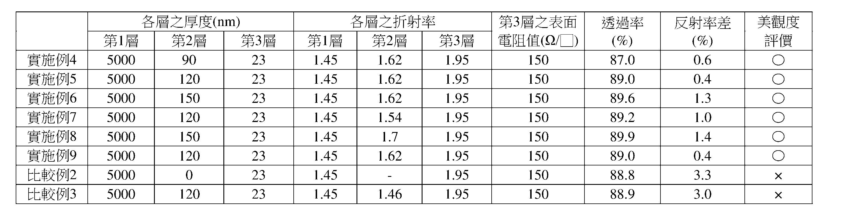
TS,於MIBK(甲基異丁基酮)中藉由超音波製作出溶液。其次,將偏二氟乙烯與三氟乙烯及三氟氯乙烯之共聚物之溶液藉由棒式塗佈機塗佈於聚對苯二甲酸乙二酯基材膜上。其次,將聚對苯二甲酸乙二酯基材膜及未乾燥之塗層以110℃、5分鐘之條件加以乾燥,而製作出塗層。表2所示之塗層15之厚度係乾燥後之厚度。 折射率調整層211如下表2所示,有折射率為1.54、1.62、1.7之情形。製造方法因折射率而異,故而針對每種折射率逐一進行說明。於折射率為1.54之情形時,在具有壓電性之塗層15之一面藉由三聚氰胺樹脂:醇酸樹脂:有機矽烷縮合物之重量比為2:2:1之熱硬化型樹脂(光之折射率n=1.54)而形成厚度為120 nm之折射率調整層211。 於折射率為1.62之情形時,在具有壓電性之塗層15之一面使用凹版塗佈機塗佈含有47質量份紫外線硬化性樹脂、57質量份氧化氧化鋯粒子(中值粒徑為40 nm)及PGME(Propylene Glycol Monomethyl Ether,丙二醇單甲醚)之光學調整組成物(JSR公司製造,「Opstar Z7412」,固形物成分為12質量%),並於無風狀態(未達0.1 m/s)下立即以60℃進行1分鐘加熱乾燥。其後,藉由高壓水銀燈照射累計光量為250 mJ/cm2
之紫外線實施硬化處理。藉由該方法,將厚度為90、120、或150 nm且折射率為1.62之折射率調整層211形成於具有壓電性之塗層15之上。 於折射率為1.7之情形時,製備在包含三聚氰胺樹脂、醇酸樹脂及有機矽烷縮合物之熱硬化型樹脂(以重量比計,三聚氰胺樹脂:醇酸樹脂:有機矽烷縮合物=2:2:1)中混合TiO2
(折射率=2.35)之微粒子而成之樹脂組成物。此時,以上述樹脂組成物之折射率成為1.70之方式調整TiO2
微粒子之混合量。然後,於具有壓電性之塗層15之上塗佈上述樹脂組成物,並使其硬化,而形成厚度為150 nm之折射率調整層211(折射率為1.70)。 再者,於第1基材膜14之與塗層15相反之面形成有具有抗黏連功能之硬塗層231。 各實施例如上所述,具有壓電性之塗層15之厚度成為0.5~10 μm,折射率調整層211之厚度成為80~160 nm,第2透明電極18之厚度成為20 nm以上。又,具有壓電性之塗層15之折射率成為1.40~1.50,折射率調整層211之折射率成為1.50~1.70,第2透明電極18之折射率成為1.90~2.10。第2透明電極18與折射率調整層211之反射率差為2%以下,美觀度較佳。 再者,視需要對第2透明電極18進行蝕刻使其成為所期望之電極等。獲得上述折射率時,折射率調整層211之折射率係使用藉由蝕刻將第2透明電極18去掉後之部分。因此,藉由自各折射率求出空氣與第2透明電極18、空氣與折射率調整層211之反射率,而求出反射率差。 [比較例2~3] 作為與實施例4~9相對之比較例,實施了無折射率調整層211之情形(比較例3)及折射率調整層211之折射率小於1.5之情形(比較例4)。於無折射率調整層211之情形時,反射率差係第2透明電極18與具有壓電性之塗層15之差。反射率差大於2%,美觀度變差。 再者,折射率為1.46之情形時(比較例4)之折射率調整層211係以如下方式製作而成:將矽溶膠(COLCOAT(股)製造,COLCOATP)以固形物成分濃度成為2%之方式藉由乙醇加以稀釋,藉由二氧化矽塗佈法將其塗佈於具有壓電性之塗層15之一面之上,其後以150℃進行2分鐘乾燥,使其硬化,形成厚度為120 nm之層(SiO2
膜,光之折射率為1.46),將其作為折射率調整層211。於比較例中,其他構成之製造方法與實施例相同。 [表2]
根據以上內容,因為於具有壓電性之塗層15之上具備第2透明電極18,故而有藉由第2透明電極18而呈現黃色或茶色從而有損美觀度之情形。可知:藉由如本發明般設置折射率調整層211,並將第2透明電極18、折射率調整層211、具有壓電性之塗層15之厚度及折射率以處於上述值之範圍內之方式加以調節,可如表2所示般縮小反射率差,而無損美觀度。可知:即便將於壓電膜16積層有折射率調整層211及第2透明電極18之構成配置於顯示器之前表面,亦不易損害顯示器之美觀度。 此外,本發明能以於不脫離其主旨之範圍內基於業者之知識施加過各種改良、修正、變更而成之態樣加以實施。 [產業上之可利用性] 本發明之觸碰感測器可配置於顯示器之前表面,與顯示器作為一體而利用。The touch sensor of the present invention will be described using figures. Regarding the configuration described in one embodiment, there are cases where the same configuration exists in other embodiments, the description of the configuration is omitted, and the same symbols are attached to the drawings. [Embodiment 1] The touch sensor 10 of the present invention shown in Figs. 1 and 2 is arranged on the display surface of the display. The touch sensor 10 of the present invention includes a piezoelectric sensor 11 and an electrostatic capacitance sensor 12. The piezoelectric sensor 11 detects the pressing force in a piezoelectric manner. The electrostatic capacitance sensor 12 detects the pressed position (X coordinate and Y coordinate) by means of electrostatic capacitance. The piezoelectric sensor 11 and the electrostatic capacitance sensor 12 are connected by a transparent filling layer 13. [Piezoelectric sensor] The piezoelectric sensor 11 includes: a piezoelectric film 16 which is a first laminate composed of a first substrate film 14 and a piezoelectric coating 15; and a first transparent electrode 17 , Which is formed on one side of the piezoelectric film 16; and the second transparent electrode 18, which is formed on the other side of the piezoelectric film 13. If the touch sensor 10 is pressed, the piezoelectric coating 15 is polarized, and the potential change at this time is detected by the transparent electrodes 17, 18, so that the pressing force can be detected. [Electrostatic capacitance sensor] The electrostatic capacitance sensor 12 is arranged on one side of the piezoelectric sensor 13. The electrostatic capacitance sensor 12 includes: a second laminated body 21 in which a third transparent electrode 20 is formed on one surface of the second base film 19; and a third laminated body 24 in which a third transparent electrode 20 is formed on one surface of the third base film 22 The fourth transparent electrode 23; and the transparent filling layer 25, which adheres the second layered body 21 and the third layered body 24. The transparent electrodes 20 and 24 are insulated from each other. When a finger or pen touches or approaches the touch sensor 10, the electrostatic capacitance at that position changes, and the potential of the transparent electrodes 20 and 24 at that position changes. The electrostatic capacitance sensor 12 can detect the change in the potential Touch the location. [Substrate film] The first, second, and third substrate films 14, 19, and 22 include, for example, polyethylene terephthalate, cycloolefin polymer, polyethylene naphthalate, polyolefin, and polyolefin. Cyclic olefin, polycarbonate, polyether agglomerate, polyarylate, polyimide, polyamide, polystyrene, polynorbornene and other polymer films. Each base film 14, 19, 22 is preferably a polyethylene terephthalate film (PET film) excellent in transparency, heat resistance, and mechanical properties, but it is not limited to this. In addition, films of different materials may be laminated to form one base film. The thickness of each base film 14, 19, 22 is preferably 10 μm or more and 150 μm or less, but it is not limited to this. Among them, if the thickness of the base films 14, 19, 22 is less than 10 μm, it may be difficult to handle. Moreover, if the thickness of the base films 14, 19, 22 exceeds 150 μm, it may be difficult to wind the piezoelectric film 16, the second laminate 21, and the third laminate 24 into a roll. [Coating with Piezoelectricity] The coating 15 with piezoelectricity is coated on any surface of the first substrate film 14 in the form of a thin film. The piezoelectric coating 15 is not particularly limited as long as the film after coating has piezoelectricity. The coating 15 having piezoelectricity is preferably one that exhibits piezoelectricity even if it is not subjected to polarization (polarization treatment), but it may also exhibit piezoelectricity after polarization. As polarization, the following two methods are known: the non-contact type, which uses corona discharge treatment to separate the electrodes; and the contact type, which uses two metal plates to sandwich the film and apply a voltage to perform the polarization. The piezoelectric coating 15 is obtained, for example, by dissolving the material of the coating 15 in a solvent to form a solution, and applying a known coating device such as a bar coater or a gravure coater to the first The base film 14 is coated thinly and uniformly, and then dried. [Material with piezoelectricity coating layer] As the material for the piezoelectricity coating layer 15, for example, a material containing fluororesin can be preferably used. If a material containing a fluororesin is specifically exemplified, it can be selected from polyvinylidene fluoride as a polymer containing vinylidene fluoride, a copolymer of vinylidene fluoride-trifluoroethylene, and vinylidene fluoride-trifluoroethylene Ethylene-chlorotrifluoroethylene copolymer, hexafluoropropylene-vinylidene fluoride copolymer, perfluorovinyl ether-vinylidene fluoride copolymer, tetrafluoroethylene-vinylidene fluoride copolymer, hexafluoro ring Propylene oxide-vinylidene fluoride copolymer, hexafluoropropylene oxide-tetrafluoroethylene-vinylidene fluoride copolymer, hexafluoropropylene-tetrafluoroethylene-vinylidene fluoride copolymer. Furthermore, these polymers may be used alone or in a mixture. More preferably, it is a copolymer of vinylidene fluoride-trifluoroethylene-chlorotrifluoroethylene, a copolymer of vinylidene fluoride-trifluoroethylene, and a polymer of vinylidene fluoride. When the vinylidene fluoride-trifluoroethylene copolymer is used as the material of the coating 15, when the molar ratio of vinylidene fluoride to trifluoroethylene is 100 as a whole, it is suitable (50~85) : (50~15). Also, when a copolymer of vinylidene fluoride-trifluoroethylene-chlorotrifluoroethylene is used as the material of the coating 15, the molar ratio of vinylidene fluoride to trifluoroethylene and chlorotrifluoroethylene is compared to the whole When it is counted as 100, it is appropriate to be (63 to 65): (27 to 29): (10 to 6). [The thickness of the coating layer with piezoelectricity] The thickness of the coating layer 15 with piezoelectricity after drying is not limited. Considering the following optical characteristics, it is preferably 0.5 μm or more and 20 μm or less, and more preferably 0.5 ~10 μm, more preferably 0.5-5 μm. If the thickness of the piezoelectric coating 15 after drying is less than 0.5 μm, the formed film may be imperfect. If the dried thickness of the piezoelectric coating 15 exceeds 20 μm, the optical properties (haze and total light transmittance) may become inappropriate. [Optical characteristics of piezoelectric film] The image of the display must be clearly visible, so the haze value of the piezoelectric film 16 is preferably less than 5%, and the total light transmittance is preferably more than 90%. When the haze value of the piezoelectric film 16 is 5% or more, or when the total light transmittance is less than 85%, the image of the display may become unclear. [Transparent electrode] The first and second transparent electrodes 17, 18 are electrodes for detecting pressing force, and the third and fourth transparent electrodes 20, 23 are electrodes for detecting pressing position. The first transparent electrode 17 covers the entire one surface of the piezoelectric film 16, and the second transparent electrode 18 covers the entire other surface of the piezoelectric film 16. When the touch sensor 10 is pressed, the piezoelectric coating 15 is polarized. At this time, the first and second transparent electrodes 17 and 18 detect the potential change of the piezoelectric coating 15. For example, the second transparent electrode 18 is set to a reference potential (ground potential), and the potential change is detected by the first transparent electrode 17. As shown in FIGS. 1 and 2, a third transparent electrode 20 and a fourth transparent electrode 23 are arranged on one surface side of the piezoelectric sensor 11. The transparent electrodes 20 and 23 are part of the electrostatic capacitance sensor 12. As shown in FIG. 1, the third transparent electrode 20 and the fourth transparent electrode 23 are insulated by providing a second base film 19 and a transparent filling layer 25 between them. Furthermore, as shown in FIG. 2, the third and fourth transparent electrodes 20 and 23 are formed in a strip shape, and the electrodes 20 and 23 face each other in orthogonal directions. For example, it is assumed that the third transparent electrode 20 is an electrode for detecting the X coordinate of the pressing position, and the fourth transparent electrode 23 is an electrode for detecting the Y coordinate. By pressing or touching the surface of the sensor 10 with a finger or a pen, the potential changes of the third and fourth transparent electrodes 20 and 23 at that position are used to detect the X and Y coordinates by using the potential changes. Furthermore, the electrostatic capacitance sensor 12 of FIG. 1 has a third transparent electrode 20 on an area layer of the second substrate film 19, and a fourth transparent electrode 23 on an area layer of the third substrate film 22, but not Limited to this structure. For example, it is also possible to layer transparent electrodes 20, 23 on one surface or another area of the base film 19, 22 like the electrostatic capacitance sensors 27, 28, 29 of Figure 3(a), (b), (c), And the laminated bodies 21 and 24 are bonded by the transparent filling layer 25. In addition, the second layered body 21 is arranged above the third layered body 24, but it may be arranged upside down. Examples of the transparent electrodes 17, 18, 20, and 23 include indium-based composite oxides. Among them, representative ones include indium tin composite oxide (ITO: Indium Tin Oxide) and indium-zinc composite oxide. Examples include indium oxide (In2O3) doped with tetravalent metal ions or divalent metal ions. The indium-based composite oxide has a transmittance of up to 80% in the visible light region (380~780 nm), and the surface resistance per unit area is low (30~1000 Ω/□ (ohms per square, ohms per square)). feature. The thickness of the indium-based composite oxide is preferably 35 nm or less. The reason is that if the thickness becomes too thick, the transmittance of the visible light region, etc., deteriorate. In addition, the surface resistance of the indium-based composite oxide is preferably 300 Ω/□ or less, and more preferably 150 Ω/□ or less. The reason is that if the surface resistance value increases, it cannot function as an electrode. A transparent electrode with a small surface resistance can be obtained, for example, by the following method: after forming an amorphous layer of indium-based composite oxide on a substrate film by sputtering or vacuum evaporation, the temperature is carried out at 80-200°C The heat treatment turns the amorphous layer into a crystalline layer. The transparent electrodes 17, 18, 20, and 23 are not limited to the above-mentioned materials, and transparent conductive oxides such as tin zinc oxide, zinc oxide, and fluorine-doped tin oxide, and conductive polymers such as polyethylenedioxythiophene can be used. When the piezoelectric coating 15 is polarized, it can be polarized after forming the first and second transparent electrodes 17, 18, or before forming the first and second transparent electrodes 17, 18 Polarize the coating. When the first and second transparent electrodes 17 and 18 are formed by sputtering, either polarization or sputtering may be the first. [Interlayer] It can also be between the first base film 14 and the piezoelectric coating 15, the first, second, and third base films 14, 19, 22, and the first, third, and fourth transparent electrodes 17 Between 20 and 23, a thin layer of several nanometers to several tens of nanometers, such as an ancher coat layer, an index matching layer (optical adjustment layer), etc., is provided. The primer layer is used to improve the adhesion between the layers, and the refractive index adjustment layer is used to adjust the reflectivity. Furthermore, an anti-adhesion layer may be provided between each base film 14, 19, 22 and the transparent electrodes 17, 20, 23. The anti-adhesion layer has the effect of preventing the accumulation of film from crimping (adhesion). [Transparent Filling Layer] The transparent filling layers 13, 25 do not form an air layer and fill the space between the layers. The surfaces of the first and fourth transparent electrodes 17 and 23 are covered with transparent filling layers 13 and 25. The purpose is to use the reflection generated on the surface of the first and fourth transparent electrodes 17 and 23 and the scattering generated by the fine unevenness to prevent the reduction of total light transmittance and haze. The transparent filling layers 13 and 25 use an adhesive or resin containing an optically transparent adhesive material or an optically transparent adhesive material. Optically transparent adhesive material or optically transparent adhesive material in sheet form can be laminated to form transparent filling layer 13, 25, or liquid optically transparent adhesive material or optically transparent adhesive material can be coated, and irradiated with ultraviolet rays to harden The transparent filling layers 13, 25 are formed. [Display] A touch sensor 10 is arranged on the front surface of the display. The display can be a flat-panel display such as a liquid crystal display or an organic EL (Electroluminescence) display. The electrostatic capacitance sensor 12 for detecting the pressing position is arranged above the piezoelectric sensor 11 (touching side). The reason is that the first and second transparent electrodes 17, 18 are formed so as to cover the piezoelectric film 16. If the piezoelectric sensor 11 is arranged above the capacitance sensor 12, the third and fourth transparent electrodes The transparent electrodes 20 and 23 cannot detect changes in electrostatic capacitance. The touch sensor 10 and the display are connected by a transparent filling layer. The transparent filling layer can use the above-mentioned optically transparent adhesive material or optically transparent adhesive material. As described above, in the present invention, the piezoelectric coating layer 15 is formed on the first base film 14 so that the thickness of the piezoelectric material can be made thinner than before. Because the piezoelectric coating 15 is thin, it is not easy to deteriorate the total light transmittance and haze. Therefore, the touch sensor 10 with good optical characteristics can be realized. [Embodiment 2] In the touch sensor 10 of FIG. 1, the direction of the piezoelectric film 16 is arbitrary. It is also possible to arrange the coating 15 with piezoelectricity on the upper side of the first base film 14 like the touch sensor 30 in FIG. 4. The touch sensor 30 of FIG. 4 has changed the direction of the piezoelectric film 16 relative to the touch sensor 10 of FIG. 1, but the direction of the piezoelectric sensor 11 can also be changed. The second transparent electrode 18 is next to the transparent filling layer 13 and arranged in the order of the second transparent electrode 18, the piezoelectric sensor 11, and the first transparent electrode 17 from top to bottom. [Embodiment 3] Like the piezoelectric sensor 41 of the touch sensor 40 in FIG. 5(a), the second transparent electrode 18 may not be directly formed on the piezoelectric film 16. The fourth laminate 43 in which the second transparent electrode 18 is laminated on the fourth base film 42 is prepared, and the piezoelectric film 16 and the fourth laminate are bonded via the transparent filling layer 44. The fourth base film 42 may be composed of the same material as the first base film 14 and the like. In addition, the transparent filling layer 44 may be composed of the same material as other transparent filling layers 13 and the like. The direction of the fourth laminate 43 is not limited. The piezoelectric sensor 41 of the touch sensor 40 in FIG. 5( a) is the second transparent electrode 18 attached to the transparent filling layer 44. The fourth base film 42 can also be attached to the transparent filling layer 44 like the piezoelectric sensor 46 of the touch sensor 45 in FIG. 5(b). Furthermore, this embodiment can be applied to the touch sensor 30 of FIG. 4. In the touch sensor 30, instead of directly forming the second transparent electrode 18 on the first base film 14, a fourth laminate 43 is prepared, and the first base film and the fourth laminate 43 are formed by The transparent filling layer 44 is then attached. The direction of the fourth layered body 43 is not limited, and it does not matter which of the second transparent electrode 18 and the fourth base film 42 is attached to the transparent filling layer 44. [Embodiment 4] Like the piezoelectric sensor 51 of the touch sensor 50 in FIG. 6(a), the first transparent electrode 17 may not be directly formed on the piezoelectric film 16. The fifth laminate 53 in which the first transparent electrode 17 is laminated on the fifth base film 52 is prepared, and the piezoelectric film 16 and the fifth laminate 53 are bonded by the transparent filling layer 54. The fifth base film 52 may be composed of the same material as the first base film 14 and the like. In addition, the transparent filling layer 54 can be made of the same material as other transparent filling layers 13 and the like. The direction of the fifth layered body 53 is not limited. The piezoelectric sensor 51 of the touch sensor 50 of FIG. 6(a) is the fifth base film 52 and then the transparent filling layer 54. The first transparent electrode 17 can also be attached to the transparent filling layer 54 as in the piezoelectric sensor 56 of the touch sensor 55 in FIG. 6(b). Furthermore, this embodiment can be applied to the touch sensor 30 of FIG. 4. In the touch sensor 30, instead of directly forming the first transparent electrode 17 on the piezoelectric coating 15, a fifth laminate 53 is prepared, and the piezoelectric coating 15 and the fifth The laminated body 53 is adhered by the transparent filling layer 54. The direction of the fifth layered body 53 is not limited, and it does not matter which one of the first transparent electrode 17 and the fifth base film 52 is attached to the transparent filling layer 54. [Embodiment 5] The piezoelectric film 16, the fourth laminate 43, and the fifth laminate 53 of the piezoelectric sensor 61 of the touch sensor 60 of FIG. constitute. The piezoelectric sensor 61 is a combination of the piezoelectric sensor 41 of FIG. 5 and the piezoelectric sensor 51 of FIG. 6. In the piezoelectric sensor 61, the directions of the piezoelectric film 16, the fourth laminate 43, and the fifth laminate 53 are arbitrary. The positions of the first base film 14 and the piezoelectric coating layer 15, the positions of the second transparent electrode 18 and the fourth base film 42, and the positions of the first transparent electrode 17 and the fifth base film 52 are interchangeable . Therefore, there are 8 types of piezoelectric sensor 61 configurations. [Embodiment 6] The capacitance sensor 71 of the touch sensor 70 in FIG. 8 is formed with a third transparent electrode 20 on one side of the sixth base film 72 and formed on the other side of the sixth base film 72 There is a fourth transparent electrode 23. For the sixth base film 72, the same ones as those of the first base film 14 and the like can be used. In FIG. 8, the fourth transparent electrode 23 is attached to the transparent filling layer 13, but the third transparent electrode 20 may be attached to the transparent filling layer 13. Compared with the electrostatic capacitance sensor 12 of FIG. 1 in the electrostatic capacitance sensor 71 of FIG. 8, the number of substrate films and the number of transparent filling layers are reduced. Therefore, the thickness of the touch sensor 70 can be reduced. The electrostatic capacitance sensor 12 used in the touch sensors 10, 30, 40, 45, 50, 55, and 60 described in the first to sixth embodiments can be changed to an electrostatic capacitance sensor 71. [Embodiment 7] The electrostatic capacitance sensor 81 of the touch sensor 80 of Fig. 9(a) has a 3'transparent electrode 82 and a 4'transparent electrode 83 formed on one surface side of the sixth base film 72 . The third' transparent electrode 82 and the fourth' transparent electrode 83 are formed of the same material as the third transparent electrode 20 and the fourth transparent electrode 23. As shown in Figure 9(b), the 3'transparent electrode 82 and the 4'transparent electrode 83 are arranged with a plurality of rectangular portions 85 and 86 respectively, and the rectangular portions 85 and 86 are mutually arranged in the X direction or the Y direction. The shaped parts 87 and 88 are connected. Therefore, the 3'th transparent electrode 82 and the 4th' transparent electrode 83 face mutually orthogonal directions. The rectangular portions 85 and 86 are in the shape of a rhombus, a square, a hexagon, or the like. The 3'transparent electrode 82 and the 4'transparent electrode 83 intersect with each other via an insulator 84 in order to avoid a short circuit. In FIG. 9, the 3′ transparent electrode 82 crosses the 4′ transparent electrode 83, but the 4′ transparent electrode 83 may cross the 3′ transparent electrode 82. The direction of the electrostatic capacitance sensor 81 is not limited, and the transparent electrodes 82 and 83 may be connected to the transparent filling layer 13 as well. The electrostatic capacitance sensor 12 used in the touch sensors 10, 30, 40, 45, 50, 55, and 60 described in the first to sixth embodiments can be changed to an electrostatic capacitance sensor 81. [Embodiment 8] The electrostatic capacitance sensor is not limited to a configuration in which two transparent electrodes 20 and 23 detect changes in electrostatic capacitance. The electrostatic capacitance sensor 91 of the touch sensor 90 of FIG. A lead wire 93 is connected to the rectangular transparent electrode 92. The rectangular transparent electrode 92 and the lead wire 93 are formed of the same material as the third transparent electrode 20 and the fourth transparent electrode 23. The electrostatic capacitance sensor 12 used in the touch sensors 10, 30, 40, 45, 50, 55, and 60 described in the first to sixth embodiments can be changed to an electrostatic capacitance sensor 91. [Embodiment 9] This case is not limited to the form in which the electrostatic capacitance sensor and the piezoelectric sensor are completely separated. For example, compared with the touch sensor 10 of FIG. 1, the touch sensor 100 of FIG. 11(a) omits the first transparent electrode 17. The fourth transparent electrode 23 arranged on one side of the piezoelectric film 16 is an electrode that detects the coordinates of the touch position by means of electrostatic capacitance, and is an electrode that detects the potential of the piezoelectric coating 15 when it is polarized. The fourth transparent electrode 23 also has the function of the first transparent electrode 17 of the above-mentioned embodiment. In the touch sensor 100, the piezoelectric sensor 101 and the electrostatic capacitance sensor 12 can be driven. When the piezoelectric sensor 101 operates, the fourth transparent electrode 23 and the second transparent electrode 18 are used. When the capacitance sensor 12 is operating, the third transparent electrode 20 and the fourth transparent electrode 23 are used. When the piezoelectric sensor 101 and the electrostatic capacitance sensor 12 are driven, the method of detecting the potential by the electrodes 18, 20, and 23 is the same as that of the above-mentioned embodiment. If the fourth transparent electrode 23 is used for the piezoelectric sensor 101 and the electrostatic capacitance sensor 12, the driving method of the piezoelectric sensor 101 and the electrostatic capacitance sensor 12 is not limited. It can also be the piezo-inductance of the touch sensor 102 shown in Figure 11(b). Compared with Figure 11(a), the piezoelectric coating 15 and the first substrate film 14 are replaced in positions.测器103. Compared with the touch sensor 10 in FIG. 1, the touch sensors 100 and 102 omit the first transparent electrode 17, so that the touch sensors 100 and 102 can be thinned. [Embodiment 10] In addition, it may be a structure in which the second transparent electrode 18 is not directly formed on the piezoelectric film 16 as in the piezoelectric sensor 111 of the touch sensor 110 in FIG. 12(a). As with the piezoelectric sensors 41 and 46 in FIG. 5, the piezoelectric sensor 111 is prepared on any area of the fourth substrate film 42 with the fourth laminate 43 with the second transparent electrode 18 layered, and by The transparent filling layer 44 adheres the fourth layered body 43 and the piezoelectric film 16. As with the touch sensors 100 and 102 in FIG. 11, the touch sensor 110 is the fourth transparent electrode 23 used for the capacitance sensor 12 and the piezoelectric sensor 111. If the fourth transparent electrode 24 is used for the electrostatic capacitance sensor 12 and the piezoelectric sensor 111, the driving method of the electrostatic capacitance sensor 12 and the piezoelectric sensor 111 is not limited. When the capacitance sensor 12 is driven, the third transparent electrode 20 and the fourth transparent electrode 23 are used. When the piezoelectric sensor 111 is driven, the second transparent electrode 18 and the fourth transparent electrode 23 are used. Like the piezoelectric sensor 113 of the touch sensor 112 in FIG. 12(b), the direction of the fourth laminate 43 relative to the piezoelectric sensor 111 may be changed. The fourth base film 43 is attached to the transparent filling layer 44. Furthermore, the piezoelectric sensors 111 and 113 of FIGS. 12(a) and (b) can also change the direction of the piezoelectric film 16. In FIG. 12, the piezoelectric coating 15 is located on the first substrate film 14, but the first substrate film 14 may also be located on the piezoelectric coating 15. [Embodiment 11] The fourth transparent electrode 23 may be directly formed on the piezoelectric film 16 like the touch sensor 120 of FIG. 13(a). A fourth transparent electrode 23 is layered on one area of the piezoelectric film 16, and a second transparent electrode 18 is layered on the other area of the piezoelectric film 16. The third transparent electrode 20 to the fourth transparent electrode 23 becomes 121, and the fourth transparent electrode 23 to the second transparent electrode 18 becomes the piezoelectric sensor 122. The touch sensor 120 is the same as the touch sensors 100, 102, 110, and 112 in FIGS. 11 and 12, and the fourth transparent electrode 23 is used for the capacitance sensor 121 and the piezoelectric sensor 122. It is also possible to change the direction of the piezoelectric film 16 compared to the piezoelectric sensor 122 as in the piezoelectric sensor 124 of the touch sensor 123 in FIG. 13(b). In the piezoelectric sensor 124, a fourth transparent electrode 23 is laminated on a coating layer 15 having piezoelectricity, and a second transparent electrode 18 is laminated on the first base film 14. [Embodiment 12] Like the piezoelectric sensor 131 of the touch sensor 130 in FIG. 14(a), the second transparent electrode 18 may not be directly formed on the piezoelectric film 16. Similar to the piezoelectric sensors 41 and 46 in FIG. 5, the piezoelectric sensor 131 is prepared on any area of the fourth substrate film 42 with the fourth laminate 43 with the second transparent electrode 18 layered, and by The transparent filling layer 44 adheres the fourth layered body 43 and the piezoelectric film 16. Moreover, the direction of the piezoelectric film 16 can also be changed like the piezoelectric sensor 133 of the touch sensor 132 in FIG. 14(b). A fourth transparent electrode 23 is laminated on the coating 15 having piezoelectricity. Furthermore, in the piezoelectric sensors 131 and 133 of FIG. 14, the direction of the fourth laminate 43 can also be changed. The fourth base film 42 of the fourth laminate 43 is bonded to the transparent adhesive layer 44. [Embodiment 13] In Embodiments 11 and 12, the capacitance sensor 71 of FIG. 8 can also be used. Like the touch sensor 140 in Fig. 15(a), a capacitance sensor 71 with a third transparent electrode 20 on one area of the sixth substrate film 72 and a fourth transparent electrode 23 on the other area is used . The piezoelectric sensor 141 is attached to the second transparent electrode 18 on another area of the piezoelectric film 16, and one side is attached to the transparent filling layer 25. The transparent filling layer 25 is next to the fourth transparent electrode 23, and the piezoelectric sensor 141 is formed from the fourth transparent electrode 23 to the second transparent electrode 18. In this embodiment, similarly, if the fourth transparent electrode 23 is used for the electrostatic capacitance sensor 71 and the piezoelectric sensor 141, the driving method of the electrostatic capacitance sensor 71 and the piezoelectric sensor 141 is not affected. limited. In addition, as in the piezoelectric sensor 143 of the touch sensor 142 in FIG. 15(b), the second transparent electrode 18 may be laminated on the first substrate film 14, and a coating 15 having piezoelectricity may be applied. Then on the transparent filling layer 25. Furthermore, the second transparent electrode 18 may not be directly formed on the piezoelectric film 16, and the second transparent electrode 18 may be laminated on the fourth base film 42 like the touch sensors 130 and 132 in FIG. In the fourth laminate 43, the piezoelectric film 16 and the fourth laminate 43 are bonded by a transparent filling layer 44. The surface of the transparent filling layer 44 next to the fourth laminate 43 is not limited. [Embodiment 14] Like the touch sensor 150 of Fig. 16(a), the electrostatic capacitance sensor 81 of Fig. 9 can also be used. A second transparent electrode 18 is laminated on the piezoelectric coating 15 of the piezoelectric film 16, and the first base film 14 and the sixth base film 72 are bonded by the transparent filling layer 13. The piezoelectric sensor 151 extends from the second transparent electrode 18 to the fourth ′ transparent electrode 83 of the electrostatic capacitance sensor 81. If the 4'th transparent electrode 83 is used for the electrostatic capacitance sensor 81 and the piezoelectric sensor 151, the driving method of the electrostatic capacitance sensor 81 and the piezoelectric sensor 151 is not limited. In addition, as in the piezoelectric sensor 153 of the touch sensor 152 in FIG. 16(b), the second transparent electrode 18 may be laminated on the first substrate film 14 and the coating 15 having piezoelectricity may be applied. Then on the transparent filling layer 13. Furthermore, the second transparent electrode 18 may not be directly formed on the piezoelectric film 16, and the second transparent electrode 18 may be laminated on the fourth base film 42 like the touch sensors 130 and 132 in FIG. In the fourth laminate 43, the piezoelectric film 16 and the fourth laminate 43 are bonded by a transparent filling layer 44. The surface of the transparent filling layer 44 next to the fourth laminate 43 is not limited. [Embodiment 15] An electrostatic capacitance sensor 161 like the touch sensor 160 of FIG. 17(a) can also be used. The electrostatic capacitance sensor 161 is formed with transparent electrodes 82 and 83 in two directions of the electrostatic capacitance sensor 81 of FIG. 9 on one surface side of the piezoelectric film 16. Furthermore, for the convenience of description, the capacitance sensor 161 is arranged above the piezoelectric film 16, but the capacitance sensor 161 may also be arranged above the 4′ transparent electrode 83. The piezoelectric sensor 162 of the touch sensor 160 is formed with a 4'transparent electrode 83 on one side of the piezoelectric film 16 and a second transparent electrode 18 on the other side. As with the touch sensors 150 and 152 of FIG. 16, if the 4'th transparent electrode 83 is used for the electrostatic capacitance sensor 81 and the piezoelectric sensor 151, the electrostatic capacitance sensor 81 and the piezoelectric sensor The driving method of the device 151 is not limited. In addition, like the piezoelectric sensor 165 of the touch sensor 164 in FIG. 17(b), the second transparent electrode 18 may be laminated on the first substrate film 14 and the coating 15 having piezoelectricity may be applied. Then on the transparent filling layer 13. Furthermore, the second transparent electrode 18 may not be directly formed on the piezoelectric film 16, but as in the above-mentioned embodiment, a fourth laminate 43 in which the second transparent electrode 18 is laminated on the fourth base film 42 may be prepared, and The piezoelectric film 16 and the fourth layered body 43 are bonded by the transparent filling layer 44. The surface of the transparent filling layer 44 next to the fourth laminate 43 is not limited. [Embodiment 16] The transparent electrodes located on one side and the other side of the piezoelectric film 16 can also be used for both the electrostatic capacitance sensor and the piezoelectric sensor. For example, like the touch sensor 170 in FIG. 18, the third transparent electrode 20 may be layered on one area of the piezoelectric film 16, and the fourth transparent electrode 23 may be layered on the other area of the piezoelectric film 16. The third transparent electrode 20 and the fourth transparent electrode 23 are electrodes for detecting the coordinates of the touch position by means of electrostatic capacitance, and are electrodes for detecting the potential when the piezoelectric coating 15 is polarized. If the third transparent electrode 20 and the fourth transparent electrode 23 are used for the electrostatic capacitance sensor 171 and the piezoelectric sensor 172, the driving method of the electrostatic capacitance sensor 170 and the piezoelectric sensor 172 is not limited. When the electrostatic capacitance sensor 171 is driven, the transparent electrodes 20 and 23 detect the change of the electrostatic capacitance. When the piezoelectric sensor 172 is driven, one transparent electrode 20, 23 becomes the ground potential, and the other electrode 23, 20 detects the potential change caused by the polarization of the coating layer 15. The up and down direction of the piezoelectric sensor 16 is arbitrary. The fourth transparent electrode 23 may be laminated on the first base film 14 and the third transparent electrode 20 may be laminated on the coating layer 15 having piezoelectricity. It is not limited to directly forming the transparent electrodes 20 and 23 on the piezoelectric film 16. For example, as in the touch sensor 190 of FIG. 19(a), a third layered body 24 in which a fourth transparent electrode 23 is laminated on a third base film 22 may be prepared, and the transparent filling layer 44 may be used to separate the third layered body 24 The three-layered body 24 is attached to the piezoelectric film 16. In the same manner as described above, the electrostatic capacitance sensor 191 and the piezoelectric sensor 192 alternately use the same transparent electrodes 20 and 23. In addition, the touch sensor 193 of FIG. 19(b) prepares the second laminate 21 in which the third transparent electrode 20 is laminated on the second base film 19, and the second laminate 21 is attached to the piezoelectric film 16 . Similar to the above, the electrostatic capacitance sensor 194 and the piezoelectric sensor 195 alternately use the same transparent electrodes 20 and 23. Furthermore, the touch sensor 196 of FIG. 19(c) prepares the above-mentioned second laminated body 21 and the third laminated body 24, and attaches them to the piezoelectric film 16. Similar to the above, the electrostatic capacitance sensor 197 and the piezoelectric sensor 198 alternately use the same transparent electrodes 20 and 23. In FIG. 19, the direction of the piezoelectric film 16 is not limited, and the position of the first base film 14 and the piezoelectric coating layer 15 may be exchanged, and the first base film 14 is next to the transparent filling layer 44 . In addition, the direction of the second laminate 21 is not limited, and the third transparent electrode 20 may be attached to the transparent filling layer 25. Furthermore, the direction of the third layered body 24 is not limited, and the third layered body 22 may be attached to the transparent filling layer 44. At least one of the ancher coat layer, the index matching layer (optical adjustment layer), and the anti-blocking layer described in the first embodiment may be formed on the piezoelectric film 16 and the first layer. Between 3 and 4th transparent electrodes 20 and 23. [Embodiment 17] In each embodiment, a transparent electrode may be arranged between the touch sensor and the display. For example, like the touch sensor 200 in FIG. 20, a laminate in which the seventh transparent electrode 201 is laminated on one surface of the seventh base film 202 is prepared, and the laminate is adhered by a transparent filling layer 203. The seventh transparent electrode 201 functions as a shield. [Embodiment 18] In the above embodiment, the refractive index adjustment layer was described, but the refractive index adjustment layer may be arranged between the piezoelectric film 16 and the second transparent electrode 18 like the touch sensor 210 of FIG. 21层210。 Layer 210. The touch sensor 210 of FIG. 21 has the same structure as the touch sensor 10 of FIG. 1 except that a refractive index adjustment layer 210 is added to the touch sensor 10 of FIG. 1. In addition, the refractive index adjustment layer 210 may be disposed between the piezoelectric film 16 and the first transparent electrode 17. As an example, the thickness of the piezoelectric coating layer 15 can be 0.5-10 μm, as an example the thickness of the refractive index adjustment layer 210 can be 80-160 nm, and as the thickness of the second transparent electrode 18 it can be 20 nm or more. As an example. In addition, as an example, the refractive index of the coating layer 15 having piezoelectricity is 1.40 to 1.50, as an example the refractive index of the refractive index adjustment layer 210 is 1.50 to 1.70, and as an example the refractive index of the second transparent electrode 18 1.90~2.10 is an example. In addition, the thickness of the first base film 14 is set to 2 to 100 μm, and the refractive index is set to 1.50 to 1.70. By setting the above thickness and refractive index, the reflectance difference between the second transparent electrode 18 and the refractive index adjustment layer 210 becomes 2.0% or less, and the aesthetics is improved. [Examples 1 to 3] In FIG. 12, the total light transmittance and haze of the touch sensor 10 when the thickness of the coating layer 15 is 1 μm, 5 μm, and 10 μm are measured, and the The results are shown in Table 1. Coating 15 uses P (VDF-TrFE) (copolymer of vinylidene fluoride and trifluoroethylene) with a molar ratio of 72:25. The base film 14 uses PET, and its thickness is 23 μm. The total light transmittance and haze were measured using a direct reading haze computer (HGM-ZDP manufactured by Suga Test Instruments). [Comparative Example 1] Furthermore, as a comparative example, for the touch sensor 220 shown in FIG. 22, the piezoelectric film 222 is attached to the first base film 14 through the transparent filling layer 221. Measure the total light transmittance and haze. The piezoelectric film 222 is a separate film manufactured by extrusion using PVDF (polyvinylidene fluoride), with a thickness of 80 μm. The transparent filling layer 221 uses an optically transparent adhesive, and its thickness is 22 μm. The other configurations are the same as in the case of the embodiment. [Table 1] It can be seen from Table 1 that the total light transmittance and haze of all the examples are better than those of the comparative examples. For the comparative example, it is considered that the thickness of the piezoelectric film 222 becomes too thick, and the haze particularly deteriorates due to the thickness. [Examples 4-9] Also, in order to confirm the change in appearance caused by the refractive index adjustment layer 211 of FIG. 21, a piezoelectric film was fabricated on the first substrate film 14 with a thickness of 23 μm as shown in FIG. For the flexible coating 15, the refractive index adjustment layer 211, and the second transparent electrode 18, the thickness and refractive index were measured. The results are shown in Table 2. The “first layer” is the piezoelectric coating 15, the “second layer” is the refractive index adjustment layer 211, and the “third layer” is the second transparent electrode 18. The piezoelectric film 16 is made by coating a polyethylene terephthalate substrate film with a copolymer of vinylidene fluoride, trifluoroethylene, and chlorotrifluoroethylene. The copolymer of vinylidene fluoride, trifluoroethylene and chlorotrifluoroethylene is Piezotech RT manufactured by Arkema Co., Ltd. TM TS, in MIBK (methyl isobutyl ketone) by ultrasound to make a solution. Secondly, the solution of the copolymer of vinylidene fluoride, trifluoroethylene and chlorotrifluoroethylene was coated on the polyethylene terephthalate substrate film by a bar coater. Next, the polyethylene terephthalate base film and the undried coating are dried at 110°C for 5 minutes to produce the coating. The thickness of the coating 15 shown in Table 2 is the thickness after drying. As shown in Table 2 below, the refractive index adjustment layer 211 may have a refractive index of 1.54, 1.62, or 1.7. The manufacturing method differs depending on the refractive index, so each refractive index will be explained one by one. When the refractive index is 1.54, the melamine resin: alkyd resin: organosilane condensate with a weight ratio of 2:2:1 is used on one side of the coating 15 with piezoelectricity. Refractive index n=1.54) to form a refractive index adjustment layer 211 with a thickness of 120 nm. When the refractive index is 1.62, use a gravure coater to coat 47 parts by mass of ultraviolet curable resin and 57 parts by mass of zirconia particles (median particle size is 40 nm) and PGME (Propylene Glycol Monomethyl Ether, propylene glycol monomethyl ether) optical adjustment composition (made by JSR company, "Opstar Z7412", solid content of 12% by mass), and in a no-wind state (less than 0.1 m/s ) Immediately heat and dry at 60°C for 1 minute. After that, the cumulative amount of light irradiated by the high-pressure mercury lamp is 250 mJ/cm 2 The ultraviolet rays are hardened. By this method, a refractive index adjustment layer 211 with a thickness of 90, 120, or 150 nm and a refractive index of 1.62 is formed on the coating layer 15 having piezoelectricity. When the refractive index is 1.7, it is prepared in a thermosetting resin containing melamine resin, alkyd resin and organosilane condensate (by weight ratio, melamine resin: alkyd resin: organosilane condensate = 2:2: 1) Medium mixed TiO 2 (Refractive index = 2.35) A resin composition made of fine particles. At this time, adjust the TiO so that the refractive index of the above resin composition becomes 1.70 2 The mixing amount of fine particles. Then, the above-mentioned resin composition is coated on the piezoelectric coating layer 15 and cured to form a refractive index adjustment layer 211 (refractive index: 1.70) with a thickness of 150 nm. Furthermore, a hard coat layer 231 having an anti-blocking function is formed on the surface of the first base film 14 opposite to the coating layer 15. In each embodiment, as described above, the thickness of the piezoelectric coating layer 15 is 0.5-10 μm, the thickness of the refractive index adjustment layer 211 is 80-160 nm, and the thickness of the second transparent electrode 18 is 20 nm or more. In addition, the refractive index of the piezoelectric coating 15 is 1.40 to 1.50, the refractive index of the refractive index adjustment layer 211 is 1.50 to 1.70, and the refractive index of the second transparent electrode 18 is 1.90 to 2.10. The reflectance difference between the second transparent electrode 18 and the refractive index adjustment layer 211 is 2% or less, and the aesthetics is better. Furthermore, if necessary, the second transparent electrode 18 is etched to become a desired electrode or the like. When the above-mentioned refractive index is obtained, the refractive index of the refractive index adjustment layer 211 is the portion obtained by removing the second transparent electrode 18 by etching. Therefore, the reflectance difference between the air and the second transparent electrode 18, the air and the refractive index adjustment layer 211 is obtained from each refractive index, and the reflectance difference is obtained. [Comparative Examples 2 to 3] As a comparative example to Examples 4 to 9, the case where the refractive index adjustment layer 211 is not provided (Comparative Example 3) and the case where the refractive index of the refractive index adjustment layer 211 is less than 1.5 (Comparative Example 4). When there is no refractive index adjustment layer 211, the difference in reflectance is the difference between the second transparent electrode 18 and the coating 15 having piezoelectricity. The reflectance difference is greater than 2%, and the aesthetics deteriorates. Furthermore, when the refractive index is 1.46 (Comparative Example 4), the refractive index adjustment layer 211 is made as follows: Silica sol (manufactured by COLCOAT (Co., Ltd., COLCOATP)) has a solid content concentration of 2% The method is diluted by ethanol, and coated on one side of the piezoelectric coating 15 by the silicon dioxide coating method, and then dried at 150°C for 2 minutes to harden it to form a thickness of 120 nm layer (SiO 2 The refractive index of light is 1.46), which is used as the refractive index adjustment layer 211. In the comparative example, the manufacturing method of other configurations is the same as that of the embodiment. [Table 2] According to the above, since the second transparent electrode 18 is provided on the coating layer 15 having piezoelectricity, the second transparent electrode 18 may appear yellow or brown, which may impair the aesthetics. It can be seen that by providing the refractive index adjustment layer 211 as in the present invention, the thickness and refractive index of the second transparent electrode 18, the refractive index adjustment layer 211, and the piezoelectric coating 15 are within the above-mentioned range of values. The method can be adjusted to reduce the reflectivity difference as shown in Table 2 without compromising the aesthetics. It can be seen that even if the piezoelectric film 16 is laminated with the refractive index adjustment layer 211 and the second transparent electrode 18 on the front surface of the display, the aesthetics of the display is not easily impaired. In addition, the present invention can be implemented in a state in which various improvements, corrections, and changes have been made based on the knowledge of the industry within the scope not departing from the spirit of the invention. [Industrial Applicability] The touch sensor of the present invention can be arranged on the front surface of the display and used as a whole with the display.
10、30、40、45、50、55、60、70‧‧‧觸碰感測器
80、90、100、102、110、112、120、123、130、132、140、142、 150、152、160、164、170、190、193、196、200、210 11、41、46、56、61、101、103‧‧‧壓電感測器
111、113、122、124、131、133、141、143、151、153、162、165、172、192、195、198 12、27、28、29、71、81、91‧‧‧ 靜電電容感測器
121、161、171、191、194、197 13、25、44、183‧‧‧透明填充層
14、19、22、42、52、72、182‧‧‧基材膜
15‧‧‧具有壓電性之塗層
16、21、24、43、53、62、71、81‧‧‧積層體
17、18、20、23、82、83、92、181‧‧‧透明電極
84‧‧‧絕緣體
211‧‧‧折射率調整層
231‧‧‧具有抗黏連功能之硬塗層
10, 30, 40, 45, 50, 55, 60, 70‧‧‧Touch sensor
80, 90, 100, 102, 110, 112, 120, 123, 130, 132, 140, 142, 150, 152, 160, 164, 170, 190, 193, 196, 200, 210 11, 41, 46, 56 , 61, 101, 103‧‧‧piezoelectric sensor
111, 113, 122, 124, 131, 133, 141, 143, 151, 153, 162, 165, 172, 192, 195, 198 12, 27, 28, 29, 71, 81, 91‧‧‧ Electrostatic capacitance Detector
121, 161, 171, 191, 194, 197 13, 25, 44, 183‧‧‧transparent filling layer
14, 19, 22, 42, 52, 72, 182‧‧‧Base film
15‧‧‧Coating with piezoelectricity
16, 21, 24, 43, 53, 62, 71, 81‧‧‧Layered body
17, 18, 20, 23, 82, 83, 92, 181‧‧‧Transparent electrode
84‧‧‧Insulator
211‧‧‧Refractive index adjustment layer
231‧‧‧Hard coating with anti-blocking function
圖1係模式性表示本發明之觸碰感測器之構成之圖。 圖2係將圖1之觸碰感測器分解為各個構成零件而成之立體圖。 圖3(a)~(c)係模式性表示靜電電容感測器之另一構成之圖。 圖4係模式性表示本發明之實施形態2之觸碰感測器之構成之圖。 圖5(a)、(b)係模式性表示本發明之實施形態3之觸碰感測器之構成之圖。 圖6(a)、(b)係模式性表示本發明之實施形態4之觸碰感測器之構成之圖。 圖7係模式性表示本發明之實施形態5之觸碰感測器之構成之圖。 圖8係模式性表示本發明之實施形態6之觸碰感測器之構成之圖。 圖9(a)、(b)係模式性表示本發明之實施形態7之觸碰感測器之構成之圖。 圖10(a)、(b)係模式性表示本發明之實施形態8之觸碰感測器之構成之圖。 圖11(a)、(b)係模式性表示本發明之實施形態9之觸碰感測器之構成之圖。 圖12(a)、(b)係模式性表示本發明之實施形態10之觸碰感測器之構成之圖。 圖13(a)、(b)係模式性表示本發明之實施形態11之觸碰感測器之構成之圖。 圖14(a)、(b)係模式性表示本發明之實施形態12之觸碰感測器之構成之圖。 圖15(a)、(b)係模式性表示本發明之實施形態13之觸碰感測器之構成之圖。 圖16(a)、(b)係模式性表示本發明之實施形態14之觸碰感測器之構成之圖。 圖17(a)、(b)係模式性表示本發明之實施形態15之觸碰感測器之構成之圖。 圖18係模式性表示本發明之實施形態16之觸碰感測器之構成之圖。 圖19(a)~(c)係模式性表示本發明之實施形態16之觸碰感測器之另一構成之圖。 圖20係模式性表示本發明之實施形態17之觸碰感測器之構成之圖。 圖21係模式性表示本發明之實施形態18之觸碰感測器之構成之圖。 圖22係模式性表示比較例之觸碰感測器之構成之圖。 圖23係模式性表示進行了實施例4~10之構成之圖。FIG. 1 is a diagram schematically showing the structure of the touch sensor of the present invention. Fig. 2 is a perspective view of the touch sensor of Fig. 1 broken down into its constituent parts. 3(a) to (c) are diagrams schematically showing another configuration of the capacitance sensor. Fig. 4 is a diagram schematically showing the structure of the touch sensor in the second embodiment of the present invention. 5(a) and (b) are diagrams schematically showing the structure of the touch sensor in the third embodiment of the present invention. Fig. 6 (a) and (b) are diagrams schematically showing the structure of the touch sensor in the fourth embodiment of the present invention. Fig. 7 is a diagram schematically showing the structure of a touch sensor according to the fifth embodiment of the present invention. Fig. 8 is a diagram schematically showing the structure of the touch sensor in the sixth embodiment of the present invention. Figures 9(a) and (b) are diagrams schematically showing the structure of the touch sensor in the seventh embodiment of the present invention. Fig. 10 (a) and (b) are diagrams schematically showing the structure of the touch sensor in the eighth embodiment of the present invention. Fig. 11 (a) and (b) are diagrams schematically showing the structure of the touch sensor in the ninth embodiment of the present invention. Fig. 12 (a) and (b) are diagrams schematically showing the structure of the touch sensor according to the tenth embodiment of the present invention. Fig. 13 (a) and (b) are diagrams schematically showing the structure of the touch sensor according to the eleventh embodiment of the present invention. 14(a) and (b) are diagrams schematically showing the structure of the touch sensor in the twelfth embodiment of the present invention. Fig. 15 (a) and (b) are diagrams schematically showing the structure of the touch sensor in the thirteenth embodiment of the present invention. Fig. 16 (a) and (b) are diagrams schematically showing the structure of the touch sensor according to Embodiment 14 of the present invention. Fig. 17(a) and (b) are diagrams schematically showing the structure of the touch sensor according to the fifteenth embodiment of the present invention. Fig. 18 is a diagram schematically showing the structure of a touch sensor according to the sixteenth embodiment of the present invention. Figures 19(a) to (c) are diagrams schematically showing another configuration of the touch sensor according to the sixteenth embodiment of the present invention. Fig. 20 is a diagram schematically showing the structure of a touch sensor according to the seventeenth embodiment of the present invention. Fig. 21 is a diagram schematically showing the structure of a touch sensor according to the eighteenth embodiment of the present invention. Fig. 22 is a diagram schematically showing the structure of the touch sensor of the comparative example. Fig. 23 is a diagram schematically showing the configuration of Examples 4-10.