RU2477546C2 - Light-emitting diode for lateral radiation with silicone lens supported by curvilinear silicone section - Google Patents
Light-emitting diode for lateral radiation with silicone lens supported by curvilinear silicone section Download PDFInfo
- Publication number
- RU2477546C2 RU2477546C2 RU2010109737/28A RU2010109737A RU2477546C2 RU 2477546 C2 RU2477546 C2 RU 2477546C2 RU 2010109737/28 A RU2010109737/28 A RU 2010109737/28A RU 2010109737 A RU2010109737 A RU 2010109737A RU 2477546 C2 RU2477546 C2 RU 2477546C2
- Authority
- RU
- Russia
- Prior art keywords
- light
- light emitting
- emitting diode
- optical element
- silicone
- Prior art date
Links
Images


Classifications
-
- H—ELECTRICITY
- H01—ELECTRIC ELEMENTS
- H01L—SEMICONDUCTOR DEVICES NOT COVERED BY CLASS H10
- H01L33/00—Semiconductor devices with at least one potential-jump barrier or surface barrier specially adapted for light emission; Processes or apparatus specially adapted for the manufacture or treatment thereof or of parts thereof; Details thereof
- H01L33/48—Semiconductor devices with at least one potential-jump barrier or surface barrier specially adapted for light emission; Processes or apparatus specially adapted for the manufacture or treatment thereof or of parts thereof; Details thereof characterised by the semiconductor body packages
- H01L33/58—Optical field-shaping elements
-
- H—ELECTRICITY
- H01—ELECTRIC ELEMENTS
- H01L—SEMICONDUCTOR DEVICES NOT COVERED BY CLASS H10
- H01L33/00—Semiconductor devices with at least one potential-jump barrier or surface barrier specially adapted for light emission; Processes or apparatus specially adapted for the manufacture or treatment thereof or of parts thereof; Details thereof
- H01L33/44—Semiconductor devices with at least one potential-jump barrier or surface barrier specially adapted for light emission; Processes or apparatus specially adapted for the manufacture or treatment thereof or of parts thereof; Details thereof characterised by the coatings, e.g. passivation layer or anti-reflective coating
- H01L33/46—Reflective coating, e.g. dielectric Bragg reflector
-
- H—ELECTRICITY
- H01—ELECTRIC ELEMENTS
- H01L—SEMICONDUCTOR DEVICES NOT COVERED BY CLASS H10
- H01L27/00—Devices consisting of a plurality of semiconductor or other solid-state components formed in or on a common substrate
-
- H—ELECTRICITY
- H01—ELECTRIC ELEMENTS
- H01L—SEMICONDUCTOR DEVICES NOT COVERED BY CLASS H10
- H01L33/00—Semiconductor devices with at least one potential-jump barrier or surface barrier specially adapted for light emission; Processes or apparatus specially adapted for the manufacture or treatment thereof or of parts thereof; Details thereof
-
- G—PHYSICS
- G02—OPTICS
- G02F—OPTICAL DEVICES OR ARRANGEMENTS FOR THE CONTROL OF LIGHT BY MODIFICATION OF THE OPTICAL PROPERTIES OF THE MEDIA OF THE ELEMENTS INVOLVED THEREIN; NON-LINEAR OPTICS; FREQUENCY-CHANGING OF LIGHT; OPTICAL LOGIC ELEMENTS; OPTICAL ANALOGUE/DIGITAL CONVERTERS
- G02F1/00—Devices or arrangements for the control of the intensity, colour, phase, polarisation or direction of light arriving from an independent light source, e.g. switching, gating or modulating; Non-linear optics
- G02F1/01—Devices or arrangements for the control of the intensity, colour, phase, polarisation or direction of light arriving from an independent light source, e.g. switching, gating or modulating; Non-linear optics for the control of the intensity, phase, polarisation or colour
- G02F1/13—Devices or arrangements for the control of the intensity, colour, phase, polarisation or direction of light arriving from an independent light source, e.g. switching, gating or modulating; Non-linear optics for the control of the intensity, phase, polarisation or colour based on liquid crystals, e.g. single liquid crystal display cells
- G02F1/133—Constructional arrangements; Operation of liquid crystal cells; Circuit arrangements
- G02F1/1333—Constructional arrangements; Manufacturing methods
- G02F1/1335—Structural association of cells with optical devices, e.g. polarisers or reflectors
- G02F1/1336—Illuminating devices
- G02F1/133602—Direct backlight
- G02F1/133603—Direct backlight with LEDs
-
- G—PHYSICS
- G02—OPTICS
- G02F—OPTICAL DEVICES OR ARRANGEMENTS FOR THE CONTROL OF LIGHT BY MODIFICATION OF THE OPTICAL PROPERTIES OF THE MEDIA OF THE ELEMENTS INVOLVED THEREIN; NON-LINEAR OPTICS; FREQUENCY-CHANGING OF LIGHT; OPTICAL LOGIC ELEMENTS; OPTICAL ANALOGUE/DIGITAL CONVERTERS
- G02F1/00—Devices or arrangements for the control of the intensity, colour, phase, polarisation or direction of light arriving from an independent light source, e.g. switching, gating or modulating; Non-linear optics
- G02F1/01—Devices or arrangements for the control of the intensity, colour, phase, polarisation or direction of light arriving from an independent light source, e.g. switching, gating or modulating; Non-linear optics for the control of the intensity, phase, polarisation or colour
- G02F1/13—Devices or arrangements for the control of the intensity, colour, phase, polarisation or direction of light arriving from an independent light source, e.g. switching, gating or modulating; Non-linear optics for the control of the intensity, phase, polarisation or colour based on liquid crystals, e.g. single liquid crystal display cells
- G02F1/133—Constructional arrangements; Operation of liquid crystal cells; Circuit arrangements
- G02F1/1333—Constructional arrangements; Manufacturing methods
- G02F1/1335—Structural association of cells with optical devices, e.g. polarisers or reflectors
- G02F1/1336—Illuminating devices
- G02F1/133602—Direct backlight
- G02F1/133605—Direct backlight including specially adapted reflectors
-
- H—ELECTRICITY
- H01—ELECTRIC ELEMENTS
- H01L—SEMICONDUCTOR DEVICES NOT COVERED BY CLASS H10
- H01L2224/00—Indexing scheme for arrangements for connecting or disconnecting semiconductor or solid-state bodies and methods related thereto as covered by H01L24/00
- H01L2224/01—Means for bonding being attached to, or being formed on, the surface to be connected, e.g. chip-to-package, die-attach, "first-level" interconnects; Manufacturing methods related thereto
- H01L2224/02—Bonding areas; Manufacturing methods related thereto
- H01L2224/04—Structure, shape, material or disposition of the bonding areas prior to the connecting process
- H01L2224/05—Structure, shape, material or disposition of the bonding areas prior to the connecting process of an individual bonding area
- H01L2224/0554—External layer
- H01L2224/0556—Disposition
- H01L2224/05568—Disposition the whole external layer protruding from the surface
-
- H—ELECTRICITY
- H01—ELECTRIC ELEMENTS
- H01L—SEMICONDUCTOR DEVICES NOT COVERED BY CLASS H10
- H01L2224/00—Indexing scheme for arrangements for connecting or disconnecting semiconductor or solid-state bodies and methods related thereto as covered by H01L24/00
- H01L2224/01—Means for bonding being attached to, or being formed on, the surface to be connected, e.g. chip-to-package, die-attach, "first-level" interconnects; Manufacturing methods related thereto
- H01L2224/02—Bonding areas; Manufacturing methods related thereto
- H01L2224/04—Structure, shape, material or disposition of the bonding areas prior to the connecting process
- H01L2224/05—Structure, shape, material or disposition of the bonding areas prior to the connecting process of an individual bonding area
- H01L2224/0554—External layer
- H01L2224/05573—Single external layer
-
- H—ELECTRICITY
- H01—ELECTRIC ELEMENTS
- H01L—SEMICONDUCTOR DEVICES NOT COVERED BY CLASS H10
- H01L2224/00—Indexing scheme for arrangements for connecting or disconnecting semiconductor or solid-state bodies and methods related thereto as covered by H01L24/00
- H01L2224/01—Means for bonding being attached to, or being formed on, the surface to be connected, e.g. chip-to-package, die-attach, "first-level" interconnects; Manufacturing methods related thereto
- H01L2224/02—Bonding areas; Manufacturing methods related thereto
- H01L2224/04—Structure, shape, material or disposition of the bonding areas prior to the connecting process
- H01L2224/05—Structure, shape, material or disposition of the bonding areas prior to the connecting process of an individual bonding area
- H01L2224/0554—External layer
- H01L2224/05599—Material
- H01L2224/056—Material with a principal constituent of the material being a metal or a metalloid, e.g. boron [B], silicon [Si], germanium [Ge], arsenic [As], antimony [Sb], tellurium [Te] and polonium [Po], and alloys thereof
- H01L2224/05617—Material with a principal constituent of the material being a metal or a metalloid, e.g. boron [B], silicon [Si], germanium [Ge], arsenic [As], antimony [Sb], tellurium [Te] and polonium [Po], and alloys thereof the principal constituent melting at a temperature of greater than or equal to 400°C and less than 950°C
- H01L2224/05624—Aluminium [Al] as principal constituent
-
- H—ELECTRICITY
- H01—ELECTRIC ELEMENTS
- H01L—SEMICONDUCTOR DEVICES NOT COVERED BY CLASS H10
- H01L2224/00—Indexing scheme for arrangements for connecting or disconnecting semiconductor or solid-state bodies and methods related thereto as covered by H01L24/00
- H01L2224/01—Means for bonding being attached to, or being formed on, the surface to be connected, e.g. chip-to-package, die-attach, "first-level" interconnects; Manufacturing methods related thereto
- H01L2224/02—Bonding areas; Manufacturing methods related thereto
- H01L2224/04—Structure, shape, material or disposition of the bonding areas prior to the connecting process
- H01L2224/05—Structure, shape, material or disposition of the bonding areas prior to the connecting process of an individual bonding area
- H01L2224/0554—External layer
- H01L2224/05599—Material
- H01L2224/056—Material with a principal constituent of the material being a metal or a metalloid, e.g. boron [B], silicon [Si], germanium [Ge], arsenic [As], antimony [Sb], tellurium [Te] and polonium [Po], and alloys thereof
- H01L2224/05638—Material with a principal constituent of the material being a metal or a metalloid, e.g. boron [B], silicon [Si], germanium [Ge], arsenic [As], antimony [Sb], tellurium [Te] and polonium [Po], and alloys thereof the principal constituent melting at a temperature of greater than or equal to 950°C and less than 1550°C
- H01L2224/05639—Silver [Ag] as principal constituent
-
- H—ELECTRICITY
- H01—ELECTRIC ELEMENTS
- H01L—SEMICONDUCTOR DEVICES NOT COVERED BY CLASS H10
- H01L2224/00—Indexing scheme for arrangements for connecting or disconnecting semiconductor or solid-state bodies and methods related thereto as covered by H01L24/00
- H01L2224/01—Means for bonding being attached to, or being formed on, the surface to be connected, e.g. chip-to-package, die-attach, "first-level" interconnects; Manufacturing methods related thereto
- H01L2224/02—Bonding areas; Manufacturing methods related thereto
- H01L2224/04—Structure, shape, material or disposition of the bonding areas prior to the connecting process
- H01L2224/06—Structure, shape, material or disposition of the bonding areas prior to the connecting process of a plurality of bonding areas
- H01L2224/0601—Structure
- H01L2224/0603—Bonding areas having different sizes, e.g. different heights or widths
-
- H—ELECTRICITY
- H01—ELECTRIC ELEMENTS
- H01L—SEMICONDUCTOR DEVICES NOT COVERED BY CLASS H10
- H01L2224/00—Indexing scheme for arrangements for connecting or disconnecting semiconductor or solid-state bodies and methods related thereto as covered by H01L24/00
- H01L2224/01—Means for bonding being attached to, or being formed on, the surface to be connected, e.g. chip-to-package, die-attach, "first-level" interconnects; Manufacturing methods related thereto
- H01L2224/10—Bump connectors; Manufacturing methods related thereto
- H01L2224/12—Structure, shape, material or disposition of the bump connectors prior to the connecting process
- H01L2224/13—Structure, shape, material or disposition of the bump connectors prior to the connecting process of an individual bump connector
-
- H—ELECTRICITY
- H01—ELECTRIC ELEMENTS
- H01L—SEMICONDUCTOR DEVICES NOT COVERED BY CLASS H10
- H01L33/00—Semiconductor devices with at least one potential-jump barrier or surface barrier specially adapted for light emission; Processes or apparatus specially adapted for the manufacture or treatment thereof or of parts thereof; Details thereof
- H01L33/48—Semiconductor devices with at least one potential-jump barrier or surface barrier specially adapted for light emission; Processes or apparatus specially adapted for the manufacture or treatment thereof or of parts thereof; Details thereof characterised by the semiconductor body packages
- H01L33/58—Optical field-shaping elements
- H01L33/60—Reflective elements
Abstract
Description
Область техники, к которой относится изобретениеFIELD OF THE INVENTION
Это изобретение относится к осветительным приборам с использованием нелазерных светоизлучающих диодов (СИД, LED) и, в частности, к способам улучшенной связи оптического элемента, такого как линза или отражатель, со светоизлучающими диодами бокового излучения.This invention relates to lighting devices using non-laser light emitting diodes (LEDs) and, in particular, to methods for improved coupling of an optical element, such as a lens or reflector, to light emitting side radiation diodes.
Предпосылки создания изобретенияBACKGROUND OF THE INVENTION
Жидкокристаллические дисплеи (ЖКД, LCD) широко используют в сотовых телефонах, персональных цифровых секретарях (PDA), портативных музыкальных плеерах, компактных компьютерах (laptop), настольных мониторах и телевидении. Один вариант осуществления настоящего изобретения касается цветного или монохромного просветного жидкокристаллического дисплея, для которого требуется задняя подсветка, при этом для задней подсветки можно использовать один или несколько светоизлучающих диодов, излучающих белый или цветной свет. Светоизлучающие диоды отличаются от лазерных диодов тем, что светоизлучающие диоды излучают некогерентный свет.Liquid crystal displays (LCDs) are widely used in cell phones, personal digital assistants (PDAs), portable music players, compact computers (laptops), desktop monitors and television. One embodiment of the present invention relates to a color or monochrome translucent liquid crystal display that requires backlighting, one or more light emitting diodes emitting white or color light can be used for backlighting. Light emitting diodes differ from laser diodes in that light emitting diodes emit incoherent light.
Во многих небольших дисплеях, например, сотовых телефонов, важно, чтобы дисплей и задняя подсветка были тонкими. Кроме того, поскольку такие небольшие дисплеи обычно работают от аккумуляторной батареи, важно, чтобы свет от светоизлучающего диода эффективно направлялся к задней поверхности жидкокристаллического дисплея. Кроме того, важно, чтобы свет от светоизлучающего диода излучался по существу равномерно устройством задней подсветки с тем, чтобы не искажалась яркость изображения, воспроизводимого жидкокристаллическим дисплеем, что может быть существенным, например, в телевидении. Другая область применения, в которой используют тонкий, но эффективный источник направленного света, связана с лампой-вспышкой, например, для фотоаппаратов и, в частности, фотоаппаратов сотовых телефонов.In many small displays, such as cell phones, it is important that the display and backlight are thin. In addition, since such small displays typically operate on battery power, it is important that the light from the light emitting diode is efficiently directed to the rear surface of the liquid crystal display. In addition, it is important that the light from the light emitting diode is radiated substantially uniformly by the backlight so that the brightness of the image reproduced by the liquid crystal display is not distorted, which may be significant, for example, in television. Another application that uses a thin but effective source of directional light is associated with a flash lamp, for example, for cameras and, in particular, cameras for cell phones.
Краткое изложение сущности изобретенияSummary of the invention
Описан низкопрофильный светоизлучающий диод бокового излучения с одним или несколькими оптическими элементами, такими как отражатель или линза, оптически связанными с каждой светоизлучающей боковой стенкой. Каждый оптический элемент имеет нижний край, при этом свет, направляемый на оптический элемент ниже нижнего края, не будет входить в оптический элемент. Нижний край каждого оптического элемента расположен на уровне или ниже нижнего участка светоизлучающей боковой стенки светоизлучающего диода.A low profile side emitting light emitting diode with one or more optical elements, such as a reflector or lens, optically coupled to each light emitting side wall is described. Each optical element has a lower edge, while the light directed to the optical element below the lower edge will not enter the optical element. The lower edge of each optical element is located at or below the lower portion of the light emitting side wall of the light emitting diode.
В одном варианте осуществления светоизлучающий диод бокового излучения включает в себя активный слой и отражающий слой, покрывающий активный слой, и светоизлучающие боковые стенки между активным слоем и отражающим слоем. Один или несколько оптических элементов оптически связаны со всеми светоизлучающими боковыми стенками светоизлучающего диода. Оптические элементы включают в себя входную поверхность, которая принимает свет. В светоизлучающем диоде участок между активным слоем и нижней поверхностью отражающего слоя полностью расположен в пределах входной поверхности по меньшей мере одного оптического элемента.In one embodiment, the lateral light emitting diode includes an active layer and a reflective layer covering the active layer, and light emitting side walls between the active layer and the reflective layer. One or more optical elements are optically coupled to all light emitting side walls of the light emitting diode. Optical elements include an input surface that receives light. In a light emitting diode, the portion between the active layer and the lower surface of the reflective layer is completely located within the input surface of at least one optical element.
В одном варианте осуществления единственный оптический элемент, такой как отражатель, используется для перенаправления света, излучаемого от каждой боковой стенки, в прямое направление, например, в конфигурации вспышки. В другом варианте осуществления отдельный оптический элемент, такой как линза, связанный со светоизлучающими стенками, используется для коллимирования излучаемого бокового света в горизонтальной плоскости, например, для задней подсветки.In one embodiment, a single optical element, such as a reflector, is used to redirect the light emitted from each side wall in the forward direction, for example, in a flash configuration. In another embodiment, a separate optical element, such as a lens associated with the light-emitting walls, is used to collimate the emitted side light in a horizontal plane, for example, for backlighting.
Краткое описание чертежейBrief Description of the Drawings
На чертежах:In the drawings:
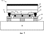
Фиг.1 - сечение одного варианта осуществления тонкого светоизлучающего диода бокового излучения, установленного на подложке;Figure 1 is a cross section of one embodiment of a thin light emitting diode side radiation mounted on a substrate;
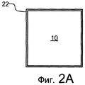
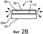
Фиг.2А и 2В иллюстрируют виды сверху и сбоку, соответственно, светоизлучающего диода на подложке;2A and 2B illustrate top and side views, respectively, of a light emitting diode on a substrate;
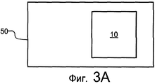
Фиг.3А и 3В иллюстрируют виды сверху и сбоку, соответственно, светоизлучающего диода на большой подложке;3A and 3B illustrate top and side views, respectively, of a light emitting diode on a large substrate;
Фиг.4 показывает вид сбоку светоизлучающего диода на большой подложке с отражателем, который перенаправляет излучаемый свет бокового излучения в направленный вперед свет;Figure 4 shows a side view of a light emitting diode on a large substrate with a reflector that redirects the emitted light of the side radiation into the forward light;
Фиг.5 показывает вид сбоку светоизлучающего диода и отражателя согласно варианту осуществления настоящего изобретения;5 shows a side view of a light emitting diode and a reflector according to an embodiment of the present invention;
Фиг.6 показывает вид сбоку светоизлучающего диода и линзы согласно другому варианту осуществления настоящего изобретения;6 shows a side view of a light emitting diode and lens according to another embodiment of the present invention;
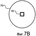
Фиг. 7А и 7В иллюстрируют виды сверху линзы из Фиг.6 квадратной и круговой конфигураций;FIG. 7A and 7B illustrate top views of the lens of FIG. 6 in a square and circular configuration;
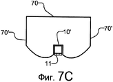
Фиг.7С иллюстрирует вид сверху светоизлучающего диода бокового излучения с тремя сторонами и линзы, используемой вместе с ним;Fig. 7C illustrates a top view of a three-sided side-emitting light emitting diode and a lens used with it;
Фиг.8 иллюстрирует вид сверху светоизлучающего диода с частью линзы, имеющей входные поверхности с вертикально ориентированными изменяющимися наклонными стенками для улучшения углового смешения света;Fig. 8 illustrates a top view of a light emitting diode with a portion of a lens having input surfaces with vertically oriented varying inclined walls to improve angular light mixing;
Фиг. 9А-9С иллюстрируют варианты осуществления изготовления линзы с использованием литой выводной рамки;FIG. 9A-9C illustrate embodiments of manufacturing a lens using a cast lead frame;
Фиг. 9D и 9Е иллюстрируют вариант осуществления сформированной подложки;FIG. 9D and 9E illustrate an embodiment of a formed substrate;
Фиг.10 иллюстрирует вид сверху устройства задней подсветки, включающего в себя распределение множества светоизлучающих диодов;Figure 10 illustrates a top view of a backlight device including a distribution of a plurality of light emitting diodes;
Фиг.11 - сечение части устройства задней подсветки из Фиг.10;11 is a sectional view of a portion of the backlight device of FIG. 10;
Фиг.12 - частичное сечение устройства задней подсветки другого типа с оптическими ячейками;12 is a partial cross section of another type of backlight device with optical cells;
Фиг.13 иллюстрирует вид сверху устройства задней подсветки из Фиг.12; иFig. 13 illustrates a top view of the backlight device of Fig. 12; and
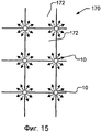
Фиг. 14 и 15 иллюстрируют множество ячеек в устройстве задней подсветки, аналогичном устройству, показанному на Фиг.13, со светоизлучающими диодами, расположенными на границах между ячейками.FIG. 14 and 15 illustrate a plurality of cells in a backlight device similar to the device shown in FIG. 13, with light emitting diodes located at the boundaries between the cells.
Подробное описаниеDetailed description
Варианты осуществления настоящего изобретения охватывают низкопрофильные светоизлучающие диоды бокового излучения в сочетании с оптическими элементами, такими как отражатель, линза или коллимирующий элемент. Одним применением изобретения является тонкое устройство задней подсветки в жидкокристаллическом дисплее, но другие применения существуют и будут выявлены в свете настоящего раскрытия.Embodiments of the present invention encompass low-profile side-emitting light emitting diodes in combination with optical elements such as a reflector, lens, or collimating element. One application of the invention is a thin backlight device in a liquid crystal display, but other applications exist and will be identified in light of the present disclosure.
На Фиг.1 представлено сечение одного варианта осуществления тонкого светоизлучающего диода 10 бокового излучения, который включает в себя полупроводниковый светоизлучающий элемент 13, преобразующий длину волны элемент 30 и отражающую пленку 32. Светоизлучающий диод 10 бокового излучения установлен на подложке 22, которая установлена на печатной плате 28. Другие варианты осуществления тонких светоизлучающих диодов бокового излучения, которые можно использовать в исполнениях задней подсветки, можно найти в заявке США № 11/423419 под названием “Low profile side emitting LED”, поданной 9 июня 2006 г., автор Олег Щекин (Oleg Shchekin) и другие, переуступленной настоящему правопреемнику и включенной в эту заявку путем ссылки.Figure 1 shows a cross section of one embodiment of a thin side-emitting
В одном примере активный слой светоизлучающего диода 10 генерирует голубой свет. Светоизлучающий диод 10 формируют на исходной подложке для выращивания, такой как сапфировая, SiC или GaN. Обычно выращивают n-слой 12, за которым следует активный слой 14, за которым следует p-слой 16. Чтобы открыть участок нижележащего n-слоя 14, травят p-слой 16. После этого отражающие металлические электроды 18 (например, серебряные, алюминиевые или сплавные) формируют на поверхности светоизлучающего диода для контакта с n- и p-слоями. Когда диод смещают в прямом направлении, активный слой 14 излучает свет, длина волны которого определяется составом активного слоя (например, AlInGaN). Формирование таких светоизлучающих диодов является хорошо известным и нет необходимости описывать его более подробно. Дополнительные детали формирования светоизлучающих диодов описаны в патенте США № 6828596, автор Штайгервальд (Steigerwald) и другие, и в патенте США № 6876008, автор Бхат (Bhat) и другие, оба переуступлены настоящему правопреемнику и включены в эту заявку путем ссылки.In one example, the active layer of the
Затем полупроводниковый светоизлучающий элемент 13 устанавливают на подложку 22 методом перевернутого кристалла. Подложка 22 содержит металлические электроды 24, которые припаивают или приваривают ультразвуком к металлу 18 с помощью шариков 26 припоя. Кроме того, можно использовать соединения других видов. Шарики 26 припоя можно исключить, если сами электроды могут быть приварены ультразвуком.Then, the semiconductor
Электроды 24 подложки электрически соединены через сквозные отверстия с контактными столбиками на нижней стороне подложки 22, поэтому подложка 22 может быть установлена поверхностью на металлические столбики на печатной плате 28. Металлические дорожки на схемной плате 28 электрически соединяют контактные столбики с источником питания. Подложку 22 можно образовать из любого подходящего материала, такого как нитрид алюминия, керамика, кремний, алюминий и т.д. Если материал подложки является электропроводным, поверх материала подложки формируют изолирующий слой, а поверх изолирующего слоя формируют рисунок металлических электродов. Подложка 22 действует как механическая опора, обеспечивает электрическое соединение между хрупкими n- и p- электродами на кристалле светоизлучающего диода и источником питания и обеспечивает отвод тепла. Подложки хорошо известны.The
Чтобы сделать светоизлучающий диод 10 имеющим очень низкий профиль и чтобы предотвратить поглощение света подложкой для выращивания, подложку для выращивания удаляют, выполняя, например, химико-механическое полирование (CMP) или используя лазерный метод отслаивания, в котором лазер нагревает границу раздела GaN и подложки для выращивания до образования газа высокого давления, который отталкивает подложку от GaN. В одном варианте осуществления удаление подложки для выращивания выполняют после установки матрицы светоизлучающих диодов на пластину подложки и до разделения светоизлучающих диодов/подложек (например, распиливанием).To make the
После этого подложку для выращивания удаляют и преобразующий длину волны элемент 30, такой как планарный люминофорный слой 30, располагают на вершине светоизлучающего диода для преобразования длины волны голубого света, излучаемого из активного слоя 14. Люминофорный слой 30 можно сформировать заранее в виде керамического листа, присоединенного к слоям светоизлучающего диода, или люминофорные частицы можно осадить в виде тонкой пленки, например, электрофорезом. Люминофорный керамический лист может представлять собой спеченные люминофорные частицы или люминофорные частицы в прозрачном или просвечивающем связующем веществе, которое может быть органическим или неорганическим. Свет, излучаемый люминофорным слоем 30, при смешении с голубым (В) светом образует белый свет или другой требуемый свет. Люминофор может быть люминофором на основе алюмоиттриевого граната (АИГ, YAG), который создает желтый (Y) свет (Y+B=белый), или может быть комбинацией красного (R) люминофора и зеленого (G) люминофора (R+G+B=белый).After that, the growth substrate is removed and the wavelength-converting
В случае люминофора на основе алюмоиттриевого граната (то есть Се:YAG) цветовая температура белого света в значительной степени зависит от примеси Се в люминофоре, а также от толщины люминофорного слоя 30.In the case of a phosphor based on yttrium aluminum garnet (i.e., Ce: YAG), the color temperature of white light is largely dependent on the Ce impurity in the phosphor, as well as on the thickness of the
Затем поверх люминофорного слоя 30 формируют отражающую пленку 32. Отражающая пленка 32 является по существу параллельной верхней поверхности полупроводникового светоизлучающего элемента 13. Отражающая пленка 32 может быть зеркальной или рассеивающей. Зеркальный отражатель может быть распределенным брэгговским отражателем (РБО, DBR), образованным из органических или неорганических слоев. Зеркальный отражатель также может быть слоем алюминия или другого отражающего металла или комбинацией распределенного брэгговского отражателя и металла. Рассеивающий отражатель можно сформировать из металла, осаждаемого на шероховатую поверхность, или из рассеивающего материала, такого как подходящая белая краска или золь-гель раствор с TiO2 в силиконе. Кроме того, люминофорный слой 30 способствует рассеянию света, что повышает эффективность выхода света. В другом варианте осуществления отражатель расположен на расстоянии от светоизлучающего диода, как, например, отражатель, поддерживаемый волноводом поверх активного слоя, что приводит к тому, что светоизлучающий диод по-прежнему является светоизлучающим диодом бокового излучения, поскольку небольшое количество (например, до 10%) прямого света выходит из устройства задней подсветки над светоизлучающим диодом.Then, a
Хотя линзы с боковым излучением иногда используют для отклонения всего света, излучаемого с верхней поверхности светоизлучающего диода, в круговую диаграмму бокового излучения, такие линзы во много раз толще самого светоизлучающего диода и непригодны для сверхтонкого устройства обратной подсветки или других применений, в которых вертикальная высота является ограниченной.Although lateral radiation lenses are sometimes used to divert all the light emitted from the top surface of a light emitting diode into a circular side radiation pattern, such lenses are many times thicker than the light emitting diode itself and are unsuitable for an ultra-thin backlight device or other applications in which the vertical height is limited.
Обработку полупроводниковых слоев светоизлучающего диода можно производить до или после установки светоизлучающего диода на подложку 22.The processing of the semiconductor layers of the light emitting diode can be performed before or after installing the light emitting diode on the
Наибольшее количество света, излучаемого активным слоем 14, излучается через стороны светоизлучающего диода непосредственно или излучается через стороны после одного или нескольких внутренних отражений. Если верхний отражатель 32 является очень тонким, некоторая часть света может просачиваться через верхний отражатель 32.The largest amount of light emitted by the
В одном варианте осуществления подложка 22 имеет толщину около 380 микрон, полупроводниковые слои имеют общую толщину около 5 микрон, люминофорный слой 30 имеет толщину около 200 микрон и отражающая пленка 32 имеет толщину около 150 микрон, так что толщина светоизлучающего диода с добавлением толщины подложки составляет меньше чем 1 мм. Конечно, светоизлучающий диод 10 может быть изготовлен более толстым. Длина каждой стороны светоизлучающего диода обычно составляет меньше чем 1 мм, например, длина стороны может быть 0,6 мм; однако можно использовать сторону длиной 1,0 мм, например, для применений, требующих более высокой мощности.In one embodiment, the
Когда светоизлучающие диоды бокового излучения с перевернутым кристаллом используют в системах освещения, обеспечивается ряд преимуществ. Применение светоизлучающих диодов бокового излучения с перевернутым кристаллом для задней подсветки позволяет использовать более тонкие волноводы, меньшее количество светоизлучающих диодов, при этом обеспечиваются лучшая равномерность освещения и более высокая эффективность вследствие лучшего соединения света в волноводе.When the inverted crystal side-emitting light emitting diodes are used in lighting systems, a number of advantages are provided. The use of side-emitted side-emitting light emitting diodes for backlighting allows the use of thinner waveguides, fewer light emitting diodes, while providing better uniformity of illumination and higher efficiency due to better light coupling in the waveguide.
В другом варианте осуществления светоизлучающего диода (не показанного) отражающий материал может быть сформирован поверх одной или нескольких сторон люминофорного слоя, перпендикулярно к полупроводниковым слоям светоизлучающего диода. В таком случае свет излучается через непокрытые стороны люминофорного слоя, после чего может входить в волновод устройства задней подсветки. Любой светоизлучающий диод, который излучает свет преимущественно в пределах узкой зоны и/или угла между верхней и нижней поверхностями светоизлучающего диода, в этом раскрытии считается светоизлучающим диодом бокового излучения.In another embodiment of a light emitting diode (not shown), a reflective material may be formed over one or more sides of the phosphor layer, perpendicular to the semiconductor layers of the light emitting diode. In this case, light is emitted through the uncovered sides of the phosphor layer, after which it can enter the waveguide of the backlight device. Any light emitting diode that emits light mainly within a narrow zone and / or angle between the upper and lower surfaces of the light emitting diode is considered to be a side emitting light emitting diode in this disclosure.
На Фиг. 2А и 2В показаны соответствующие виды сверху и сбоку светоизлучающего диода 10 с подложкой 22. Как можно видеть на Фиг.2А, длина сторон светоизлучающего диода 10 приблизительно такая же, как и сторон подложки 22. В идеальном случае светоизлучающий диод 10 и подложка 22 должны иметь одинаковые горизонтальные размеры (или подложка 22 должна быть меньше), но на практике, вследствие необходимости разрезать подложку 22 без повреждения светоизлучающего диода 10, подложка 22 продолжается по горизонтали за пределы светоизлучающего 10 диода на расстояние от 5 мкм до 150 мкм вдоль всех светоизлучающих краев светоизлучающего диода 10. Как показано на Фиг.2В, в случае нахождения края 22а подложки 22 вблизи светоизлучающего края светоизлучающего диода 10 подложка 22 не является препятствием для света, излучаемого светоизлучающим диодом 10 по горизонтальному направлению, показанному стрелками.In FIG. 2A and 2B show respective top and side views of the
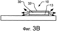
В отличие от этого на Фиг. 3А и 3В показаны соответствующие виды сверху и сбоку светоизлучающего диода 10 с большей подложкой 50. Как можно видеть, подложка 50 продолжается по горизонтали за пределы светоизлучающего диода 10 на относительно большую величину, например больше чем 150 мкм. На Фиг.3В показано, каким образом подложка 50 препятствует распространению значительного количества света, излучаемого светоизлучающим диодом 10, например света, излучаемого по нисходящей траектории. Хотя вблизи края большой подложки 50 можно помещать одну, две или даже три светоизлучающие стороны светоизлучающих диодов 10, свет, излучаемый с по меньшей мере одной стороны светоизлучающего диода 10, будет частично блокироваться подложкой 50. Кроме того, при наличии диода подавления переходного напряжения (TVS), установленного на подложке 50, будет блокироваться дополнительный свет.In contrast to FIG. 3A and 3B show respective top and side views of the
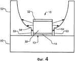
На Фиг.4 показана другая проблема, связанная с использованием большой подложки 50. На Фиг.4 показан вид сбоку светоизлучающего диода 10 на большой подложке 50 с оптическим элементом в виде отражателя 52, который перенаправляет свет бокового излучения в направленный вперед свет. Светоизлучающий диод 10, то есть полупроводниковый светоизлучающий элемент 13, преобразующий длину волны элемент 30 и отражающий слой 32, имеет вертикальную высоту меньше чем 4 мм. Вследствие практических проблем формования, связанных с конфигурацией «острого края» на основании 53 отражателя 52, основание 53 является относительно большим по сравнению с вертикальной высотой светоизлучающего диода 10. Поэтому нижний край 54 отражателя 52 оказывается расположенным между активным слоем 14 и отражающей пленкой 32, вследствие чего значительная часть светоизлучающей боковой стенки светоизлучающего диода 10 блокируется основанием 53 отражателя 52.Figure 4 shows another problem associated with the use of a
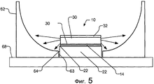
На Фиг.5 показан вариант осуществления, в котором светоизлучающий диод 10 установлен на подложке 22 вместе с оптическим элементом в виде отражателя 62, который аналогичен отражателю, показанному на Фиг.4, но не установлен на подложке 22. Отражатель 62 может быть установлен на печатной плате 28 (показанной на Фиг.1). В качестве варианта отражатель 62 может быть частью литой выводной рамки 68. Литую выводную рамку 68 можно изготовить обычным способом, например, из структурированных проводящих материалов, таких как медь. Литье пластика под давлением осуществляют вокруг проводящего материала, чтобы образовать литую выводную рамку, и также осуществляют формование, чтобы образовать оптический элемент, например отражатель 62. Внутренние поверхности отражателя 62 можно покрыть отражающим покрытием, например, алюминиевым или серебряным.Figure 5 shows an embodiment in which the
Отражатель 62 перенаправляет свет бокового излучения в направленный вперед свет, например, в конструкции вспышки фотоаппарата. Как должно быть видно на Фиг.5, нижний край 64 отражателя 62 расположен ниже верхней поверхности 22top подложки 22. В одном варианте осуществления нижний край 64 отражателя расположен на такой же вертикальной высоте, что и верхняя поверхность 22top подложки 22. В другом варианте осуществления нижний край 64 может быть расположен на уровне или ниже активного слоя 14. В качестве варианта нижний край 64 может быть расположен на уровне или ниже нижней поверхности 30bottom люминофорного слоя 30, который излучает наибольшую часть света бокового излучения. Таким образом, область светоизлучающей боковой стенки светоизлучающего диода 10, например, между активной областью 14 и нижней поверхностью отражающего слоя 32 полностью расположена в пределах области входа света отражателя 62 так, что свет, излучаемый от боковой стенки, не блокируется основанием 63 отражателя 62.A
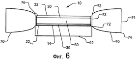
На Фиг.6 показан другой вариант осуществления, в котором светоизлучающий диод 10 установлен на подложке 22 вместе с оптическим элементом в виде линзы 70, оптически связанной со стороной светоизлучающего диода 10. Линза 70 представляет собой коллимирующую оптику, которая коллимирует свет бокового излучения в горизонтальной плоскости, который может использоваться для задней подсветки. На Фиг. 7А и 7В показаны виды сверху линзы 70 квадратной и круговой конфигураций вместе со светоизлучающим диодом 10. Как можно видеть, линза 70 связана с каждой светоизлучающей стороной светоизлучающего диода 10, и поэтому в настоящем варианте осуществления, где светоизлучающий диод 10 имеет четыре светоизлучающие стороны, линза 70 включает в себя четыре входные поверхности, связанные с каждой стороной. При желании отдельные индивидуальные линзы для каждого отдельной светоизлучающей стороны могут быть объединены с образованием линзы 70.6 shows another embodiment in which the
На Фиг.7С показан вид сверху светоизлучающего диода 10', бокового излучения с тремя сторонами, и соответствующей линзы 70', используемой со светоизлучающим диодом 10'. Светоизлучающий диод 10' аналогичен светоизлучающему диоду 10 бокового излучения с четырьмя сторонами, но может включать в себя, например, отражающий слой 11 на одной стороне. Линзе 70' придают определенную форму для приема света с трех краевых светоизлучающих сторон, чтобы создавать большую расходимость света, например, ±90° в задней световой плоскости, и чтобы коллимировать свет, например, ±20° в ортогональном направлении. Криволинейная форма линзы 70' является такой, что она осуществляет отражение за счет полного внутреннего отражения света (ПВО) со всех углов от левой и правой сторон светоизлучающего диода 10' бокового излучения. Как известно в данной области техники, полное внутреннее отражение происходит в случае, когда угол падения, внутренний по отношению к среде, >asin(n2/n1), то есть >43,6° от n1=1,45 до n2 (например, 1,0 для воздуха). Линзу 70' приводят в оптический контакт с 3 боковыми излучающими поверхностями путем, например, переформования, или используют связующий материал между поверхностями бокового излучателя и линзы. Связующий материал, такой как силикон, можно нанести и образовать «фитиль» между линзой 70' и материалом бокового излучателя светоизлучающего диода 10'.Fig. 7C is a plan view of a light emitting diode 10 ', side radiation with three sides, and the corresponding lens 70' used with the light emitting diode 10 '. The
Линза 70, показанная на Фиг.6, включает в себя входную область 72, которая оптически связана со светоизлучающими сторонами светоизлучающего диода 10 для приема света бокового излучения. Входная область 72 представляет собой область линзы, которая принимает свет от светоизлучающего диода 10 и в этом варианте осуществления включает в себя верхний край 72top и нижний край 72bottom. Нижний край 72bottom расположен на такой же вертикальной высоте, что и верхняя поверхность 22top подложки 22. В другом варианте осуществления нижний край 64 может быть расположен на уровне или ниже активного слоя 14. Альтернативно, нижний край 72bottom может быть расположен на уровне или ниже нижней поверхности 30bottom люминофорного слоя 30, который излучает наибольшую часть света бокового излучения. Верхний край 72top расположен на уровне или выше нижней поверхности отражающей пленки 32. Поэтому область светоизлучающей боковой стенки светоизлучающего диода 10, например, между активной областью 14 и нижней поверхностью отражающего слоя 32, полностью расположена в пределах входной области 72 линзы 70, так что свет, излучаемый с боковых стенок, не блокируется.The
Линза 70 также включает в себя одну или несколько выходных поверхностей 74, через которые излучается горизонтально коллимированный свет. Как показано на Фиг.7А, когда линза 70 имеет квадратную форму, имеются четыре выходные поверхности 74, при этом на Фиг.7В показана круглая линза 70 с одной выходной поверхностью. Выходная поверхность 74 может иметь высоту, например, около 3 мм или меньше, так что ее можно использовать при эксплуатации тонкого устройства задней подсветки. Как показано на Фиг.6, нижний край 74bottom выходной поверхности 74 может быть расположен значительно ниже вертикальной высоты верхней поверхности 22top подложки 22. Такая конфигурация является невозможной при использовании большой подложки 50, такой как показана на Фиг.3А.
Линза 70 может быть полой с отражающими боковыми стенками или сплошной, образованной путем придания заданной формы оптически прозрачному материалу, такому как силикон, стекло или пластик. В таком случае боковые стенки сплошной линзы могут быть покрыты отражающим материалом. Когда линзу 70 образуют из сплошного материала, то при предположении наличия воздушного промежутка или материала с меньшим показателем преломления между светоизлучающим диодом 10 с боковым излучателем и линзой 70 свет будет преломляться к нормали плоских стенок входной поверхности 72 среды с более высоким показателем, что приводит к меньшей интенсивности света вблизи углов светоизлучающего диода 10 по сравнению с интенсивностью непосредственно перед боковыми сторонами светоизлучающего диода 10.
В одном варианте осуществления пространство между светоизлучающим диодом 10 и линзой 70 может быть заполнено материалом 76, таким как силикон, для повышения выхода света и для улучшения углового смешения света. Например, материалы с различными показателями преломления можно использовать для заполняющего материала 76 и линзы 70, чтобы получать заданное угловое смешение или расхождение света, когда свет входит в линзу 70.In one embodiment, the space between the
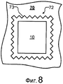
На Фиг.8 показан вид сверху светоизлучающего диода 10 с частью линзы 70, имеющей входные поверхности 72 с вертикально ориентированными углообразными стенками 73, которые также могут использоваться для улучшения углового смешения света внутри линзы 70. При изменении углов стенок 73 входной поверхности 72 свет, излучаемый светоизлучающим диодом 10, будет преломляться под другими углами, так что свет будет расходиться более равномерно. Поскольку свет коллимируют в горизонтальной плоскости, нет необходимости создавать горизонтально ориентированные углообразные стенки. Хотя на Фиг.8 показана пилообразная конфигурация входной поверхности 72, можно использовать другие конфигурации, например округлые или гребнеобразные формы. Форму боковых стенок также можно изменять с учетом распределения элементов вывода (extraction features), формируемых на нижней поверхности волновода, чтобы получать в наибольшей степени равномерный профиль яркости на световом выходе устройства задней подсветки.On Fig shows a top view of the
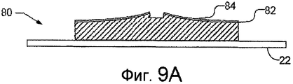
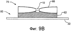
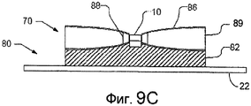
В одном варианте осуществления литую выводную рамку можно использовать вместе со светоизлучающим диодом 10 и линзой 70. На Фиг. 9А и 9В показан процесс изготовления светоизлучающего диода 10 с линзой 70 с литой выводной рамкой 80, согласно одному варианту осуществления. Литую выводную рамку 80 изготавливают из структурированного проводящего материала, при этом пластик или другой подходящий материал наносят литьем под давлением вокруг проводящего материала. Полученный литьем под давлением материал формуют для образования нижней поверхности 82 линзы 72 и покрывают отражающим слоем 84, например алюминиевым или серебряным. После этого светоизлучающий диод 10 может быть установлен на выводную рамку 80, а силикон осажден и отформован для образования линзы 70, показанной на Фиг.9В. Затем отражающий слой 86, например алюминиевый или серебряный, можно осадить поверх линзы 70. Отражающее покрытие не является необходимым или не используется, если конструкция коллиматорной линзы 70 основана на полном внутреннем отражении в материале линзы. В одном варианте осуществления, показанном на Фиг.9С, использован процесс двойного многокомпонентного переформования, в котором силиконовый материал 88 с первым показателем преломления, например 1,6, осаждают и формуют. Затем дополнительный силиконовый материал 89 с другим показателем преломления, например 1,3, осаждают и формуют для образования требуемой линзы 70. Как рассматривалось выше, для получения углового смешения света показатели преломления можно выбирать так, чтобы требуемое преломление происходило с указанным шагом. Кроме того, элементы, такие как элементы, показанные на Фиг.8, можно формовать в первом силиконовом материале 88, чтобы способствовать достижению заданного углового смешения света.In one embodiment, a cast lead frame may be used with the
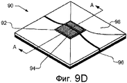
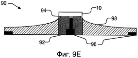
На Фиг. 9D и 9Е показаны общий вид и сечение (по линии А-А на Фиг.9D), соответственно, варианта осуществления сформированной подложки 90 с которой светоизлучающий диод 10 можно непосредственно устанавливать без необходимости в отдельной подложке 22. Сформированная подложка 90 включает в себя электропроводные n- и p-основания 92 и электроды 94, на которых (как показано на Фиг.9Е) установлен светоизлучающий диод 10. Сформированная подложка 90 также включает в себя рамку 96, изготовленную, например, из покрытой смолой меди, которая является неэлектропроводной и поэтому ее иногда называют подложкой с медной сердцевиной. Рамка 96 разделяет основания 92 и создает рамку для сформированного материала 98, который образует нижнюю поверхность коллиматорной линзы 70. Сформированным материалом 98 может быть, например, эпоксидный материал или пластик, или им может быть проводник, такой как медь, для улучшения рассеивания тепла. Как описывалось выше, отражающее покрытие можно осаждать поверх сформированного материала 98 с последующим многокомпонентным формованием линзы 70 (не показанной на Фиг. 9D и 9Е) с использованием, например, силикона. В одном варианте осуществления материал с низким коэффициентом преломления, например n=1,3, можно использовать для сформированного материала 98 или нанесения поверх сформированного материала 98, и материал с высоким показателем преломления, например n=1,6, можно использовать для линзы 70, так что в отличие от отражающего покрытия линза 70 может быть основана на полном внутреннем отражении.In FIG. 9D and 9E show a general view and section (along line AA in FIG. 9D), respectively, of an embodiment of the formed
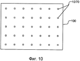
На Фиг.10 показан вид сверху устройства 100 обратной подсветки, включающего в себя распределение множества светоизлучающих диодов 10 с линзами 70. На Фиг.11 представлено сечение части устройства 100 обратной подсветки, сделанное поперек светоизлучающего диода 10. На Фиг.11 светоизлучающий диод 10 бокового излучения установлен на подложке 22 и схемной плате 28, а линза 70 введена в отверстие 34 в сплошном прозрачном волноводе 36. Для согласования с допусками на точность позиционирования между линзой 70 и стенками отверстия имеется небольшой воздушный промежуток, например 25 микрон. Волновод 36 может быть полым резонатором, формованным из пластика (например из полиметилметакрилата, PMMA) или другого подходящего материала. Зеркальная пленка 38 покрывает нижнюю поверхность и стороны волновода 36. Пленка 38 может быть пленкой с повышенным зеркальным отражением (ESR), поставляемой 3M Corporation, или белой рассеивающей пластиной внешнего рассеивания. Факультативно зеркальная пленка 38 или внешняя белая пластина закрывают боковые стороны. Вместо использования отражающей пленки волновод 36 можно закрепить в держателе с отражающими боковыми стенками.FIG. 10 is a plan view of a
Нижняя поверхность волновода 36 имеет большое количество небольших ямок 40 для рассеивания света по направлению вверх к задней поверхности светоизлучающего диода 42. Светоизлучающий диод 42 обычным образом избирательно управляет пикселами на экране дисплея. Ямки 40 можно создавать в процессе формования волновода 36 или их можно формировать травлением, пескоструйной обработкой, литографией или другим способом. Ямки 40 могут иметь любую форму, например призм или случайной шероховатости. Такие элементы иногда называют элементами вывода. В одном варианте осуществления, чтобы создать равномерное излучение света над верхней поверхностью волновода 36, плотность ямок 40 вблизи светоизлучающего диода 10 (где свет от светоизлучающего диода является более ярким) сделана меньшей, чем плотность ямок 40, отдаленных от светоизлучающего диода 10.The lower surface of the
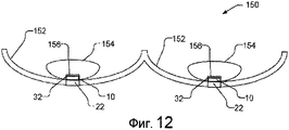
На Фиг.12 представлено частичное сечение другого типа устройства 150 задней подсветки, где каждый светоизлучающий диод 10 расположен в оптической ячейке 152. На Фиг.13 показан вид сверху устройства 150 задней подсветки. В этом варианте осуществления устройство 150 задней подсветки представляет собой структурированную рассеивающую пластину, которая может быть одномерной или двумерной и которая может быть использована для управления распределением света. Например, устройство 150 задней подсветки может быть микроячеистым отражающим листом, таким как МСРЕТ, производимый Furukawa Electric, или зеркальным отражателем с высокой отражательной способностью, или частично отражающим/рассеивающим элементом, который имеет высокую отражательную способность и высокую эффективность повторного использования. Часть света из каждой отражающей ячейки 152 может рассеиваться к соседним ячейкам, что позволяет смешивать свет от различных светоизлучающих диодов, и вследствие этого повышается равномерность света, а также создаются размытые границы между сегментами. Например, смешение света между ячейками может быть в пределах от 20% до 80% света, привнесенного из соседних ячеек.FIG. 12 is a partial sectional view of another type of
Светоизлучающие диоды 10 могут быть установлены в ячейках 152 вместе с дополнительными линзами 154, которые способствуют регулированию света бокового излучения. Как можно видеть, рассеивающий элемент 156 может быть расположен поверх отражающей пленки 32 светоизлучающего диода 10. Рассеивающий элемент 156 преобразует часть излучаемого вперед света, например света, который просачивается через отражающую пленку 32, в горизонтальном направлении. Рассеивающие элементы 156 обычно образуют при формовании линз. Альтернативно для образования элементов, которые перенаправляют свет от вертикального направления к горизонтальному направлению, можно использовать пескоструйную обработку, травление, трафаретную печать или другие способы.
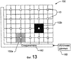
Как показано на Фиг.13, матрица светоизлучающих диодов 10 используется вместе со структурированной рассеивающей пластиной 150. В одном варианте осуществления каждый светоизлучающий светодиод 10 является независимо адресуемым по строке и столбцу для приема тока прямого смещения от источника тока 160 через соединитель 162. Поэтому, светоизлучающий светодиод 10, как показано в отражающей ячейке 152а, может снабжаться полным током, так что светоизлучающий диод может находиться во включенном состоянии в то время, когда светоизлучающий диод 10 в отражающей ячейке 152b не получает никакого тока, так что светоизлучающий диод будет находиться в выключенном состоянии. Например, является предпочтительным, чтобы задняя подсветка могла использоваться для изменения яркости выбранных участков экрана жидкокристаллического дисплея. Этот основанный на модульных ячейках способ можно использовать для двумерных систем уменьшения или повышения силы света, где задняя подсветка вырабатывает изображение с низким разрешением, позволяющее локально осуществлять значительное повышение коэффициента контраста (белое/черное) в сочетании с динамическим диапазоном жидкокристаллического дисплея, и снижает потребление мощности.As shown in FIG. 13, a matrix of
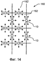
Хотя на Фиг.13 отражающие ячейки 152 показаны квадратными, должно быть понятно, что ячейки можно образовывать любой желаемой формы. Кроме того, элементы оформления, такие как форма оптики, форма нижнего отражателя и зеркальных и рассеивающих компонентов, расстояние до рассеивающего элемента и формирование рисунка рассеивателя, можно регулировать, чтобы по желанию корректировать равномерность или параметры расхождения света. Дополнительно можно использовать вариант размещения светоизлучающих диодов в ячейках. Например, на Фиг.14 показано множество ячеек 162 в устройстве 160 задней подсветки, аналогичном показанному на Фиг.13, за исключением того, что светоизлучающие диоды 10 расположены на границах между двумя соседними ячейками в отличие от светоизлучающих диодов, расположенных в центрах ячеек. Поэтому свет от каждого светоизлучающего диода 10 разделяется между двумя первичными ячейками, и в каждой ячейке имеется свет от четырех светоизлучающих диодов, посредством чего улучшается смешение света в ячейках. Аналогично этому на Фиг.15 показано множество ячеек 172 в устройстве 170 задней подсветки, которое аналогично устройству 160 обратной подсветки, показанному на Фиг.14, за исключением того, что светоизлучающие диоды расположены в углах каждой ячейки. В соответствии с этим свет от каждого светоизлучающего диода разделяется по четырем ячейкам. При желании светоизлучающий диод 10 можно расположить в центре каждой ячейки с тем, чтобы свет от пяти светоизлучающих диодов привносился в каждую ячейку 172.Although in FIG. 13 the
Хотя настоящее изобретение пояснено в связи с конкретными вариантами осуществления для рекомендательных целей, настоящее изобретение не ограничено ими. Различные варианты и модификации могут быть сделаны без отступления от объема изобретения. Поэтому сущность и объем прилагаемой формулы изобретения не подлежат ограничению приведенным выше описанием.Although the present invention has been explained in connection with specific embodiments for advisory purposes, the present invention is not limited to them. Various variations and modifications may be made without departing from the scope of the invention. Therefore, the nature and scope of the attached claims are not subject to limitation by the above description.
Claims (13)
нелазерный светоизлучающий диод (СИД) (10) бокового излучения, при этом светоизлучающий диод имеет множество светоизлучающих боковых стенок, при этом каждая светоизлучающая боковая стенка имеет верхний участок и нижний участок; в котором светоизлучающий диод излучает свет со своих светоизлучающих боковых стенок без использования линзы бокового излучения; и
оптический элемент (70), причем каждая из светоизлучающих боковых стенок светоизлучающего диода оптически связана с оптическим элементом, оптический элемент имеет нижний край, в котором свет, направляемый ниже нижнего края оптического элемента, не входит в оптический элемент; в котором нижний край оптического элемента расположен на уровне или ниже нижнего участка светоизлучающей боковой стенки,
подложку (90), на которой установлен светоизлучающий диод; и
первый силиконовый участок (98), сформированный поверх подложки и вокруг светоизлучающего диода, при этом верхняя поверхность первого силиконового участка имеет криволинейную форму, при этом криволинейная форма отлого поднимается вверх к светоизлучающему диоду и заканчивается ниже светоизлучающих боковых стенок светоизлучающего диода, при этом первый силиконовый участок имеет первый показатель преломления;
в котором оптический элемент (70) содержит второй силиконовый участок, сформированный поверх верхней поверхности первого силиконового участка и граничащий с ней, при этом второй силиконовый участок имеет второй показатель преломления, более высокий, чем первый показатель преломления, так что имеется полное внутреннее отражение света светоизлучающего диода на границе раздела первого силиконового участка и второго силиконового участка.1. A lighting device comprising:
a non-laser light emitting diode (LED) (10) of lateral radiation, wherein the light emitting diode has a plurality of light emitting side walls, with each light emitting side wall having an upper portion and a lower portion; wherein a light emitting diode emits light from its light emitting side walls without using a side radiation lens; and
an optical element (70), each of the light emitting side walls of the light emitting diode being optically coupled to the optical element, the optical element has a lower edge in which light directed below the lower edge of the optical element is not included in the optical element; in which the lower edge of the optical element is located at or below the lower portion of the light-emitting side wall,
a substrate (90) on which a light emitting diode is mounted; and
a first silicone portion (98) formed on top of the substrate and around the light emitting diode, wherein the upper surface of the first silicone portion has a curved shape, wherein the curved shape of the peeling rises up to the light emitting diode and ends below the light emitting side walls of the light emitting diode, wherein the first silicone portion has a first refractive index;
wherein the optical element (70) comprises a second silicone portion formed over and adjacent to the upper surface of the first silicone portion, wherein the second silicone portion has a second refractive index higher than the first refractive index, so that there is total internal reflection of light emitting light a diode at the interface of the first silicone portion and the second silicone portion.
полупроводниковый светоизлучающий прибор, имеющий контакты (94) на нижней поверхности, которые установлены на монтажной опоре (22) в конфигурации перевернутого кристалла, при этом полупроводниковый светоизлучающий прибор имеет верхнюю поверхность;
преобразующий длину волны материал (30) поверх верхней поверхности полупроводникового светоизлучающего прибора, при этом преобразующий длину волны материал имеет верхнюю поверхность и боковые стенки, которые являются боковыми стенками бокового излучения;
отражатель (32) на верхней поверхности преобразующего длину волны материала и являющийся, по существу, параллельным верхней поверхности полупроводникового светоизлучающего прибора, так что, по существу, весь свет, падающий на отражатель, перенаправляется обратно в преобразующий длину волны материал.9. The device according to claim 7, in which the light emitting diode contains:
a semiconductor light emitting device having contacts (94) on a lower surface that are mounted on a mounting support (22) in an inverted crystal configuration, wherein the semiconductor light emitting device has an upper surface;
a wavelength converting material (30) on top of the upper surface of the semiconductor light emitting device, wherein the wavelength converting material has an upper surface and side walls that are side walls of the side radiation;
a reflector (32) on the upper surface of the wavelength-converting material and being substantially parallel to the upper surface of the semiconductor light emitting device, so that substantially all of the light incident on the reflector is redirected back to the wavelength-converting material.
Applications Claiming Priority (3)
| Application Number | Priority Date | Filing Date | Title |
|---|---|---|---|
| US11/840,129 US7652301B2 (en) | 2007-08-16 | 2007-08-16 | Optical element coupled to low profile side emitting LED |
| US11/840,129 | 2007-08-16 | ||
| PCT/IB2008/053277 WO2009022316A2 (en) | 2007-08-16 | 2008-08-14 | Optical element coupled to low profile side emitting led |
Publications (2)
| Publication Number | Publication Date |
|---|---|
| RU2010109737A RU2010109737A (en) | 2011-09-27 |
| RU2477546C2 true RU2477546C2 (en) | 2013-03-10 |
Family
ID=40139392
Family Applications (1)
| Application Number | Title | Priority Date | Filing Date |
|---|---|---|---|
| RU2010109737/28A RU2477546C2 (en) | 2007-08-16 | 2008-08-14 | Light-emitting diode for lateral radiation with silicone lens supported by curvilinear silicone section |
Country Status (8)
| Country | Link |
|---|---|
| US (1) | US7652301B2 (en) |
| EP (1) | EP2191521B1 (en) |
| JP (1) | JP5318100B2 (en) |
| KR (1) | KR101548388B1 (en) |
| CN (1) | CN101779302B (en) |
| RU (1) | RU2477546C2 (en) |
| TW (1) | TWI447941B (en) |
| WO (1) | WO2009022316A2 (en) |
Cited By (1)
| Publication number | Priority date | Publication date | Assignee | Title |
|---|---|---|---|---|
| RU2662799C2 (en) * | 2013-06-25 | 2018-07-31 | Филипс Лайтинг Холдинг Б.В. | Light-emitting module with curved prism sheet |
Families Citing this family (69)
| Publication number | Priority date | Publication date | Assignee | Title |
|---|---|---|---|---|
| US8080828B2 (en) * | 2006-06-09 | 2011-12-20 | Philips Lumileds Lighting Company, Llc | Low profile side emitting LED with window layer and phosphor layer |
| US9046634B2 (en) * | 2007-06-14 | 2015-06-02 | Philips Lumileds Lighting Company, Llc | Thin flash or video recording light using low profile side emitting LED |
| US7538359B2 (en) * | 2007-08-16 | 2009-05-26 | Philips Lumiled Lighting Company, Llc | Backlight including side-emitting semiconductor light emitting devices |
| TWI352438B (en) * | 2007-08-31 | 2011-11-11 | Huga Optotech Inc | Semiconductor light-emitting device |
| KR100901369B1 (en) * | 2007-11-19 | 2009-06-05 | 일진반도체 주식회사 | White light emitting diode chip and manufacturing method therof |
| EP2212930B1 (en) * | 2007-11-20 | 2018-02-21 | Philips Lighting Holding B.V. | Collimating light emitting apparatus |
| JP2012502471A (en) * | 2008-09-04 | 2012-01-26 | スリーエム イノベイティブ プロパティズ カンパニー | Light source with light blocking component |
| CN101971364B (en) | 2008-11-06 | 2013-05-15 | 松下电器产业株式会社 | Nitride semiconductor element and method for manufacturing the same |
| US8058639B2 (en) * | 2009-04-06 | 2011-11-15 | Panasonic Corporation | Nitride semiconductor element and method for production thereof |
| US8097894B2 (en) * | 2009-07-23 | 2012-01-17 | Koninklijke Philips Electronics N.V. | LED with molded reflective sidewall coating |
| KR101112430B1 (en) * | 2009-12-21 | 2012-02-22 | 광전자 주식회사 | Light emitting chip and the method of the same, Optical device package and the method of the same |
| EP2479807B1 (en) * | 2009-12-25 | 2014-06-18 | Panasonic Corporation | Nitride semiconductor light emitting diode |
| CN102116441A (en) * | 2010-01-06 | 2011-07-06 | 奇菱科技股份有限公司 | Backlight module and light source component thereof |
| WO2011107928A1 (en) * | 2010-03-02 | 2011-09-09 | Koninklijke Philips Electronics N.V. | Led with transparent package |
| JP2011233650A (en) * | 2010-04-26 | 2011-11-17 | Toshiba Corp | Semiconductor light-emitting device |
| CN102339923A (en) * | 2010-07-28 | 2012-02-01 | 展晶科技(深圳)有限公司 | Light emitting diode (LED) chip |
| JP5178796B2 (en) * | 2010-09-10 | 2013-04-10 | 三菱電機株式会社 | Light emitting device and lighting device |
| TWI466346B (en) * | 2010-10-19 | 2014-12-21 | Advanced Optoelectronic Tech | Flip chip led package structure |
| JP5472031B2 (en) * | 2010-10-21 | 2014-04-16 | 日亜化学工業株式会社 | Light emitting device and manufacturing method thereof |
| US9351348B2 (en) * | 2010-10-27 | 2016-05-24 | Koninklijke Philips N.V. | Laminate support film for fabrication of light emitting devices and method of fabrication |
| KR20140023254A (en) * | 2010-11-05 | 2014-02-26 | 시노이아 테크놀로지스 리미티드 | A cosmetic applicator with sponge to absorb substance and to prevent leakage thereof |
| WO2012066461A1 (en) * | 2010-11-19 | 2012-05-24 | Koninklijke Philips Electronics N.V. | Islanded carrier for light emitting device |
| US20120217862A1 (en) * | 2010-12-24 | 2012-08-30 | Panasonic Corporation | Light bulb shaped lamp and lighting apparatus |
| CN102916105A (en) * | 2011-08-03 | 2013-02-06 | 宁波瑞昀光电照明科技有限公司 | LED lamp packaging enclosure structure |
| JP2013038115A (en) | 2011-08-04 | 2013-02-21 | Koito Mfg Co Ltd | Light wavelength conversion unit |
| JP5811770B2 (en) * | 2011-10-28 | 2015-11-11 | 日亜化学工業株式会社 | Light emitting device and manufacturing method thereof |
| KR101960373B1 (en) * | 2012-03-29 | 2019-03-20 | 엘지디스플레이 주식회사 | Back light assembly and liquid crystal display device using the same |
| JP5962904B2 (en) | 2012-04-26 | 2016-08-03 | パナソニックIpマネジメント株式会社 | Light source device and projection display device including the light source device |
| JP6089686B2 (en) | 2012-12-25 | 2017-03-08 | 日亜化学工業株式会社 | Light emitting device |
| US20150340566A1 (en) * | 2013-01-10 | 2015-11-26 | Koninklijke Philips N.V. | Led with shaped growth substrate for side emission |
| US8975659B2 (en) * | 2013-06-13 | 2015-03-10 | Cofan Usa, Inc. | Chip on board light emitting diode device having dissipation unit array |
| WO2015064883A1 (en) * | 2013-11-01 | 2015-05-07 | Seoul Semiconductor Co., Ltd. | Light source module and backlight unit having the same |
| JP6438648B2 (en) | 2013-11-15 | 2018-12-19 | 日亜化学工業株式会社 | Semiconductor light emitting device and manufacturing method thereof |
| KR20160106153A (en) * | 2014-01-08 | 2016-09-09 | 코닌클리케 필립스 엔.브이. | Deep molded reflector cup used as complete led package |
| CN105874615B (en) * | 2014-01-09 | 2020-01-03 | 亮锐控股有限公司 | Light emitting device with reflective sidewalls |
| JP6378532B2 (en) | 2014-05-08 | 2018-08-22 | 株式会社エンプラス | Light emitting device, surface light source device, and display device |
| JP6501052B2 (en) * | 2014-05-30 | 2019-04-17 | 日亜化学工業株式会社 | Light module, lighting device and display device |
| JP2015026851A (en) * | 2014-09-16 | 2015-02-05 | 株式会社小糸製作所 | Light emitting module |
| US9601668B2 (en) * | 2014-10-28 | 2017-03-21 | Nichia Corporation | Light emitting device |
| JP6537259B2 (en) * | 2014-12-05 | 2019-07-03 | シチズン電子株式会社 | Light emitting device |
| WO2016146658A1 (en) | 2015-03-16 | 2016-09-22 | Plessey Semiconductors Limited | Light emitting diode chip and a method for the manufacture of a light emitting diode chip |
| JP6470606B2 (en) | 2015-03-27 | 2019-02-13 | 株式会社エンプラス | Light emitting device, surface light source device, and display device |
| EP3308073B1 (en) * | 2015-06-09 | 2022-03-09 | Lumileds LLC | Headlight module |
| KR101685092B1 (en) * | 2015-11-06 | 2016-12-12 | 순천대학교 산학협력단 | Edge light emitting diode and method for manufacturing the same |
| JP6665690B2 (en) * | 2016-05-31 | 2020-03-13 | 日亜化学工業株式会社 | Lighting equipment |
| KR20180000976A (en) * | 2016-06-24 | 2018-01-04 | 서울반도체 주식회사 | Light emitting diode package |
| US10274168B2 (en) | 2016-07-20 | 2019-04-30 | Nichia Corporation | Light emitting device |
| JP6902838B2 (en) * | 2016-09-08 | 2021-07-14 | 晶元光電股▲ふん▼有限公司Epistar Corporation | Sheet for coating optical semiconductor devices |
| JP6985622B2 (en) * | 2016-12-26 | 2021-12-22 | 日亜化学工業株式会社 | Light emitting device and integrated light emitting device |
| JP6868388B2 (en) | 2016-12-26 | 2021-05-12 | 日亜化学工業株式会社 | Light emitting device and integrated light emitting device |
| JP6575507B2 (en) | 2016-12-28 | 2019-09-18 | 日亜化学工業株式会社 | Light emitting device and integrated light emitting device |
| TWI636595B (en) * | 2017-03-30 | 2018-09-21 | 宏齊科技股份有限公司 | Light emitting device |
| FR3064531B1 (en) * | 2017-03-31 | 2019-04-05 | Saint-Gobain Glass France | GLAZING LIGHTING. |
| TWI793203B (en) * | 2017-10-26 | 2023-02-21 | 晶元光電股份有限公司 | Light-emitting device |
| JP6870592B2 (en) * | 2017-11-24 | 2021-05-12 | 豊田合成株式会社 | Light emitting device |
| US11184967B2 (en) | 2018-05-07 | 2021-11-23 | Zane Coleman | Angularly varying light emitting device with an imager |
| US10816939B1 (en) | 2018-05-07 | 2020-10-27 | Zane Coleman | Method of illuminating an environment using an angularly varying light emitting device and an imager |
| KR20190133878A (en) | 2018-05-24 | 2019-12-04 | 엘지이노텍 주식회사 | Lighting module and lighting apparatus |
| KR20200048310A (en) | 2018-10-29 | 2020-05-08 | 엘지디스플레이 주식회사 | Light emitting display apparatus |
| CN109343273A (en) * | 2018-11-23 | 2019-02-15 | 江苏新广联科技股份有限公司 | A kind of big beam angle Mini LED backlight mould group and preparation method thereof |
| US11271143B2 (en) | 2019-01-29 | 2022-03-08 | Osram Opto Semiconductors Gmbh | μ-LED, μ-LED device, display and method for the same |
| US11610868B2 (en) * | 2019-01-29 | 2023-03-21 | Osram Opto Semiconductors Gmbh | μ-LED, μ-LED device, display and method for the same |
| US11156759B2 (en) | 2019-01-29 | 2021-10-26 | Osram Opto Semiconductors Gmbh | μ-LED, μ-LED device, display and method for the same |
| US11538852B2 (en) | 2019-04-23 | 2022-12-27 | Osram Opto Semiconductors Gmbh | μ-LED, μ-LED device, display and method for the same |
| JP2020188073A (en) * | 2019-05-10 | 2020-11-19 | シャープ株式会社 | Led light source substrate and lighting device |
| CN110400519A (en) | 2019-07-29 | 2019-11-01 | 京东方科技集团股份有限公司 | Backlight module and preparation method thereof, display device |
| JP7349294B2 (en) * | 2019-08-29 | 2023-09-22 | 株式会社ジャパンディスプレイ | LED module and display device |
| CN113703223B (en) * | 2021-08-18 | 2022-07-26 | Tcl华星光电技术有限公司 | Backlight module, preparation method thereof and display panel |
| US11852917B2 (en) | 2021-08-18 | 2023-12-26 | Tcl China Star Optoelectronics Technology Co., Ltd. | Backlight module and preparation method therefor, and display panel |
Citations (6)
| Publication number | Priority date | Publication date | Assignee | Title |
|---|---|---|---|---|
| RU2142661C1 (en) * | 1998-12-29 | 1999-12-10 | Швейкин Василий Иванович | Injection non-coherent light source |
| RU2207663C2 (en) * | 2001-07-17 | 2003-06-27 | Ооо Нпц Оэп "Оптэл" | Light-emitting diode |
| US20030189830A1 (en) * | 2001-04-12 | 2003-10-09 | Masaru Sugimoto | Light source device using led, and method of producing same |
| RU2267188C2 (en) * | 2003-06-23 | 2005-12-27 | Федорова Галина Владимировна | Light-emitting diode semiconductor device in casing for surface wiring |
| JP2006032349A (en) * | 2004-07-16 | 2006-02-02 | Osram Sylvania Inc | Molded light emitting diode light source |
| US20070085105A1 (en) * | 2005-10-18 | 2007-04-19 | Goldeneye, Inc. | Light emitting diode and side emitting lens |
Family Cites Families (14)
| Publication number | Priority date | Publication date | Assignee | Title |
|---|---|---|---|---|
| US6156028A (en) * | 1994-03-21 | 2000-12-05 | Prescott; Marvin A. | Method and apparatus for therapeutic laser treatment of wounds |
| TW383508B (en) * | 1996-07-29 | 2000-03-01 | Nichia Kagaku Kogyo Kk | Light emitting device and display |
| US5813752A (en) * | 1997-05-27 | 1998-09-29 | Philips Electronics North America Corporation | UV/blue LED-phosphor device with short wave pass, long wave pass band pass and peroit filters |
| JP4432275B2 (en) * | 2000-07-13 | 2010-03-17 | パナソニック電工株式会社 | Light source device |
| US6679621B2 (en) * | 2002-06-24 | 2004-01-20 | Lumileds Lighting U.S., Llc | Side emitting LED and lens |
| US6903380B2 (en) * | 2003-04-11 | 2005-06-07 | Weldon Technologies, Inc. | High power light emitting diode |
| JP2004335880A (en) * | 2003-05-09 | 2004-11-25 | Toshiba Lighting & Technology Corp | Light emitting device |
| JP2005039193A (en) * | 2003-06-26 | 2005-02-10 | Kyocera Corp | Package for housing light emitting element, light emitting device, and luminair |
| JP4288481B2 (en) * | 2003-10-02 | 2009-07-01 | シチズン電子株式会社 | Light emitting diode |
| JP2005243973A (en) * | 2004-02-26 | 2005-09-08 | Kyocera Corp | Light-emitting device and luminaire |
| KR100688767B1 (en) * | 2004-10-15 | 2007-02-28 | 삼성전기주식회사 | Lens for LED light source |
| JP2006236770A (en) * | 2005-02-24 | 2006-09-07 | Sony Corp | Backlight device and liquid crystal display |
| US7375379B2 (en) * | 2005-12-19 | 2008-05-20 | Philips Limileds Lighting Company, Llc | Light-emitting device |
| JP2007184319A (en) * | 2006-01-04 | 2007-07-19 | Showa Denko Kk | Semiconductor light emitting device |
-
2007
- 2007-08-16 US US11/840,129 patent/US7652301B2/en active Active
-
2008
- 2008-08-14 RU RU2010109737/28A patent/RU2477546C2/en active
- 2008-08-14 WO PCT/IB2008/053277 patent/WO2009022316A2/en active Application Filing
- 2008-08-14 EP EP08807326.7A patent/EP2191521B1/en active Active
- 2008-08-14 JP JP2010520672A patent/JP5318100B2/en active Active
- 2008-08-14 KR KR1020107005840A patent/KR101548388B1/en active IP Right Grant
- 2008-08-14 CN CN2008801033486A patent/CN101779302B/en active Active
- 2008-08-15 TW TW097131403A patent/TWI447941B/en active
Patent Citations (6)
| Publication number | Priority date | Publication date | Assignee | Title |
|---|---|---|---|---|
| RU2142661C1 (en) * | 1998-12-29 | 1999-12-10 | Швейкин Василий Иванович | Injection non-coherent light source |
| US20030189830A1 (en) * | 2001-04-12 | 2003-10-09 | Masaru Sugimoto | Light source device using led, and method of producing same |
| RU2207663C2 (en) * | 2001-07-17 | 2003-06-27 | Ооо Нпц Оэп "Оптэл" | Light-emitting diode |
| RU2267188C2 (en) * | 2003-06-23 | 2005-12-27 | Федорова Галина Владимировна | Light-emitting diode semiconductor device in casing for surface wiring |
| JP2006032349A (en) * | 2004-07-16 | 2006-02-02 | Osram Sylvania Inc | Molded light emitting diode light source |
| US20070085105A1 (en) * | 2005-10-18 | 2007-04-19 | Goldeneye, Inc. | Light emitting diode and side emitting lens |
Cited By (1)
| Publication number | Priority date | Publication date | Assignee | Title |
|---|---|---|---|---|
| RU2662799C2 (en) * | 2013-06-25 | 2018-07-31 | Филипс Лайтинг Холдинг Б.В. | Light-emitting module with curved prism sheet |
Also Published As
| Publication number | Publication date |
|---|---|
| RU2010109737A (en) | 2011-09-27 |
| CN101779302A (en) | 2010-07-14 |
| JP5318100B2 (en) | 2013-10-16 |
| JP2010537400A (en) | 2010-12-02 |
| WO2009022316A2 (en) | 2009-02-19 |
| WO2009022316A3 (en) | 2009-09-03 |
| KR101548388B1 (en) | 2015-08-28 |
| EP2191521B1 (en) | 2018-10-10 |
| TW200929614A (en) | 2009-07-01 |
| US7652301B2 (en) | 2010-01-26 |
| CN101779302B (en) | 2012-05-30 |
| US20090045416A1 (en) | 2009-02-19 |
| KR20100061686A (en) | 2010-06-08 |
| EP2191521A2 (en) | 2010-06-02 |
| TWI447941B (en) | 2014-08-01 |
Similar Documents
| Publication | Publication Date | Title |
|---|---|---|
| RU2477546C2 (en) | Light-emitting diode for lateral radiation with silicone lens supported by curvilinear silicone section | |
| JP5936158B2 (en) | Thin edge backlight with LEDs optically coupled to the back surface | |
| KR101529473B1 (en) | Thin backlight using low profile side emitting leds | |
| US7626210B2 (en) | Low profile side emitting LED | |
| US20090046479A1 (en) | Thin Backlight Using Low Profile Side Emitting LED |
Legal Events
| Date | Code | Title | Description |
|---|---|---|---|
| PD4A | Correction of name of patent owner | ||
| PD4A | Correction of name of patent owner | ||
| PC41 | Official registration of the transfer of exclusive right |
Effective date: 20190111 |
|
| PD4A | Correction of name of patent owner |