RU2248647C2 - Thermal cell - Google Patents
Thermal cell Download PDFInfo
- Publication number
- RU2248647C2 RU2248647C2 RU2002132261/28A RU2002132261A RU2248647C2 RU 2248647 C2 RU2248647 C2 RU 2248647C2 RU 2002132261/28 A RU2002132261/28 A RU 2002132261/28A RU 2002132261 A RU2002132261 A RU 2002132261A RU 2248647 C2 RU2248647 C2 RU 2248647C2
- Authority
- RU
- Russia
- Prior art keywords
- layer
- thermocouple
- layers
- junction
- thermocouple according
- Prior art date
Links
Images
Classifications
-
- H—ELECTRICITY
- H10—SEMICONDUCTOR DEVICES; ELECTRIC SOLID-STATE DEVICES NOT OTHERWISE PROVIDED FOR
- H10N—ELECTRIC SOLID-STATE DEVICES NOT OTHERWISE PROVIDED FOR
- H10N10/00—Thermoelectric devices comprising a junction of dissimilar materials, i.e. devices exhibiting Seebeck or Peltier effects
- H10N10/80—Constructional details
-
- H—ELECTRICITY
- H10—SEMICONDUCTOR DEVICES; ELECTRIC SOLID-STATE DEVICES NOT OTHERWISE PROVIDED FOR
- H10N—ELECTRIC SOLID-STATE DEVICES NOT OTHERWISE PROVIDED FOR
- H10N10/00—Thermoelectric devices comprising a junction of dissimilar materials, i.e. devices exhibiting Seebeck or Peltier effects
- H10N10/10—Thermoelectric devices comprising a junction of dissimilar materials, i.e. devices exhibiting Seebeck or Peltier effects operating with only the Peltier or Seebeck effects
- H10N10/17—Thermoelectric devices comprising a junction of dissimilar materials, i.e. devices exhibiting Seebeck or Peltier effects operating with only the Peltier or Seebeck effects characterised by the structure or configuration of the cell or thermocouple forming the device
-
- H—ELECTRICITY
- H10—SEMICONDUCTOR DEVICES; ELECTRIC SOLID-STATE DEVICES NOT OTHERWISE PROVIDED FOR
- H10N—ELECTRIC SOLID-STATE DEVICES NOT OTHERWISE PROVIDED FOR
- H10N10/00—Thermoelectric devices comprising a junction of dissimilar materials, i.e. devices exhibiting Seebeck or Peltier effects
- H10N10/80—Constructional details
- H10N10/85—Thermoelectric active materials
- H10N10/851—Thermoelectric active materials comprising inorganic compositions
- H10N10/852—Thermoelectric active materials comprising inorganic compositions comprising tellurium, selenium or sulfur
-
- H—ELECTRICITY
- H10—SEMICONDUCTOR DEVICES; ELECTRIC SOLID-STATE DEVICES NOT OTHERWISE PROVIDED FOR
- H10N—ELECTRIC SOLID-STATE DEVICES NOT OTHERWISE PROVIDED FOR
- H10N10/00—Thermoelectric devices comprising a junction of dissimilar materials, i.e. devices exhibiting Seebeck or Peltier effects
- H10N10/80—Constructional details
- H10N10/85—Thermoelectric active materials
- H10N10/851—Thermoelectric active materials comprising inorganic compositions
- H10N10/855—Thermoelectric active materials comprising inorganic compositions comprising compounds containing boron, carbon, oxygen or nitrogen
-
- H—ELECTRICITY
- H01—ELECTRIC ELEMENTS
- H01L—SEMICONDUCTOR DEVICES NOT COVERED BY CLASS H10
- H01L2224/00—Indexing scheme for arrangements for connecting or disconnecting semiconductor or solid-state bodies and methods related thereto as covered by H01L24/00
- H01L2224/01—Means for bonding being attached to, or being formed on, the surface to be connected, e.g. chip-to-package, die-attach, "first-level" interconnects; Manufacturing methods related thereto
- H01L2224/42—Wire connectors; Manufacturing methods related thereto
- H01L2224/44—Structure, shape, material or disposition of the wire connectors prior to the connecting process
- H01L2224/45—Structure, shape, material or disposition of the wire connectors prior to the connecting process of an individual wire connector
- H01L2224/45001—Core members of the connector
- H01L2224/45099—Material
- H01L2224/451—Material with a principal constituent of the material being a metal or a metalloid, e.g. boron (B), silicon (Si), germanium (Ge), arsenic (As), antimony (Sb), tellurium (Te) and polonium (Po), and alloys thereof
- H01L2224/45138—Material with a principal constituent of the material being a metal or a metalloid, e.g. boron (B), silicon (Si), germanium (Ge), arsenic (As), antimony (Sb), tellurium (Te) and polonium (Po), and alloys thereof the principal constituent melting at a temperature of greater than or equal to 950°C and less than 1550°C
- H01L2224/45144—Gold (Au) as principal constituent
-
- H—ELECTRICITY
- H01—ELECTRIC ELEMENTS
- H01L—SEMICONDUCTOR DEVICES NOT COVERED BY CLASS H10
- H01L2224/00—Indexing scheme for arrangements for connecting or disconnecting semiconductor or solid-state bodies and methods related thereto as covered by H01L24/00
- H01L2224/01—Means for bonding being attached to, or being formed on, the surface to be connected, e.g. chip-to-package, die-attach, "first-level" interconnects; Manufacturing methods related thereto
- H01L2224/42—Wire connectors; Manufacturing methods related thereto
- H01L2224/47—Structure, shape, material or disposition of the wire connectors after the connecting process
- H01L2224/48—Structure, shape, material or disposition of the wire connectors after the connecting process of an individual wire connector
- H01L2224/484—Connecting portions
- H01L2224/48463—Connecting portions the connecting portion on the bonding area of the semiconductor or solid-state body being a ball bond
-
- H—ELECTRICITY
- H01—ELECTRIC ELEMENTS
- H01L—SEMICONDUCTOR DEVICES NOT COVERED BY CLASS H10
- H01L2224/00—Indexing scheme for arrangements for connecting or disconnecting semiconductor or solid-state bodies and methods related thereto as covered by H01L24/00
- H01L2224/01—Means for bonding being attached to, or being formed on, the surface to be connected, e.g. chip-to-package, die-attach, "first-level" interconnects; Manufacturing methods related thereto
- H01L2224/42—Wire connectors; Manufacturing methods related thereto
- H01L2224/47—Structure, shape, material or disposition of the wire connectors after the connecting process
- H01L2224/49—Structure, shape, material or disposition of the wire connectors after the connecting process of a plurality of wire connectors
- H01L2224/491—Disposition
- H01L2224/49105—Connecting at different heights
- H01L2224/49107—Connecting at different heights on the semiconductor or solid-state body
-
- H—ELECTRICITY
- H01—ELECTRIC ELEMENTS
- H01L—SEMICONDUCTOR DEVICES NOT COVERED BY CLASS H10
- H01L2224/00—Indexing scheme for arrangements for connecting or disconnecting semiconductor or solid-state bodies and methods related thereto as covered by H01L24/00
- H01L2224/01—Means for bonding being attached to, or being formed on, the surface to be connected, e.g. chip-to-package, die-attach, "first-level" interconnects; Manufacturing methods related thereto
- H01L2224/42—Wire connectors; Manufacturing methods related thereto
- H01L2224/47—Structure, shape, material or disposition of the wire connectors after the connecting process
- H01L2224/49—Structure, shape, material or disposition of the wire connectors after the connecting process of a plurality of wire connectors
- H01L2224/491—Disposition
- H01L2224/4918—Disposition being disposed on at least two different sides of the body, e.g. dual array
-
- H—ELECTRICITY
- H01—ELECTRIC ELEMENTS
- H01L—SEMICONDUCTOR DEVICES NOT COVERED BY CLASS H10
- H01L2924/00—Indexing scheme for arrangements or methods for connecting or disconnecting semiconductor or solid-state bodies as covered by H01L24/00
- H01L2924/30—Technical effects
- H01L2924/301—Electrical effects
- H01L2924/3025—Electromagnetic shielding
-
- Y—GENERAL TAGGING OF NEW TECHNOLOGICAL DEVELOPMENTS; GENERAL TAGGING OF CROSS-SECTIONAL TECHNOLOGIES SPANNING OVER SEVERAL SECTIONS OF THE IPC; TECHNICAL SUBJECTS COVERED BY FORMER USPC CROSS-REFERENCE ART COLLECTIONS [XRACs] AND DIGESTS
- Y10—TECHNICAL SUBJECTS COVERED BY FORMER USPC
- Y10S—TECHNICAL SUBJECTS COVERED BY FORMER USPC CROSS-REFERENCE ART COLLECTIONS [XRACs] AND DIGESTS
- Y10S257/00—Active solid-state devices, e.g. transistors, solid-state diodes
- Y10S257/93—Thermoelectric, e.g. peltier effect cooling
Abstract
Description
Изобретение относится к термоэлементу, по меньшей мере, с одним n-слоем и, по меньшей мере, одним р-слоем одного или нескольких примесных полупроводников, при этом n-слой (слои) и р-слой (слои) расположены таким образом, что образуют, по меньшей мере, один р-n- переход, причем, по меньшей мере, один n-слой и, по меньшей мере, один р-слой селективно контактируют электрически, градиент температур прилагается или снимается параллельно /х-направление/ граничному слою между, по меньшей мере, одним n- и р- слоем.The invention relates to a thermocouple with at least one n-layer and at least one p-layer of one or more impurity semiconductors, while the n-layer (s) and p-layer (s) are arranged so that form at least one pn junction, at least one n-layer and at least one p-layer selectively contact electrically, a temperature gradient is applied or removed in parallel / x-direction / boundary layer between at least one n and p layer.
Термоэлектрический эффект известен уже более чем 100 лет. Имеется большой спектр материалов, которые могут применяться для прямого преобразования градиента температур в электрический ток. Техническая реализация этого эффекта неизменно основывается по сей день на общей принципиальной конструкции /фиг.1/. Два различных металла /а, b/ или два полупроводника с различной /n- и р-/ примесью соединены одним, как правило, горячим концом /температура T1/, а с другого, как правило, холодного конца /температура Т2/ может сниматься ток /сопротивление R в качестве условного потребителя/. Такие термоэлементы известны, например, из публикаций ЕР 0969526 A1, JP 11195817 A, JP 10144969 A, JP 10022531, A, JP 10022530 A, JP 57-1276 (A), JP 07038158 A, JP 59-980 (A), JP 57-169283 (A), JP 4-63481 (А) и US 5009717, при этом частично между n- и р-слоем в зоне n-р-перехода встроен проводящий слой в виде поверхности контакта. Общим для всех этих термоэлементов является то, что р-n-переход образован лишь в небольшой зоне между n- и р-слоем, в то время как большая зона образована между n- и р-слоем в виде воздушного зазора или изолирующего слоя (JP-63481 /А/ и US 5009717).The thermoelectric effect has been known for over 100 years. There is a wide range of materials that can be used to directly convert the temperature gradient into electric current. The technical implementation of this effect is invariably based to this day on the general principle design / Fig. 1/. Two different metals / a, b / or two semiconductors with different / n- and p- / impurities are connected by one, usually the hot end / temperature T 1 /, and on the other, as a rule, the cold end / temperature T 2 / can withdraw current / resistance R as a conditional consumer /. Such thermocouples are known, for example, from the publications EP 0969526 A1, JP 11195817 A, JP 10144969 A, JP 10022531, A, JP 10022530 A, JP 57-1276 (A), JP 07038158 A, JP 59-980 (A), JP 57-169283 (A), JP 4-63481 (A) and US 5009717, while partially between the n and p-layer in the zone of the n-p junction is a conductive layer in the form of a contact surface. Common to all these thermoelements is that the pn junction is formed only in a small zone between the n- and p-layer, while the large zone is formed between the n- and p-layer in the form of an air gap or an insulating layer (JP -63481 / A / and US 5009717).
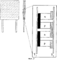
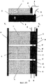
Для получения по возможности более эффективного преобразования градиента температур в электрический ток термоэлементы компонуются в виде единого модуля таким образом, что отдельные элементы электрически соединены последовательно, а термически - параллельно. Эти модули, в свою очередь, могут быть объединены в еще большие блоки /фиг.2/.To obtain the most efficient conversion of the temperature gradient into an electric current, the thermocouples are arranged as a single module in such a way that the individual elements are electrically connected in series and thermally in parallel. These modules, in turn, can be combined into even larger blocks (Fig. 2/).
Выбор используемых материалов осуществляется, следуя критерию максимально возможного кпд в заданном температурном интервале. Кпд характеризуется в целом показателем добротности Z=S2ρ k /S - коэффициент Зеебека или абсолютная дифференциальная термоэдс, ρ - удельное сопротивление, k - теплопроводность/. Высокий кпд достигается в материале высоким коэффициентом Зеебека при одновременно низком удельном сопротивлении и низкой теплопроводности.The choice of materials used is carried out following the criterion of the maximum possible efficiency in a given temperature range. Efficiency is characterized as a whole by the quality factor Z = S 2 ρ k / S is the Seebeck coefficient or absolute differential thermoelectric power, ρ is the resistivity, k is the thermal conductivity /. High efficiency is achieved in the material with a high Seebeck coefficient while at the same time low resistivity and low thermal conductivity.
Уровень техники имеет ряд недостатков: важные для термоэлектричества свойства материала /S - коэффициент Зеебека, ρ - удельное сопротивление, k - теплопроводимость/ лишь в очень незначительной степени поддаются воздействию независимо друг от друга. Эта взаимозависимость ограничивает возможный в настоящее время кпд примерно до 10-20%.The prior art has a number of disadvantages: material properties important for thermoelectricity / S is the Seebeck coefficient, ρ is resistivity, k is heat conductivity / can only be influenced to a very small extent independently from each other. This interdependence limits the currently possible efficiency to about 10-20%.
Изменение градиента температур согласно уровню техники практически едва ли оказывает воздействие на кпд, так как в традиционных термоэлементах, в связи с линейной зависимостью между термоэдс и перепадом температуры, играет роль лишь общий перепад температуры между горячей и холодной стороной.Changes in the temperature gradient according to the prior art hardly have any effect on the efficiency, since in traditional thermocouples, due to the linear relationship between the thermoelectric power and the temperature difference, only the general temperature difference between the hot and cold sides plays a role.
Попытки использования альтернативных вариантов, как, например, диодов /р-n-переходы/, таким образом, что одна сторона р-n-перехода теплее, чем другая сторона, показывают, разумеется, повышение кпд, однако, первоначальная концепция не получила значительного развития.Attempts to use alternative options, such as diodes / pn junctions /, in such a way that one side of the pn junction is warmer than the other side, of course, shows an increase in efficiency, however, the initial concept did not receive significant development .
Поэтому задача изобретения - создание усовершенствованного термоэлемента.Therefore, the objective of the invention is the creation of an improved thermocouple.
Согласно изобретению это достигается за счет того, что, по меньшей мере, один р-n- переход выполнен вдоль всего, предпочтительно наиболее длинной протяженности n-слоя (слоев) и р-слоя (слоев) и, таким образом, по существу вдоль их всего граничного слоя.According to the invention, this is achieved due to the fact that at least one pn junction is made along the entire, preferably the longest, length of the n-layer (s) and p-layer (s) and, thus, essentially along them the entire boundary layer.
Центральная, принципиально новая идея заключается в использовании, по меньшей мере, одного р-n-перехода, при этом градиент температур проходит вдоль р-n-перехода, имеющего соответственно продольную протяженность.The central, fundamentally new idea is to use at least one pn junction, while the temperature gradient passes along the pn junction, which has a corresponding longitudinal extent.
Согласно уровню техники р-n-переход создается лишь в небольшой контактной зоне с постоянной температурой, большей частью на стороне высокой температуры термоэлемента. Он служит лишь для улучшения электрического контакта между n- и р-легированными частями /слоями/. В отличие от этого согласно изобретению конструктивно предусмотрено, что, по меньшей мере, один р-n-переход образован по существу по всей протяженности n- и р-слоев, причем градиент температур приложен вдоль поверхности р-n-перехода. Тем самым создается перепад температур вдоль этого созданного в продольном направлении р-n-перехода между двумя концами пакета р-n-слоев, который приводит к тому, что кпд термоэлемента согласно изобретению значительно выше, чем согласно уровню техники, который не имеет градиента температур вдоль и внутри р-n-перехода. Более точный принцип действия основан на разнородном формировании модуляций потенциала в р-n-переходе при различных температурах, как это поясняется ниже на основе описания фигур.According to the prior art, the pn junction is created only in a small contact zone with a constant temperature, mostly on the high temperature side of the thermocouple. It serves only to improve electrical contact between n- and p-doped parts / layers /. In contrast, according to the invention, it is structurally provided that at least one pn junction is formed essentially over the entire length of the n and p layers, with a temperature gradient applied along the surface of the pn junction. This creates a temperature difference along this longitudinally created pn junction between the two ends of the pn layer stack, which leads to the fact that the efficiency of the thermocouple according to the invention is much higher than according to the prior art, which does not have a temperature gradient along and inside the pn junction. A more accurate principle of operation is based on the heterogeneous formation of modulations of the potential in the pn junction at different temperatures, as explained below based on the description of the figures.
Важным для принципа функционирования этого термоэлемента нового вида является селективное контактирование n- и р-слоя. Предпочтительно это может осуществляться либо вплавлением контактов и связанных с этим р-n-переходов, либо путем непосредственного контактирования отдельных слоев.Important for the principle of functioning of this new type of thermoelement is the selective contacting of the n and p layers. Preferably, this can be done either by fusing the contacts and the pn junctions associated with it, or by directly contacting the individual layers.
Другие преимущества и подробности изобретения поясняются более детально на основе следующего описания чертежей, на которых показано:Other advantages and details of the invention are explained in more detail based on the following description of the drawings, which show:
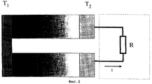
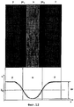
фиг.1 - принципиальная схема термоэлемента согласно уровню техники,figure 1 - schematic diagram of a thermocouple according to the prior art,
фиг.2 - термоэлектрический модуль согласно уровню техники,figure 2 - thermoelectric module according to the prior art,
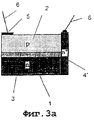
фиг.3 - принципиальная схема примера выполнения термоэлемента согласно предмету изобретения,figure 3 - schematic diagram of an example implementation of a thermocouple according to the subject invention,
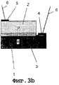
фиг.3а и 3b - другие примеры выполнения с различным селективным контактированием n-слоя или р-слоя,figa and 3b are other examples of execution with various selective contacting of the n-layer or p-layer,
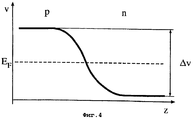
фиг.4 - потенциал v в зоне р-n-перехода в виде функции пространственной координаты z, перпендикулярной относительно p-n-перехода,4 is a potential v in the region of the pn junction in the form of a function of the spatial coordinate z perpendicular to the pn junction,
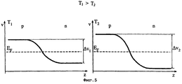
фиг.5 - две диаграммы согласно фиг.4, но с различными температурами T1 и Т2,figure 5 - two diagrams according to figure 4, but with different temperatures T 1 and T 2 ,
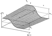
фиг.6 - схематическое трехмерное изображение к формированию градиента потенциала в n- и р-слое,6 is a schematic three-dimensional image to the formation of a potential gradient in the n - and p-layer,
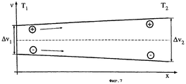
фиг.7 - схематическое изображение к возникновению амбиполярной диффузии,7 is a schematic illustration of the occurrence of ambipolar diffusion,
фиг.8 - диаграмма генерации электронно-дырочных пар,Fig.8 is a diagram of the generation of electron-hole pairs,
фиг.9 - рекомбинация электронно-дырочных пар за счет уменьшения модуляции потенциала,Fig.9 - recombination of electron-hole pairs by reducing modulation potential,
фиг.10 - благоприятная характеристика градиента температур по термоэлементу,figure 10 is a favorable characteristic of the temperature gradient by thermocouple,
фиг.11 - термоэлемент с изменением ширины на виде сверху и полученный таким образом градиент температур,11 - thermocouple with a change in width in a plan view and the temperature gradient thus obtained,
фиг.12 - пример выполнения с двумя р-n-переходами,12 is an exemplary embodiment with two pn junctions,
фиг.13 - конструкция термоэлектрического модуля из нескольких термоэлементов согласно изобретению иFig - design of a thermoelectric module of several thermocouples according to the invention and
фиг.14 - пример выполнения с высоколегированным n-, n-, р- и высоколегированным р-слоем.Fig. 14 is an exemplary embodiment with a highly alloyed n-, n-, p- and highly alloyed p-layer.
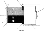
Принципиальная конструкция термоэлемента согласно изобретению показана на фиг.3: n-слой 1 и р-слой 2 образуют р-n-переход 3. Посредством контактов 4 и 5 n-слой 1 и р-слой 2 селективно контактируют и по цепи 6 сообщаются с оммическим потребителем 7 /R/. Градиент температур /T1 обозначает более высокую температуру, Т2 обозначает более низкую температуру/ прилагается в направлении, параллельном р-n-переходу 3 /х-направление/.The basic construction of the thermocouple according to the invention is shown in FIG. 3: the n-
На фиг.3а и 3b представлены примеры выполнения селективного контактирования n-слоя 1 или р-слоя 2. При этом толщина слоев представлена, по сравнению с протяженностью контакта в х-направлении, существенно большей /примерно коэффициент 100-1000/.On figa and 3b presents examples of selective contacting of the n-
На примере выполнения, представленном на фиг.3а, р-слой 2 контактирует непосредственно через поверхностно напыленный золотой контакт 5 /золотая проволока 6/. Для контактирования n-слоя используется вплавленный контакт 4’. Для РbТе может использоваться, например, индий для вплавленного контакта. Индий наносится на поверхность и в результате нагревания диффундирует в пакет из слоев. Легирование РbТе-индий относится к типу n+ /сильнолегированный/. Таким образом создается оммический контакт к n-слою 1 и р-n-переход к р-слою 2.In the exemplary embodiment shown in Fig. 3a, the p-
На примере исполнения, представленном на фиг.3b, осуществляется контактирование непосредственно n-слоя 1 и р-слоя 2, например, это возможно путем селективного протравливания покрывающего слоя.3b, the n-
Особое преимущество решения состоит в том, что используются нелинейные термические свойства р-n-переходов. Температура влияет как на энергию Ферми, так и /прежде всего/ на энергетическое распределение носителей заряда. В р-n-переходе вследствие этого происходит изменение модуляции потенциала. В данном случае модуляция потенциала описывает модуляцию потенциала для носителей заряда в полупроводниковых структурах, например, посредством р-n-перехода. Так, электронA particular advantage of the solution is that the nonlinear thermal properties of the pn junctions are used. Temperature affects both the Fermi energy and / primarily / the energy distribution of charge carriers. In the pn junction, as a result of this, a modulation of the potential occurs. In this case, the potential modulation describes the modulation of the potential for charge carriers in semiconductor structures, for example, by a pn junction. So, the electron
находится энергетически на более высоком потенциале в р-слое, чем в n-слое /для дырок, наоборот/, при этом разность этих двух потенциалов представляет собой модуляцию потенциала. Так как для каждой температуры существует уравновешенное значение для модуляции потенциала, то при изменении температуры происходит изменение модуляции потенциала.is energetically at a higher potential in the p-layer than in the n-layer / for holes, vice versa /, while the difference between these two potentials is a modulation of the potential. Since for each temperature there is a balanced value for the modulation of the potential, when the temperature changes, the modulation of the potential changes.
Благодаря градиенту температур, параллельно граничному слою между n- и р-слоем, происходит формирование латерального градиента потенциала в х-направлении и, вследствие этого, возникает амбиполярная диффузия носителей заряда и, вместе с ней, появляются уравнительные токи. Здесь амбиполярная диффузия носителей заряда означает диффузию в одном направлении разноименных носителей заряда в падении концентрации в одном направлении, как это описано с помощью фиг.7. Посредством селективных контактов /отдельные, не состоящие в проводящем соединении друг с другом контакты для n- и р-слоя/ этот внутренний уравнительный ток может быть отведен наружу. Этот процесс описывается коротко в следующих абзацах.Due to the temperature gradient parallel to the boundary layer between the n- and p-layer, the lateral gradient of the potential in the x-direction is formed and, as a result, ambipolar diffusion of charge carriers arises and, along with it, equalizing currents appear. Here, the ambipolar diffusion of charge carriers means the diffusion in one direction of opposite carriers in a drop in concentration in one direction, as described using Fig.7. By means of selective contacts (individual, non-conductive contacts to the n- and p-layer), this internal surge current can be diverted to the outside. This process is described briefly in the following paragraphs.
В качестве примера может быть рассмотрен узкополосный полупроводник РbТе /теллурид свинца/: изменение модуляции потенциала и, следовательно, максимальное теоретически используемое напряжение термоэлемента составляет примерно 20 мВ/100 К=2× 10⁻⁴ В/К (вольт/кельвин) и, таким образом, выше порядка величины коэффициента Зеебека в районе 1× 10⁻⁶ B/K. Благодаря конструкциям модулей из последовательно соединенных элементов достигаются более высокие напряжения.As an example, the narrow-band PbTe semiconductor / lead telluride / can be considered: a change in the modulation of the potential and, therefore, the maximum theoretically used thermoelement voltage is about 20 mV / 100 K = 2 × 10 -4 V / K (volt / kelvin) and, thus Thus, it is higher than the Seebeck coefficient in the region of 1 × 10 -6 B / K. Thanks to the design of the modules from series-connected elements, higher voltages are achieved.
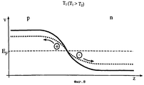
В термическом равновесии носители заряда распределяются (n и р) таким образом, что образуется суммарная энергия Ферми Ef /фиг.4/. Состояние энергии Ферми является функцией температуры и появляется модуляция Δ v потенциала, таким образом, модуляция потенциала также становится функцией температуры. Для двух различных температур T1 и Т2, где T1 выше Т2, возникает ситуация, подобная представленной на фиг.5. Р-n- переход с более высокой температурой T1 имеет меньшую модуляцию Δ v1 потенциала.In thermal equilibrium, the charge carriers are distributed (n and p) in such a way that the total Fermi energy E f / fig. 4 / is formed. The Fermi energy state is a function of temperature and a modulation Δ v of the potential appears, thus, the modulation of the potential also becomes a function of temperature. For two different temperatures T 1 and T 2 , where T 1 is higher than T 2 , a situation similar to that shown in FIG. 5 occurs. The Pn junction with a higher temperature T 1 has less modulation Δ v 1 potential.
Если в пакете из, по меньшей мере, одного n- и р-слоя градиент температур /T1>T1/ согласно изобретению существует параллельно граничному слою между n- и р-слоем в х-направлении, то зоны с различными температурами электрически контактируют. Так как при растущей температуре модуляция потенциала снижается, из этого следует, что соседние точки вдоль х-оси находятся на различных потенциалах. Фиг.6 представляет это схематически в 3-мерном изображении.If in a packet of at least one n- and p-layer a temperature gradient / T 1 > T 1 / according to the invention exists parallel to the boundary layer between the n and p-layer in the x-direction, then zones with different temperatures are electrically in contact . Since the potential modulation decreases with increasing temperature, it follows that neighboring points along the x-axis are at different potentials. 6 represents this schematically in a 3-dimensional image.
Пока нет тока, энергия Ферми Ef является горизонтальной на z-V-диаграмме /фиг.4/. Следовательно, создается соответствующий градиент потенциала в х-направлении как в р-, так и в n-слое. Градиенты потенциалов в обоих слоях противоположные, это значит, что носители зарядов в обоих слоях /электроны в n- и дырки в р-слое/ движутся в одном направлении. Это перемещение носителей зарядов называется амбиполярной диффузией. Фиг.7 представляет собой вид сбоку фиг.6 и поясняет этот процесс /дырки обозначены знаком +, а электроны знаком -/.As long as there is no current, the Fermi energy E f is horizontal in the zV diagram / Fig. 4/. Therefore, an appropriate potential gradient is created in the x-direction in both the p- and n-layer. The potential gradients in both layers are opposite, which means that the charge carriers in both layers / electrons in the n- and holes in the p-layer / move in the same direction. This movement of charge carriers is called ambipolar diffusion. Fig.7 is a side view of Fig.6 and explains this process / holes are indicated by +, and electrons by - /.
Следствием амбиполярной диффузии является то, что в зоне высокой температуры T1 пакета р-n-слоев происходит утечка носителей заряда и, следовательно, дефицит носителей заряда, экранирующий эффект на потенциал снижается и возрастает модуляция потенциала. В результате локальный р-n-переход больше не находится в тепловом равновесии и тепловая генерация электронно-дырочных пар преобладает над рекомбинацией /см. стрелки на фиг.8/.The consequence of ambipolar diffusion is that in the high temperature zone T 1 of the package of pn layers, charge carriers leak and, therefore, the deficit of charge carriers, the screening effect on the potential decreases and the modulation of the potential increases. As a result, the local pn junction is no longer in thermal equilibrium, and the thermal generation of electron-hole pairs prevails over recombination / cm. arrows in Fig. 8 /.
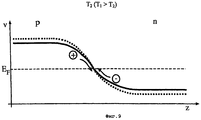
В зоне низкой температуры Т2 наблюдается переизбыток носителей заряда, который, в свою очередь, повышает экранирующее воздействие на локальный потенциал и приводит к снижению локальной модуляции потенциала по сравнению с тепловым равновесием. Это приводит к усиленной рекомбинации электронно-дырочных пар /см. стрелки на фиг.9/.In the zone of low temperature T 2 , an excess of charge carriers is observed, which, in turn, increases the screening effect on the local potential and leads to a decrease in the local modulation of the potential compared to thermal equilibrium. This leads to enhanced recombination of electron – hole pairs / cm. arrows in Fig.9 /.
В итоге получается, что в пакете слоев, по меньшей мере, с одним р-n-переходом протекает уравнительный ток до тех пор, пока зона пакета слоев остается более теплой, чем остальная поверхность, т.е. пока существует градиент температур параллельно граничному слою. Этот уравнительный ток передает тепло.As a result, it turns out that in the packet of layers with at least one pn junction, a surge current flows until the zone of the packet of layers remains warmer than the rest of the surface, i.e. while there is a temperature gradient parallel to the boundary layer. This surge current transfers heat.
В результате градиента температур параллельно граничному слою между n- и р-слоем имеют место, таким образом, генерация электронно-дырочных пар в области высокой температуры и рекомбинация этих пар в области низкой температуры с соответствующими уравнительными токами. Так как модуляция потенциала между n- и р-слоем изменяется в сравнении с тепловым равновесием, то между n- и р-слоем может быть измерено напряжение.As a result of the temperature gradient parallel to the boundary layer between the n- and p-layer, thus, the generation of electron-hole pairs in the high temperature region and the recombination of these pairs in the low temperature region with the corresponding equalizing currents take place. Since the modulation of the potential between the n- and p-layer varies in comparison with thermal equilibrium, a voltage can be measured between the n- and p-layer.
Поскольку модуляция потенциала между n- и р-слоем изменяется и протекают генерационные и рекомбинационные токи, для отвода токов наружу необходимо использовать контакты, контактирующие селективно лишь с n-слоем, и другие контакты, контактирующие селективно лишь с р-слоем. Селективность может осуществляться либо введением примесей /фиг.3а/ и созданием р-n-переходов, либо путем прямого контактирования /фиг.3, фиг.3b/ отдельных слоев.Since the potential modulation between the n and p layers changes and generation and recombination currents flow, it is necessary to use contacts contacting selectively only with the n layer and other contacts selectively contacting only the p layer to divert currents to the outside. Selectivity can be achieved either by introducing impurities (Fig. 3a) and creating pn junctions, or by direct contact (Fig. 3, Fig. 3b) of individual layers.
Принцип р-n-переходов имеет всеобщее применение, поэтому для термоэлектричества могут быть использованы все материалы, образующие р-n-переход.The principle of pn junctions has universal application, therefore, all materials forming a pn junction can be used for thermoelectricity.
Важные для термоэлектричества свойства материала /S коэффициент Зеебека, ρ - удельное сопротивление, k - теплопроводность/ поддаются воздействию лишь в очень незначительной мере независимо одно от другого. Представленный здесь новый принцип позволяет осуществлять латеральные изменения важных физических параметров в х-направлении, имеющие воздействие на элемент в целом, что открывает целый ряд новых возможностей для повышения кпд. К числу этих физических параметров относятся состав применяемого материала, введение примесей, толщина слоев, ширина и пр.Material properties important for thermoelectricity / S are the Seebeck coefficient, ρ is the resistivity, k is the thermal conductivity / can only be affected to a very insignificant extent independently of one another. The new principle presented here allows lateral changes in important physical parameters in the x-direction, having an effect on the element as a whole, which opens up a number of new possibilities for increasing efficiency. Among these physical parameters are the composition of the material used, the introduction of impurities, layer thickness, width, etc.
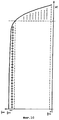
Характер градиента температур имеет влияние на кпд, т.е. путем умелого выбора распределения температуры можно повысить кпд. Если, как показано на фиг.10, зона высокой температуры по сравнению с зоной низкой температуры очень большая /плавный градиент при высоких температурах, крутой градиент при низких температурах/, в таком случае имеет место большая зона для генерации электронно-дырочных пар /обозначенных знаком +/ и меньшая зона с повышенной рекомбинацией /обозначена знаком -/, т.е., происходит усиление уравнительных токов и повышается кпд системы в целом.The nature of the temperature gradient has an effect on efficiency, i.e. by skillfully choosing the temperature distribution, the efficiency can be increased. If, as shown in FIG. 10, the high-temperature zone is very large compared to the low-temperature zone / smooth gradient at high temperatures, steep gradient at low temperatures /, in this case there is a large zone for the generation of electron-hole pairs / denoted by + / and a smaller zone with increased recombination / is indicated by the sign - /, i.e., equalization currents are amplified and the efficiency of the system as a whole increases.
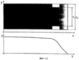
Такой градиент может быть получен различными методами. Один из вариантов заключается в изменении состава материала так, чтобы на горячем конце использовался материал с более высокой теплопроводностью, чем на холодном конце. На желательный градиент температур может повлиять также изменение ширины, как это схематически показано на фиг.11.Such a gradient can be obtained by various methods. One option is to change the composition of the material so that a material with a higher thermal conductivity is used on the hot end than on the cold end. A change in width may also affect the desired temperature gradient, as shown schematically in FIG. 11.
Отбор тока на холодном конце действует как усиленная рекомбинация, и внутренний градиент потенциала в х-направлении повышается, что усиливает амбиполярную диффузию. То есть амбиполярная диффузия носителей заряда еще более усиливается отбором тока, что означает, что отбор тока повышает кпд.Current extraction at the cold end acts as enhanced recombination, and the internal potential gradient in the x-direction increases, which enhances ambipolar diffusion. That is, the ambipolar diffusion of charge carriers is further enhanced by the selection of current, which means that the selection of current increases the efficiency.
Для изобретения имеют принципиальное значение те же физические параметры, что и для традиционной концепции. Впрочем, представленная здесь концепция может повлиять на зависимость между отдельными параметрами, поскольку латеральное изменение параметров оказывает воздействие на кпд всей структуры.For the invention, the same physical parameters are of fundamental importance as for the traditional concept. However, the concept presented here may affect the relationship between the individual parameters, since lateral changes in the parameters affect the efficiency of the entire structure.
В дополнение к этому новая концепция открывает целый ряд новых кандидатов для хороших термоэлектрических материалов.In addition to this, the new concept opens up a whole host of new candidates for good thermoelectric materials.
Едва ли имеются ограничения в выборе материалов, так как все электропроводящие вещества проявляют термоэлектрический эффект /Зеебека/. Впрочем, материалы различаются по кпд, а также по кпд как функции температуры. Таким образом, материалы для применения должны выбираться, исходя из желательного температурного интервала.There are hardly any restrictions in the choice of materials, since all electrically conductive substances exhibit a thermoelectric effect / Seebeck /. However, materials differ in efficiency as well as in efficiency as a function of temperature. Thus, materials for use should be selected based on the desired temperature range.
Сложные полупроводники в связи с их низкой теплопроводностью являются предпочтительными материалами для термоэлементов. В виде примера хороших термоэлектрических материалов можно назвать BigTes, PbTe, SiGe. Также некоторые трех- и четырехкомпонентные соединения показывают хороший кпд. В настоящее время исследование направлено главным образом на поиск этих новых материалов.Complex semiconductors due to their low thermal conductivity are preferred materials for thermocouples. By way of example, good thermoelectric materials include BigTes, PbTe, SiGe. Also, some three- and four-component compounds show good efficiency. Currently, research is mainly aimed at finding these new materials.
Элементарные полупроводники /как Si/ ввиду их слишком хорошей теплопроводности показывают в традиционных конструкциях плохой кпд и поэтому не используются как термоэлектрические материалы.Elementary semiconductors (like Si), due to their too good thermal conductivity, show poor efficiency in traditional designs and therefore are not used as thermoelectric materials.
Однако, благодаря изложенной здесь идее также эти материалы могут иметь высокий кпд, так как в дополнение к соотношению электропроводности и теплопроводности играет роль также распределение температуры.However, thanks to the idea presented here, these materials can also have high efficiency, since in addition to the ratio of electrical conductivity and thermal conductivity, temperature distribution also plays a role.
Необходимы высокие и очень высокие концентрации примесей для поддержания по возможности низкого удельного сопротивления. Величина концентрации примесей, разумеется, зависит от материала. В виде примера, для PbTe необходима концентрация примесей порядка 1018 см-3 и выше.High and very high concentrations of impurities are needed to maintain the lowest possible resistivity. The concentration of impurities, of course, depends on the material. As an example, for PbTe, an impurity concentration of the order of 10 18 cm -3 and higher is required.
Тип контактирования имеет большое значение для новой концепции. Так как внутренние уравнительные токи должны отводиться, то слои должны контактировать селективно. Это селективное контактирование может осуществляться либо прямым и исключительно электрическим присоединением к желательному слою, либо вплавлением контактов.The type of contact is of great importance for the new concept. Since internal equalizing currents must be discharged, the layers must contact selectively. This selective contacting can be carried out either by direct and exclusively electrical connection to the desired layer, or by fusion of the contacts.
Важна не только абсолютная разница температур, но также большую роль играет градиент температур. Умелый выбор распределения температуры при плавном градиенте в зоне высоких температур и при крутом градиенте в конце при низкой температуре позволяет повысить кпд.Not only the absolute temperature difference is important, but also the temperature gradient plays an important role. The skillful choice of temperature distribution with a smooth gradient in the high-temperature zone and with a steep gradient at the end at low temperature allows to increase the efficiency.
Формирующийся внутри градиент потенциалов может быть повышен, например, изменением модуляции потенциала между n- и р-слоем при помощи градиента концентрации примеси. На теплопроводность также можно воздействовать латерально /х-направление/ путем изменения толщин или состава и таким образом получить желательный градиент температур.The potential gradient formed inside can be increased, for example, by changing the modulation of the potential between the n and p layers using an impurity concentration gradient. Thermal conductivity can also be influenced laterally (x-direction) by varying the thickness or composition, and thereby obtain the desired temperature gradient.
Внутренний градиент потенциалов еще больше усиливается за счет отвода носителей заряда. Таким образом устанавливается положительная обратная связь и повышается кпд преобразования энергии.The internal gradient of potentials is further enhanced by the removal of charge carriers. In this way, positive feedback is established and the energy conversion efficiency is increased.
Нужно иметь, по меньшей мере, один р-n-переход. Но могут быть использованы также больше переходов, причем n- и р-слои должны постоянно чередоваться. На фиг.12 представлен пример выполнения с последовательностью слоев р-n-р и двумя р-n-переходами p-n1 и р-n2.You must have at least one pn junction. But more transitions can also be used, with the n and p layers constantly alternating. On Fig presents an example of execution with a sequence of layers pn-p and two pn-junctions pn 1 and pn 2 .
Представленные здесь элементы согласно изобретению могут быть соединены в модули для создания электрической последовательной и термической параллельной схемы. Возможная конструкция такого модуля показана на фиг.13.The elements according to the invention presented here can be connected in modules to create an electrical series and thermal parallel circuit. A possible design of such a module is shown in FIG. 13.
В представленном на фиг.13 примере выполнения три отдельных термоэлемента с последовательностью слоев, как показано на фиг.13 вверху, расположены между двумя пластинами 8 и 9 термически параллельно. Электрически отдельные элементы соединены последовательно, а именно перекрестными проводниками 6'. Пластины 8 и 9 служат для лучшей термической связи и могут по усмотрению также отсутствовать. Предпочтительно они выполнены как хорошие проводники теплоты и для предотвращения электрических коротких замыканий выполняются предпочтительно из керамических материалов, не проводящих электрический ток /например, Аl2O3/.In the embodiment shown in FIG. 13, three separate thermocouples with a sequence of layers, as shown in FIG. 13 at the top, are thermally parallel between the two
Для повышения кпд термоэлемента, состоящего из двух /n- и р-примесных/ слоев 1, 2, и созданного между ними р-n-перехода можно добавить два других слоя 1а, 2а, как показано на фиг.14. К имеющемуся n-слою 1 добавляется высоколегированный n-слой 1а и к р-слою 2 высоколегированный р-слой 2а таким образом, что получается следующая структура из 4 слоев: n+-n-р-р+.To increase the efficiency of the thermoelement consisting of two / n- and p-impurity /
Селективное контактирование остается аналогичным, как и в случае с двумя слоями.Selective contacting remains the same as with two layers.
Существуют прежде всего три области, в которых изобретение может найти применение:There are primarily three areas in which the invention may find application:
1. Термоэлектрические генераторы для прямого преобразования разницы температуры в электрический ток. Благодаря этому назначению возможно получающееся остаточное, которое могло бы остаться неиспользованным, будет использовано.1. Thermoelectric generators for the direct conversion of temperature differences into electric current. Thanks to this designation, the resulting residual, which might have remained unused, will be used.
2. Эффект, обратный генерации. В результате протекания тока один конец будет горячим, а другой холодным. Этот эффект может использоваться для активного охлаждения /для получения низких температур или для отвода теплоты/.2. The effect of reverse generation. As a result of the flow of current, one end will be hot and the other cold. This effect can be used for active cooling / to obtain low temperatures or to remove heat /.
3. Повышенная теплопроводность, которая может использоваться для эффективного пассивного охлаждения, например, в установке кондиционирования воздуха или для /промышленной/ электроники.3. Increased thermal conductivity, which can be used for effective passive cooling, for example, in an air conditioning installation or for / industrial / electronics.
Claims (16)
Applications Claiming Priority (2)
| Application Number | Priority Date | Filing Date | Title |
|---|---|---|---|
| ATA763/2000 | 2000-05-02 | ||
| AT0076300A AT410492B (en) | 2000-05-02 | 2000-05-02 | THERMOELECTRIC ELEMENT WITH AT LEAST ONE N LAYER AND AT LEAST ONE P LAYER |
Publications (2)
| Publication Number | Publication Date |
|---|---|
| RU2002132261A RU2002132261A (en) | 2004-06-10 |
| RU2248647C2 true RU2248647C2 (en) | 2005-03-20 |
Family
ID=3680572
Family Applications (1)
| Application Number | Title | Priority Date | Filing Date |
|---|---|---|---|
| RU2002132261/28A RU2248647C2 (en) | 2000-05-02 | 2001-04-25 | Thermal cell |
Country Status (10)
| Country | Link |
|---|---|
| US (1) | US6762484B2 (en) |
| EP (1) | EP1287566B1 (en) |
| JP (1) | JP3921602B2 (en) |
| KR (1) | KR100581978B1 (en) |
| CN (1) | CN100352073C (en) |
| AT (1) | AT410492B (en) |
| AU (1) | AU2001250149A1 (en) |
| DE (1) | DE50100847D1 (en) |
| RU (1) | RU2248647C2 (en) |
| WO (1) | WO2001084641A1 (en) |
Cited By (3)
| Publication number | Priority date | Publication date | Assignee | Title |
|---|---|---|---|---|
| RU2444814C1 (en) * | 2011-03-29 | 2012-03-10 | Юрий Феликсович Верниковский | Thermoelectric cluster, method of its operation, device to connect active element in it with heat power line, generator (versions) and heat pump (versions) on its basis |
| WO2020197525A1 (en) | 2019-03-26 | 2020-10-01 | Андрей Дмитриевич ХВОРОСТЯНЫЙ | Semiconductor thermoelectric generator |
| RU2781494C2 (en) * | 2018-03-07 | 2022-10-12 | Ргс Дивелопмент Б.В. | Thermoelectric conversion device and its manufacturing method |
Families Citing this family (30)
| Publication number | Priority date | Publication date | Assignee | Title |
|---|---|---|---|---|
| US7038234B2 (en) * | 2001-12-12 | 2006-05-02 | Hi-Z Technology, Inc. | Thermoelectric module with Si/SiGe and B4C/B9C super-lattice legs |
| US6828579B2 (en) * | 2001-12-12 | 2004-12-07 | Hi-Z Technology, Inc. | Thermoelectric device with Si/SiC superlattice N-legs |
| WO2006005126A1 (en) * | 2004-07-12 | 2006-01-19 | Newsouth Innovations Pty Limited | Reversible thermoelectric nanomaterials |
| WO2006033875A2 (en) * | 2004-09-09 | 2006-03-30 | Orobridge, Inc. | Thermoelectric devices with controlled current flow and related methods |
| US20060090787A1 (en) * | 2004-10-28 | 2006-05-04 | Onvural O R | Thermoelectric alternators and thermoelectric climate control devices with controlled current flow for motor vehicles |
| DE102005036407A1 (en) * | 2005-07-29 | 2007-02-01 | Endress + Hauser Wetzer Gmbh + Co. Kg | Evaluation unit for continuous thermocouples |
| US20080017238A1 (en) * | 2006-07-21 | 2008-01-24 | Caterpillar Inc. | Thermoelectric device |
| AT505168B1 (en) | 2007-06-29 | 2008-11-15 | Span Gerhard Dipl Ing Dr | THERMOELECTRIC ELEMENT |
| US8283553B1 (en) | 2007-09-21 | 2012-10-09 | Hrl Laboratories, Llc | Photon enhanced thermoelectric power generation |
| DE102007050741A1 (en) | 2007-10-22 | 2009-04-23 | O-Flexx Technologies Gmbh | Thermoelectric generator |
| DE102008032856A1 (en) | 2008-07-14 | 2010-01-28 | O-Flexx Technologies Gmbh | Heat exchanger for a thermoelectric thin-film element |
| DE102009032906A1 (en) * | 2009-07-10 | 2011-01-20 | O-Flexx Technologies Gmbh | Module with several thermoelectric elements |
| JP5560610B2 (en) * | 2009-08-26 | 2014-07-30 | 富士通株式会社 | Power generation device and power generation system provided with such power generation device |
| DE102009048985A1 (en) | 2009-10-09 | 2011-04-21 | O-Flexx Technologies Gmbh | Module with several thermoelectric elements |
| DE102010005340A1 (en) | 2010-01-21 | 2011-07-28 | O-Flexx Technologies GmbH, 47228 | Method and device for structuring a layer arranged on a substrate |
| KR101701349B1 (en) * | 2010-06-10 | 2017-02-01 | 엘지이노텍 주식회사 | Cooling thermoelectric element and method of manufacturing method of the same |
| EP2591547A1 (en) * | 2010-07-07 | 2013-05-15 | Dynamic Connections, LLC | Renewable energy extraction |
| FR2963165A1 (en) * | 2010-07-22 | 2012-01-27 | St Microelectronics Crolles 2 | METHOD FOR GENERATING ELECTRIC ENERGY IN A SEMICONDUCTOR DEVICE, AND CORRESPONDING DEVICE |
| FR2968134B1 (en) | 2010-11-26 | 2013-05-17 | Schneider Electric Ind Sas | THERMOELECTRIC MODULE WITH IMPROVED YIELD |
| DE102011001653A1 (en) | 2011-03-30 | 2012-10-04 | O-Flexx Technologies Gmbh | Thermoelectric arrangement |
| CN102779936A (en) * | 2011-05-12 | 2012-11-14 | 冯建明 | PN junction tetrode type thermoelectric conversion and refrigeration and heating device |
| RU2477828C1 (en) * | 2011-10-25 | 2013-03-20 | Святослав Михайлович Сергеев | Thermal diode |
| DE102012209619A1 (en) | 2012-06-08 | 2013-12-12 | Robert Bosch Gmbh | Thermoelectric element for converting energy between thermal energy and electrical energy and a method for disassembling the thermoelectric element |
| WO2014114559A1 (en) | 2013-01-24 | 2014-07-31 | O-Flexx Technologies Gmbh | Thermoelectric component, methods for the production thereof, and thermoelectric generator |
| US9627601B2 (en) | 2013-01-24 | 2017-04-18 | O-Flexx Technologies Gmbh | Thermoelectric element and method for the production thereof |
| RU2576414C2 (en) * | 2014-05-21 | 2016-03-10 | Федеральное государственное бюджетное образовательное учреждение высшего профессионального образования "Курганский государственный университет" | Cooling device |
| CN106876569B (en) * | 2015-12-10 | 2019-04-23 | 廖建能 | Electrothermal module |
| WO2018022922A1 (en) * | 2016-07-27 | 2018-02-01 | Novus Energy Technologies, Inc. | Thermoelectric heat pump system |
| JP2020088028A (en) * | 2018-11-19 | 2020-06-04 | トヨタ自動車株式会社 | Thermoelectric conversion element, thermoelectric conversion system, and power generation method using them |
| DE102021209656B3 (en) | 2021-09-02 | 2022-09-29 | Nikolay Iosad | Thermoelectric element, thermoelectric generator and method for their manufacture |
Family Cites Families (24)
| Publication number | Priority date | Publication date | Assignee | Title |
|---|---|---|---|---|
| US2981775A (en) * | 1958-11-12 | 1961-04-25 | Steatite Res Corp | Oxide thermocouple device |
| US3564860A (en) * | 1966-10-13 | 1971-02-23 | Borg Warner | Thermoelectric elements utilizing distributed peltier effect |
| IT1042975B (en) * | 1975-09-30 | 1980-01-30 | Snam Progetti | METHOD FOR THE CONSTRUCTION OF A THERMOELECTRIC MODULE AND MODULE SO OBTAINED |
| JPS571276A (en) * | 1980-06-02 | 1982-01-06 | Tdk Corp | Thermoelectric element and manufacture thereof |
| JPS57169283A (en) * | 1981-04-11 | 1982-10-18 | Tdk Corp | Thermoelectric element |
| JPS59980A (en) * | 1982-06-26 | 1984-01-06 | Tdk Corp | Thermoelectric element |
| DE3315960A1 (en) * | 1983-05-02 | 1984-11-08 | Bschorr, Oskar, Dipl.-Ing. Dr.rer.nat., 8000 München | GENERATION OF VOLTAGE DIFFERENCES |
| FR2598803B1 (en) * | 1986-05-16 | 1988-09-02 | Anvar | DEVICE FOR MEASURING THE INTENSITY OF A RADIATIVE FLOW |
| JPH01208876A (en) * | 1988-02-17 | 1989-08-22 | Matsushita Electric Ind Co Ltd | Thermoelectric device and manufacture thereof |
| EP0369670A3 (en) * | 1988-11-18 | 1992-06-03 | Aspden, Harold Dr. | Thermoelectric energy conversion |
| US5009717A (en) * | 1989-07-18 | 1991-04-23 | Mitsubishi Metal Corporation | Thermoelectric element and method of manufacturing same |
| JPH0463481A (en) * | 1990-03-08 | 1992-02-28 | Mitsubishi Materials Corp | Insulating film coated type thermoelectric generator and manufacture thereof |
| GB2267995B (en) * | 1992-06-17 | 1995-11-08 | Harold Aspden | Thermoelectric heat transfer apparatus |
| JPH0738158A (en) * | 1993-07-16 | 1995-02-07 | Vacuum Metallurgical Co Ltd | Integral sintered silicon germanium thermoelectric conversion device and manufacture thereof |
| US5834828A (en) * | 1993-09-20 | 1998-11-10 | The United States Of America, As Represented By The Secretary Of The Army | Nanoporous semiconductor material and fabrication technique for use as thermoelectric elements |
| GB2283361B (en) * | 1993-10-12 | 1997-04-16 | Harold Aspden | Refrigeration and electrical power generation |
| US5644184A (en) * | 1996-02-15 | 1997-07-01 | Thermodyne, Inc. | Piezo-pyroelectric energy converter and method |
| JP3642885B2 (en) | 1996-06-28 | 2005-04-27 | ジャパンゴアテックス株式会社 | IC chip mounting interposer and IC chip package |
| JPH1022530A (en) * | 1996-07-01 | 1998-01-23 | Sumitomo Special Metals Co Ltd | Thermoplastic conversion element |
| JPH1022531A (en) * | 1996-07-01 | 1998-01-23 | Sumitomo Special Metals Co Ltd | Thermoelectric converter element |
| JPH10144969A (en) * | 1996-11-08 | 1998-05-29 | Sumitomo Special Metals Co Ltd | Thermoelectric conversion element |
| AU6783598A (en) * | 1997-03-31 | 1998-10-22 | Research Triangle Institute | Thin-film thermoelectric device and fabrication method of same |
| JPH11195817A (en) * | 1997-12-27 | 1999-07-21 | Sumitomo Special Metals Co Ltd | Thermoelectric conversion element |
| CN1122319C (en) * | 1997-12-27 | 2003-09-24 | 住友特殊金属株式会社 | Thermoelectric conversion element |
-
2000
- 2000-05-02 AT AT0076300A patent/AT410492B/en not_active IP Right Cessation
-
2001
- 2001-04-25 JP JP2001581354A patent/JP3921602B2/en not_active Expired - Fee Related
- 2001-04-25 CN CNB018089186A patent/CN100352073C/en not_active Expired - Fee Related
- 2001-04-25 DE DE50100847T patent/DE50100847D1/en not_active Expired - Lifetime
- 2001-04-25 RU RU2002132261/28A patent/RU2248647C2/en not_active IP Right Cessation
- 2001-04-25 WO PCT/AT2001/000123 patent/WO2001084641A1/en active IP Right Grant
- 2001-04-25 EP EP01923379A patent/EP1287566B1/en not_active Expired - Lifetime
- 2001-04-25 KR KR1020027014293A patent/KR100581978B1/en not_active IP Right Cessation
- 2001-04-25 AU AU2001250149A patent/AU2001250149A1/en not_active Abandoned
-
2002
- 2002-10-25 US US10/280,065 patent/US6762484B2/en not_active Expired - Lifetime
Non-Patent Citations (1)
| Title |
|---|
| Б.С.Поздняков, Е.А.Котелов. Термоэлектрическая энергетика, М, Атомиздат, 1974, с.29-30. * |
Cited By (4)
| Publication number | Priority date | Publication date | Assignee | Title |
|---|---|---|---|---|
| RU2444814C1 (en) * | 2011-03-29 | 2012-03-10 | Юрий Феликсович Верниковский | Thermoelectric cluster, method of its operation, device to connect active element in it with heat power line, generator (versions) and heat pump (versions) on its basis |
| WO2012134348A1 (en) * | 2011-03-29 | 2012-10-04 | Vernikovsky Yury Felixovich | Thermoelectric cluster, method for operating same, device for connecting an active element in said cluster to a thermoelectric drive, generator (variants) and heat pump (variants) based thereon |
| RU2781494C2 (en) * | 2018-03-07 | 2022-10-12 | Ргс Дивелопмент Б.В. | Thermoelectric conversion device and its manufacturing method |
| WO2020197525A1 (en) | 2019-03-26 | 2020-10-01 | Андрей Дмитриевич ХВОРОСТЯНЫЙ | Semiconductor thermoelectric generator |
Also Published As
| Publication number | Publication date |
|---|---|
| US6762484B2 (en) | 2004-07-13 |
| WO2001084641A1 (en) | 2001-11-08 |
| JP2003533031A (en) | 2003-11-05 |
| EP1287566A1 (en) | 2003-03-05 |
| KR100581978B1 (en) | 2006-05-23 |
| CN100352073C (en) | 2007-11-28 |
| AU2001250149A1 (en) | 2001-11-12 |
| KR20020093070A (en) | 2002-12-12 |
| US20030042497A1 (en) | 2003-03-06 |
| EP1287566B1 (en) | 2003-10-22 |
| ATA7632000A (en) | 2002-09-15 |
| DE50100847D1 (en) | 2003-11-27 |
| JP3921602B2 (en) | 2007-05-30 |
| AT410492B (en) | 2003-05-26 |
| CN1441972A (en) | 2003-09-10 |
Similar Documents
| Publication | Publication Date | Title |
|---|---|---|
| RU2248647C2 (en) | Thermal cell | |
| JP4881919B2 (en) | Thermoelectric generator with thermoelectric element | |
| US9748466B2 (en) | Wafer scale thermoelectric energy harvester | |
| CN100499192C (en) | Low power thermoelectric generator | |
| US9620700B2 (en) | Wafer scale thermoelectric energy harvester | |
| RU2002132261A (en) | THERMOELEMENT | |
| US9620698B2 (en) | Wafer scale thermoelectric energy harvester | |
| US6563227B1 (en) | Temperature control method for integrated circuit | |
| US20040177876A1 (en) | Spatially optimized thermoelectric module | |
| JP2003533031A5 (en) | ||
| KR20050000514A (en) | Thermoelectric device utilizing double-sided peltier junctions and method of making the device | |
| RU2573607C2 (en) | Thermoelectric device | |
| CN101859867A (en) | Thermoelectric element | |
| KR20120064517A (en) | A thermoelectric element and a thermoelectric module | |
| US20040177877A1 (en) | Geometrically optimized thermoelectric module | |
| JP3554861B2 (en) | Thin film thermocouple integrated thermoelectric conversion device | |
| US10763418B2 (en) | Thermoelectric device | |
| CN103794581A (en) | Thermoelectricity radiating device | |
| US20110174351A1 (en) | Module Having A Plurality of Thermoelectric Elements | |
| CN104956505B (en) | Thermoelectric element and its manufacture method | |
| KR20210020461A (en) | Nanowire Thermoelectric device having a 3-Dimensional Stacked Nanowire and Method of Manufacturing the same | |
| KR101701349B1 (en) | Cooling thermoelectric element and method of manufacturing method of the same | |
| US20180226559A1 (en) | Thermoelectric conversion device | |
| LU100175B1 (en) | Thermoelectric device | |
| RU2179354C1 (en) | Semiconductor item |
Legal Events
| Date | Code | Title | Description |
|---|---|---|---|
| MM4A | The patent is invalid due to non-payment of fees |
Effective date: 20170426 |