RU2220450C2 - Biometric transducer and its manufacturing process - Google Patents
Biometric transducer and its manufacturing process Download PDFInfo
- Publication number
- RU2220450C2 RU2220450C2 RU2001104356/09A RU2001104356A RU2220450C2 RU 2220450 C2 RU2220450 C2 RU 2220450C2 RU 2001104356/09 A RU2001104356/09 A RU 2001104356/09A RU 2001104356 A RU2001104356 A RU 2001104356A RU 2220450 C2 RU2220450 C2 RU 2220450C2
- Authority
- RU
- Russia
- Prior art keywords
- chip
- housing
- contact posts
- contact
- coating
- Prior art date
Links
Images

Classifications
-
- A—HUMAN NECESSITIES
- A61—MEDICAL OR VETERINARY SCIENCE; HYGIENE
- A61B—DIAGNOSIS; SURGERY; IDENTIFICATION
- A61B5/00—Measuring for diagnostic purposes; Identification of persons
- A61B5/117—Identification of persons
- A61B5/1171—Identification of persons based on the shapes or appearances of their bodies or parts thereof
- A61B5/1172—Identification of persons based on the shapes or appearances of their bodies or parts thereof using fingerprinting
-
- G—PHYSICS
- G06—COMPUTING; CALCULATING OR COUNTING
- G06F—ELECTRIC DIGITAL DATA PROCESSING
- G06F18/00—Pattern recognition
-
- G—PHYSICS
- G06—COMPUTING; CALCULATING OR COUNTING
- G06V—IMAGE OR VIDEO RECOGNITION OR UNDERSTANDING
- G06V40/00—Recognition of biometric, human-related or animal-related patterns in image or video data
- G06V40/10—Human or animal bodies, e.g. vehicle occupants or pedestrians; Body parts, e.g. hands
- G06V40/12—Fingerprints or palmprints
- G06V40/13—Sensors therefor
- G06V40/1306—Sensors therefor non-optical, e.g. ultrasonic or capacitive sensing
-
- G—PHYSICS
- G07—CHECKING-DEVICES
- G07C—TIME OR ATTENDANCE REGISTERS; REGISTERING OR INDICATING THE WORKING OF MACHINES; GENERATING RANDOM NUMBERS; VOTING OR LOTTERY APPARATUS; ARRANGEMENTS, SYSTEMS OR APPARATUS FOR CHECKING NOT PROVIDED FOR ELSEWHERE
- G07C9/00—Individual registration on entry or exit
- G07C9/30—Individual registration on entry or exit not involving the use of a pass
- G07C9/32—Individual registration on entry or exit not involving the use of a pass in combination with an identity check
- G07C9/37—Individual registration on entry or exit not involving the use of a pass in combination with an identity check using biometric data, e.g. fingerprints, iris scans or voice recognition
-
- Y—GENERAL TAGGING OF NEW TECHNOLOGICAL DEVELOPMENTS; GENERAL TAGGING OF CROSS-SECTIONAL TECHNOLOGIES SPANNING OVER SEVERAL SECTIONS OF THE IPC; TECHNICAL SUBJECTS COVERED BY FORMER USPC CROSS-REFERENCE ART COLLECTIONS [XRACs] AND DIGESTS
- Y10—TECHNICAL SUBJECTS COVERED BY FORMER USPC
- Y10T—TECHNICAL SUBJECTS COVERED BY FORMER US CLASSIFICATION
- Y10T29/00—Metal working
- Y10T29/49—Method of mechanical manufacture
- Y10T29/49002—Electrical device making
- Y10T29/49117—Conductor or circuit manufacturing
- Y10T29/49124—On flat or curved insulated base, e.g., printed circuit, etc.
- Y10T29/4913—Assembling to base an electrical component, e.g., capacitor, etc.
-
- Y—GENERAL TAGGING OF NEW TECHNOLOGICAL DEVELOPMENTS; GENERAL TAGGING OF CROSS-SECTIONAL TECHNOLOGIES SPANNING OVER SEVERAL SECTIONS OF THE IPC; TECHNICAL SUBJECTS COVERED BY FORMER USPC CROSS-REFERENCE ART COLLECTIONS [XRACs] AND DIGESTS
- Y10—TECHNICAL SUBJECTS COVERED BY FORMER USPC
- Y10T—TECHNICAL SUBJECTS COVERED BY FORMER US CLASSIFICATION
- Y10T29/00—Metal working
- Y10T29/49—Method of mechanical manufacture
- Y10T29/49002—Electrical device making
- Y10T29/49117—Conductor or circuit manufacturing
- Y10T29/49169—Assembling electrical component directly to terminal or elongated conductor
- Y10T29/49171—Assembling electrical component directly to terminal or elongated conductor with encapsulating
Abstract
Description
Изобретение относится к биометрическому датчику, содержащему чип и корпус, в который вставлен чип, а также к способу его изготовления. The invention relates to a biometric sensor containing a chip and a housing into which the chip is inserted, as well as to a method for manufacturing it.
Известно, что для идентификации личности регистрируют специфические для данной личности признаки, например папиллярные линии пальцев, т.е. отпечатки пальцев. Подобная идентификация личности может применяться, например, в handys, компьютерах, автомобилях, ключах и т.п. В определенных областях применения, в частности в handys, требуется выполнить корпус чипа как можно меньше с тем, чтобы обеспечить монтаж. В частности, при этом желательна минимальная толщина конструктивного элемента. It is known that, for identification of a person, features specific to a given person are recorded, for example, papillary lines of fingers, i.e. fingerprints. Such identification can be used, for example, in handys, computers, cars, keys, etc. In certain applications, in particular in handys, it is required to make the chip body as small as possible in order to ensure installation. In particular, a minimum thickness of the structural element is desirable.
Из ЕР 0789334 A1 известен биометрический датчик, у которого чип размещен на выводной рамке, причем чип электрически контактирует посредством проволочного монтажа, а посредством заливочной массы заключен таким образом, что чувствительная поверхность датчика доступна через соответствующее отверстие в заливочной массе. Недостатком этого известного датчика является то, что он, с одной стороны, еще относительно велик, а с другой стороны, относительно сложен в изготовлении. A biometric sensor is known from EP 0789334 A1, in which the chip is placed on the lead-out frame, the chip being electrically contacted by wire mounting, and it is enclosed by means of a pouring mass such that the sensitive surface of the sensor is accessible through a corresponding hole in the pouring mass. The disadvantage of this known sensor is that it, on the one hand, is still relatively large, and on the other hand, is relatively difficult to manufacture.
В основе изобретения лежит поэтому задача создания биометрического датчика описанного выше рода, который имел бы как можно меньшую величину и был бы прост в изготовлении. Кроме того, должен быть создан способ как можно более простого изготовления подобного биометрического датчика. The invention is therefore based on the task of creating a biometric sensor of the kind described above, which would be as small as possible and would be simple to manufacture. In addition, a method should be created to make such a biometric sensor as simple as possible.
Эта задача решается согласно изобретению посредством признаков п.1 и п.6 или 9 формулы соответственно. Предпочтительные формы выполнения изобретения описаны в зависимых пунктах формулы. This problem is solved according to the invention by the features of claim 1 and claim 6 or 9, respectively. Preferred embodiments of the invention are described in the dependent claims.
Биометрический датчик согласно изобретению отличается совокупностью следующих признаков:
- чип содержит присоединительные контакты в виде электропроводящих контактных столбиков;
- на верхней стороне чипа находится покрытие для защиты от царапин;
- контактные столбики контактируют с выводами корпуса чипа, предусмотренными в корпусе или на нем;
- между покрытием для защиты от царапин и корпусом чипа, по меньшей мере, вокруг чувствительной поверхности находится адгезионный слой, толщина которого согласована с высотой контактных столбиков с возможностью создания между чипом и корпусом герметичного соединения.The biometric sensor according to the invention is characterized by a combination of the following features:
- the chip contains connecting contacts in the form of conductive contact posts;
- on the upper side of the chip is a coating to protect against scratches;
- contact poles are in contact with the conclusions of the chip housing provided in or on the housing;
- between the coating to protect against scratches and the chip body, at least around the sensitive surface there is an adhesive layer whose thickness is consistent with the height of the contact posts with the possibility of creating a tight connection between the chip and the housing.
Для биометрического датчика согласно изобретению характерно то, что корпус чипа содержит присоединительные контакты для чипа уже в заданных местах. Чип при помещении в корпус находящимися в соответствующих местах контактными столбиками (бугорчатые возвышения из проводящего материала) автоматически соединяют с присоединительными контактами корпуса, так что полностью отпадает необходимость в последующем проволочном монтаже. Чип сидит в корпусе прочно и плотно, так что можно полностью отказаться от заливки, т.е. заключения чипа в синтетическую массу. Далее биометрический датчик согласно изобретению может быть изготовлен очень просто и быстро с низким процентом брака. Особое преимущество при этом состоит в том, что контактирование контактных столбиков с присоединительными контактами корпуса чипа и герметизация между корпусом и чипом происходят посредством адгезионного слоя за одну операцию. Поскольку чип согласно изобретению не приходится заключать с обеих сторон, а отдельный корпус чипа может быть точно согласован с геометрией чипа и последующей областью применения датчика, датчик согласно изобретению может быть изготовлен при заданной чувствительной поверхности также существенно меньшим, чем обычные до сих пор датчики. It is characteristic of the biometric sensor according to the invention that the chip housing contains connecting contacts for the chip already at predetermined locations. When the chip is placed in the housing with contact posts located in appropriate places (tuberous elevations from conductive material), they are automatically connected to the connecting contacts of the housing, so that there is no need for subsequent wire installation. The chip sits firmly and tightly in the housing, so that filling can be completely abandoned, i.e. the conclusion of the chip in the synthetic mass. Further, the biometric sensor according to the invention can be manufactured very simply and quickly with a low reject rate. A particular advantage in this case is that the contacting of the contact columns with the connecting contacts of the chip body and the sealing between the body and the chip occur by means of an adhesive layer in one operation. Since the chip according to the invention does not have to be enclosed on both sides, and the separate housing of the chip can be precisely matched to the geometry of the chip and the subsequent field of application of the sensor, the sensor according to the invention can also be manufactured with a given sensitive surface substantially smaller than conventional sensors.
Согласно предпочтительной форме выполнения дополнительно к находящимся в контакте с выводами контактным столбикам на верхней стороне чипа в месте, препятствующем опрокидыванию чипа относительно корпуса, предусмотрен, по меньшей мере, один опорный столбик, подобный "Dummy-Bump", гарантирует то, что чип после помещения в соответствующее углубление корпуса будет ориентирован копланарно корпусу. Этим гарантировано безупречное контактирование всех контактных столбиков чипа с соответствующими присоединительными контактами выводов корпуса. According to a preferred embodiment, in addition to the contact poles in contact with the terminals on the upper side of the chip, at least one supporting pole, such as a “Dummy-Bump”, is provided to the chip to ensure that the chip after placement into the corresponding recess of the body will be oriented coplanarly to the body. This ensures flawless contacting of all contact columns of the chip with the corresponding connecting contacts of the case leads.
Целесообразно адгезионный слой состоит из рамкообразной огибающей клеевой пленки, размещаемой вокруг чувствительной поверхности чипа. Advantageously, the adhesive layer consists of a frame-shaped envelope of an adhesive film placed around the sensitive surface of the chip.
Согласно предпочтительной форме выполнения корпус чипа выполнен в виде отлитого под давлением корпуса, причем выводы заделаны в материал корпуса и проходят к внешнему краю корпуса. За счет этого можно избежать последующего повреждения выводов. Выступающие на внешнем краю корпуса выводы образуют ножки, которые могут быть выполнены в виде вставных, паяных или зажимных контактов. According to a preferred embodiment, the chip housing is made in the form of a die-cast housing, the leads being embedded in the housing material and extending to the outer edge of the housing. Due to this, you can avoid subsequent damage to the conclusions. The findings protruding on the outer edge of the housing form legs, which can be made in the form of plug-in, soldered or clamping contacts.
Способ согласно изобретению для изготовления биометрического датчика по п.6 формулы отличается совокупностью следующих операций:
а) выполнение проводящих контактных столбиков на присоединительных контактах чипов полупроводниковой пластины;
б) нанесение на лицевую сторону полупроводниковой пластины покрытия для защиты от царапин;
в) удаление покрытия для защиты от царапин с верхней стороны контактных столбиков;
г) отделение чипов;
д) нанесение адгезионного слоя вокруг чувствительной поверхности чипа;
е) помещение чипа в корпус, в котором
ж) предусмотрены электрические выводы, причем
з) склеивание чипа с корпусом и контактирование контактных столбиков с выводами корпуса осуществляют одновременно.The method according to the invention for the manufacture of a biometric sensor according to
a) the implementation of the conductive contact columns on the connecting contacts of the chips of the semiconductor wafer;
b) applying a coating to the front of the semiconductor wafer to protect it from scratches;
c) removing the coating to protect from scratches on the upper side of the contact posts;
d) chip separation;
d) applying an adhesive layer around the sensitive surface of the chip;
f) placing the chip in the housing in which
g) electrical leads are provided, moreover
h) bonding the chip with the housing and contacting the contact posts with the findings of the housing is carried out simultaneously.
Для способа согласно изобретению характерно, таким образом, то, что уже в процессе изготовления полупроводниковой пластины соответствующие контактные столбики, т. е. бугорчатые проводящие возвышения, выполняют на выводах чипа полупроводниковой пластины. Это может происходить, например, посредством трафаретной печати. После этого верхнюю сторону (лицевую сторону) полупроводниковой пластины снабжают преимущественно прозрачным покрытием для защиты от царапин, толщина слоя которого согласована с высотой контактных столбиков. Контактные столбики затем освобождают, преимущественно способом химико-механического полирования (СМР), от покрытия для защиты от царапин и, при необходимости, от имеющегося оксидного слоя. Одновременно за счет этой операции достигают выравнивания контактных столбиков, т.е. производят копланарность между ними, что улучшает возможность контактирования в последующих процессах. После отделения чипов вокруг чувствительной поверхности датчика наносят адгезионное средство, преимущественно клеевую пленку, толщина которой согласована с высотой контактных столбиков. Чип устанавливают в отвечающем требованиям к изделию корпусе, преимущественно в отлитом под давлением из пластмассы корпусе, причем склеивание чипа с корпусом и электрическое контактирование между контактными столбиками и корпусом осуществляют за одну операцию. Thus, it is characteristic of the method according to the invention that already during the manufacturing process of the semiconductor wafer, the corresponding contact posts, i.e., tuberous conductive elevations, are carried out at the chip leads of the semiconductor wafer. This may occur, for example, by screen printing. After that, the upper side (front side) of the semiconductor wafer is provided mainly with a transparent coating for protection against scratches, the layer thickness of which is consistent with the height of the contact posts. The contact posts are then freed, primarily by chemical mechanical polishing (CMP), of the coating to protect it from scratches and, if necessary, from the existing oxide layer. At the same time, alignment of the contact posts, i.e. produce coplanarity between them, which improves the ability to contact in subsequent processes. After the chips are separated, an adhesive agent is applied around the sensitive surface of the sensor, mainly an adhesive film, the thickness of which is consistent with the height of the contact posts. The chip is installed in a housing that meets the requirements of the product, mainly in a die-cast plastic housing, and the chip is glued to the housing and electrical contact between the contact posts and the housing is carried out in one operation.
Способом согласно изобретению осуществляют тем самым выравнивание контактных столбиков для достижения копланарности и удаление защитного слоя, а также оксидного слоя в плоскости полупроводниковой пластины. Контактирование контактных столбиков с корпусом чипа и герметизация между корпусом и чипом происходят за одну операцию. Таким образом, датчик может быть изготовлен очень просто и экономично и с очень малыми размерами. By the method according to the invention, the contact columns are thus aligned to achieve coplanarity and the protective layer as well as the oxide layer are removed in the plane of the semiconductor wafer. Contacting the contact posts with the chip housing and sealing between the housing and the chip occur in one operation. Thus, the sensor can be manufactured very simply and economically and with very small dimensions.
В качестве альтернативы способу, при котором на всю лицевую сторону полупроводниковой пластины наносят покрытие для защиты от царапин и покрытие для защиты от царапин, затем снова удаляют с верхней стороны контактных столбиков, можно также наносить покрытие для защиты от царапин на лицевую сторону полупроводниковой пластины таким образом, что посредством подходящего маскирования в зоне контактных столбиков в покрытии для защиты от царапин освобождаются отверстия, причем маску затем снова удаляют. As an alternative to the method in which the entire front side of the semiconductor wafer is coated with a scratch-resistant coating and the scratch-resistant coating, then removed again from the upper side of the contact posts, the scratch-resistant coating may also be applied to the front of the semiconductor wafer in this way that by suitable masking in the area of the contact posts in the coating to prevent scratches, the holes are freed, and the mask is then removed again.
Изобретение более подробно поясняется ниже на примере с помощью чертежей, на которых изображают: фиг.1 - биометрический датчик согласно изобретению в разобранном виде; фиг.2 - вид датчика из фиг.1 в перспективе, в частичном разрезе; фиг.3 - сечение датчика из фиг.2 по линии А-А из фиг.4; фиг. 4 - вид сверху на датчик из фиг.2; фиг.5 - сечение датчика из фиг.2 в увеличенном виде. The invention is explained in more detail below by way of example with the help of the drawings, in which: FIG. 1 shows a disassembled biometric sensor according to the invention; figure 2 is a view of the sensor of figure 1 in perspective, in partial section; figure 3 is a cross section of the sensor of figure 2 along the line aa of figure 4; FIG. 4 is a plan view of the sensor of FIG. 2; figure 5 is a cross section of the sensor of figure 2 in an enlarged view.
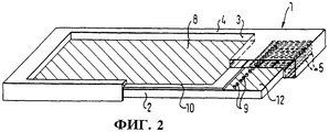
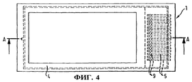
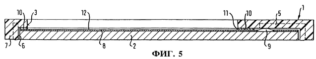
Из фиг. 1-5 виден биометрический датчик, состоящий, в основном, из корпуса 1 и чипа 2. From FIG. Figures 1-5 show a biometric sensor, consisting mainly of housing 1 and chip 2.
Корпус 1 чипа представляет собой прямоугольный при виде сверху, отлитый под давлением из пластмассы корпус. Также прямоугольная сквозная выемка 3 корпуса 1 имеет такую величину, что в нее может быть вставлена передняя часть пальца, на которой находятся папиллярные линии. Далее выемка 3 рассчитана таким образом, что в передней краевой зоне и в обеих боковых краевых зонах имеется только одна узкая перемычка 4. Задняя краевая зона корпуса 1 выполнена шире и содержит множество лежащих рядом выводов 5, уже интегрированных в корпус 1. Эти выводы 5 проходят в изображенном примере выполнения на нижней стороне корпуса 1, однако могут быть также полностью заделаны в материал корпуса, так что для контактирования свободными остаются только их передние и задние концы. The housing 1 of the chip is a rectangular when viewed from above, molded from plastic housing. Also, the rectangular through
С нижней стороны в корпусе 1 выполнено центральное углубление 6, так что образуется выступающий вниз, огибающий узкий край 7, полностью охватывающий с боков вставленный чип 2 датчика. Во вставленном состоянии нижняя сторона чипа 2 находится в одной плоскости с нижней стороной огибающего края 7. Как видно, ширина края 7 также на переднем и заднем торцах корпуса 1 относительно мала, так что общая длина корпуса 1 лишь немного больше общей длины чипа 2. A
Чип 2 содержит прямоугольное чувствительное поле 8, величина которого приблизительно соответствует величине выемки 3 корпуса 1. Во вставленном состоянии чипа 2 чувствительное поле 8 ориентировано относительно выемки 3 корпуса 1, так что для оценки папиллярных линий приложенного пальца может быть использована максимальная площадь чувствительного поля. The chip 2 contains a rectangular
Идущие от чувствительного поля 8 выводы (не показаны) заканчиваются на верхней стороне чипа 2 множеством лежащих в ряд присоединительных контактов, выполненных в виде электропроводящих контактных столбиков 9, т.е. бугорчатых возвышений. Эти контактные столбики 9 могут быть выполнены на полупроводниковой пластине, например, посредством трафаретной печати. Далее контактные столбики 9 расположены таким образом, что во вставленном состоянии чипа 2 каждый контактный столбик 9 вступает в контакт с соответствующим выводом 5 корпуса 1, в результате чего возникает электрическое соединение с выводами 5. The outputs (not shown) coming from the
На верхней стороне чипа 2 находится далее изображенное на фиг.1 и 2 в заштрихованном виде прозрачное покрытие 12 для защиты от царапин, которое наносят на всю поверхность чипа 2 еще при изготовлении полупроводниковой пластины. Толщина этого покрытия 12 для защиты от царапин согласована с высотой контактных столбиков 9. Далее покрытие 12 для защиты от царапин, а также при необходимости имеющийся оксидный слой снова удаляют с верхней стороны контактных столбиков 9, например, посредством способа химико-механического полирования, так что между контактными столбиками 9 и выводами 5 может быть образовано электропроводящее соединение. On the upper side of the chip 2 is further shown in shaded form a
Во избежание опрокидывания чипа 2 внутри корпуса 1 при монтаже в передней концевой зоне чипа 2 могут быть предусмотрены опорные столбики, которые соответствуют контактным столбикам 9, однако выполняют не электропроводящую, а всего лишь поддерживающую функцию. In order to prevent the chip 2 from tipping over inside the housing 1, when mounted in the front end zone of the chip 2, support posts can be provided that correspond to the contact posts 9, however, they do not carry out an electrically conductive, but only supportive function.
На отделенный от полупроводниковой пластины чип 2 или на покрытие 12 для защиты от царапин наносят адгезионный слой 10 в виде рамкообразной клеевой пленки. Центральное свободное пространство 11 адгезионного слоя 10 соответствует величине чувствительного поля 8 или величине выемки 3 корпуса 1. Далее толщина адгезионного слоя 10 согласована с высотой контактных столбиков 9. Адгезионный слой 10 служит для вклеивания чипа 2 в корпус 1. Одновременно за счет адгезионного слоя 10 создается огибающая уплотнительная рамка, которая обеспечивает огибающее герметичное соединение между корпусом 1 и чипом 2. On the chip 2 separated from the semiconductor wafer or on the
Если чип 2 с целью склеивания вставляют в углубление 6 корпуса 1, то одновременно происходят непосредственное электрическое контактирование контактных столбиков 9 с выводами 5 корпуса 1, а также герметизация между чипом 2 и корпусом 1. If the chip 2 is inserted into the
Claims (9)
Applications Claiming Priority (2)
| Application Number | Priority Date | Filing Date | Title |
|---|---|---|---|
| DE19831570.8 | 1998-07-14 | ||
| DE19831570A DE19831570A1 (en) | 1998-07-14 | 1998-07-14 | Biometrical sensor for fingerprint identification for mobile phone |
Publications (2)
| Publication Number | Publication Date |
|---|---|
| RU2001104356A RU2001104356A (en) | 2003-01-20 |
| RU2220450C2 true RU2220450C2 (en) | 2003-12-27 |
Family
ID=7874033
Family Applications (1)
| Application Number | Title | Priority Date | Filing Date |
|---|---|---|---|
| RU2001104356/09A RU2220450C2 (en) | 1998-07-14 | 1999-07-12 | Biometric transducer and its manufacturing process |
Country Status (12)
| Country | Link |
|---|---|
| US (2) | US6528723B2 (en) |
| EP (1) | EP1119823B1 (en) |
| JP (1) | JP3413176B2 (en) |
| KR (1) | KR100400366B1 (en) |
| CN (1) | CN1132120C (en) |
| AT (1) | ATE232322T1 (en) |
| BR (1) | BR9912812A (en) |
| DE (2) | DE19831570A1 (en) |
| ES (1) | ES2192409T3 (en) |
| RU (1) | RU2220450C2 (en) |
| UA (1) | UA57844C2 (en) |
| WO (1) | WO2000004491A1 (en) |
Families Citing this family (20)
| Publication number | Priority date | Publication date | Assignee | Title |
|---|---|---|---|---|
| US8882666B1 (en) | 1998-05-08 | 2014-11-11 | Ideal Life Inc. | Personal health monitoring and/or communication system |
| DE19831570A1 (en) * | 1998-07-14 | 2000-01-20 | Siemens Ag | Biometrical sensor for fingerprint identification for mobile phone |
| DE50008411D1 (en) * | 2000-03-24 | 2004-12-02 | Infineon Technologies Ag | Housing for biometric sensor chips |
| JP2002047840A (en) * | 2000-08-02 | 2002-02-15 | Masahiko Okuno | Switching mechanism with biometrics data authentification device, switching method jointly using biometrics data authentification, and recording medium having switching program jointly using biometrics data authentification recorded therein |
| DE10120362A1 (en) * | 2001-04-26 | 2002-11-21 | Integrated Electronic Systems Sys Consulting Gmbh | Injection molding |
| AU2002310087A1 (en) * | 2001-05-22 | 2002-12-03 | Atrua Technologies, Inc. | Improved connection assembly for integrated circuit sensors |
| US7418255B2 (en) | 2002-02-21 | 2008-08-26 | Bloomberg Finance L.P. | Computer terminals biometrically enabled for network functions and voice communication |
| JP4160851B2 (en) * | 2003-03-31 | 2008-10-08 | 富士通株式会社 | Semiconductor device for fingerprint recognition |
| DE10325863A1 (en) * | 2003-06-06 | 2005-01-05 | Infineon Technologies Ag | A method of manufacturing an integrated fingerprint sensor and sensor circuitry and injection assembly |
| US8034294B1 (en) | 2003-07-15 | 2011-10-11 | Ideal Life, Inc. | Medical monitoring/consumables tracking device |
| US8571880B2 (en) * | 2003-08-07 | 2013-10-29 | Ideal Life, Inc. | Personal health management device, method and system |
| US20060293891A1 (en) * | 2005-06-22 | 2006-12-28 | Jan Pathuel | Biometric control systems and associated methods of use |
| US8358816B2 (en) * | 2005-10-18 | 2013-01-22 | Authentec, Inc. | Thinned finger sensor and associated methods |
| WO2010113712A1 (en) * | 2009-03-31 | 2010-10-07 | アルプス電気株式会社 | Capacitance type humidity sensor and method for manufacturing same |
| DE202009018513U1 (en) | 2009-10-10 | 2011-12-09 | Brose Fahrzeugteile Gmbh & Co. Kommanditgesellschaft, Hallstadt | Device for controlling an adjusting drive of a motor vehicle |
| EP2444415A1 (en) * | 2010-10-20 | 2012-04-25 | Genoplante-Valor | 1-Deoxy-D-xylulose 5-phosphate synthase alleles responsible for enhanced terpene biosynthesis |
| US9089270B2 (en) | 2011-06-29 | 2015-07-28 | Lg Electronics Inc. | Terminal and control method thereof |
| KR101298636B1 (en) | 2013-07-05 | 2013-08-20 | (주)드림텍 | Method of manufacturing fingerprint recognition home key for strengthening adhesion and screening effect between sensing surface and coating layer and the fingerprint recognition home key structure thereof |
| US10014189B2 (en) * | 2015-06-02 | 2018-07-03 | Ngk Spark Plug Co., Ltd. | Ceramic package with brazing material near seal member |
| CN106127195B (en) * | 2016-08-30 | 2017-11-17 | 广东欧珀移动通信有限公司 | Fingerprint module, fingerprint module preparation method and mobile terminal |
Family Cites Families (19)
| Publication number | Priority date | Publication date | Assignee | Title |
|---|---|---|---|---|
| US4429413A (en) * | 1981-07-30 | 1984-01-31 | Siemens Corporation | Fingerprint sensor |
| FR2626408B1 (en) * | 1988-01-22 | 1990-05-11 | Thomson Csf | LOW-SIZE IMAGE SENSOR |
| EP0393206B1 (en) * | 1988-10-14 | 1996-05-08 | Matsushita Electric Industrial Co., Ltd. | Image sensor and method of producing the same |
| DE69006609T2 (en) * | 1989-03-15 | 1994-06-30 | Ngk Insulators Ltd | Ceramic lid for closing a semiconductor element and method for closing a semiconductor element in a ceramic package. |
| US5483100A (en) * | 1992-06-02 | 1996-01-09 | Amkor Electronics, Inc. | Integrated circuit package with via interconnections formed in a substrate |
| JPH06196598A (en) * | 1992-12-25 | 1994-07-15 | Oki Electric Ind Co Ltd | Mounting structure for semiconductor chip |
| JP3550237B2 (en) * | 1994-12-26 | 2004-08-04 | 株式会社東芝 | Personal authentication device |
| KR0148733B1 (en) * | 1995-04-27 | 1998-08-01 | 문정환 | A package for solid state imaging device and fabrication method thereof |
| FR2736179B1 (en) * | 1995-06-27 | 1997-07-25 | Thomson Csf Semiconducteurs | AUTHENTICATION SYSTEM BASED ON FINGERPRINT RECOGNITION |
| DE19527661C2 (en) * | 1995-07-28 | 1998-02-19 | Optrex Europ Gmbh | Carrier comprising electrical conductors with an electronic component and method for contacting conductors of a substrate with contact warts of an electronic component |
| JP4024335B2 (en) * | 1996-01-26 | 2007-12-19 | ハリス コーポレイション | Integrated circuit device having an opening exposing die of integrated circuit and manufacturing method thereof |
| US5956415A (en) * | 1996-01-26 | 1999-09-21 | Harris Corporation | Enhanced security fingerprint sensor package and related methods |
| US5963679A (en) * | 1996-01-26 | 1999-10-05 | Harris Corporation | Electric field fingerprint sensor apparatus and related methods |
| DE19634849A1 (en) * | 1996-08-28 | 1998-03-05 | Siemens Ag | Method and arrangement for identifying people |
| US5887343A (en) * | 1997-05-16 | 1999-03-30 | Harris Corporation | Direct chip attachment method |
| JP2907188B2 (en) * | 1997-05-30 | 1999-06-21 | 日本電気株式会社 | Semiconductor device, method of mounting semiconductor device, and method of manufacturing semiconductor device |
| EP0941696A1 (en) * | 1998-03-03 | 1999-09-15 | Siemens Aktiengesellschaft | Fingertipsensor with integrated bushbutton switch |
| DE19831570A1 (en) * | 1998-07-14 | 2000-01-20 | Siemens Ag | Biometrical sensor for fingerprint identification for mobile phone |
| US6307258B1 (en) * | 1998-12-22 | 2001-10-23 | Silicon Bandwidth, Inc. | Open-cavity semiconductor die package |
-
1998
- 1998-07-14 DE DE19831570A patent/DE19831570A1/en not_active Withdrawn
-
1999
- 1999-07-12 CN CN998086711A patent/CN1132120C/en not_active Expired - Fee Related
- 1999-07-12 ES ES99961981T patent/ES2192409T3/en not_active Expired - Lifetime
- 1999-07-12 WO PCT/DE1999/002146 patent/WO2000004491A1/en active IP Right Grant
- 1999-07-12 KR KR10-2001-7000574A patent/KR100400366B1/en not_active IP Right Cessation
- 1999-07-12 JP JP2000560540A patent/JP3413176B2/en not_active Expired - Fee Related
- 1999-07-12 RU RU2001104356/09A patent/RU2220450C2/en not_active IP Right Cessation
- 1999-07-12 EP EP99961981A patent/EP1119823B1/en not_active Expired - Lifetime
- 1999-07-12 BR BR9912812-8A patent/BR9912812A/en not_active IP Right Cessation
- 1999-07-12 DE DE59904237T patent/DE59904237D1/en not_active Expired - Lifetime
- 1999-07-12 AT AT99961981T patent/ATE232322T1/en not_active IP Right Cessation
- 1999-12-07 UA UA2001010268A patent/UA57844C2/en unknown
-
2001
- 2001-01-16 US US09/761,806 patent/US6528723B2/en not_active Expired - Lifetime
-
2002
- 2002-11-06 US US10/289,087 patent/US6836953B2/en not_active Expired - Fee Related
Also Published As
| Publication number | Publication date |
|---|---|
| BR9912812A (en) | 2001-05-02 |
| CN1309794A (en) | 2001-08-22 |
| JP3413176B2 (en) | 2003-06-03 |
| US6528723B2 (en) | 2003-03-04 |
| UA57844C2 (en) | 2003-07-15 |
| WO2000004491A1 (en) | 2000-01-27 |
| ES2192409T3 (en) | 2003-10-01 |
| US6836953B2 (en) | 2005-01-04 |
| EP1119823A1 (en) | 2001-08-01 |
| ATE232322T1 (en) | 2003-02-15 |
| DE19831570A1 (en) | 2000-01-20 |
| CN1132120C (en) | 2003-12-24 |
| KR20010053523A (en) | 2001-06-25 |
| DE59904237D1 (en) | 2003-03-13 |
| EP1119823B1 (en) | 2003-02-05 |
| US20030062621A1 (en) | 2003-04-03 |
| JP2002520627A (en) | 2002-07-09 |
| KR100400366B1 (en) | 2003-10-04 |
| US20010012201A1 (en) | 2001-08-09 |
Similar Documents
| Publication | Publication Date | Title |
|---|---|---|
| RU2220450C2 (en) | Biometric transducer and its manufacturing process | |
| TWI249712B (en) | Memory card and its manufacturing method | |
| US5031076A (en) | Multifunctional card having a static protection | |
| TW526454B (en) | Casing for biometric sensor-chips | |
| RU2214627C2 (en) | Sensory unit for identifying biometrical attributes, especially fingerprints | |
| RU2001104356A (en) | BIOMETRIC SENSOR AND METHOD FOR ITS MANUFACTURE | |
| TWI325618B (en) | Film type package for fingerprint sensor | |
| JPH022100A (en) | Structure of ic card | |
| US6787388B1 (en) | Surface mount package with integral electro-static charge dissipating ring using lead frame as ESD device | |
| US7220915B1 (en) | Memory card and its manufacturing method | |
| US4934944A (en) | Chip carrier socket with open aperture | |
| KR100922529B1 (en) | Semiconductor device having a built-in contact-type sensor and manufacturing method of such a semiconductor device | |
| US6036173A (en) | Semiconductor element having a carrying device and a lead frame and a semiconductor chip connected thereto | |
| US6969898B1 (en) | Optical semiconductor housing and method for making same | |
| KR100572425B1 (en) | Pc adapter cards and method of manufacturing the same | |
| JP2007213212A (en) | Ic card and its manufacturing method | |
| JP3248853B2 (en) | Structure of sealed semiconductor device having a plurality of IC chips | |
| JP3286196B2 (en) | Structure of sealed semiconductor device having a plurality of IC chips | |
| JPS59116891A (en) | Lsi card | |
| JPS617638A (en) | Semiconductor device | |
| JPH054059Y2 (en) | ||
| JPH0376693A (en) | Ic card | |
| JPH01106448A (en) | Memory cartridge | |
| JPH07115553B2 (en) | IC card manufacturing method | |
| JPH07202077A (en) | Semiconductor device |
Legal Events
| Date | Code | Title | Description |
|---|---|---|---|
| MM4A | The patent is invalid due to non-payment of fees |
Effective date: 20160713 |