RU2017241C1 - Memory - Google Patents
Memory Download PDFInfo
- Publication number
- RU2017241C1 RU2017241C1 SU4943531A RU2017241C1 RU 2017241 C1 RU2017241 C1 RU 2017241C1 SU 4943531 A SU4943531 A SU 4943531A RU 2017241 C1 RU2017241 C1 RU 2017241C1
- Authority
- RU
- Russia
- Prior art keywords
- inputs
- input
- address
- output
- outputs
- Prior art date
Links
Images


Landscapes
- Television Signal Processing For Recording (AREA)
Abstract
Description
Изобретение относится к автоматике и вычислительной технике и может быть использовано при построении быстродействующих ЗУ из блоков памяти, не обладающих достаточным быстродействием, с сохранением функциональных возможностей ЗУ с произвольной выборкой. The invention relates to automation and computer technology and can be used to build high-speed memory from memory units that do not have sufficient speed, while maintaining the functionality of a random access memory.
Известны ОЗУ [1, 2], содержащие накопители, логические компоненты, элементы управления и позволяющие повысить быстродействие (уменьшить цикл обращения) за счет расслоения памяти. Недостатком ОЗУ является невозможность их использования в качестве полноценного ОЗУ с произвольным доступом, быстродействие которого одинаково как в режиме записи, так и в режиме чтения. There are known RAMs [1, 2], which contain drives, logical components, control elements and allow to increase the speed (reduce the cycle of circulation) due to the stratification of memory. The disadvantage of RAM is the inability to use them as a full-fledged random access RAM, the speed of which is the same in both write and read mode.
Наиболее близким по техническим признакам к предлагаемому является ЗУ [3] , содержащее два блока памяти, регистры адреса и числа, счетчик адреса, триггер, коммутаторы. The closest in technical features to the proposed one is the memory [3], containing two memory blocks, address and number registers, address counter, trigger, switches.
Так как цикл записи или считывания определяется работой одного блока памяти, а при считывании адрес определяется счетчиком адреса, то, следоовательно, известному ЗУ свойственны следующие недостатки: невозможность реализации с быстродействием, превосходящим возможности блоков памяти, невозможность считывания по произвольно выбранному адресу и, следовательно, невозможность использования как ЗУ с произвольной выборкой. Since the write or read cycle is determined by the operation of one memory block, and when reading the address is determined by the address counter, therefore, the well-known memory has the following disadvantages: the inability to implement with speed exceeding the capabilities of the memory blocks, the inability to read at an arbitrarily selected address and, therefore, inability to use as a random access memory.
Целью изобретения является повышение быстродействия за счет уменьшения цикла обращения с одновременным обеспечением произвольности доступа к ЗУ. The aim of the invention is to improve performance by reducing the circulation cycle while ensuring random access to the memory.
Сущность изобретения заключается в организации структуры памяти в виде матрицы накопителей, причем запись слова производится параллельно по одному и тому же адресу в два накопителя одной строки матрицы с чередованием во времени по строкам матрицы моментов записи слова при одновременной фиксации в дополнительной одноразрядной памяти признака поступления информации, а считывание производится по тому же адресу параллельно из двух накопителей одного и того же столбца матрицы с чередованием во времени по столбцам моментов выдачи слова при одновременном анализе зафиксированного признака поступления информации для того, чтобы на выход ЗУ выдать информационный код с того накопителя, к которому производилось последнее по времени обращение при записи. При этом одновременно обеспечиваются сокращение в 2 раза цикла обращения по всему ЗУ по сравнению с периодом обращения к каждому из накопителей, входящих в его состав, и возможность записи и чтения по произвольно выбранному адресу. The essence of the invention is to organize the memory structure in the form of a matrix of drives, and the word is recorded in parallel at the same address in two drives of one row of the matrix with alternating in time along the rows of the matrix of moments of recording words while recording in the additional single-bit memory a sign of information and reading is done at the same address in parallel from two drives of the same matrix column with alternating in time along the columns of the moments of the issuance of the word pr and the simultaneous analysis of the recorded sign of the receipt of information in order to output the information code from the storage device to which the recording was last accessed. At the same time, a 2-fold reduction in the circulation cycle for the entire memory is provided as compared with the period of access to each of the drives included in it, and the ability to write and read to an arbitrary address.
Для достижения цели в ЗУ, содержащее накопитель, регистр числа, блок управления и коммутатор, введены три накопителя, четыре фиксатора записи, второй регистр числа, блок приоритета. Информационные входы нечетных и четных накопителей соответственно объединены и соединены с выходами первого и второго регистров, входы которых объединены. Выходы нечетных и четных накопителей соответственно объединены и соединены с первым и вторым информационными входами коммутатора, выход которого является выходом устройства, а управляющие входы соединены с выхоодами блока приоритета, входы которого соединены с информационными выходами фиксаторов записи. Адресные входы последних объединены с адресными входами накопителей. Вторые адресные входы предшествующих фиксаторов записи соединены с адресными выходами последующих фиксаторов записи. Входы синхронизации регистров числа, входы выборки накопителей, первые и вторые входы выборки фиксаторов записи соединены с выходами четырех групп блока управления, выходы разрешения установки, адреса установки, режима, а также выходы пятой группы которого соединены соответственно с одноименными входами, а также информационными входами фиксаторов записи. To achieve the goal, in the memory containing a drive, a number register, a control unit and a switch, three drives, four record latches, a second number register, and a priority block are introduced. The information inputs of the odd and even drives are respectively combined and connected to the outputs of the first and second registers, the inputs of which are combined. The outputs of the odd and even drives are respectively combined and connected to the first and second information inputs of the switch, the output of which is the output of the device, and the control inputs are connected to the outputs of the priority block, the inputs of which are connected to the information outputs of the recording latches. The address inputs of the latter are combined with the address inputs of the drives. The second address inputs of the previous record latches are connected to the address outputs of the subsequent record latches. The inputs of the synchronization of the number registers, the inputs of the sample drives, the first and second inputs of the sample of record latches are connected to the outputs of the four groups of the control unit, the outputs of the installation permit, the installation address, mode, and the outputs of the fifth group of which are connected respectively to the inputs of the same name, as well as information inputs of the latches records.
Каждый из накопителей содержит блок памяти и регистр адреса, выход которого и вход синхронизации соединены соответственно с входом адреса и входом выборки блока памяти, остальные входы и выход которого являются одноименными входами и выходом накопителя. Each drive contains a memory block and an address register, the output of which and the synchronization input are connected respectively to the address input and sample input of the memory block, the remaining inputs and output of which are the inputs and output of the drive of the same name.
Фиксатор записи содержит адресный коммутатор, элемент НЕ, два одноразрядных накопителя, выходы, режимные и информационные входы которых соответственно объединены. Адресный коммутатор имеет четыре направления коммутации. Первые входы по направлениям коммутации с первого по четвертое соединены с входом адреса установки, первым адресным входом, первым и вторым информационными входами фиксатора записи. Вторые входы по направлениям коммутации с первого по четвертое соединены с входом разрешения установки фиксатора записи, с выходом элемента НЕ, с входом режима фиксатора записи. Третьи входы по третьему и четвертому направлениям коммутации соединены с первым и вторым адресными входами фиксатора записи, вход режима которого соединен с входом элемента НЕ и входами режима одноразрядных накопителей, входы выборки которых соединены с первым и вторым входами выборки фиксатора записи. Адресные входы и входы информации одноразрядных накопителей соединены соответственно с выходом адресного коммутатора и с первым информационным входом фиксатора записи, информационным и адресным выходами которого являются соответственно выход одноразрядных накопителей и выход регистра одного из одноразрядных накопителей. The record latch contains an address switch, an element NOT, two one-bit storage devices, outputs, mode and information inputs of which are respectively combined. The address switch has four directions of switching. The first inputs in the directions of switching from the first to the fourth are connected to the input of the installation address, the first address input, the first and second information inputs of the recording latch. The second inputs in the directions of switching from the first to the fourth are connected to the input of the enable setting of the recording latch, with the output of the element NOT, with the input of the recording latch mode. The third inputs in the third and fourth directions of switching are connected to the first and second address inputs of the recording fixture, the mode input of which is connected to the input of the element NOT and the inputs of the single-bit storage mode, the sampling inputs of which are connected to the first and second inputs of the recording fixture sampling. The address inputs and information inputs of single-bit drives are connected respectively to the output of the address switch and to the first information input of the recording latch, the information and address outputs of which are respectively the output of single-bit drives and the register output of one of the single-bit drives.
Блок управления содержит генератор, элемент И-ИЛИ, счетчик выборки, дешифратор, три группы элементов И, счетчик адреса, два элемента ИЛИ, элемент задержки, триггер, одновибратор, формирователь установки, коммутатор запрета, три коммутатора выборки. Выходы групп с первой по пятую блока управления соединены соответственно с выходами элементов И первой группы, коммутаторов выборки с первого по третий, элементов И второй группы. Выходы адреса установки и разрешения установки, а также режима блока управления соединены с выходами младших и старшего разрядов счетчика адреса, а также с выходом первого элемента ИЛИ. Вход режима блока управления соединен с входом управления первого коммутатора выборки, входом запуска одновибратора и через элемент задержки с входом первого элемента ИЛИ. Выход выборки блока управления, выход генератора и первый выход одновибратора соединены с одними входами элемента И-ИЛИ, с другими входами и выходом которого соединены парафазный выход счетчика адреса и счетный вход счетчика выборки. Выходы последнего соединены с входами дешифратора, первыми входами элементов И первой и второй групп, а также с входом второго элемента ИЛИ и счетным входом триггера, парафазный выход которого соединен с первыми входами других элементов И второй группы. Вход установки счетчика выборки соединен с выходом формирователя установки и одноименными входами триггера и счетчика адреса, парафазный выход старшего разряда которого соединен с вторым входом первого и второго элементов ИЛИ, а также с вторыми входами элементов И первой группы и входом разрешения одновибратора. Выходы одновибратора соединены с входами управления коммутатора запрета, входы и выходы которого соединены соответственно с выходами дешифратора и первыми входами элементов И третьей группы. Выходы элементов И первой группы соединены с входами групп первого, второго и третьего коммутаторов выборки, а также с вторыми входами элементов И третьей группы, выходы которых соединены с входами других групп второго и третьего коммутаторов выборки. The control unit contains a generator, an AND-OR element, a sample counter, a descrambler, three groups of AND elements, an address counter, two OR elements, a delay element, a trigger, a one-shot oscillator, a driver, a prohibition switch, and three sample switches. The outputs of the first to fifth control groups are connected respectively to the outputs of the And elements of the first group, the sample switches from the first to the third, the And elements of the second group. The outputs of the installation address and installation permission, as well as the control unit mode, are connected to the outputs of the lower and upper bits of the address counter, as well as to the output of the first OR element. The control unit mode input is connected to the control input of the first sample switch, the one-shot trigger input, and through the delay element with the input of the first OR element. The sample output of the control unit, the output of the generator and the first output of the single-shot are connected to one of the inputs of the AND-OR element, with the other inputs and the output of which are connected the paraphase output of the address counter and the counting input of the sample counter. The outputs of the latter are connected to the inputs of the decoder, the first inputs of the AND elements of the first and second groups, as well as the input of the second OR element and the counting input of the trigger, the paraphase output of which is connected to the first inputs of the other elements of the second group. The installation input of the sample counter is connected to the output of the setup shaper and the inputs of the trigger and address counter of the same name, the high-phase output of which is connected to the second input of the first and second elements of the OR, as well as to the second inputs of the elements of the first group and the resolution input of the one-shot. The outputs of the one-shot are connected to the control inputs of the prohibition switch, the inputs and outputs of which are connected respectively to the outputs of the decoder and the first inputs of the AND elements of the third group. The outputs of the And elements of the first group are connected to the inputs of the groups of the first, second, and third sample switches, as well as to the second inputs of the And elements of the third group, the outputs of which are connected to the inputs of other groups of the second and third switches of the sample.
Блок приоритета содержит элементы НЕ и И-ИЛИ. Входы элементов НЕ и выходы элементов И-ИЛИ являются соответственно входами и выходами блока приоритета. Выходы элементов НЕ соединены с четными входами первого и нечетными входами второго элементов И-ИЛИ, входы элементов НЕ соединены с нечетными входами первого и четными входами второго элементов И-ИЛИ. The priority block contains the elements NOT and AND-OR. The inputs of the elements are NOT and the outputs of the AND-OR elements are respectively the inputs and outputs of the priority block. The outputs of the elements are NOT connected to the even inputs of the first and odd inputs of the second AND-OR elements, the inputs of the elements are NOT connected to the odd inputs of the first and even inputs of the second AND-OR elements.
При исследовании патентной и научно-технической информации не были обнаружены источники, в которых были бы приведены сведения о технических решениях, содержащих совокупность отличительных признаков предлагаемого ЗУ. Хотя известны технические решения, содержащие отдельные отличительные признаки, однако свойства и эффект, которые эти признаки сообщают известным объектом, иные, чем в изобретении, где в соответствии с целью они обеспечивают повышение быстродействия в режимах и записи, и считывания с одновременным сохранением произвольности доступа к памяти. In the study of patent and scientific and technical information, no sources were found that would provide information on technical solutions containing the totality of the distinguishing features of the proposed memory. Although technical solutions are known that contain individual distinctive features, the properties and effect that these features communicate with a known object are different than in the invention, where, in accordance with the purpose, they provide improved performance in both recording and recording modes, while maintaining random access to memory.
На фиг. 1 представлена блок-схема ЗУ; на фиг. 2 - блок-схема блока управления; на фиг. 3 - временная диаграмма работы в режимах записи и считывания. In FIG. 1 is a block diagram of a memory device; in FIG. 2 is a block diagram of a control unit; in FIG. 3 is a timing diagram of operation in the write and read modes.
ЗУ (фиг. 1) содержит накопители 1...4, регистры 5, 6 числа, блок 7 управления, коммутатор 8, фиксаторы 9...12 записи, блок 13 приоритета. The memory (Fig. 1) contains
Вход 14 режима соединен с одноименными входами блока 7 управления и накопителей 1...4. Вход 15 выборки соединен с входом выборки блока 7 управления. Вход 16 адреса соединен с адресными входами накопителей 1...4 и фиксаторов 9. ..12 записи. Информационный вход 17 и выход 18 соединены соответственно с информационными входами регистров 5, 6 числа и выходом коммутатора 8. The
Выхооды групп с первой по пятую (номера групп на фиг. 1, 2 помещены в скобках) блока 7 управления соединены соответственно с входами синхронизации регистров 5, 6 числа, входами выборки накопителей 1...4, первыми, вторыми входами выборки и первыми информационными входами фиксаторов 9, 10, 11, 12, вторые информационные входы которых соединены с первыми информационными входами фиксаторов 11, 12, 9, 10 записи. Выходы разрешения установки, адреса установки, режима блока 7 управления соединены с одноименными входами фиксаторов 9...12 записи, информационные выходы которых соединены с входами блока 13 приоритета. Адресные выходы фиксаторов 9, 10, 11, 12 записи соединены с вторыми адресными входами фиксаторов 12, 9, 10, 11 записи. The outputs of the first to fifth groups (group numbers in Figs. 1, 2 are placed in parentheses) of the
Информационные входы и выходы накопителей 1, 2 и 3, 4 соответственно объединены, входы соединены с выходами регистров 5 и 6 числа, а выходы - с входами коммутатора 8, управляющие входы которого соединены с выходами блока 13 приоритета. The information inputs and outputs of
Каждый из накопителей 1...4 содержит регистр 19 адреса и блок 20 памяти. Информационный вход регистра 19 адреса является входом адреса накопителя (1. . . 4), остальные входы и выход которого соединены с одноименными входами и выходами блока 20 памяти. Выход и синхровход регистра 19 адреса соединены соответственно с адресным входом и входом выборки накопителя (1.. .4). Each of the
Каждый из фиксаторов 9...12 записи состоит из адресного коммутатора 21, элемента НЕ 22, одноразрядных накопителей 23, 24, содержащих регистр 25 адреса и одноразрядный блок 26 памяти. Режимные, адресные, информационные входы и выходы одноразрядных накопителей 23, 24 соответственно объединены. Одноразрядные накопители 23, 24 аналогичны по построению накопителям 1...4. Выходы одноразрядных накопителей 23, 24 и выход регистра 25 адреса являются соответственно информационным и адресным выходом фиксатора (9...12) записи. Входы выборки одноразрядных накопителей 23, 24 являются первым и вторым входами выборки фиксаторов 9...12 записи. Адресные входы одноразрядных накопителей 23, 24 соединены с выходом адресного коммутатора 21, имеющего четыре направления коммутации. Первые входы адресного коммутатора 21 по направлениям 1. ..4 соединены с входом адреса установки, первым входом адреса, первым и вторым информационными входами фиксатора (9...12) записи. Вторые входы адресного коммутатора 21 по направлениям 1...4 соединены с входом разрешения установки, выходом и входом элемента НЕ 22, входом режима фиксатора (9. . .12) записи. Третьи входы коммутатора 21 по направлениям 3, 4 соединены с первым и вторым адресными входами фиксатора (9...12) записи. Вход элемента НЕ 22 соединен с входом режима одноразрядных накопителей 23, 24 и входом режима фиксатора (9...12) записи. Первый вход по направлению 3 коммутации адресного коммутатора 21 соединен с информационными входами одноразрядных накопителей 23, 24. Each of the
Блок 13 приоритета содержит элементы НЕ 27...30 и элементы И-ИЛИ 31, 32. Входы элементов НЕ 27...30 являются входами блока 13 приоритета и соединены с первым, третьим входами элемента И-ИЛИ 31 и вторым, четвертым входами элементы И-ИЛИ 32. Выходы элементов НЕ 27...30 соединены с вторым, четвертым входами элемента И-ИЛИ 31 и первым, третьим входами элементами И-ИЛИ 32. Выходы элементов И-ИЛИ 31, 32 являются выходами блока 13 приоритета. The
Блок 7 управления (фиг. 2) содержит генератор 33 импульсов, элемент И-ИЛИ 34, счетчик 35 выборки, счетчик 36 адреса, группу элементов И 37, элементы ИЛИ 38, 39, элемент 40 задержки, формирователь 41 установки, одновибратор 42, коммутатор 43 запрета, группу элементов И 44, коммутаторы 45, 46, 47 выборки, группу элементов И 48, дешифратор 49, триггер 50. The control unit 7 (Fig. 2) contains a
Выходы групп с первой по пятую блока 7 управления соединены с выходами элементов И 37, коммутаторов 45, 46, 47 выборки, элементов И 48. Выходы адреса установки и разрешения установки, а также режима блока 7 управления соединены соответственно с выходами младших и старшего разрядов счетчика 36 адреса, а также с выходом элемента ИЛИ 38, соединенным с входами управления коммутаторов 46, 47 выборки. Первый (второй) выход элементов И 37 соединен с нечетными (четными) входами первой и нечетной (четной) парой входов второй групп коммутатора 45 выборки, с первыми входами нечетных (четных) элементов И 44, с входами второй группы коммутатора 46 (47) выборки. Выходы элементов И 44 соединены с входами первых групп коммутаторов 46, 47 выборки, а их вторые входы - с выходами коммутатора 43 запрета, входы второй группы которого соединены с выходами дешифратора 49, а нечетная и четная пары входов первой группы соединены соответственно с четной и нечетной парами входов второй группы. Входы управления коммутатора 43 запрета соединены с выходами одновибратора 42, первый выход которого соединен с первым входом элемента И-ИЛИ 34, а вход запуска - с входомо управления коммутатора 45 выборки, входом элемента 40 задержки и входом режима блока 7 управления. Вход разрешения одновибратора 42 соединен с первым и вторым разрешающими входами элемента И-ИЛИ 34, входом элемента ИЛИ 39, входами элементов И 48, выходом старшего разряда счетчика 36 адреса, инверсный выход которого соединен с входом элемента ИЛИ 38 и третьим разрешающим входом элемента И-ИЛИ 34, второй и третий входы которого соединены с входом выборки блока 7 управления и выходом генератора 33. Выход элемента 40 задержки соединен с входом элемента ИЛИ 38. Выход элемента И-ИЛИ 34 соединен со счетным входом счетчика 35 выборки и входами элементов И 37. Выход формирователя 41 установки соединен с установочными входами счетчиков выборки 35 и адреса 36, а также триггера 50. Прямой и инверсный выходы первого разряда счетчика 35 выборки соединены с вторыми входами элементов И 37, а также с первым входом дешифратора 49 и счетным входом триггера 50, прямой и инверсный выходы которого соединены с вторыми входами нечетных элементов И 48. Вторые входы четных элементов И 48 соединены с прямым и инверсным выходами второго разряда счетчика 35 выборки, а также с вторыми входами дешифратора 49 и элемента ИЛИ 39, выход которого соединен со счетным входом счетчика 36 адреса. The outputs of the first to fifth groups of the
Работает ЗУ следующим образом. The memory works as follows.
При включении питания производится обнуление одноразрядных накопителей 23, 24 фиксаторов 9...12 записи. По перепаду на шине питания формирователь 41 установки устанавливает в исходное состояние счетчик 35 выборки, счетчик 36 адреса, триггер 50. Уровень "0" на выходе старшего разряда счетчика 36 адреса удерживает выходы элементов И 48 в состоянии логического "0", поступающего на информационные входы одноразрядных накопителей 23, 24, а также обеспечивает прохождение импульсов генератора 33 через элемент И-ИЛИ 34 на счетчик 35 выборки и прохождение сигналов через элемент ИЛИ 39 на счетчик 36 адреса. Последний осуществляет перебор адресов на входах адреса установки фиксаторов 9...12 записи. Коды адреса поступают через адресные коммутаторы 21 этих фиксаторов на адресные входы одноразрядных накопителей 23, 24 по сигналу разрешения установки с выхода старшего разряда счетчика 36 адреса. Остальные направления адресных коммутаторов 21 запрещены уровнем "0" с выхода элементов И 48 и с выхода элементов НЕ 22. Одноразрядные накопители 23, 24 находятся в режиме записи благодаря сигналу, поступающему на их вход режима с выхода элемента ИЛИ 38. Одновременно на их входы выборки поступают сигналы с выходов коммутаторов 46, 47. Эти сигналы вырабатываются элементами И 37 с помощью счетчика 35 выборки и проходят на входы первых групп коммутаторов 46, 47 выборки через элементы И 44, открытые благодаря высокому уровню на выходах коммутатора 43 запрета, установленному из-за отсутствия сигнала с выходов одновибратора 42. Таким образом производится запись "0" во все одноразрядные накопители 23, 24. When the power is turned on, the single-bit drives 23, 24 of the
По окончании перебора адресов устанавливается в "1" старший разряд счетчика 36 адреса, сигнал с парафазного выхода которого запрещает работу счетчиков выборки 35 и адреса 36 от генератора 33 и разрешает формирование сигналов режима на выходе элемента ИЛИ 38, работу одновибратора 42, формирование информационных сигналов на выходах элементов И 48, прохождение сигналов выборки с входа 15 и сигнала с первого выхода одновибратора 42 через элемент И-ИЛИ 34. Устройство готово к работе. At the end of the address enumeration, the highest digit of the address counter 36 is set to “1”, the signal from the paraphase output of which prohibits the operation of the sample counters 35 and the address 36 from the
В режиме записи производится занесение поступающей информации попеременно в накопители 1, 3 и 2, 4, благодаря чему сокращается цикл записи, так как импульсы выборки на входе 15 могут следовать с частотой, в 2 раза превышающей доопустимую частоту выборки каждого из накопителей. Одновременно с этим осуществляется попеременная запись в одноразрядные накопители 23, 24 нечетных (9, 11) и четных (10, 12) фиксаторов записи. При этом по текущему адресу в одноразрядные накопители 23, 24 одних фиксаторов записи записывается "1" и одновременно по предшествующему адресу (адресу информации, записанной в накопители 1, 3 или 2, 4 в предшествующем такте) в одноразрядные накопители 23, 24 других фиксаторов записи заносится "0". Благодаря этому в фиксаторах 9. . .12 записи фиксируется (но с опозданием на такт) месторасположение "свежей" информации в виде "1" и "устаревшей" в виде "0", записанных в накопителях 23, 24. In the recording mode, the incoming information is recorded alternately in
Для осуществления записи на вход 14 режима (фиг. 3, момент Т1) подают высокий потенциал, на выходы 17 и 16 - соответственно информационный и адресный коды. На вход 15 поступают импульсы выборки с периодом, меньшим времени записи накопителей 1...4 (но не более чем в 2 раза). На первом выходе счетчика 35 выборки частота этих импульсов уменьшается вдвое, и с выходов элементов И 37, где они стробируются сигналами выборки, импульсы попеременно поступают на входы синхронизации регистров 5 и 6 числа, а через входы первой группы коммутатора 45 выборки на входы выборки накопителей 1, 3 и 2, 4. Производится запись информационного кода в регистры 5 и 6 числа и адресного кода в регистры 19 адреса накопителей 1...4. To record on mode input 14 (Fig. 3, moment T1), a high potential is supplied, and outputs and address codes, respectively, are
В связи с тем, что импульсы выборки должны поступать одновременно на два фиксатора записи (9 и 11, 10 и 12), причем в одноразрядные накопители 23, 24 одного из фиксаторов записывается "0", необходимо в начале цикла записи исключить запись "0" в фиксатор записи, не соответствующий тому из накопителей 1. ..4, в котором происходит запоминание входной информации. При отсутствии подобного запрета записываемый в одноразрядные накопители 23, 24 "0" может исказить признак "свежей" информации ("1"), хранившийся в них с предшествовавшего цикла записи. Поэтому по перепаду на входе 14 режима одновибратор 42 формирует на своем втором выходе импульс (вых. 42.2 на фиг. 3), разрешающий прохождение унитарного кода через коммутатор 43 запрета с выхода дешифратора 39. Этот код определяет номер того из фиксаторов 9...12, в одноразрядные накопители 23, 24 которого не следует записывать "0", и блокирует с помощью элементов И 44 прохождение импульса выборки на соответствующие выходы коммутаторов 46, 47 выборки (момент блокирования импульса выборки отмечен на фиг. 3 знаком *). Due to the fact that the sampling pulses must be delivered simultaneously to two recording latches (9 and 11, 10 and 12), moreover, in the one-bit drives 23, 24 of one of the latches being recorded “0”, it is necessary to exclude the record “0” at the beginning of the recording cycle to the recording latch, which does not correspond to that of the
По импульсам выборки, поступающим с выходов коммутатора 45 выборки, производится запись одинакового кода в накопители 1 и 3 или 2 и 4 (т.е. запись по "горизонтали"), причем времени между двумя последовательными импульсами выборки, поступающими на накопители 1...4, достаточно для осуществления записи. Using the sampling pulses coming from the outputs of the
В связи с тем, что в накопителях 1, 3 и 2, 4 по одним и тем же адресам может быть записана разная информация: "свежая" и "устаревшая", в фиксаторах 9...12 записи, соответствующих накопителям 1...4, запоминаются признаки "свежей" и "устаревшей" информации в виде записи "1" и "0", формируемых на выходах элементов И 48 с помощью сигналов с выходов счетчика 35 выборки и триггера 50. Поэтому одновременно с записью информации в накопители 1, 3 производится запись "1" по текущему адресу в одноразрядные накопители 23, 24 фиксатора 9 записи и запись "0" в накопители 23, 24 фиксатора 11 записи по предшествующему адресу, зафиксированному в предыдущем такте в регистре 25 адреса одноразрядного накопителя 23 фиксатора 12 записи (момент Т5, фиг. 3). Текущий адрес поступает с входа 16 в регистры 25 адреса накопителей 23, 24 фиксатора 9 записи по третьему направлению коммутации адресного коммутатора 21, которое открыто сигналом режима с выхода элемента ИЛИ 38 и уровнем "1" с первого выхода группы блока 7 управления (вых. 50 (48.1), фиг. 3). Предшествующий адрес поступает из фиксатора 12 записи в регистры 25 адреса накопителей 23, 24 фиксатора 11 записи по четвертому направлению коммутации адресного коммутатора 21, которое открыто теми же сигналами. Таким образом, в одноразрядных накопителях 23, 24 фиксатора 9 записи запоминается (в виде "1") признак того, что в накопителях 1, 3 по текущему адресу записана "свежая" информация, а в одноразрядных накопителях 23, 24 фиксатора 11 записи запоминается (в виде "0") признак того, что информация, записанная в накопителе 4 по предшествующему адресу, "устарела". Due to the fact that in the
По последующему импульсу выборки (момент Т3, фиг. 3), поступающему на накопители 1, 3 (т.е. через один импульс входной последовательности), текущий адрес с входа 16 проходит через адресный коммутатор 21 фиксатора 11 записи, а предшествующий адрес с адресного выхода фиксатора 10 записи - через адресный коммутатор 21 фиксатора 9 записи. Одноразрядные накопители 23, 24 фиксатора 11 записи хранят "1", а одноразрядные накопители 23, 24 фиксатора 9 записи хранят "0", свидетельствующий о том, что информация, записанная в накопителе 2 по предшествующему адресу, "устарела". According to the subsequent sampling pulse (moment T3, Fig. 3) supplied to
Аналогично происходит запись "1" и "0" по текущему и предшествующему адресам в одноразрядные накопители 23, 24 фиксаторов 10, 12 записи (моменты Т2, Т4, фиг. 3). Similarly, there is a record of "1" and "0" at the current and previous addresses in the single-bit drives 23, 24 of the recording latches 10, 12 (moments T2, T4, Fig. 3).
Сигналы выборки, по которым производится запись в накопители 23, 24 фиксаторов 9. ..12, формируются на выходах коммутаторов 46, 47 выборки (вых. 46.1...46.4, 47.1...47.4 на фиг. 3, моменты записи "1" и "0" показаны стрелками). The sampling signals, which are recorded in the
Таким образом, для полного соответствия информации, записываемой в накопители 1. ..4, и признаков "свежей" и "устаревшей" информации, записываемых в одноразрядные накопители 23, 24, необходимо иметь по окончании цикла записи дополнительный импульс выборки для фиксации "0" по предшествующему адресу и продлить цикл записи для фиксаторов записи на один такт. При этом, естественно, запись информации в накопители 1...4 и занесение "1" по текущему адресу в соответствующие фиксаторы 9...12 записи производиться не должна. Thus, for the complete correspondence of the information recorded in the
При переключении сигнала режима на входе 14 одновибратор 42 (фиг. 3, момент Т6, вых. 42.1) вырабатывает сигнал, имитирующий импульс выборки, поступающий на вход управления коммутатора 43 запрета и через элемент И-ИЛИ 34 на счетный вход счетчика 35 выборки. Задний фронт сигнала режима задерживается элементом 40 задержки, обеспечивая продление цикла записи для фиксаторов записи. When the mode signal is switched at
Состояние выходов счетчика 35 выборки, определяющее номер накопителя и фиксатора записи, в которые заносится информация и "1" по текущему адресу, дешифруется дешифратором 49 и с помощью коммутатора 43 запрета, на выход которого передаются уровни с входов его первой группы, вырабатывается сигнал, блокирующий обращение к соответствующему фиксатору записи (например, к фиксатору 10 записи, как показано на фиг. 3 знаком *, два знака * соответствуют блокировке выборки двух одноразрядных накопителей 23 и 24). На выходах элементов И 48 (вых. 48.2 и вых. 48.4, момент Т6, фиг. 3) с помощью сигналов с выходов счетчика 35 выборки и триггера 50 формируются уровни "1" и "0", соответствующие признакам "свежей" и "устаревшей" информации. Однако "1" не записывается из-за отсутствия сигнала выборки, а "0" записывается в накопители 23, 24 фиксатора 12 записи. Информационный код в накопители 2, 4 не записывается из-за снятия режима записи. На этом цикл записи заканчивается. The status of the outputs of the
В режиме считывания (фиг. 3, Т7...Т10) на вход 15 выборки подают импульсную последовательность с частотой, превышающей допустимую частоту работы накопителей 1...4 (но не более чем в 2 раза). Импульсы выборки формируются на выходах элементов И 37 и через входы второй группы коммутатора 45 выборки поступают на входы выборки накопителей 1, 2 и 3, 4. Адресный код с шины 16 заносится в регистры 19 адреса накопителей 1, 2 и 3, 4 попеременно. Информационный код считывается одновременно с накопителей 1 и 2 или 3 и 4 (считывание по "вертикали") и поступает на информационные входы коммутатора 8, на управляющие входы которого поступают сигналы с блока 13 приоритета, определяющего в каком из накопителей (1...4) содержится "свежая" информация, т.е. поступившая при записи позже. In the reading mode (Fig. 3, T7 ... T10), a pulse sequence with a frequency exceeding the permissible operating frequency of the
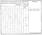
Одновременно с попеременным считыванием информации из накопителей 1, 2 и 3, 4 производится попеременное считывание признаков "свежей" ("1") или "устаревшей" ("0") информации соответственно из всех одноразрядных накопителей 23 или всех накопителей 24 фиксаторов 9...12 записи. Режим считывания фиксаторов записи определяется сигналом режима с выхода элемента ИЛИ 38. Импульсы выборки поступают через входы вторых групп коммутаторов 46, 47 выборки на одноразрядные накопители попеременно, что обеспечивает синхронность считывания с накопителями 1, 2 или 3, 4. Код адреса записывается в регистры 25 адреса, проходя через адресные коммутаторы 21 по второму направлению коммутации, разрешенному сигналом режима с выхода элементов НЕ 22. Возможные (после режима записи) состояния ячеек одноразрядных накопителей 23 или 24 фиксаторов записи 9...12 для текущего момента считывания приведены в таблице. Simultaneously with the alternate reading of information from
Считываемая с одноразрядных накопителей 23 или 24 информация (в виде четырехразрядного кода) поступает в блок 13 приоритета с выхода фиксаторов 9. ..12 записи. Уровни сигналов на выходах блока 13 приоритета определяются следующим. Information read out from single-bit drives 23 or 24 (in the form of a four-bit code) is sent to priority block 13 from the output of
В связи с тем, что при записи занесение "1" в текущем такте в одноразрядные накопители 23, 24 i-го (i=9, 10, 11, 12) фиксатора записи вызывает (благодаря связи адресный выход фиксатора - второй адресный вход) занесение "0" в следующем такте в одноразрядные накопители 23, 24 (i-1)-го фиксатора записи (i-1=12, 9, 10, 11) по тому же адресу, то в комбинациях выходных состояний фиксаторов записи, имеющих только две рядом расположенные "1" (0011, 0110, 1001, 1100) приоритет отдается фиксатору записи, имеющему меньший номер (т. е. 9<10, 10<11, 11<12, по 12<9) и указанной выше группе комбинаций соответствуют номера фиксаторов 11, 10, 12, 9. Именно эти фиксаторы при принятой системе связей между фиксаторами 9...12 записи соответствуют накопителям со "свежей", т.е. позже запомненной, информацией, а именно накопителям с номерами 3, 2, 4, 1, т.е. например, комбинация 0011 свидетельствует о том, что более поздняя информация поступила в накопитель 3, а не в накопитель 4 (если бы было наоборот, то комбинация была бы 00![]()
![]()
Группе комбинаций выходных состояний 0111, 1011, 1101, 1110 соответствуют номера фиксаторов 10, 11, 12, 9 записи, т.е. приоритет отдается накопителям 2, 3, 4, 1. Так, например, комбинация 1101 свидетельствует о том, что более поздняя информация поступила в накопитель 4 (если бы более поздней была информация в накопителе 1 или 2, то комбинация выглядела бы как 110![]()
![]()
![]()
![]()
Группе комбинаций выходных состояний 0001, 0010, 0100, 1000 соответствуют номера фиксаторов 12, 11, 10, 9 записи, т.е. приоритет отдается накопителям 4, 3, 2, 1. Кодовый набор на выходах блока 13 приоритета будет 01, 10, 01, 10. The group of combinations of output states 0001, 0010, 0100, 1000 corresponds to the numbers of the
Группе комбинаций 0101, 1010 соответствуют номера фиксаторов 12 и 10, 11 и 9 записи, т.е. приоритет отдается накопителям 4 и 2, 3 и 1, но так как в этих парах запомнена одинаковая информация, то кодовый набор на выходах блока 13 приоритета должен быть 01, 10. The combination group 0101, 1010 corresponds to the numbers of the
Кодовая комбинация 0000 свидетельствует об отсутствии обращений в данную ячейку накопителей 1...4 и одноразрядных накопителей 23, 24 фиксаторов 9... 12 записи. Code combination 0000 indicates the absence of access to this cell drives 1 ... 4 and single-bit drives 23, 24
Кодовая комбинация 1111 невозможна, так как запись "1" в текущем такте вызывает запись "0" в последующем такте. Code combination 1111 is not possible because recording “1” in the current measure causes recording “0” in the subsequent measure.
В последних двух случаях целесообразно на выходах блока 13 приоритета устанавливать комбинацию 00, которая минимизирует его логическую структуру и запрещает выдачу информации коммутатора 8. Вышеприведенные рассуждения сведены в таблицу (графы 5...8), на основании которой как таблицы истинности построен блок 13 приоритета. In the last two cases, it is advisable to set the combination 00 at the outputs of
Claims (5)
Priority Applications (1)
| Application Number | Priority Date | Filing Date | Title |
|---|---|---|---|
| SU4943531 RU2017241C1 (en) | 1991-06-10 | 1991-06-10 | Memory |
Applications Claiming Priority (1)
| Application Number | Priority Date | Filing Date | Title |
|---|---|---|---|
| SU4943531 RU2017241C1 (en) | 1991-06-10 | 1991-06-10 | Memory |
Publications (1)
| Publication Number | Publication Date |
|---|---|
| RU2017241C1 true RU2017241C1 (en) | 1994-07-30 |
Family
ID=21578305
Family Applications (1)
| Application Number | Title | Priority Date | Filing Date |
|---|---|---|---|
| SU4943531 RU2017241C1 (en) | 1991-06-10 | 1991-06-10 | Memory |
Country Status (1)
| Country | Link |
|---|---|
| RU (1) | RU2017241C1 (en) |
-
1991
- 1991-06-10 RU SU4943531 patent/RU2017241C1/en active
Non-Patent Citations (3)
| Title |
|---|
| 1. Авторское свидетельство СССР N 1180975, кл. G 11C 11/00, 1985. * |
| 2. Авторское свидетельство СССР N 1467572, кл. G 11C 11/00, 1989. * |
| 3. Авторское свидетельство СССР N 1529287, кл. G 11C 11/00, 1987. * |
Similar Documents
| Publication | Publication Date | Title |
|---|---|---|
| EP0242599A2 (en) | Method and apparatus for simulating memory arrays in a logic simulation machine | |
| ATE216529T1 (en) | A SYNCHRONOUS NAND-DRAM MEMORY ARCHITECTURE | |
| RU2017241C1 (en) | Memory | |
| US4549283A (en) | Digital time delay circuit with high speed and large delay capacity | |
| JPH0256048A (en) | Data transfer method and data buffer device | |
| JPH05113929A (en) | Microcomputer | |
| SU1410053A1 (en) | Device for asynchronous associative loading of multiprocessor computing system | |
| SU1322256A1 (en) | Device for sorting information | |
| RU1789993C (en) | Device for editing table elements | |
| SU1290327A1 (en) | Device for generating interruption signal | |
| RU1803909C (en) | Device for arranging in sequence number files | |
| SU769621A1 (en) | Buffer storage | |
| JPS59178667A (en) | Memory device | |
| SU1177856A1 (en) | Storage | |
| SU1287172A1 (en) | Device for generating message route in uniform computer system | |
| SU1325514A1 (en) | Information interval device | |
| SU1606972A1 (en) | Device for sorting data | |
| SU1711229A1 (en) | Storage device | |
| SU1495788A1 (en) | Random number generator | |
| SU1589288A1 (en) | Device for executing logic operations | |
| RU1771533C (en) | Device for digital recording and playback of speech | |
| SU1667150A1 (en) | Indicator device | |
| SU1536366A1 (en) | Device for information input/output device | |
| SU1441384A1 (en) | Device for sorting numbers | |
| SU1689956A1 (en) | Memory addressing device |