KR970000552B1 - 기판의 표면 접촉부를 갖고 있는 딥 트렌치 분리 구조물 및 이의 제조 방법 - Google Patents
기판의 표면 접촉부를 갖고 있는 딥 트렌치 분리 구조물 및 이의 제조 방법 Download PDFInfo
- Publication number
- KR970000552B1 KR970000552B1 KR1019870014760A KR870014760A KR970000552B1 KR 970000552 B1 KR970000552 B1 KR 970000552B1 KR 1019870014760 A KR1019870014760 A KR 1019870014760A KR 870014760 A KR870014760 A KR 870014760A KR 970000552 B1 KR970000552 B1 KR 970000552B1
- Authority
- KR
- South Korea
- Prior art keywords
- trench
- semiconductor
- layer
- substrate
- forming
- Prior art date
- Legal status (The legal status is an assumption and is not a legal conclusion. Google has not performed a legal analysis and makes no representation as to the accuracy of the status listed.)
- Expired - Fee Related
Links
Images


Classifications
-
- H—ELECTRICITY
- H10—SEMICONDUCTOR DEVICES; ELECTRIC SOLID-STATE DEVICES NOT OTHERWISE PROVIDED FOR
- H10W—GENERIC PACKAGES, INTERCONNECTIONS, CONNECTORS OR OTHER CONSTRUCTIONAL DETAILS OF DEVICES COVERED BY CLASS H10
- H10W20/00—Interconnections in chips, wafers or substrates
- H10W20/01—Manufacture or treatment
- H10W20/021—Manufacture or treatment of interconnections within wafers or substrates
-
- H—ELECTRICITY
- H10—SEMICONDUCTOR DEVICES; ELECTRIC SOLID-STATE DEVICES NOT OTHERWISE PROVIDED FOR
- H10W—GENERIC PACKAGES, INTERCONNECTIONS, CONNECTORS OR OTHER CONSTRUCTIONAL DETAILS OF DEVICES COVERED BY CLASS H10
- H10W10/00—Isolation regions in semiconductor bodies between components of integrated devices
- H10W10/01—Manufacture or treatment
- H10W10/041—Manufacture or treatment of isolation regions comprising polycrystalline semiconductor materials
-
- H—ELECTRICITY
- H10—SEMICONDUCTOR DEVICES; ELECTRIC SOLID-STATE DEVICES NOT OTHERWISE PROVIDED FOR
- H10W—GENERIC PACKAGES, INTERCONNECTIONS, CONNECTORS OR OTHER CONSTRUCTIONAL DETAILS OF DEVICES COVERED BY CLASS H10
- H10W10/00—Isolation regions in semiconductor bodies between components of integrated devices
- H10W10/40—Isolation regions comprising polycrystalline semiconductor materials
Landscapes
- Element Separation (AREA)
- Semiconductor Integrated Circuits (AREA)
Abstract
Description
Claims (21)
- 기판 상의 제1도전형 반도체 재료에서 회로들을 절연시키는 방법에 있어서, 상기 반도체 재료를 통하여 상기 기판까지 연장되는 트렌치를 상기 반도체 재료 내에 형성하는 단계, 상기 트렌치의 외부 모서리 주위에 산화 장벽을 형성하되, 상기 장벽이 하부 반도체 재료의 열 산화로 인한 팽창으로부터 상기 외부 모서리를 보호하도록 상기 트렌치 내에 측방향 외향 및 수직으로 연장되도록 하는 단계, 상기 트렌치를 도전성 물질로 채워서 상기 도전성 물질이 상기 트렌치의 밑바닥에서 상기 기판과 전기적으로 접촉되도록 하는 단계, 및 상기 트렌치의 상부에 상기 도전성 물질로의 접속부를 형성하는 단계를 포함하는 것을 특징으로 하는 방법.
- 제1항에 있어서, 질화물층으로 상기 트렌치의 상기 외부 모서리를 코팅함으로써 상기 산화 장벽을 형성하는 단계를 더 포함하는 것을 특징으로 하는 방법.
- 제2항에 있어서, 상기 질화물층과 상기 반도체 재료 사이에 얇은 이산화실리콘층을 형성하는 단계를 더 포함하는 것을 특징으로 하는 방법.
- 제1항에 있어서, 높은 도전성의 다결정성 실리콘으로 상기 트렌치를 채우는 단계를 더 포함하는 것을 특징으로 하는 방법.
- 제1항에 있어서, 상기 트렌치의 상부에 인접하여 제2도전형의 제2반도체 영역을 형성하여, 상기 접속부가 상기 제2반도체 영역을 적어도 부분적으로 덮도록 하는 단계를 더 포함하는 것을 특징으로 하는 방법.
- 제1항의 방법에 따라 제조된 반도체 구조물.
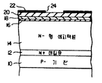
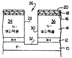
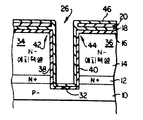
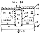
- 베이스를 형성하는 기판을 갖고 있는 집적 회로 내에 상부 표면 접속부를 갖고 있는 트렌치 분리부를 제조하는 방법에 있어서, 상기 기판과 반대의 도전형으로 된 반도체 재료의 에피택셜층을 형성하는 단계, 외부 모서리를 갖는 트렌치를 상기 반도체 재료를 통하여 상기 기판 까지 형성하는 단계, 상기 트렌치의 측벽 상에 전기 절연부를 형성하되, 상기 트렌치의 저부에는 상기 전기 절연부가 없도록 유지하면서 형성하는 단계, 상기 트렌치를 도전성 물질로 채워서, 상기 도전성 물질이 상기 트렌치의 저부에서 상기 기판과 전기적으로 접촉되도록 하는 단계, 및 상기 에피택셜층의 외부에 상기 트렌치의 상부에 배치된 상기 도전성 물질로의 접속부를 형성하는 단계를 포함하는 것을 특징으로 하는 방법.
- 제7항에 있어서, 상기 절연부는 상기 트렌치의 측벽 표면을 산회시킴으로써 형성되는 것을 특징으로 하는 방법.
- 제8항에 있어서, 적어도 상기 트렌치의 외부 모서리에서는, 산화 처리된 트렌치 측벽 위에 산화 장벽을 형성하는 단계를 더 포함하는 것을 특징으로 하는 방법.
- 제7항에 있어서, 인-시추(in situ) 도핑된 다결정성 실리콘으로 상기 트렌치를 채우는 단계를 더 포함하는 것을 특징으로 하는 방법.
- 제7항에 있어서, 상기 트렌치가 채워질 때까지 다결정성 실리콘층과 도펀트를 연속적으로 피착시키는 단계를 더 포함하는 것을 특징으로 하는 방법.
- 제7항에 있어서, 다결정성 실리콘으로 상기 트렌치를 채우고, 상기 다결정성 실리콘을 통하여 상기 기판까지 불순물을 확산시키는 단계를 더 포함하는 것을 특징으로하는 방법.
- 제7항에 있어서, 상기 기판과 동일한 도전형의 불순물로 도핑된 다결정성 실리콘으로 상기 트렌치를 채우는 단계를 더 포함하는 것을 특징으로하는 방법.
- 제7항에 있어서, 상기 트렌치의 상부에 인접하여 측방향 반도체 영역을 형성하는 단계를 더 포함하고, 상기 측방향 반도체 영역은 상기 반도체 재료의 도전형과 반대의 도전형을 갖고 있는 것을 특징으로 하는 방법.
- 제14항에 있어서, 적어도 부분적으로 상기 측방향 반도체 영역을 덮는 접속부를 형성하는 단계를 더 포함하는 것을 특징으로하는 방법.
- 제7항에 방법에 따라 제조된 반도체 구조물.
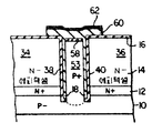
- 절연 영역을 갖고 있는 반도체 구조물에 있어서, 제1도전형의 반도체 기판, 상기 기판 상에 형성된어 있으며 제2도전형의 물질로 이루어진 반도체 재료층, 상기 반도체 재료층 내에 있고 이 층을 통하여 상기 기판까지 연장되어, 상기 반도체 재료층의 두 개의 반도체 영역을 그 대향하는 쪽에 각각 형성하기 위한 트렌치, 상기 트렌치를 채우고 이 트렌치의 저부에서 상기 기판과 전기적으로 접촉되는 도전성 반도체 물질, 상기 트렌치를 채우는 반도체 물질과 상기 반도체 재료층 사이에 형성되고 이 반도체 재료층의 외부 표면상에 적어도 부분적으로 측방향으로 연장되는 산화 장벽, 및 상기 트렌치를 채우는 물질의 상부와 전기적으로 접속되도록 형성된 상부 접속부를 포함하는 것을 특징으로 하는 반도체 구조물.
- 제17항에 있어서, 상기 산화 장벽과 상기 반도체 재료층 사이에 얇은 절연층을 더 포함하는 것을 특징으로 하는 반도체 구조물.
- 제17항에 있어서, 상기 반도체 재료층의 일면에 형성되고 상기 트렌치를 채우는 물질에 인접하여 상기 상부 접속부와 전기적으로 접속되는 반도체 영역을 더 포함하는 것을 특징으로 하는 반도체 구조물.
- 제17항에 있어서, 상기 상부 접속부가 회로 접지에 접속되는 것을 특징으로 하는 반도체 구조물.
- 제19항에 있어서, 상기 트렌치를 채우는 물질 및 상기 반도체 영역이 상기 제1도전형으로 형성되는 것을 특징으로 하는 반도체 구조물.
Applications Claiming Priority (3)
| Application Number | Priority Date | Filing Date | Title |
|---|---|---|---|
| US94574286A | 1986-12-22 | 1986-12-22 | |
| US945742 | 1986-12-22 | ||
| US945,742 | 1986-12-22 |
Publications (2)
| Publication Number | Publication Date |
|---|---|
| KR880008451A KR880008451A (ko) | 1988-08-31 |
| KR970000552B1 true KR970000552B1 (ko) | 1997-01-13 |
Family
ID=25483492
Family Applications (1)
| Application Number | Title | Priority Date | Filing Date |
|---|---|---|---|
| KR1019870014760A Expired - Fee Related KR970000552B1 (ko) | 1986-12-22 | 1987-12-21 | 기판의 표면 접촉부를 갖고 있는 딥 트렌치 분리 구조물 및 이의 제조 방법 |
Country Status (4)
| Country | Link |
|---|---|
| EP (1) | EP0272491B1 (ko) |
| JP (1) | JPS63168032A (ko) |
| KR (1) | KR970000552B1 (ko) |
| DE (1) | DE3752286T2 (ko) |
Families Citing this family (11)
| Publication number | Priority date | Publication date | Assignee | Title |
|---|---|---|---|---|
| JPH0254554A (ja) * | 1988-08-19 | 1990-02-23 | Fujitsu Ltd | 半導体装置およびその製造方法 |
| EP0398730A1 (en) * | 1989-05-19 | 1990-11-22 | Motorola Inc. | Method of forming planar isolation regions |
| US5643823A (en) * | 1995-09-21 | 1997-07-01 | Siemens Aktiengesellschaft | Application of thin crystalline Si3 N4 liners in shallow trench isolation (STI) structures |
| SE519975C2 (sv) * | 1999-06-23 | 2003-05-06 | Ericsson Telefon Ab L M | Halvledarstruktur för högspänningshalvledarkomponenter |
| JP2005142481A (ja) | 2003-11-10 | 2005-06-02 | Nec Electronics Corp | 半導体装置の製造方法 |
| JP4935219B2 (ja) | 2006-07-20 | 2012-05-23 | トヨタ自動車株式会社 | 排ガス浄化用触媒 |
| WO2009101870A1 (ja) * | 2008-02-12 | 2009-08-20 | Nec Corporation | 半導体装置 |
| JP4560100B2 (ja) * | 2008-03-24 | 2010-10-13 | 株式会社東芝 | 半導体装置 |
| CN108168743B (zh) * | 2017-12-20 | 2024-08-27 | 南京方旭智芯微电子科技有限公司 | 压力传感器及制造方法 |
| CN113991419B (zh) * | 2021-10-22 | 2023-12-15 | 中国科学院半导体研究所 | 掩埋异质结器件及其制备方法 |
| CN118398485B (zh) * | 2024-06-27 | 2024-09-13 | 合肥晶合集成电路股份有限公司 | 半导体器件的制备方法 |
Family Cites Families (4)
| Publication number | Priority date | Publication date | Assignee | Title |
|---|---|---|---|---|
| JPS5992548A (ja) * | 1982-11-18 | 1984-05-28 | Toshiba Corp | 半導体装置及びその製造方法 |
| US4528047A (en) * | 1984-06-25 | 1985-07-09 | International Business Machines Corporation | Method for forming a void free isolation structure utilizing etch and refill techniques |
| JPS61252644A (ja) * | 1985-05-01 | 1986-11-10 | Canon Inc | 半導体装置の製造方法 |
| US4728623A (en) * | 1986-10-03 | 1988-03-01 | International Business Machines Corporation | Fabrication method for forming a self-aligned contact window and connection in an epitaxial layer and device structures employing the method |
-
1987
- 1987-11-26 EP EP87117479A patent/EP0272491B1/en not_active Expired - Lifetime
- 1987-11-26 DE DE3752286T patent/DE3752286T2/de not_active Expired - Fee Related
- 1987-12-21 JP JP62323650A patent/JPS63168032A/ja active Pending
- 1987-12-21 KR KR1019870014760A patent/KR970000552B1/ko not_active Expired - Fee Related
Also Published As
| Publication number | Publication date |
|---|---|
| EP0272491B1 (en) | 1999-07-28 |
| DE3752286D1 (de) | 1999-09-02 |
| DE3752286T2 (de) | 2000-01-13 |
| EP0272491A3 (en) | 1989-03-15 |
| KR880008451A (ko) | 1988-08-31 |
| EP0272491A2 (en) | 1988-06-29 |
| JPS63168032A (ja) | 1988-07-12 |
Similar Documents
| Publication | Publication Date | Title |
|---|---|---|
| US4980747A (en) | Deep trench isolation with surface contact to substrate | |
| US4819052A (en) | Merged bipolar/CMOS technology using electrically active trench | |
| US6642581B2 (en) | Semiconductor device comprising buried channel region | |
| US5777370A (en) | Trench isolation of field effect transistors | |
| KR900005124B1 (ko) | 상보형 반도체장치 | |
| US4884117A (en) | Circuit containing integrated bipolar and complementary MOS transistors on a common substrate | |
| US5043778A (en) | Oxide-isolated source/drain transistor | |
| JP3691963B2 (ja) | 半導体装置及びその製造方法 | |
| US6518645B2 (en) | SOI-type semiconductor device and method of forming the same | |
| US4926233A (en) | Merged trench bipolar-CMOS transistor fabrication process | |
| US5920108A (en) | Late process method and apparatus for trench isolation | |
| US5374845A (en) | Process for reduced emitter-base capacitance in bipolar transistor | |
| US3943542A (en) | High reliability, low leakage, self-aligned silicon gate FET and method of fabricating same | |
| US6844223B2 (en) | Semiconductor device having silicon on insulator and fabricating method therefor | |
| JPH05102296A (ja) | 集積回路において平坦化した浅いトレンチ分離を製造する方法及びそれにより製造された構成体 | |
| US5049521A (en) | Method for forming dielectrically isolated semiconductor devices with contact to the wafer substrate | |
| US6180491B1 (en) | Isolation structure and method | |
| US4900689A (en) | Method of fabrication of isolated islands for complementary bipolar devices | |
| KR970000552B1 (ko) | 기판의 표면 접촉부를 갖고 있는 딥 트렌치 분리 구조물 및 이의 제조 방법 | |
| CN100373594C (zh) | 制造soi有源结构的方法和包括该结构的电路 | |
| US6222230B1 (en) | Method of making an elevated source/drain with enhanced graded sidewalls for transistor scaling integrated with spacer formation | |
| US5574306A (en) | Lateral bipolar transistor and FET | |
| US4720739A (en) | Dense, reduced leakage CMOS structure | |
| KR19990071491A (ko) | 적어도 하나 이상의 mos 트랜지스터를 가진 집적 회로장치를 제조하기 위한 방법 | |
| US5705440A (en) | Methods of fabricating integrated circuit field effect transistors having reduced-area device isolation regions |
Legal Events
| Date | Code | Title | Description |
|---|---|---|---|
| PA0109 | Patent application |
St.27 status event code: A-0-1-A10-A12-nap-PA0109 |
|
| R17-X000 | Change to representative recorded |
St.27 status event code: A-3-3-R10-R17-oth-X000 |
|
| PG1501 | Laying open of application |
St.27 status event code: A-1-1-Q10-Q12-nap-PG1501 |
|
| A201 | Request for examination | ||
| P11-X000 | Amendment of application requested |
St.27 status event code: A-2-2-P10-P11-nap-X000 |
|
| P13-X000 | Application amended |
St.27 status event code: A-2-2-P10-P13-nap-X000 |
|
| PA0201 | Request for examination |
St.27 status event code: A-1-2-D10-D11-exm-PA0201 |
|
| R17-X000 | Change to representative recorded |
St.27 status event code: A-3-3-R10-R17-oth-X000 |
|
| E902 | Notification of reason for refusal | ||
| PE0902 | Notice of grounds for rejection |
St.27 status event code: A-1-2-D10-D21-exm-PE0902 |
|
| T11-X000 | Administrative time limit extension requested |
St.27 status event code: U-3-3-T10-T11-oth-X000 |
|
| T11-X000 | Administrative time limit extension requested |
St.27 status event code: U-3-3-T10-T11-oth-X000 |
|
| P11-X000 | Amendment of application requested |
St.27 status event code: A-2-2-P10-P11-nap-X000 |
|
| P13-X000 | Application amended |
St.27 status event code: A-2-2-P10-P13-nap-X000 |
|
| G160 | Decision to publish patent application | ||
| PG1605 | Publication of application before grant of patent |
St.27 status event code: A-2-2-Q10-Q13-nap-PG1605 |
|
| E701 | Decision to grant or registration of patent right | ||
| PE0701 | Decision of registration |
St.27 status event code: A-1-2-D10-D22-exm-PE0701 |
|
| GRNT | Written decision to grant | ||
| PR0701 | Registration of establishment |
St.27 status event code: A-2-4-F10-F11-exm-PR0701 |
|
| PR1002 | Payment of registration fee |
St.27 status event code: A-2-2-U10-U11-oth-PR1002 Fee payment year number: 1 |
|
| PR1001 | Payment of annual fee |
St.27 status event code: A-4-4-U10-U11-oth-PR1001 Fee payment year number: 4 |
|
| PR1001 | Payment of annual fee |
St.27 status event code: A-4-4-U10-U11-oth-PR1001 Fee payment year number: 5 |
|
| PR1001 | Payment of annual fee |
St.27 status event code: A-4-4-U10-U11-oth-PR1001 Fee payment year number: 6 |
|
| PR1001 | Payment of annual fee |
St.27 status event code: A-4-4-U10-U11-oth-PR1001 Fee payment year number: 7 |
|
| PR1001 | Payment of annual fee |
St.27 status event code: A-4-4-U10-U11-oth-PR1001 Fee payment year number: 8 |
|
| PR1001 | Payment of annual fee |
St.27 status event code: A-4-4-U10-U11-oth-PR1001 Fee payment year number: 9 |
|
| PR1001 | Payment of annual fee |
St.27 status event code: A-4-4-U10-U11-oth-PR1001 Fee payment year number: 10 |
|
| PR1001 | Payment of annual fee |
St.27 status event code: A-4-4-U10-U11-oth-PR1001 Fee payment year number: 11 |
|
| FPAY | Annual fee payment |
Payment date: 20080103 Year of fee payment: 12 |
|
| PR1001 | Payment of annual fee |
St.27 status event code: A-4-4-U10-U11-oth-PR1001 Fee payment year number: 12 |
|
| LAPS | Lapse due to unpaid annual fee | ||
| PC1903 | Unpaid annual fee |
St.27 status event code: A-4-4-U10-U13-oth-PC1903 Not in force date: 20090114 Payment event data comment text: Termination Category : DEFAULT_OF_REGISTRATION_FEE |
|
| PC1903 | Unpaid annual fee |
St.27 status event code: N-4-6-H10-H13-oth-PC1903 Ip right cessation event data comment text: Termination Category : DEFAULT_OF_REGISTRATION_FEE Not in force date: 20090114 |
|
| P22-X000 | Classification modified |
St.27 status event code: A-4-4-P10-P22-nap-X000 |
|
| P22-X000 | Classification modified |
St.27 status event code: A-4-4-P10-P22-nap-X000 |