KR920010952B1 - Circuit and method of controlling operand buffer memory in data processing system - Google Patents
Circuit and method of controlling operand buffer memory in data processing system Download PDFInfo
- Publication number
- KR920010952B1 KR920010952B1 KR1019890000777A KR890000777A KR920010952B1 KR 920010952 B1 KR920010952 B1 KR 920010952B1 KR 1019890000777 A KR1019890000777 A KR 1019890000777A KR 890000777 A KR890000777 A KR 890000777A KR 920010952 B1 KR920010952 B1 KR 920010952B1
- Authority
- KR
- South Korea
- Prior art keywords
- instruction
- command
- address
- buffer memory
- load
- Prior art date
Links
- 239000000872 buffer Substances 0.000 title claims abstract description 152
- 238000012545 processing Methods 0.000 title claims abstract description 36
- 238000000034 method Methods 0.000 title claims abstract description 22
- 230000007246 mechanism Effects 0.000 claims description 31
- 239000003550 marker Substances 0.000 claims description 19
- 230000002441 reversible effect Effects 0.000 claims description 17
- XEEYBQQBJWHFJM-UHFFFAOYSA-N Iron Chemical compound [Fe] XEEYBQQBJWHFJM-UHFFFAOYSA-N 0.000 claims description 14
- 238000012360 testing method Methods 0.000 claims description 10
- 229910052742 iron Inorganic materials 0.000 claims description 7
- FVJPPEWHZCSTAC-UHFFFAOYSA-N meta-O-Dealkylated flecainide Chemical compound OC1=CC=C(OCC(F)(F)F)C(C(=O)NCC2NCCCC2)=C1 FVJPPEWHZCSTAC-UHFFFAOYSA-N 0.000 claims description 7
- 230000003111 delayed effect Effects 0.000 claims description 6
- 101150116491 SUC7 gene Proteins 0.000 claims description 5
- 230000009191 jumping Effects 0.000 claims description 5
- 230000004044 response Effects 0.000 claims description 5
- 238000012546 transfer Methods 0.000 claims description 4
- 101100033673 Mus musculus Ren1 gene Proteins 0.000 claims description 3
- 101100033674 Mus musculus Ren2 gene Proteins 0.000 claims description 3
- 101710136899 Replication enhancer protein Proteins 0.000 claims description 3
- 235000000396 iron Nutrition 0.000 claims description 3
- 238000005516 engineering process Methods 0.000 claims description 2
- 238000012937 correction Methods 0.000 claims 2
- 238000003780 insertion Methods 0.000 claims 1
- 230000037431 insertion Effects 0.000 claims 1
- 238000010586 diagram Methods 0.000 description 7
- 210000004027 cell Anatomy 0.000 description 4
- PMVSDNDAUGGCCE-TYYBGVCCSA-L Ferrous fumarate Chemical compound [Fe+2].[O-]C(=O)\C=C\C([O-])=O PMVSDNDAUGGCCE-TYYBGVCCSA-L 0.000 description 3
- 230000005540 biological transmission Effects 0.000 description 3
- 230000001960 triggered effect Effects 0.000 description 3
- 230000001934 delay Effects 0.000 description 2
- 238000013461 design Methods 0.000 description 2
- 230000006870 function Effects 0.000 description 2
- 230000036316 preload Effects 0.000 description 2
- 230000008569 process Effects 0.000 description 2
- 210000000352 storage cell Anatomy 0.000 description 2
- 241001515642 Opium poppy mosaic virus Species 0.000 description 1
- 230000008859 change Effects 0.000 description 1
- VJTAZCKMHINUKO-UHFFFAOYSA-M chloro(2-methoxyethyl)mercury Chemical compound [Cl-].COCC[Hg+] VJTAZCKMHINUKO-UHFFFAOYSA-M 0.000 description 1
- 238000012790 confirmation Methods 0.000 description 1
- 230000008878 coupling Effects 0.000 description 1
- 238000010168 coupling process Methods 0.000 description 1
- 238000005859 coupling reaction Methods 0.000 description 1
- 238000013075 data extraction Methods 0.000 description 1
- 238000011156 evaluation Methods 0.000 description 1
- 230000036541 health Effects 0.000 description 1
- 230000000977 initiatory effect Effects 0.000 description 1
- 238000011835 investigation Methods 0.000 description 1
- 238000012544 monitoring process Methods 0.000 description 1
- 238000002360 preparation method Methods 0.000 description 1
- 102200059233 rs754995756 Human genes 0.000 description 1
- 238000004088 simulation Methods 0.000 description 1
- 230000002123 temporal effect Effects 0.000 description 1
Images


Classifications
-
- G—PHYSICS
- G06—COMPUTING; CALCULATING OR COUNTING
- G06F—ELECTRIC DIGITAL DATA PROCESSING
- G06F13/00—Interconnection of, or transfer of information or other signals between, memories, input/output devices or central processing units
- G06F13/38—Information transfer, e.g. on bus
-
- G—PHYSICS
- G06—COMPUTING; CALCULATING OR COUNTING
- G06F—ELECTRIC DIGITAL DATA PROCESSING
- G06F9/00—Arrangements for program control, e.g. control units
- G06F9/06—Arrangements for program control, e.g. control units using stored programs, i.e. using an internal store of processing equipment to receive or retain programs
- G06F9/30—Arrangements for executing machine instructions, e.g. instruction decode
- G06F9/38—Concurrent instruction execution, e.g. pipeline, look ahead
- G06F9/3802—Instruction prefetching
- G06F9/3808—Instruction prefetching for instruction reuse, e.g. trace cache, branch target cache
- G06F9/381—Loop buffering
-
- G—PHYSICS
- G06—COMPUTING; CALCULATING OR COUNTING
- G06F—ELECTRIC DIGITAL DATA PROCESSING
- G06F9/00—Arrangements for program control, e.g. control units
- G06F9/06—Arrangements for program control, e.g. control units using stored programs, i.e. using an internal store of processing equipment to receive or retain programs
- G06F9/30—Arrangements for executing machine instructions, e.g. instruction decode
- G06F9/30003—Arrangements for executing specific machine instructions
- G06F9/3005—Arrangements for executing specific machine instructions to perform operations for flow control
- G06F9/30069—Instruction skipping instructions, e.g. SKIP
-
- G—PHYSICS
- G06—COMPUTING; CALCULATING OR COUNTING
- G06F—ELECTRIC DIGITAL DATA PROCESSING
- G06F9/00—Arrangements for program control, e.g. control units
- G06F9/06—Arrangements for program control, e.g. control units using stored programs, i.e. using an internal store of processing equipment to receive or retain programs
- G06F9/30—Arrangements for executing machine instructions, e.g. instruction decode
- G06F9/32—Address formation of the next instruction, e.g. by incrementing the instruction counter
- G06F9/322—Address formation of the next instruction, e.g. by incrementing the instruction counter for non-sequential address
- G06F9/325—Address formation of the next instruction, e.g. by incrementing the instruction counter for non-sequential address for loops, e.g. loop detection or loop counter
-
- G—PHYSICS
- G06—COMPUTING; CALCULATING OR COUNTING
- G06F—ELECTRIC DIGITAL DATA PROCESSING
- G06F9/00—Arrangements for program control, e.g. control units
- G06F9/06—Arrangements for program control, e.g. control units using stored programs, i.e. using an internal store of processing equipment to receive or retain programs
- G06F9/30—Arrangements for executing machine instructions, e.g. instruction decode
- G06F9/38—Concurrent instruction execution, e.g. pipeline, look ahead
- G06F9/3802—Instruction prefetching
- G06F9/3814—Implementation provisions of instruction buffers, e.g. prefetch buffer; banks
Landscapes
- Engineering & Computer Science (AREA)
- Theoretical Computer Science (AREA)
- Software Systems (AREA)
- Physics & Mathematics (AREA)
- General Engineering & Computer Science (AREA)
- General Physics & Mathematics (AREA)
- Advance Control (AREA)
- Executing Machine-Instructions (AREA)
- Communication Control (AREA)
- Memory System Of A Hierarchy Structure (AREA)
Abstract
Description
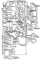
제1도는 데이터처리장치의 개략구성도.1 is a schematic configuration diagram of a data processing apparatus.
제2도는 버퍼제어장치의 블록도.2 is a block diagram of a buffer control apparatus.
제3도는 명령계수회로의 블록도.3 is a block diagram of a command coefficient circuit.
제4도는 버퍼기억장치의 블록도.4 is a block diagram of a buffer memory device.
제5도는 기억셀의 회로도이다.5 is a circuit diagram of a memory cell.
*도면의 주요부분에 대한 부호의 설명* Explanation of symbols for main parts of the drawings
IBUF : 명령버퍼기억장치 AP,FA : 부하지시 애드레스IBUF: Command Buffer Memory AP, FA: Load Address
BRA : 명령 애드레스 MEM : 주기억장치BRA: Command Address MEM: Main Memory
IDEC : 명령 디코우더IDEC: Command Decoder
본 발명은 프로그램경과에 응해서 연속적으로 높여져야 할 명령애드레스에 대해서 최대 소정차 만큼 이명령 애드레스보다 선행해서 높여지는 부하지시애드레스에 의해 제어되고, 명령어가 주기억장치로부터 명령 버퍼기억장치안으로 연이어 부하되어, 이 명령버퍼기억장치로 부터 명령이 명령애드레스에 의해 나중에 애드레스지정 되어서, 실행을 위해 명령디코우더로 공급되는, 데이터처리장치에서의 명령버퍼기억장치의 회로 및 제어방법에 관한 것이다.The present invention is controlled by a load address that is raised before this command address by a predetermined amount up to a command address that must be continuously raised in response to a program passage, and the instruction is continuously inserted into the command buffer storage device from the main memory. A circuit and control method for a command buffer memory in a data processing device, which are loaded and supplied from the command buffer memory later by the address of the command and supplied to the command decoder for execution. will be.
잡지「컴퓨터·디자인」(1987년 8월 1일)89페이지 및 다음 페이지 이하「가장 우수한 기억장치를 선택하는 것에 의한 최대한의 성능」에, 모든 공지의 타일 기억장치 및 그 제어방법이 표시되어 있다.89 pages of the magazine Computer Design (August 1, 1987) and the following pages, "Maximum performance by selecting the best storage device", shows all known tile storage devices and their control methods. .
미국특허 제3611315호 명세서로 부터 프로그램이 프로세서의 입력 및 출력데이터와 함께 주기억장치에 기억되어 있는, 프로그램 제어되는 데이터처리장치에 있어서, 실행을 위해 내어놓은 프로그램의 명령순서를 주기억장치로 부터 버퍼기억장치로 타일마다 한층 짧은 액세스타임으로 전송하여서 이 버퍼기억장치로부터 명령데코오터로 공급하는 것은 공지이고, 이 경우, 실행을 위해 내어지는 명령의 명령애드레스는 버퍼기억장치에 포함되어 있는 명령의 애드레스 범위와 비교되어서 애드레스지정되어야 할 명령이 버퍼기억장치에 포함되어 있는 한, 이를 구한 명령이 1개의 타일길이의 부속명령순서로 주기억장치로 부터 버퍼기억장치의 타일에 부하되어서 명령이 거기에 부하된 후에 거기에 애드레스 지정되어서 명령디코우더로 공급되어서 실행되어, 그때 당연한 명령 알아내기는 다음의 명령애드레스가 명령계수기 상태의 프로그램에 관계하는 변화에 의해 얻어진 후에, 행하여진다.In a program-controlled data processing apparatus in which a program is stored in a main memory together with input and output data of a processor from US Patent No. 3611315, the instruction order of a program issued for execution is stored in the main memory. It is well known to transmit a device with a shorter access time for each tile and supply it from the buffer memory to the instruction decorator. In this case, the instruction address of the instruction issued for execution is added to the instruction contained in the buffer memory. As long as the instruction that needs to be addressed as compared to the address range is included in the buffer storage, the instruction obtained is loaded from the main memory into the tiles of the buffer storage in the order of one tile length subcommand. After loading, it is addressed and supplied to the command decoder for execution. Air, after that time, the next instruction add less bet out granted command obtained by the change relating to the status of the instruction program counter, it is carried out.
이 회로에는, 명령순거가 타일의 크기에 응해서 특정의 전송시간이 필요하게 되어, 그 결과 가끔 기다리는 시간이 생겨, 이들 기다리는 시간은, 구해지는 명령의 앞의 타이 위에 있고 또는 명령으로의 프로그램의 분기후에 타일의 외부에 생기는, 가끔 필요하지 않은 각개 명령의 경과 경우의 전송때문에 소비된다는 결점이 있다. 그위에 이와같은 필요치 않은 명령의 전송중에 주기억장치로 필요한 데이터액세스가 방해받는다.This circuit requires a specific transfer time depending on the order of the tiles depending on the size of the tile, resulting in occasional waiting time, which is on the tie before the instruction to be found or the branch of the program to the instruction. The drawback is that it is consumed because of the transmission of the elapsed time of each command that sometimes happens outside the tile. On top of that, accessing the necessary data to the main memory is interrupted during the transmission of these unwanted commands.
더우기 명령액세스때의 평균 기다리는 시간을 단축하기 위하여 실행되어야 할 명령에 의해 기억되어 있는 특정수의 명령을 이미 조기에 선취명령버퍼기억장치에 전송하고, 이 명령버퍼기억장치로 부터 명령이 명령해독을 위해 읽어내는 것은 잡지「컴퓨터·디자인」제21권(1982년 4월) 64페이지로 부터 공지이다. 그러나 프로그램 분기가 행하여지는 경우는 새로운 주기억장치액세스에 대해 기다리는 시간이 생겨 이 주기억장치는 경치는 앞부하를 받고 이는 동시에 필요한 데이터액세스를 방해한다.Furthermore, in order to reduce the average waiting time for command access, a certain number of commands already stored by the command to be executed are sent to the preemptive command buffer memory early, and the command decodes from the command buffer memory. For the purpose of reading this article, please read page 64 of the magazine, Computer Design, Vol. 21 (April 1982). However, when a program branch is made, there is time to wait for a new main memory access, which causes the landscape to be loaded at the same time, which at the same time hinders necessary data access.
이것은 특히 프로그램이 루프를 이루어서 몇번이고 또는 순환적으로 행하여지는 경우에 커다란 결점이며, 이 경우, 명령은 적당한 액세스부하를 갖는 주기억장치로 부터 반복해서 새롭게 떼어내어지지 않으면 안된다. 왜냐하면 루-프의 개시때의 분기할때에는 언제나 프로그램부분의 최초의 명령의 인수에 의한 프로그램 경과중의 부하 지연이 생기기 때문이다.This is a major drawback, especially if the program is executed repeatedly or repeatedly in a loop, in which case the instruction must be repeatedly detached from the main memory with the appropriate access load. This is because there is always a load delay in the course of the program due to the argument of the first instruction in the program section at the time of branching at the beginning of loop.
본 발명의 과제는 프로그램 경과중의 부하 지연의 수 및 주기억장치의 액세스부하를 프로그램 경과중의 명령버퍼 기억장치로의 액세스부하를 프로그램 경과중의 명령버퍼 기억장치로 명령전송의 수의 감소에 의해 작게하는 명령버퍼기억장치의 회로장치 및 이 회로장치의 작동방법을 제공하는 것이다.The problem of the present invention is that the number of load delays during the passage of the program and the access load of the main memory to the instruction buffer storage during the passage of the program is reduced by reducing the number of command transfers to the instruction buffer storage during the passage of the program. It is to provide a circuit device of a command buffer memory device to be reduced and a method of operating the circuit device.
이 과제의 해결책은 명령버퍼기억장치가, 연이어 부하되어, 이미 실행되어 또는 뛰어 넘겨진 명령어가 남아 있는 명령보류기억장치 만큼 확대되어 있어, 프로그램 경과중에 분기명령의 명령애드레스부에 생기는 분기애드레스가 명령버퍼기억장치에 포함되어 있는, 즉 앞부하되어서 보호유지된, 명령어의 각각의 애드레스 범위와 비교되어, 분기 애드레스가 이 애드레스 범위 내에 있는 경우는 이 분기애드레스에 의해 애드레스 지정된 명령이 직접명령버퍼기억장치로 부터 읽어내고, 그리고 분기 애드레스가 상술의 애드레스 범위 밖에 있는 경우는 이 분기 애드레스가 새로운 부하지시기로써 인수되어서 오래된 애드레스범위가 소거된다는 것이다.The solution of this problem is that the instruction buffer memory is expanded as much as the instruction hold memory in which the instruction which has been loaded in succession and already executed or jumped over remains. The address specified by this branch address if the branch address is within this address range compared to the respective address ranges of the instructions contained in the instruction buffer memory, i.e., loaded and protected. Reading from this direct instruction buffer, and if the branch address is outside the address range described above, the branch address is taken over as a new load time and the old address range is erased.
또한 보류 버퍼기억장치가 선취버퍼기억장치와 양자가 순환적 작동으로 공통의 트리거(trigger)수단에 의해 작동될 수 있는 것같이, 명령버퍼기억장치에 통합되어 있다.The pending buffer memory is also incorporated into the command buffer memory, as both the preemptive buffer memory and both can be operated by a common trigger means in a circular operation.
명령버퍼기억장치가 연산기구의 데이터입력단의 앞에 접속되어있는 레지스터셋트로 부터 분리되어, 그 결과 동시에 새로운 명령이 읽어내고 따라서 데이터에 의해 조작될 수 있는 경우는 특히 유리하다.It is particularly advantageous if the instruction buffer memory is separated from the register set connected in front of the data input end of the computing device, so that a new instruction can be read at the same time and thus manipulated by the data.
본 발명에 의한 명령 액세스로 부터의 주기억장치의 부가제거는 주기억장치가 페이지마다 조직되어, 페이지의 선택이 1개의 페이지에 있어서의 페이지액세스타임보다 긴 페이지교환을 갖는 경우에 특히 유리하게 작용한다.The addition and removal of the main memory from the instruction access according to the present invention is particularly advantageous when the main memory is organized page by page, so that the selection of pages has a page exchange longer than the page access time in one page.
시판의 기억장치에는 액세스타임의 이 비는 약 4대 1이다. 데이터 및 명령은 일반적으로 다른 페이지에서 처리되지 않으면 안되므로, 명령을 버퍼기억장치로부터 떼어냄에 따라 주기억장치로부터 떼어내어 지지 않은 경우는 페이지의 교환이 생략될 수 있다.In commercially available storage, this ratio of access time is about four to one. Since data and instructions must generally be processed in different pages, the exchange of pages can be omitted if the instructions are removed from the main memory as the instructions are removed from the buffer memory.
특히 복수의 기계펄스 싸이클에 상당하는 긴 페이지액세스타임때문에 주기억장치로 부터 요구됨에 따라 나중에 가서 처음 나오는 정보의 목표애드레스용의 소위 파이프라인을 주기억장치에 대응시키는 것은 보통 행하여지고 있다. 이들 정보는 데이터 레지스터 셋트로부터 분리된 명령 버퍼기억장치를 갖는 본 발명에 의한 장치에 있어서, 데이터 또는 명령이냐에 응해서, 애드레스에 관계해서 레지스터 셋트 또는 명령버퍼기억 장치로 공급된다.In particular, as long as the page access time corresponding to a plurality of mechanical pulse cycles is required from the main memory, it is usually done to correspond to the main memory so-called pipelines for the target address of information which comes out later. In the apparatus according to the present invention having an instruction buffer storage device separated from the data register set, the information is supplied to the register set or the command buffer storage device in relation to the address depending on whether the data or the command is used.
명령버퍼기억장치에 아직 포함되어 있지 않은 실행되어야 할 명령의 애드레스가 명령을 받는 준비가 되어있는 경우는, 그 애드레스가 예를들면 애드레스 퍼이프라인에 포함되어 있는지 아닌지를 시험회로에서 부가적으로 조사, 혹시 포함되어 있으면 명령버퍼기억장치로의 명령의 기억을 기다리는 것이 유리하다.If the address of a command to be executed that is not already included in the command buffer memory is ready to receive the command, the test circuit adds, for example, whether or not the address is included in the address ppuline. In general, it is advantageous to wait for the memory of the command to the command buffer memory if it is included in the investigation or if it is included.
또다른 유리한 구성은 특별한 명령, 즉 앞부하 명령이 설치되어 있고, 이명령이 명령에 설정된 수의 명령어의 버퍼기억장치로 전송을 제어하는 것이다.Another advantageous configuration is to install a special command, i.e. a load command, which controls the transfer to the buffer storage of the number of instructions set in the command.
소정수의 명령어는 반어(半語)에 관한 명령으로 표시되어 따라서 명령어의 전송을 할때에 필요에 따라 다음 전어(全語)한계로 매듭된다.A predetermined number of commands are indicated as commands related to the ironic words, and thus, when the command is transmitted, they are knotted to the next word limit as necessary.
한층 큰수의 주기억장치 데이터명령이 순차로 이어지는 경우는 앞부하 명령이 유리하게 사용된다. 왜냐하면 명령실행때의 명령페이지와 데이터페이지와의 한층 번잡한 페이지 교환이 회피되기 때문이다. 다시 말하면 이 경우는 중간 접속된 명령 액세스가 벌써 행하여 지지 않기 때문이다.In the case where a larger number of main memory data commands follow sequentially, the front load command is advantageously used. This is because a more complicated page exchange between the command page and the data page at the time of command execution is avoided. In other words, this is because the intermediate-connected command access is not already performed.
더욱이, 버퍼모드마아커는 프로그램중에서 설정 및 소거가능한 것이 유리하다. 이 버퍼모드마아커는 루우프안에 상대 애드레스를 갖는 순방향(順方向)뛰어넘는 명령의 목표명령이 아직 버퍼기억장치에 없는 경우에 우선 순방향 뛰어넘기 분기가 행하여져, 이어 목표애드레스까지의 명령순서가 명령 버퍼기억장치로 부하될때 까지의 사이에 기다려져 이에 의해서, 더이상의 명령부호 및 선행이 행하여 지기 전에 전루우프가 거기에 우선 완전하게, 몇번의 실행의 준비를 하고, 존재하고 있는 것을 보증한다. 더욱이, 버퍼모드마아커에의해 초기 범위가 경우에 따라 뛰어 넘겨지는 명령순서가 완전히 부하되어 따라서 이렇게 지연이 없는 몇번의 실행준비가 이루어지는 것이 보증된다.Moreover, it is advantageous that the buffer mode markers can be set and erased in the program. In this buffer mode marker, if a target instruction of a forward skipping instruction having a relative address in the loop is not yet present in the buffer storage, a forward skip branch is performed first, and then the instruction sequence to the target address is performed. It waits until it is loaded into the instruction buffer memory, thereby ensuring that all the loops are completely prepared there several times before the further instruction codes and preceding ones are carried out and are present. Furthermore, the buffer mode markers ensure that the instruction sequence in which the initial range is jumped from case to case is fully loaded, thus ensuring that several execution preparations are made without this delay.
앞부하명령 및 버퍼모도마아커의 설정을 위한 명령은, 상술의 기준이 존재하는 경우에 콤바일러 프로그램에 의해 명령순서에 넣어지는 것이 유리하다.The command for setting the front load instruction and the buffer mode marker is advantageously put into the instruction sequence by the combiner program when the above-mentioned criteria exist.
또다른 유리한 구성은 명령 기억용량을 한층 양호하게 이용하기 위하여, 되도록이면 1개 내지 3개의 반어(半語)를 갖는 가변의 언어길이의 명령이 사용되어, 이들 반어가 서로 이어서 전어(全語)의 형태로 기억되어, 그 경우 버퍼기억장치가, 전어(全語)가 이 버퍼기억장치에 써서 넣어지지만, 그러나 명령이 위치가 올바른 명령 및 애드레스 부분을 갖는 버퍼로 부터 명령 데크오더로 공급되도록, 구성되어 있다는 것에 있다.Another advantageous configuration is that variable language length instructions having as much as one to three ironic words are used, in order to better utilize the instruction memory, such that the ironic words are followed by whole words. In this case, so that the buffer memory is written to this buffer memory, but the instruction is supplied to the instruction deck order from a buffer with the correct position of the instruction and address. In that it is constructed.
버퍼기억장치를 다중독해를 하는 반어기억장치로써 유리하게 구성하는 것은, 명령으로의 지연이 없는 액세스를 가능하게 함에 따라 나중에 접속된 부분어가 빠지게 또는 복수회의 액세스를 불필요로 한다.Advantageously constructing the buffer memory as an ironic memory device for multi-reading allows access without delay to the instruction, thereby eliminating later access to subwords or unnecessary multiple times of access.
본 발명의 이러한 동작을 구현하는 실시예를 제1도 내지 제5도에 도시하였다. 제1도에 데이터처리장치가 블록도로 표시되어 있고, 이 데이터처리장치의 데이터 및 프로그램은 주기억장치 MEM에 기억되어 있고, 이들 데이터 및 프로그램은 기억장치 데이터버스 MDB를 거쳐서 기억장치제어기구 MEMC에 관계해서 레지스터셋트 RGST로 공급됨에 따라 거기에서 2개의 데이터버스 XDB,YDB플 거쳐서 연산기구 ALU로 또는 기억장치 데이터버스 MDB로 부터 버퍼기억장치 DIBUF로, 또 이 버퍼기억장치로 부터 해독(解讀)제어되어서 명령 디코우더 IDEC로, 또 이 명령디코우더로 부터 명령제어기구 EXEC로 공급된다. 이들 명령은 레지스터 셋트 RGST와 접속되어 있는 명령 애드레스기구 PCU에 의해 연이어 명령 애드레스 신호PCS 거처서 버퍼기억장치 BUF로 부터 해독되어 이들의 명령신호 IS는 명령디코우더 IDEC로 공급된다.Embodiments for implementing this operation of the present invention are shown in FIGS. A data processing apparatus is shown in block diagram in FIG. 1, and data and programs of this data processing apparatus are stored in the main memory MEM, and these data and programs are related to the storage control mechanism MEMC via the storage data bus MDB. Is supplied to the register set RGST from there through two data buses XDB and YDB to the computing device ALU or from the storage device data bus MDB to the buffer storage device DIBUF and from this buffer storage device. It is supplied to the command decoder IDEC and from this command decoder to the command control mechanism EXEC. These instructions are subsequently decoded from the buffer memory BUF via the instruction address signal PCS via the instruction address mechanism PCU connected to the register set RGST, and their instruction signals IS are supplied to the instruction decoder IDEC.
또한 이들 명령애드레스 신호 PCS는 명령부하 회로 PPU로 공급되어 이 명령부하 회로는 다시 명령제어기구 EXEC로 부터 특별명령 실행을 위한 명령제어신호 FS를 받아 따라서 상태신호 및 제어신호, 즉 분기제어신호 BCS, 파이프라인 부하신호 PLC 및 부속의 상태신호를 애드레스파이프라인 APL의 명령제어기구 EXEC 및 기억장치제어기구 MEMG와 교환한다.In addition, these command address signals PCS are supplied to the command load circuit PPU, and the command load circuit receives the command control signal FS for execution of a special command from the command control mechanism EXEC, and thus the status signal and the control signal, that is, the branch control signal BCS. For example, exchange the pipeline load signal PLC and the attached status signal with the command control mechanism EXEC of the address pipeline APL and the memory control mechanism MEMG.
애드레스파이프라인 APL은 레지스터 부하 애드레스 RA 또는 버퍼부하 애드레스 FA를 수용해 또 이들 부하 애드레스를 레지스터 써넣기 애드레스 RWA로서 레지스터 써넣기 신호 RWC와 함께 또는 버퍼 써넣기 애드레스 IBA로써 버퍼 써넣기 신호 IBW와 함께 레지스터 셋트 RGST 또는 버퍼기억장치 IBUF로 지연되어 발한다.The addressless pipeline APL accepts register load address RA or buffer load address FA and writes these load addresses with register write signal RWC as register write address RWA or buffer write signal IBW with buffer write address IBA. Along with register set RGST or buffer storage IBUF, delays occur.
이 지연은 주기억장치데이터 빼어내기 시간에 상당하며 이 주기억장치 데이터 빼어내기 시간은 기억장치 애드레스 인도와 동시에 기억장치 감시 신호 MCS를 거쳐서 개시된다. 그 때문에, 부속의 주기억장치 애드레스는 기억장치 애드애드레스버스 ADB를 거쳐서 연산기구 ALU 또는 명령부하회로 PFU로 부터 기억장치 애드레스 레지스터 MEMAR에 주어지며, 이 기억장치 애드레스 레지스터로 부터 주기억장치애드레스는 페이지 애드레스 버스 PAB 및 행(行)애드레스버스 RAB를 거쳐서 주기억장치 MEM으로 공급된다.This delay corresponds to the main memory data extraction time, which is initiated via the storage monitoring signal MCS at the same time as the storage address delivery. Therefore, the attached main memory address is given to the storage address register MEMAR from the computing mechanism ALU or the instruction load circuit PFU via the storage add address bus ADB, and the main memory add from the storage address register. The address is supplied to the main memory MEM via the page address bus PAB and the row address bus RAB.
연산기구 ALU에서 산출된 결과는, 결과 데이터버스 ZDB를 거쳐서 레지스터 셋트 RGST로 되돌아 가게되어 또는 써넣기 데이터버스 WDB 및 써넣기 레지스터 STDR을 거쳐서 기억장치 데이터버스 MDB로 공급되어, 또 이렇게 주기억장치로 되돌아 가게 하기 위해 기억장치 제어기구 MEMG로 공급된다.The result calculated by the computing unit ALU is returned to the register set RGST via the result data bus ZDB or supplied to the storage data bus MDB via the write data bus WDB and the write register STDR, and thus returned to the main memory. To the storage control mechanism MEMG.
연산기구 ALU의 제어는 명령제어신호 OCS를 거쳐서 상태신호 STS에 관계해서 행하여 진다. 뛰어넘기 명령애드레스는 명령분기의 경우에 결과 데이터버스 ZDB를 거쳐서 명령계수기기 PCU 및 명령부하회로 PFU로 보내어진다.The control of the computing mechanism ALU is performed in relation to the status signal STS via the command control signal OCS. The jumping instruction address is sent to the instruction counting unit PCU and the instruction load circuit PFU via the resulting data bus ZDB in the case of the instruction branch.
명령부하회로 PFU의 상세한 것이 제2도에 표시되어 있다. 회로를 통하는 데이터의 흐름은 도시 되지않은 2개의 진도 순서에 의해 교대로 발생하게 된다. 진도 순서에 의해 트리거되는, 레지스터 및 플립플롭(flip-flops)은 제2도의 진도순서에 의해 트리거 되는 레지스터 및 플립플롭과는 부호의 최후의「V」로 구별된다. 표시문자에 붙어있는 숫자는 레지스터 또는 가산기구의 출력단에 있어서의 결과의 2진수의 신호의 위치를 표시하고 있다. 최후의「N」은 반전된 신호를 표시하고 있다.The details of the command load circuit PFU are shown in FIG. The flow of data through the circuit alternately occurs in two magnitude sequences, not shown. Registers and flip-flops, triggered by the magnitude order, are distinguished from registers and flip-flops triggered by the magnitude order of FIG. The number attached to the display character indicates the position of the resulting binary signal at the output of the register or adder. The last "N" indicates an inverted signal.
표시문자의 최후 또는 최후로부터 2번째의 위치에 있는「F」는 플립플롭인 것을 표시하고 있다. 설명중에 신호의 논리 결합을 위한 공식이 예거되어 있는 경우는,「」기호는 논리 AND회로를 표시하고,「V」기호는 논리 OR회로를 표시하고 있다. 공식중에 표시되어 있는 량은, 표시된 회로소자의 출력단에 생겨 따라서 서로 위치적으로 올바르게 결합되어서 다음의 기계 펄스에서 회로소자로 전송되어 이들 회로소자는 결과의 화살표에 응해서 표시되어 있다. 도시한 회로장치에서는 버퍼기억장치의 크기가 16비트의 64의 반어라고 가정되어 있으므로 버퍼 기억장치의 해독애드레스는 6비트의 길이이다."F" at the end of the display character or the second position from the end indicates that it is a flip-flop. When the formula for logical coupling of signals is illustrated in the description, the symbol "" denotes a logic AND circuit, and the symbol "V" denotes a logical OR circuit. The quantities indicated in the formula are generated at the output of the displayed circuitry and are therefore correctly positionally coupled to each other and transferred to the circuitry at the next mechanical pulse so that these circuitry is displayed in response to the resulting arrow. In the circuit device shown, it is assumed that the size of the buffer memory device is 64 ironic bits of 16 bits. Therefore, the decoding address of the buffer memory device is 6 bits long.
명령이 전어의 형태로 묶여져서 기억되기 때문에, 써넣기 애드레스 지정 때문에 장소 2 내지 6밖에 이용되고 있지 않다. 최저치의 장소는 “0”으로 표시되어 었다. 이 장소는 바이트(Bite)위치 결정을 위하여 사용되므로, 이 장소는 여기서는 기능이 없다. 버퍼기억장치를 제어하기 위하여 명령계수기 신호 PCV가 제어장치로 도입되는 명령계수기 말고, 2개의 지시레지스터, 즉 부하지시가산기 CTA와 부하지시보조 레지스터 APV를 갖는 30비트(bit)의 부하지시 레지스터 AP 및 역방향지시 가산기 CTB와 역방향 지시레지스터 BP가 이용된다. 명령버퍼 기억장치의 외부에 있는 애드레스의 분기 명령에 있어서, 명령계수기 내용 및 양 지시기는 같은 값으로 설정되어, 그 때문에 부하 멀티플랙서 MPXB, MPXB, MPXA가 AND게이트 회로 GB의 출력신호를 거쳐서 결과 데이터버스 ZDB에 접속되어, 이 출력신호는 뛰어 넘기 명령신호 BR 및 분기신호 BRCAPV의 작용을 받는다. 부하시 례지스터 AP는 비트 2 내지 31의 주기억장치의 완전한 애드레스에 설계되어 있어, 역방향지시 레지스터 BP는 그냥 버퍼기억장치의 길이에 응해서 비트 2 내지 6에 설계되어 있다. 각 명령해독전, 명령이 이미 명령 버퍼기억장치에 넣어져 있는지 아닌지 조사된다. 그 때문에 명령애드레스신호 PCV7-2로부터 제1의 가산기구 SUB, SUA의 지시기의 후부의 비트가 감해져 그때 명령버퍼 기억장치에 포함되어 있는 면저 부하된 언어 COMPAV의 부수 및 보류된 언어 CMPBV의 수가 형성된다. 분기 명령이 실행되는 경우를 위하여 반어의 형태로 표시되어 있는 뛰어넘기폭 OPRV, OPMV는 제2의 가산기구 SUD, SUC에서 정정숫자1 및 명령계수신호 PCV1의 최후의 장소와 함께 산출된 언어수에 가산되므로 발생하는 잉여 SUC7,SUD7은 분기목표가 명령버퍼기억장치에 포함되어 있는지 아닌지를 표시하고 이에 의거하여 이 분기는 직접 실행되어 또는 그 애드레스가 이미 애드레스 파이프라인에 존재하는 경우는 분기가 실행되어 따라 버퍼기억장치로의 목표명령어의 기억때까지 기다려져, 그후, 이 목표 명령어는 명령다코우더에 읽혀진다.Since the commands are stored in the form of words, they are only used in
여러가지의 분기 명령의 제어신호 및 잉여신호 DUC7, SUD7은 분기 평가회로 BRCALV, BRCHL안에서 나중에 접속된 플립플롭 BRCAF, BRCAFV를 갖는 2개의 시간적 단계로 확인되므로 출력신호 BRCAFV는 분기의 실행을 개시시켜 또는 버퍼부하의 새로운 개시를 불러 일으킨다.The control signals of the various branch instructions and the surplus signals DUC7 and SUD7 are identified in two temporal steps with flip-flops BRCAF and BRCAFV connected later in the branch evaluation circuits BRCALV and BRCHL, so that the output signal BRCAFV initiates the execution of the branch or buffers. Causes a new initiation of the load.
이 때문에 뛰어넘기 애드레스는 분기 플립플롭 BRCAFV가 셋트되어 있는 경우에 명령계수기구에만 전송된다.For this reason, the skip address is only transmitted to the instruction counting mechanism when the branch flip-flop BRCAFV is set.
다른 경우에는 이 뛰어넘기 애드레스는 지시 레지스터 AP, BP에도 전송되어 명령해독이 개시된다.In other cases, this skip address is also sent to the indication registers AP and BP to initiate command decryption.
분기 제어회로(BRCALV, BRCHL)는 상세하게 말하면 다음과 같은 결합을 포함하고 있다.In detail, the branch control circuits BRCALV and BRCHL include the following combinations.
역방향 뛰어넘기 기준 OPRVO가 주어지어 또 역방향지시기의 제2의 가산기구 SUD가 잉여 SUD7을 표시하고, 또 순방향 뛰어넘기 기준이 주어지고 또 순방향 지시기의 제2의 가산기구 SUC가 잉여신호 SUC7을 표시하지 않고 또는 비트 6-3에 영신호 SUCZ를 표시하는 경우는, 미리 뛰어넘기 명령이 실행되어 있지 않으면, 중간분기 플립플롭 BRCAF가 셋트되어, 그것은 뛰어넘기 기준 BRANCHV에 의해 그 때마다 표시된다.Given the OPRVO in reverse direction, the second adder SUD in the reverse direction indicates the surplus SUD7, and in the forward jump standard, the second adder SUC in the forward indicator does not display the surplus signal SUC7. If the zero signal SUCZ is displayed in bit 6-3 or not, if a jump instruction has not been executed in advance, an intermediate branch flip-flop BRCAF is set, which is displayed each time by the jump reference BRANCHV.
논리 방정식에서는 다음과 같이된다.In a logical equation,
![]()
![]()
짧은 명령길이 OPR7N에 대해서의 기준이 주어져 또 제1의 분기 플립플롭 BRCAF가 셋트되어 있던지 또는 버퍼모드마아커 MODF가 셋트되어서 순방향 뛰어넘기 OPRON의 기준이 지연 뛰어넘기 DLYBR의 기준과 함께 주어져 있는 경우는 제2의 분기 플립플롭 BRCAFV가 셋트된다.When the reference for the short instruction length OPR7N is given and the first branch flip-flop BRCAF is set, or the buffer mode marker MODF is set, the forward skip OPRON standard is given together with the delay skip DLYBR standard. The second branch flip-flop BRCAFV is set.
따라서 논리방정식은 다음과 같다.Therefore, the logical equation is
![]()
![]()
지연 뛰어넘기 명령은 1개의 명령이 프로그램중에서 후에 배치되는 것 같은 뛰어넘기 명령이고 이 1개의 명령은 어떤것이든 뛰어넘기 명령에 의거해서 실행된다.The delay jump instruction is a jump instruction in which one instruction is placed later in the program and this one instruction is executed according to any jump instruction.
버퍼모드마아커 MODE, MODFV는 제어신호 MOD를 갖는 상태처리 명령에 의해 설정되어 또는 소멸된다. 이렇게 해서 특정의 경우에 버퍼내용을 보증할 수가 있다. 1개의 순방향의 상대적 지연 뛰어넘기 명령에 있어서 버퍼모드가 존재하는 경우는 뛰어넘기 목표는 비교결과가 이 뛰어넘기 목표를 아직 외부에 있는 것을 표시하는 경우에도 버퍼에서 얻을 수 있다고 보여진다. 이에 의해 명령버퍼 기억장치 내용의 소거가 방지된다.Buffer mode marker MODE, MODFV is set or destroyed by a status processing instruction with control signal MOD. This ensures the buffer contents in certain cases. If a buffer mode is present for one forward relative delay jump instruction, the jump target is considered to be obtained from the buffer even if the comparison indicates that the jump target is still external. This prevents erasure of the contents of the command buffer storage device.
지연 또는 순방향 뛰어넘기의 제어기준은 명령제어 기구로 부터 보내어지는 분기제어 신호이다.The control criterion for delay or forward skipping is a branch control signal sent from the command control mechanism.
분기 플립플롭 BRCAFV의 출력신호와 등가치의 그러나 펄스단계 빨리 얻어지는 분기 제어신호 BRCADV가 명령어 전 부하회로 BRKL에 부여된다. 명령어를 앞부하 하기 위해, 부하지시기는 언어의 길이에 응해서 상승된다. 그 때문에 부하지시 가산기 CTA에 숫자 1이 가해진다. 1의 상승 또는 멀티플랙서(multiplexer)MPXA를 거친 분기 애드레스의 부하에 의해 부하지시기를 변경할 때마다, 새로운 부하지시기가 부하애드레스 FA로서 애드레스 파이프라인으로 전송되며, 거기에서 부하지시기는 부하과정 때문에 적시에 버퍼 기억장치로 공급된다. 버퍼 기억장치로의 명령어의 앞 부하가 그 때마다 명령 애드레스보다 어느정도 먼저 행하여지는가는, 명령앞부하회로 INHSL, FETCHL, BRKL에 의해 결정된다. 앞 부하를 멈추기 위하여 부하지시 가산기 CTA에 “0(零)”이 가해진다. 앞 부하가 행해져야 할 것인가 아닌가의 결정은 제1의 앞 부하회로 INHSL로 확인되며, 이 앞부하는 앞부하된 언어수 CMPAV가-8보다 작은가 또는 이 언어수가-8과 같고, 또 명령부하 사이클이 행해지는 경우에, 다음의 헬스 사이클에서 멈추어 진다. 게다가, 버퍼 전기준 CAFULA가 통보됨에 따라 분기 명령이 명령디코우더 내에 있는 경우에 앞부하는 멈추어지며, 이 명령 디코우더의 뛰어넘기 목표는 명령어에 있고, 이 명령어를 역 방향지시기가 지시한다. 이에 의해 뛰어넘기 목표가 부하과정에 의해 써서 바뀌어 쓰여지는 것이 방지된다. 버퍼전기준 CAFWLV는 지시계 상태 BPV, APV의 차를 형성하는것에 의해, 더우기 그때 “0”결과가 나온 경우에 제5의 가산기구 SUE에서 1을 감산하는 것에 의하여 형성된다. 이 앞부하 결정논리회로 INHSL의 결과는 다음의 펄스 사이클을 위해 앞부하 플립플롭대 INHF, INHFV로 전송된다.The branch control signal BRCADV, which is equivalent to the output signal of the branch flip-flop BRCAFV but is obtained in a pulsed step, is applied to the pre-instruction load circuit BRKL. In order to preload the command, the load time is raised depending on the length of the language. Therefore, the
앞부하 결정 논리회로 INHSL의 논리회로는 다음과 같다.Front Load Determination Logic Circuit The logic circuit of INHSL is as follows.

그리고 BRNCHDV OPRVO CAFULV SUDZ RBGV 이 경우, 표시는 명령부하기준 FETCHV 및 역방향지시기의 제2의 가산기구 SUD의 “0(零)”결과신호 SUDZ를 의미한다. 역방향 지시기준 BRBEGV는 뛰어넘기 목표가, 역방향지시기에 의해 표시되는 명령어에 있는 경우에 표시한다. 앞부하기준의 확인후의 다음의 사이클에 있어서, 앞 부하 플립플롭 INHFV가 셋트안되고, 애드레스 레지스터가 비어있고 더우기 애드레스 파이프라인 석방신호 FNFETV가 주어지며 따라서 명령페이지 착오 플립플롭 IPFV가 셋트되지 않는 경우에, 애드레스 레지스터가 부하됨에 따라서 기억장치사이클이 개시된다.BRNCHDV OPRVO CAFULV SUDZ RBGV In this case, the indication means the "0 (零)" result signal SUDZ of the second addition mechanism SUD of the commanded FETCHV and the reverse indication. The backward indication criterion BRBEGV is displayed when the skipping target is in the instruction indicated by the backward indication. In the next cycle after confirmation of the preceding subfolder, the front load flip-flop INHFV is not set, the address register is empty, and furthermore the address pipeline release signal FNFETV is given and therefore the instruction page error flip-flop IPFV is not set. Then, the storage cycle starts as the address register is loaded.
명령 부하기준 FETCHV를 생기게 하는 명령부하회로 FETCHL용의 논리식은The logic expression for the command load circuit FETCHL that produces the command load reference FETCHV
![]()
![]()
이고, 그리고 이것은 다음과 같은 결과를 생기게 한다.And this produces the following result:
-부하 지시가산기 CTA가 1을 가한다.The load indicator adder CTA adds one.
-버퍼기억장치 전신호 CAFULV가 존재하는 경우는, 역방향 지시가산기 CTB가 1을 가한다.If the buffer memory all-signal CAFULV is present, the backward indication adder CTB adds 1.
-상승된 부하지시기가 부하지시레지스터 AP에 받아 드려진다.-Increased load time will be accepted by the load register register AP.
-상승된 부하지시기 FA의 장소 6 내지 2가 애드레스 파이프라인에 받아 드려진다.Elevated loading times Place 6-2 of the FA is accepted in the address pipeline.
-상승된 부하지시기가 기억장치 애드레스버스 ADB를 거쳐서 기억장치 애드레스 레지스터로 전송된다.-The increased load time is transferred to the storage address register via the storage address ADB.
다음의 펄스에 의해 주기억장치 애드레스가 기억장치 애드레스 레지스터로 부터 페이지 애드레스버스 및 행애드레스버스를 거쳐서 주기억장치로 공급됨에 따라 기억장치 싸이클은 이 기억장치 싸이클이 분리신호 BRKF에 의해 종료되지 않는 한, 개시되어 이 분리신호는 분리회로 BRKL안에서 발생되어 따라 후속의 분리 플립플롭 BRKF에 주어진다.The storage cycle is not terminated by the disconnect signal BRKF as the main memory address is supplied from the storage address register to the main memory via the page address and row address bus by the following pulse. Unless otherwise disclosed, this split signal is generated in split circuit BRKL and thus given to subsequent split flip-flop BRKF.
분리 플립플롭 BRKF는, 애드레스 레지스터의 부하중 다음의 일이 행하여지는 경우에 셋트된다.The separate flip-flop BRKF is set when the following work is performed during the load of the address register.
-기억장치 명령이 해독되어 그것이 기억장치 명령해독신호 MEMDV에 의해 통보된다.The storage command is decoded and notified by the storage command readout signal MEMDV.
-또는 명령이 해독되어, 이 명령이, 뛰어넘기가 실제로 행하여지는지 아닌지에 관계없이, 뛰어넘기를 발생시킬 수가 있으며, 그것은 절대 뛰어넘기 명령 BROUTDV의 해독신호에 의해 통보된다.-Or the command is decoded, and this command can generate a jump, whether or not the jump is actually performed, which is notified by the decryption signal of the jump command BROUTDV.
명령계수기에 대해서 애드레스 지정된, 1개의 반어의 명령길이를 갖는 뛰어넘기 명령은 제외되어, 이들의 뛰어넘기 명령은, 뛰어넘기 목표가 버퍼기억장치내에서 얻어지는 경우에 상대 뛰어넘기 신호 BRNCHDV에 의해 표시되어 그것은 분기신호 BRCADVN에 의해 주어진다.Except for jump commands with one ironic command length, addressed to the command counter, these jump commands are indicated by the relative jump signal BRNCHDV when the jump target is obtained in the buffer memory. It is given by the branch signal BRCADVN.
-또는 뛰어넘기 명령 BRNCHDV는 뛰어넘기 목표가 버퍼기억장치 안의 명령어에 존재하는 경우에 버퍼기억장치가 가득 채워져 있는 때에는, 해독되어 이 명령어는 역방향지시기 BPV에 의해 표시되어, 그것은 역방향지시기 기준 BRBEGV에 의해 표시된다. 그렇지 않으면, 이 뛰어넘기 목표는 명령 앞부하때에 바꾸어 쓰여져 버린다.-Or jump instruction BRNCHDV is decoded when the buffer storage is full when the jump target is present in the instruction in the buffer storage, and this instruction is indicated by the reverse pointing BPV, which is indicated by the backward pointing reference BRBEGV. do. Otherwise, this jump target is overwritten at the beginning of the command.
분리회로 BRKL의 논리회로는 다음과 같다.The logic circuit of the separate circuit BRKL is as follows.
![]()
![]()
분리 플립플롭 BRKF의 신호는 애드레스 레지스터 안의 기억장치 애드레스가 애드레스 버스에 접속되는 것을 방해해서 후에 접속된 지시 레지스터 BPV,APV로의 제1의 지시레지스터 BP,AP의 내용의 입수를 방해하고, 그런것은 도시되어 있지 않다.The signal of the separate flip-flop BRKF prevents the storage address in the address register from being connected to the address bus, thereby preventing the contents of the first indication registers BPV and AP from later connected to the instruction registers BPV and APV. It is not shown.
완전성 시험회로 ILCL는, 제1의 반어가 버퍼기억장치 안에 애드레스 지정되는 명령이 완전히 거기서 이용되는지 아닌지를 확인한다.The integrity test circuit ILCL confirms whether or not the instruction whose first irony is addressed into the buffer memory is fully used there.
부하지시가산기 SUA는 앞부하 범위에 있어서의 명령어의 부수(負數) COMPAV를 표시한다. 이 수(數)중 최대 2개의 명령어가 부하경로에 존재할 수 있다. 애드레스 파이프라인의 안에 있는 각각의 명령어수 IFPV3, 2는 애드레스파이프라인으로 부터 시험회로 ILCL에 넣어진다. 상술의 정어수 또는 부어수의 차형성(差形成)에 의해 명령쪽 착오마아커 IPFV가 셋트되어 있지 않는 경우에, 기존의 명령어의 버퍼기억장치안에 전어수 IWRDYV7-2가 생긴다.Load-time adder SUA indicates the instruction COMPAV of the instruction in the front load range. Up to two of these numbers can exist in the load path. Each instruction number IFPV3, 2 in the address pipeline is put into the test circuit ILCL from the address pipeline. In the case where the instruction side error marker IPFV is not set due to the difference in the number of the sperm or the boolean, the word number IWRDYV7-2 is generated in the buffer memory of the existing instruction.
그렇지 않는 경우에는 전어수는 1만큼 감소된다. 앞부하된 어의 부수 COMPAV 및 전어수 IWRDYV7-2가 부수이고 따라 명령쪽 착오 마아커 IPFV가 셋트되어 있는 한 전어수 IWRDYV7-2가 마이너스 1이아닌 경우는 적어도 한개의 1언어 이용 가능성 WRDYIV가 생긴다.Otherwise the word count is reduced by one. As long as the number of front-loaded words COMPAV and the word IWRDYV7-2 is minor, and the command-side error marker IPFV is set, if the word IWRDYV7-2 is not negative 1, at least one WRDYIV is available. .
적어도 1언어 이용가능성 WRDYIV가 얻어지고, 게다가 전어수 IWRDY7-2가 마이너스 1보다 작은 경우에, 또 명령쪽 착오 마아커 IPFV가 셋트됨에 따라 전어수 IWRDYV7-2가 마이너스 2가 아닌 경우에, 적어도 1개의 2어 이용가능성 WRDY2V가 생긴다.At least one if at least one language availability WRDYIV is obtained, and furthermore, the whole word count IWRDY7-2 is less than minus one, and the whole word count IWRDYV7-2 is not minus two as the command side error marker IPFV is set. There are two word availability WRDY2V.
해독된 명령길이 ILDV2, 1과 명령어의 이용가능성 WRDY1V, WRDY2V와 명령 애드레스 PCV1의 반어 애드레스 장소로 부터 명령 이용가능성신호 RDYV가 확인되어, 이 명령이용 가능성 신호의 발생때에 해독된 명령길이 ILDV2, 1이 증가분 신호 ILCV로서 명령 계수기구로 공급된다. 이것은 다음과 같은 경우이다.Decoded command length ILDV2, 1 and command availability WRDY1V, WRDY2V and the command availability signal RDYV from the irony address location of the command address PCV1 have been identified and the command length ILDV2 decoded at the time of this command availability signal is generated. , 1 is supplied to the command counter as an incremental signal ILCV. This is the case:
-적어도 2언어가 이용가능함.-At least 2 languages are available.
-또는 1언어가 이용 가능하며 또 명령이 늘 3개의 이용 가능한 반어를 요구하는 지연 뛰어넘기 명령이 아니고, 명령이 단 한개의 반어를 포함 또는 명령이 2개의 반어를 포함하는 경우는 제1의 반어가 어두에 놓여져 있다.-Or a first iron if the command contains only one iron or if the command contains only one iron or not a delay jump command that always requires three available irons. Lies in the dark.
명령이 지연 뛰어넘기 명령인 경우는, 이 뛰어넘기 명령은 후속의 명령에도 완전한 이용 가능성이 있는 경우에 비로서 발하여 진다. 완전한 이용가능성이 없는 경우는 명령계수기구에 영이 공급된다. 결정한 내용과 같이, 지연 뛰어넘기 명령의 명령길이와 그 다음에 이어지는 명령의 명령길이와의 합은 다해서 최고 3개의 반어로 제한되어 있다.If the instruction is a delayed jump instruction, this jump instruction is issued only when there is complete availability for subsequent instructions. In the absence of complete availability, zero is supplied to the Command Counting Mechanism. As determined, the sum of the command length of the delay jump command and the command length of the subsequent command is limited to a maximum of three ironic words.
완전성 시험회로는 다음과 같다.The integrity test circuit is as follows.

기호「∼」는 등가기능을 나타내고 있다.The symbols "-" represent equivalent functions.
버퍼기억장치로 부터 앞부하 명령이 읽혀내어지고 있는 경우는, 이 앞부하명령으로 표시된 이 명령에 따르는 수의 반어가 버퍼기억장치를 거쳐서 얻어질 때까지 후속의 명령의 해독 및 실행은 정지한다. 오퍼레이 숀 코오도장소 OPRV3-0에 반어의 수가 코오드화 되어 있으므로, 멀티플랙서 MPXC는 앞부하 명령신호 OPLD에 의해 뛰어 넘기 폭신호 OPRV의 제6 내지 제1의 장소로 부터 이 뛰어넘기 폭신호의 장소 3 내지 0으로 변환, 다른 입력단에 “0”에 공급된다.When a preceding load instruction is being read from the buffer storage, the decoding and execution of subsequent instructions is stopped until the number of irony in accordance with this instruction indicated by this preceding instruction is obtained via the buffer storage. Since the number of irons is coded in the O'Shuan OPRV3-0, the multiplexer MPXC jumps by the front load command signal OPLD, and the jump width signal from the 6th to 1st places of the OPRV. The place is converted to 3 to 0, and is fed to "0" at the other input.
멀티플렉서 출력신호는 제2의 가산기구 SUC에 공급된다. 그것으로 부터 부하명령 송신회로 FENDL에 있어서 가산기구 잉여신호 SUC7N 및 명령쪽 착오 플립플롭신호 IPFV가 OR회로에 집적정리되어 따라서 그 출력신호에 의해 부하 명령종료 플립플롭FENDL가 셋트된다.The multiplexer output signal is supplied to the second adder SUC. From this, the addition mechanism surplus signal SUC7N and the instruction side error flip-flop signal IPFV are integrated in the OR circuit in the load command transmission circuit FENDL, and thus the load command end flip-flop FENDL is set by the output signal.
명령종료가 명령페이지 착오신호 IPFV에 의해 유도되는 경우는 명령실행은, 완전한 명령이 존재하는 한 속행된다. 이미 그렇재 않은 경우는 페이지 착오처리가 행하여 진다.When the instruction termination is induced by the instruction page error signal IPFV, instruction execution continues as long as a complete instruction exists. If not already, page error processing is performed.
따라서 논리식은 다음과 같다.Therefore, the logical expression is as follows.
![]()
![]()
부하명령 종료에 의해, 적어도 부하명령으로 표시되는 수의 반어(半語)가 버퍼기억장치 안에서 얻어져 따라서 다음의 명령이 해독 때문에 명령디코우더에 부하되지 않으면 안된다는 것이 통보된다.By the end of the load command, at least the number of words represented by the load command is obtained in the buffer memory, so that the next command must be loaded into the instruction decoder for decryption.
버퍼모드마이커 MODF는 상태 레지스터의 구성요소이고, 이 상태 레지스터는 프로그램 감시하에 변화 가능하다.The buffer mode marker MODF is a component of the status register, which can be changed under program monitoring.
이 버퍼 모드마이커의 상태는 유리한 것에 서브프로그램 뛰어 넘기 또는 예외 처리때에 구하여져 또 부속의 역방향 뛰어 넘기때에 다시 셋트된다.The state of this buffer mode marker is obtained during subprogram jumps or exception handling when it is advantageous, and is reset when the sub-jump skips the accessory.
버퍼 모드 마이커가 셋트되어있는 경우는, 1반어(半語)의 명령길이를 갖는 지연 뛰어넘기 명령에 의한 순방향 뛰어넘기 때에 뛰어넘기 목표가 분기 제어회로의 출력신호에 관계없이 버퍼기억장치 안에서 얻어진다고 볼수 있다.When the buffer mode miter is set, it is assumed that the skipping target is obtained in the buffer storage device regardless of the output signal of the branch control circuit when the skipping forward is performed by a delay skipping instruction having a command length of one iron word. have.
이 분기는 부하지시기의 상태를 넘어서, 지시기 AP, BP가 새로이 셋트될 필요없이 행하여 지고, 그리고 뛰어넘기 애드레스에 속하는 명령어가 배되 기억장치에 부하되어서 완전성시험이 행하여져 따라서 이용 가능성이 얻어지는 경우에 비로서 명령이 해독을 위해 뛰어들기 위치에서 발해진다.This branch is performed when the indicators AP and BP are not required to be newly set beyond the loading time state, and the instructions belonging to the skip address are distributed and loaded into the storage device, where the completeness test is performed and thus availability is obtained. As the command is issued in the jump position for decryption.
버퍼모드마이커는 이 경우 셋프된 채 그대로이다.The buffer mode maker is left set in this case.
다른 모든 분기 명령에 있어서, 즉 실행을 위해 보내어지는 지연되지 않는 뛰어넘기 명령에 있어서, 버퍼모드마이커는 소거된다. 명령부하 기억싸이클에 있어서, 페이지 착오가 기억제어기구로 부터 통보되는 경우에, 명령페이지 착오 마이커 IPF, IPFV는 셋트된다. 그것에 의거하여 애드레스 파이프라인으로의 기입은 소거되어 따라서 명령앞 부하는 정지된다.For all other branch instructions, that is, for non-delayed jump instructions sent for execution, the buffer mode marker is cleared. In the instruction load storage cycle, when the page error is notified from the storage control mechanism, the instruction page error miters IPF and IPFV are set. Based on it, the write to the address pipeline is erased and thus the load before the instruction is stopped.
명령이 완전하게는 해독단계에 존재하지 않고 또 애드레스 파이프 라인 애드레스 기입이 없기 때문에 명령어가 이미 기억장치로부터 얻을 수 없고 또 먼저의 명령이 지연되지 않는 분기는 실행안되고, 즉 명령이 해독단계에서 실제로 사용되는 경우에 비로서 프로그램은 페이지 착오처리에 분기한다.Since the instruction does not exist completely in the decryption stage and there is no address pipeline address write, the branch that the instruction cannot already get from storage and the first instruction is not delayed is not executed, i.e. the instruction is in the decryption stage. When used in practice, the program branches to page error processing.
목표가 버퍼기억장치 안에서는 얻어지지 않는 각 분기 명령은 명령페이지 착오 마아커 IPF, IPFV를 소거시킨다. 제3도에 명령계수기구 PCU가 개력적으로 표시되어 있다. 명령 애드레스 레지스터 PC 및 후속레지스터PCV는 명령 애드레스를 포함하고 있으므로, 이들로부터 적당한 펄스시간에 있어서 명령애드레스 신호 PCS가 버퍼기억장치 및 명령부하뢰로에 공급된다.Each branch instruction whose target is not obtained in the buffer memory clears the instruction page error markers IPF and IPFV. In Fig. 3, the command counting mechanism PCU is shown schematically. Since the instruction address register PC and the subsequent register PCV contain instruction addresses, the instruction address signal PCS is supplied to the buffer storage unit and the instruction unit by the appropriate pulse time therefrom.
게다가, 명령애드레스 신호 PCS는 각각의 증가분 ILCV가 각각의 명령 길이에 응해서 공급되는 명령애드레스 가산기 PCT를 거처서, 분기 애드레스가결과 데이터버스 ZDB로 부터 기억되지 않는 경우에, 명령애드레스 레지스터 PC의 입력단으로 되돌려진다.In addition, the instruction address signal PCS passes through the instruction address adder PCT with each incremental ILCV supplied corresponding to each instruction length, so that if the branch address is not stored from the resulting data bus ZDB, the instruction address register PC It is returned to the input terminal of.
먼저의 명령애드레스는 또한 기억 레지스터 OCM에 입수되어 거기로 부터 명령애드레스는 특별한 프로그램으로 부터 해독이 가능하다.The first instruction address is also obtained from the memory register OCM, from which the instruction address can be decoded from a special program.
제4고는 명령버퍼기억장치 IBUF의 유리한 구성의 블록도이고,이 명령버퍼기억장치는 16버트 63반어용의 셀 Z0,0 : . . . . . ; Z63,15로 구성되어 있다. 명령순서의 기억은 전어(全語)로 행하여 지고, 데이터는 그때마다 기억장치 데이터버스 MDB로 부터 써넣기 데이터선로 DO, DGN ; . . . . . D31, D31N에 주어져 따라서 부속의 명령 써넣기 애드레스 1BA는 애드레스 파이프라인 APL로 부터 써넣기 애드레스디코우더 DV로 유도되어, 이 써넣기 애드레스 디코우더는 명령 써 넣기 신호 IBW가 부여되어 지고 있는 경우에, 1개의 전언어가 기억되는 2개의 인정하는 버퍼기억장치행을 동시에 32의 써 넣기 디코우터선로 WE0,...WE31의 각각에 트리거한다.4 is a block diagram of an advantageous configuration of the command buffer memory IBUF, which is a cell Z0,0 for 16-Bit 63 iron. . . . . ; It consists of Z63,15. The instruction sequence is stored in all words, and data is written from the storage data bus MDB at each time. Data lines DO, DGN; . . . . . Given to D31 and D31N, the accompanying instruction writing address 1BA is derived from the address pipeline APL to the writing address decoder DV, and this writing address decoder is assigned the instruction writing signal IBW. In this case, two recognized buffer storage lines in which one full language is stored are simultaneously triggered on each of the 32 write decoder lines WE0, ... WE31.
버퍼기억장치 IBUF로부터의 명령을 읽어내는 것은, 읽어내기 디코우더 ER을 거쳐서, 읽어내기 석방신호 ER에 의해 제어되고, 버퍼 읽어내기 애드레스 PC6-1로 행하여지고, 이 읽어내기 디코우더는 64의 읽어내기 디코우더 출력단 RE,....RE63을 갖고 있고, 이들의 읽어내기 디코우더 출력단은 각각 애드레스 지정된 같은 이름의 반어행자체 및 후속의 양 반어행에, 각각 제1, 제2 또는 제3의 읽어내기 회로에 순환적으로 대응시켜져서 작용한다.Reading instructions from the buffer storage device IBUF is controlled by the read release signal ER via the read decoder ER, and is performed by the buffer read address PC6-1, which reads the decoder. 64 read decoder output stages RE, .... RE63, and their read decoder output stages are each addressed to a halfword line of the same name and subsequent two halfword lines, respectively. It works by being cyclically associated with the second or third readout circuit.
기억장치 셀 Z0,0 : . . . .Z63,15의 부속의 출력사신호는, 열마다 3개의 번어레지스터 또는 출력증폭기 OR0, . . . .OR15, PR0, . . . .PR15 ; QR0, . . . .QR15로 유도되므로, 제1의 번어는 오퍼레이션 코우드 레지스터 ORO, . . . .0R15로 기억됨에 따라 제2 및 제3의 반어는 각각 부분 애드레스 레지스터 PRO, . . . .PR15, QRO, . . . .QR15로 기억되며, 이들은 명령신호 IS를 명령 디코우더로 보낸다. m번째의 열 및 n번째의 행의 기억 장치셀 Zm,n의 적절한 셀구조가 제5도에 표시되어 있다.Storage cell Z0,0:. . . The output dead signals of .Z63,15 are three burner registers or output amplifiers OR0,. . . OR15, PR0,. . . .PR15; QR0,. . . Since it is derived from .QR15, the first bunker is operation code register ORO,. . . As remembered as .0R15, the second and third ironic words are partial address registers PRO,. . . .PR15, QRO,. . . Are stored as .QR15, which sends the command signal IS to the command decoder. The appropriate cell structure of the storage cells Zm, n in the mth column and the nth row is shown in FIG.
기억장치 셀회로는, 약하게 피이드 백되는 2개의 인버어터 Vl, V2로되고, 이들의 인버터에 W번째의 언어의 써넣기 디코우더션으로 WEw가 작동되는 때에, 또한 데이터선로 Dm, DmN가 작동되는 때에, AND게이트를 형성하는 입력 트랜지스터 TE1, TE2에 의해 소정의 상태가 써 넣어진다.The memory cell circuit is composed of two inverters V l and V 2 which are weakly fed back, and the data lines Dm and DmN are operated when WE w is operated by the W- decoding of the W-language to these inverters. In operation, a predetermined state is written by the input transistors TE1 and TE2 forming the AND gate.
그때마다의 기억장치상태는 출력트랜지스터 TA로부터 평행해서 동시에 3개의 읽혀내기 트랜지스터 TL1, TL2, TL3에 공급되며, 이들의 읽어내기 트랜지스터는 각각 행마다에 대응시키어지며, 읽어내기 애드레스로 동일 이름으로 또는 1개 또는 2개의 애드레스만큼 낮은, 애드레스 지정되어 있는 읽어내기 디코우더 출력단 REn, REn-1, REn-2중 1개와 제어출력단측에서 접속되어 있고, 또 출력단측에서 대응시켜져서 3개의 열 버스와 접속되어 있고, 이들의 열버스는 각각 오퍼레이션 코오드 레지스터 및 부분 애드레스 레지스터의 열마다에 대응되어진 레지스터장소, ORm, PRm, QRm의 입력단으로 통해있다.The memory state at that time is supplied to the three read transistors TL1, TL2, and TL3 at the same time in parallel from the output transistor TA, and these read transistors are corresponding to each row, and have the same name as the read address. Or one of the address designated read decoder output stages REn, REn-1, and REn-2, which is as low as one or two addresses, is connected at the control output stage and is matched at the output stage. It is connected to four column buses, and these column buses are connected to the inputs of the register locations, ORm, PRm, and QRm respectively corresponding to the columns of the operation code register and the partial address register.
이들의 열버스는 각각 부하(負荷)트랜지스터 TH를 거쳐서, 읽어내기 석방신호 ER에 의해 제어되어서, 전압선로 +U와 접속되어 있다.These thermal buses are each controlled by the read release signal ER via the load transistor TH and are connected to the voltage line + U.
따라서, 각 명령은 반어 어드레스 지정가능성에 의해, 전어형태 명령정보의 기억에 관해서 버퍼 기억장치내의 상태에 관계없이, 직접 바른 대응에 있어서 명령 레지스터로 해독될 수 있다.Therefore, each instruction can be decoded into the instruction register in the correct correspondence, regardless of the state in the buffer storage, with respect to storage of the word form instruction information, by ironic addressing possibility.
레지스터 ORm, PRm, QRm의 대신에 증폭기 행도 설치할 수가 있다.Instead of the registers ORm, PRm, QRm, an amplifier row can also be provided.
입력 및 출력 트랜지스터 TE1, TA, TL1은 되도록 MOS-FET트랜지스터에 있는 것이 바람직하다.The input and output transistors TE1, TA, TL1 are preferably in MOS-FET transistors.
버퍼기억장치는 개개에, 또는 되도록 제어회로 및 애드레스 파이프라인 및 연산 및 제어기구와 함께, 되도록 CMOS기술로 제조 되어있는 집적회로에 배치된다.The buffer storage device is arranged individually or as integrated circuits as possible manufactured by CMOS technology, together with control circuits and address pipelines and computational and control mechanisms.
통상의 시험혼합 프로그램에 의한 므레이션에 의해 뛰어넘기 목표의 대부분, 즉 90%이상이 버퍼 기억장치 안에서 얻어지는 것이 알게되었다. 이 경우, 64의 반어의 용량 및 상술의 제어 장치를 갖인 버퍼 기억장치가 설치되었다. 도시한 제어회로를 등가논리 회로로서 구성하는 것이 가능케되고, 이 경우는 예를들면 제1 및 제2의 가산기구의 순서를 바꿀수 있고, 1 또는 역방향지시기 대신에 보류 용량계수기를 사용할 수가 있다.It has been found that most of the jump targets, i.e., 90% or more, are obtained in the buffer storage by the simulation by a normal test mixed program. In this case, a buffer storage device having a capacity of 64 irony and the above-described control device is provided. It is possible to configure the illustrated control circuit as an equivalent logic circuit. In this case, for example, the order of the first and second addition mechanisms can be reversed, and a reserved capacitance counter can be used instead of the 1 or reverse direction indicator.
Claims (28)
Applications Claiming Priority (2)
| Application Number | Priority Date | Filing Date | Title |
|---|---|---|---|
| DE3802025A DE3802025C1 (en) | 1988-01-25 | 1988-01-25 | |
| DEP3802025.4 | 1988-01-25 |
Publications (2)
| Publication Number | Publication Date |
|---|---|
| KR890012230A KR890012230A (en) | 1989-08-25 |
| KR920010952B1 true KR920010952B1 (en) | 1992-12-24 |
Family
ID=6345907
Family Applications (1)
| Application Number | Title | Priority Date | Filing Date |
|---|---|---|---|
| KR1019890000777A KR920010952B1 (en) | 1988-01-25 | 1989-01-25 | Circuit and method of controlling operand buffer memory in data processing system |
Country Status (7)
| Country | Link |
|---|---|
| US (1) | US4953121A (en) |
| EP (1) | EP0325677B1 (en) |
| JP (1) | JPH01239639A (en) |
| KR (1) | KR920010952B1 (en) |
| AT (1) | ATE89676T1 (en) |
| DE (1) | DE3802025C1 (en) |
| HK (1) | HK140993A (en) |
Families Citing this family (16)
| Publication number | Priority date | Publication date | Assignee | Title |
|---|---|---|---|---|
| JPH01205228A (en) * | 1988-02-10 | 1989-08-17 | Hitachi Ltd | Instruction buffer system |
| US5113515A (en) * | 1989-02-03 | 1992-05-12 | Digital Equipment Corporation | Virtual instruction cache system using length responsive decoded instruction shifting and merging with prefetch buffer outputs to fill instruction buffer |
| US5257358A (en) * | 1989-04-18 | 1993-10-26 | Nec Electronics, Inc. | Method for counting the number of program instruction completed by a microprocessor |
| US5276825A (en) * | 1991-03-12 | 1994-01-04 | Chips & Technologies, Inc. | Apparatus for quickly determining actual jump addresses by assuming each instruction of a plurality of fetched instructions is a jump instruction |
| US5434986A (en) * | 1992-01-09 | 1995-07-18 | Unisys Corporation | Interdependency control of pipelined instruction processor using comparing result of two index registers of skip instruction and next sequential instruction |
| US5572682A (en) * | 1992-04-03 | 1996-11-05 | Cyrix Corporation | Control logic for a sequential data buffer using byte read-enable lines to define and shift the access window |
| US5463748A (en) | 1993-06-30 | 1995-10-31 | Intel Corporation | Instruction buffer for aligning instruction sets using boundary detection |
| US5724533A (en) * | 1995-11-17 | 1998-03-03 | Unisys Corporation | High performance instruction data path |
| US5905881A (en) * | 1995-11-30 | 1999-05-18 | Unisys Corporation | Delayed state writes for an instruction processor |
| US5802585A (en) * | 1996-07-17 | 1998-09-01 | Digital Equipment Corporation | Batched checking of shared memory accesses |
| US5867699A (en) * | 1996-07-25 | 1999-02-02 | Unisys Corporation | Instruction flow control for an instruction processor |
| JP3641327B2 (en) * | 1996-10-18 | 2005-04-20 | 株式会社ルネサステクノロジ | Data processor and data processing system |
| US6009516A (en) * | 1996-10-21 | 1999-12-28 | Texas Instruments Incorporated | Pipelined microprocessor with efficient self-modifying code detection and handling |
| US5796972A (en) * | 1997-01-14 | 1998-08-18 | Unisys Corporation | Method and apparatus for performing microcode paging during instruction execution in an instruction processor |
| US6065110A (en) * | 1998-02-09 | 2000-05-16 | International Business Machines Corporation | Method and apparatus for loading an instruction buffer of a processor capable of out-of-order instruction issue |
| US6813704B1 (en) * | 2001-12-20 | 2004-11-02 | Lsi Logic Corporation | Changing instruction order by reassigning only tags in order tag field in instruction queue |
Family Cites Families (13)
| Publication number | Priority date | Publication date | Assignee | Title |
|---|---|---|---|---|
| US3611315A (en) * | 1968-10-09 | 1971-10-05 | Hitachi Ltd | Memory control system for controlling a buffer memory |
| US4521850A (en) * | 1977-12-30 | 1985-06-04 | Honeywell Information Systems Inc. | Instruction buffer associated with a cache memory unit |
| JPS54100635A (en) * | 1978-01-25 | 1979-08-08 | Nec Corp | Information processor |
| JPS5829187A (en) * | 1981-08-14 | 1983-02-21 | Nec Corp | Cache memory controller |
| US4467414A (en) * | 1980-08-22 | 1984-08-21 | Nippon Electric Co., Ltd. | Cashe memory arrangement comprising a cashe buffer in combination with a pair of cache memories |
| JPS6022376B2 (en) * | 1980-08-28 | 1985-06-01 | 日本電気株式会社 | Cache memory control device |
| US4626988A (en) * | 1983-03-07 | 1986-12-02 | International Business Machines Corporation | Instruction fetch look-aside buffer with loop mode control |
| JPS59223850A (en) * | 1983-06-03 | 1984-12-15 | Fuji Electric Co Ltd | Pre-read control system of instruction |
| EP0150177A1 (en) * | 1983-07-11 | 1985-08-07 | Prime Computer, Inc. | Data processing system |
| US4566063A (en) * | 1983-10-17 | 1986-01-21 | Motorola, Inc. | Data processor which can repeat the execution of instruction loops with minimal instruction fetches |
| JPS60241136A (en) * | 1984-05-16 | 1985-11-30 | Mitsubishi Electric Corp | Data processor |
| US4646233A (en) * | 1984-06-20 | 1987-02-24 | Weatherford James R | Physical cache unit for computer |
| US4714994A (en) * | 1985-04-30 | 1987-12-22 | International Business Machines Corp. | Instruction prefetch buffer control |
-
1988
- 1988-01-25 DE DE3802025A patent/DE3802025C1/de not_active Expired
- 1988-02-22 EP EP88102542A patent/EP0325677B1/en not_active Expired - Lifetime
- 1988-02-22 AT AT88102542T patent/ATE89676T1/en active
- 1988-04-05 US US07/177,309 patent/US4953121A/en not_active Expired - Lifetime
-
1989
- 1989-01-24 JP JP1013311A patent/JPH01239639A/en active Pending
- 1989-01-25 KR KR1019890000777A patent/KR920010952B1/en not_active IP Right Cessation
-
1993
- 1993-12-23 HK HK1409/93A patent/HK140993A/en not_active IP Right Cessation
Also Published As
| Publication number | Publication date |
|---|---|
| DE3802025C1 (en) | 1989-07-20 |
| US4953121A (en) | 1990-08-28 |
| EP0325677A3 (en) | 1992-07-15 |
| EP0325677A2 (en) | 1989-08-02 |
| HK140993A (en) | 1993-12-31 |
| ATE89676T1 (en) | 1993-06-15 |
| EP0325677B1 (en) | 1993-05-19 |
| KR890012230A (en) | 1989-08-25 |
| JPH01239639A (en) | 1989-09-25 |
Similar Documents
| Publication | Publication Date | Title |
|---|---|---|
| KR920010952B1 (en) | Circuit and method of controlling operand buffer memory in data processing system | |
| EP0241946B1 (en) | Information processing system | |
| US4991078A (en) | Apparatus and method for a pipelined central processing unit in a data processing system | |
| KR960003046B1 (en) | Risc computer with unaligned reference handling and the method for the same | |
| EP0405495B1 (en) | Instruction unit logic management apparatus included in a pipelined processing unit and method therefor | |
| JPS6297039A (en) | Information processor | |
| US4037213A (en) | Data processor using a four section instruction format for control of multi-operation functions by a single instruction | |
| JPS5935056B2 (en) | data processing equipment | |
| US4348724A (en) | Address pairing apparatus for a control store of a data processing system | |
| US4379328A (en) | Linear sequencing microprocessor facilitating | |
| US4432050A (en) | Data processing system write protection mechanism | |
| US4225921A (en) | Transfer control technique between two units included in a data processing system | |
| US4360869A (en) | Control store organization for a data processing system | |
| EP0010197A1 (en) | Data processing system for interfacing a main store with a control sectron and a data processing section | |
| US4217639A (en) | Logic for generating multiple clock pulses within a single clock cycle | |
| US4084229A (en) | Control store system and method for storing selectively microinstructions and scratchpad information | |
| US4371931A (en) | Linear micro-sequencer for micro-processor system utilizing specialized instruction format | |
| EP0079370B1 (en) | Digital computer for executing instructions in three time-multiplexed portions | |
| JP2001209534A (en) | System for providing predicate data | |
| US4236210A (en) | Architecture for a control store included in a data processing system | |
| KR100548609B1 (en) | Efficient sub-instruction emulation in a vliw processor | |
| EP0164418A1 (en) | Microprogram control system | |
| US4975837A (en) | Programmable unit having plural levels of subinstruction sets where a portion of the lower level is embedded in the code stream of the upper level of the subinstruction sets | |
| US4396981A (en) | Control store apparatus having dual mode operation handling mechanism | |
| US5864690A (en) | Apparatus and method for register specific fill-in of register generic micro instructions within an instruction queue |
Legal Events
| Date | Code | Title | Description |
|---|---|---|---|
| A201 | Request for examination | ||
| E902 | Notification of reason for refusal | ||
| G160 | Decision to publish patent application | ||
| E701 | Decision to grant or registration of patent right | ||
| GRNT | Written decision to grant | ||
| FPAY | Annual fee payment |
Payment date: 20071130 Year of fee payment: 16 |
|
| EXPY | Expiration of term |