KR900003940B1 - Complementary mos ic device - Google Patents
Complementary mos ic device Download PDFInfo
- Publication number
- KR900003940B1 KR900003940B1 KR1019850001644A KR850001644A KR900003940B1 KR 900003940 B1 KR900003940 B1 KR 900003940B1 KR 1019850001644 A KR1019850001644 A KR 1019850001644A KR 850001644 A KR850001644 A KR 850001644A KR 900003940 B1 KR900003940 B1 KR 900003940B1
- Authority
- KR
- South Korea
- Prior art keywords
- well
- diffusion region
- type diffusion
- type
- substrate
- Prior art date
Links
Images


Classifications
-
- H—ELECTRICITY
- H01—ELECTRIC ELEMENTS
- H01L—SEMICONDUCTOR DEVICES NOT COVERED BY CLASS H10
- H01L27/00—Devices consisting of a plurality of semiconductor or other solid-state components formed in or on a common substrate
- H01L27/02—Devices consisting of a plurality of semiconductor or other solid-state components formed in or on a common substrate including semiconductor components specially adapted for rectifying, oscillating, amplifying or switching and having at least one potential-jump barrier or surface barrier; including integrated passive circuit elements with at least one potential-jump barrier or surface barrier
- H01L27/04—Devices consisting of a plurality of semiconductor or other solid-state components formed in or on a common substrate including semiconductor components specially adapted for rectifying, oscillating, amplifying or switching and having at least one potential-jump barrier or surface barrier; including integrated passive circuit elements with at least one potential-jump barrier or surface barrier the substrate being a semiconductor body
- H01L27/08—Devices consisting of a plurality of semiconductor or other solid-state components formed in or on a common substrate including semiconductor components specially adapted for rectifying, oscillating, amplifying or switching and having at least one potential-jump barrier or surface barrier; including integrated passive circuit elements with at least one potential-jump barrier or surface barrier the substrate being a semiconductor body including only semiconductor components of a single kind
- H01L27/085—Devices consisting of a plurality of semiconductor or other solid-state components formed in or on a common substrate including semiconductor components specially adapted for rectifying, oscillating, amplifying or switching and having at least one potential-jump barrier or surface barrier; including integrated passive circuit elements with at least one potential-jump barrier or surface barrier the substrate being a semiconductor body including only semiconductor components of a single kind including field-effect components only
- H01L27/088—Devices consisting of a plurality of semiconductor or other solid-state components formed in or on a common substrate including semiconductor components specially adapted for rectifying, oscillating, amplifying or switching and having at least one potential-jump barrier or surface barrier; including integrated passive circuit elements with at least one potential-jump barrier or surface barrier the substrate being a semiconductor body including only semiconductor components of a single kind including field-effect components only the components being field-effect transistors with insulated gate
- H01L27/092—Devices consisting of a plurality of semiconductor or other solid-state components formed in or on a common substrate including semiconductor components specially adapted for rectifying, oscillating, amplifying or switching and having at least one potential-jump barrier or surface barrier; including integrated passive circuit elements with at least one potential-jump barrier or surface barrier the substrate being a semiconductor body including only semiconductor components of a single kind including field-effect components only the components being field-effect transistors with insulated gate complementary MIS field-effect transistors
- H01L27/0921—Means for preventing a bipolar, e.g. thyristor, action between the different transistor regions, e.g. Latchup prevention
-
- H—ELECTRICITY
- H01—ELECTRIC ELEMENTS
- H01L—SEMICONDUCTOR DEVICES NOT COVERED BY CLASS H10
- H01L21/00—Processes or apparatus adapted for the manufacture or treatment of semiconductor or solid state devices or of parts thereof
- H01L21/70—Manufacture or treatment of devices consisting of a plurality of solid state components formed in or on a common substrate or of parts thereof; Manufacture of integrated circuit devices or of parts thereof
- H01L21/71—Manufacture of specific parts of devices defined in group H01L21/70
- H01L21/74—Making of localized buried regions, e.g. buried collector layers, internal connections substrate contacts
- H01L21/743—Making of internal connections, substrate contacts
-
- H—ELECTRICITY
- H01—ELECTRIC ELEMENTS
- H01L—SEMICONDUCTOR DEVICES NOT COVERED BY CLASS H10
- H01L23/00—Details of semiconductor or other solid state devices
- H01L23/52—Arrangements for conducting electric current within the device in operation from one component to another, i.e. interconnections, e.g. wires, lead frames
- H01L23/522—Arrangements for conducting electric current within the device in operation from one component to another, i.e. interconnections, e.g. wires, lead frames including external interconnections consisting of a multilayer structure of conductive and insulating layers inseparably formed on the semiconductor body
- H01L23/528—Geometry or layout of the interconnection structure
- H01L23/5286—Arrangements of power or ground buses
-
- H—ELECTRICITY
- H01—ELECTRIC ELEMENTS
- H01L—SEMICONDUCTOR DEVICES NOT COVERED BY CLASS H10
- H01L23/00—Details of semiconductor or other solid state devices
- H01L23/52—Arrangements for conducting electric current within the device in operation from one component to another, i.e. interconnections, e.g. wires, lead frames
- H01L23/535—Arrangements for conducting electric current within the device in operation from one component to another, i.e. interconnections, e.g. wires, lead frames including internal interconnections, e.g. cross-under constructions
-
- H—ELECTRICITY
- H01—ELECTRIC ELEMENTS
- H01L—SEMICONDUCTOR DEVICES NOT COVERED BY CLASS H10
- H01L2924/00—Indexing scheme for arrangements or methods for connecting or disconnecting semiconductor or solid-state bodies as covered by H01L24/00
- H01L2924/0001—Technical content checked by a classifier
- H01L2924/0002—Not covered by any one of groups H01L24/00, H01L24/00 and H01L2224/00
Abstract
Description
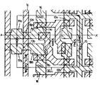
제 1 도는 CMOS 정적(static)RAM의 메모리셀(memory cell)의 평면도.1 is a plan view of a memory cell of a CMOS static RAM.
제 2 도는 제 1 도의 A-A'단면도.2 is a cross-sectional view taken along line AA ′ of FIG. 1.
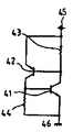
제 3 도는 종래의 CMOS정적 RAM의 구조도.3 is a structural diagram of a conventional CMOS static RAM.
제 4 도는 제 3 도의 등가회로도.4 is an equivalent circuit diagram of FIG.
제 5 도는 본 발명의 한 실시예에 따른 반도체장치의 구조도.5 is a structural diagram of a semiconductor device according to one embodiment of the present invention.
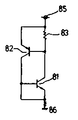
제 6 도는 제 5 도의 등가회로도.6 is an equivalent circuit diagram of FIG.
제 7 도는 본 발명의 다른 실시예에 의한 반도체장치의 구조도.7 is a structural diagram of a semiconductor device according to another embodiment of the present invention.
제 8 도는 제 7 도의 등가회로도다.8 is an equivalent circuit diagram of FIG.
* 도면의 주요부분에 대한 부호의 설명* Explanation of symbols for main parts of the drawings
도면중 51은 P형기판, 52는 n형 웰(wel1), 53은 제 1 도의 PMOS트랜지스터(12a)(12b)의 소오스, 드레인(source, drain) 영역, 전원(15)을 구성하는 P+확산영 역, 54b는 NHOS트랜지스터 (11a) (11b) 의 소오스, 드레인영역, 54a는 N웰에 접촉하기위한 영역이 되는 N+확산영역, 55a, 55b, 55c, 55d는 분리산화막, 56a, 56b, 56 c는 전원선, 접지선 또는 신호선이 되는 알루미늄등의 금속 배선층, 61은 52, 51, 54b로 이루어진 NPN트랜지스터, 52는 53, 52, 51로 이루어진 PNP트랜지스터, 63은 N웰내의 기생저항,64는 가판내의 기생저항, 65는 전원단자 66은 접지단자다.51 is a P-type substrate, 52 is an n-type well wel1, 53 is a P + diffusion constituting a source, a drain region, and a
본 발명은 상보형(相補形)금속-산화막-반도체(이하 CM0S라고 칭한다)집접회로장치의 래치업(latch-up)내량(耐量)의 개선에 관한 것이다.The present invention relates to the improvement of the latch-up resistance of a complementary metal-oxide film-semiconductor (hereinafter referred to as CM0S) integrated circuit device.
종래의 이러한 장치로서는 제 1 도-제 4 도에 보인것들이 있었다. 제 1 도는 CMOS정적 RAM(Random Access Memory)의 메모리셀의 평면도이며, 제 2 도는 제 1 도의 A-A'단면도다.Conventional such devices include those shown in FIGS. FIG. 1 is a plan view of a memory cell of a CMOS static random access memory (RAM), and FIG. 2 is a cross-sectional view taken along line A-A 'of FIG.
제 3 도는 제 1 도의 메모리셀의 전원의 공급방법을 보인 단면도이며, 제 4 도는 제 3 도의 등가회로다.3 is a cross-sectional view showing a power supply method of the memory cell of FIG. 1, and FIG. 4 is an equivalent circuit of FIG.
제 1 도의 11a, 11b는 N채널의 인버터트랜지스터, 12a, 12b는 P채널의 로드(load)트랜지스터, 13a, 13b는 판독/기록을 위한 N채널의 액세스트랜지스터, 14는 폴리실리콘으로 이루어진 워드선(word線), 15는 P+확산층으로 이루어진 전원선이며 P채널의 로드트랜지스터(12a)(12b)의 드레인에 접속되어있다.11A and 11B are N-channel inverter transistors, 12a and 12b are P-channel load transistors, 13a and 13b are N-channel access transistors for read / write, and 14 is a word line made of polysilicon. 15 is a power supply line composed of a P + diffusion layer, and is connected to the drains of the load transistors 12a and 12b of the P channel.
16은 접지(GNP), 17a, 17b는 N채널의 액세스트랜지스터(13a)(13b)의 드레인영역이며, 접촉을 통하여 도시에 없는 알루미늄으로 이루어진 비트선(bit 線)에 접속되어있다.16 is ground (GNP), and 17a and 17b are drain regions of the N-
제 2 도에서, 21은 P형기판, 22는 n형 웰(wel1)23a, 23b는 P+형 확산영역, 24a, 24b는 n+확산영역, 25a, 25b, 25c는 분리산화막, 26a, 26b, 26c는 게이트 또는 배선체가 되는 폴리실리콘, 27a, 27b는 게이트산화막이다.In FIG. 2, 21 is a P-type substrate, 22 is an n-type well 23a, 23b is a P + type diffusion region, 24a and 24b is an n + diffusion region, 25a, 25b, and 25c are separated oxide films, 26a, 26b and 26c. Is polysilicon serving as a gate or wiring, and 27a and 27b are gate oxide films.
제 3 도에 있어서, 31은 P형기판, 32는 n형 웰, 33은 제 1 도 PMOS트랜지스터(12a)(12b)의 소오스,드레인영역, 전원선(15)를 구성하는 P+확산영역, 34b는(11) 의 NMOS의 소오스드레인영역, 34a는 N웰에 접촉하기위한 영역이 되는 n+확산영역, 35a, 35b, 35c는 분리산화막, 36a, 36b는 전원선, 접지선 혹은 신호선이 되는 알루미늄등의 금속배선층이다.3, 31 is a P-type substrate, 32 is an n-type well, 33 is a source + drain region of the PMOS transistors 12a and 12b of FIG. 1, P + diffusion region constituting the
제 4 도에서, 41은 제 3 도의 (32) -(31) -(34b)로 이루어진 npn트랜지스터,42는(33) -(32) -(31)로 이루어진 pnp트랜지스터이며, 43은 n웰내의 기생저항,44는 기판내의 기생저항, 45는 전원단자, 46은 접지단자다.In FIG. 4, 41 is an np n transistor composed of (32)-(31)-(34b) in FIG. 3, 42 is a pnp transistor composed of (33)-(32)-(31), and 43 is n well. The parasitic resistance in the circuit, 44 is the parasitic resistance in the substrate, 45 is the power supply terminal, 46 is the ground terminal.
다음에 종래기술의 구성으로 이루어진 반도체장치의 동작에 관하여 설명한다.종래장치에서는 NMOS를 P형 기판내에 구성하고 PMOS를 N웰내에 구성하여 기판을 접지에, 그리고 웰을 전원에 바이어스한 상태에서 상기 NMOS, PMOS모두 정상동작을 시키고 있다. 또 N웰내의 P+영역으로 접촉홀(hole)을 통하여 외부전원(36a)또는 전원단자(45)가 직접 접속되어있다.Next, operation of a semiconductor device having a configuration of the prior art will be described. In the conventional apparatus, the NMOS is configured in the P-type substrate and the PMOS is configured in the N well, and the substrate is grounded and the well is biased to the power source. Both NMOS and PMOS are operating normally. The external power supply 36a or
종래의 반도체장치는 이상과 같이 구성되어 있으므로 N웰(32) 또는 트랜지스터(42)의 베이스에 마이너스의 전기잡음이 가해졌을때, 혹은 기판(31) 또는 트랜지스터(41)의 베이스에 플러스의 전기잡음이 가해졌을때 트랜지스터(42) 또는 (41)의 에미터-베이스 사이가 순(順)바이어스 상태가 되어 트랜지스터(42)의 도통은 트랜지스터(41)의 도통을 일으키고 트랜지스터(41)의 도통은 트랜지스터(42)의 도통을 일으키게되어 소위래치업현상을 일으키는 결접이 있었다.Since the conventional semiconductor device is configured as described above, when negative electric noise is applied to the base of the N well 32 or the
본 발명은 상기와 같이 종래의 제거하기 위하여 행해진 것으로 N웰내의 P+영역과 외부전원의 접속을, 전원에 바이어스된 N웰을 통하여 행하게 함으로써 래치업 내량이 큰 CMOS반도체 장치를 제공함을 목적으로 하고 있다. 아래에 본 발명의 한 실시예를 도면을 따라 설명한다.SUMMARY OF THE INVENTION The present invention has been made to eliminate the conventional art as described above, and an object of the present invention is to provide a CMOS semiconductor device having a large latch-up resistance by connecting a P + region in an N well with an external power source through an N well biased to a power source. have. An embodiment of the present invention is described below with reference to the drawings.
제 5 도에 있어서, 51은 P형기판, 52는 n형 웰, 53은 제 1 도의 PMOS트랜지스터(12a)(12b)의 소오스, 드레인 영역 또는 전원선(15)을 구성하는 P+확산영역, 54b는 NMOS트랜지스터(11a)또는 (11b)의 소오스,드레인영역, 54a는 N웰에 접촉하기위한 영역이 되는 n+확산영역, 55a, 55b, 55c, 55d는 분리산화막, 56a, 56b, 56c는 전원선, 접지선 또는 신호선이 되는 알루미늄등의 금속배선층이다.5, 51 is a P-type substrate, 52 is an n-type well, 53 is a P + diffusion region constituting the source, drain region, or
제 5 도의 등가회로도인 제 6 도에 있어서, 61은 ( )-(51)-(54b)로 이루어진 npn트랜지스터, 62는(53) -(52) -(51)로서 이루어진 pnp트랜지스터이며, 63은 N웰내의 기생저항, 64는 기판내의 기생저항, 65는 전원단자, 66은 접지단자다.In FIG. 6, the equivalent circuit diagram of FIG. 5, 61 is an npn transistor composed of ()-(51)-(54b), 62 is a pnp transistor composed of (53)-(52)-(51), and 63 is The parasitic resistance in the N well, 64 is the parasitic resistance in the substrate, 65 is the power supply terminal, 66 is the ground terminal.
본 발명에 의한 장치에서는 NMOS를 P기판내에 형성하고 PMOS를 N웰내에 형성하며 기판을 접지에, 그리고 웰을 전원에 바이어스한 상태에서 상기 NMOS PMOS를 동작시키는것은 종래의 장치와 마찬가지다. 종래의 장치와의 차이는 N웰내의 P+확산영역으로는 전원전압을, 전원에 바이어스된 웰내에, 상기 바이어스점(54a)과는 다른점(54c)에 n+영역을 설치하고, 이 영역(54c)에서 다른층(56c)를 경유하여 공급하고 있는 점이다.In the apparatus according to the present invention, the NMOS PMOS is formed in the P substrate, the PMOS is formed in the N well, and the NMOS PMOS is operated with the substrate biased to the ground and the well to the power supply as in the conventional apparatus. The difference from the conventional apparatus is that a P + diffusion region in an N well is provided with a power supply voltage, a n + region is provided at a
이같은 구조로 함으로써 제 6 도의 등가회로에서 보이듯이 pnp트랜지스터(62)의 에미터(53)전위는 N웰(52)내의 기생저항(63)→54c→56c경로를 거쳐서 주어지므로 (54c)와 같은 전위의 베이스(52)보다도 항상 낮다. 따라서 이 pnp트랜지스터(62)의 에미터(53), 베이스(52)가 순 바이어스되는 일은 없으며 npn, pnp의 양트랜지스터(61)(62)가 온(on)되지 않으므로 래치업현상은 일어날 수가 없다. 즉 웰으로의 전원공급부(54a)와 웰로부터의 전원인 출구(54c)를 웰내에 있어서 양단이 되도록 설치하면, 상기 pnp에미터(53), 베이스(52)가 순 바이어스되는 일은 전혀 없게되고 래치업현상은 발생할 수가 없다. 또 상기 실시예에서는 P기판을 사용한 N웰 구조의 것을 보였는데, 제 7 도와 같이 n기판을 사용한 P웰 구조의 것에 관하여 전원선 대신 접지선에 대하여 같은 방법을 사용하면 같은 효과를 나타낸다.With such a structure, as shown in the equivalent circuit of FIG. 6, the
제 7 도에서, 71은 n형의 기판, 72는 P형 웰, 73은 제 1 도의 NMOS트랜지스터(11a)(11b)의 소오스, 드레인영역, 접지(16)를 구성한 N+확산영역, 74a는 PMOS트랜지스터(12a)(12b)의 소오스, 드레인영역, 74b는 P웰에 접촉하기 위한 영역이 되는 P+확산영역, 75a, 75b, 75c, 75d는 분리산화막, 76a, 76b, 76c는 전원선, 접지선, 신호선이 되는 알루미늄 등의 금속배선층이다.In FIG. 7, 71 is an n-type substrate, 72 is a P-type well, 73 is an N + diffusion region constituting the source, drain region, and
제 8 도는 제 7 도의 등가회로도다. 이 경우 npn트랜지스터(81)의 에미터전위가 베이스전위보다도 반드시 높으므로 npn트랜지스터(81)가 도통하는 일은 없으며, 래치업이 일어날 수가 없다. 또 본 발명의 실시예에서는 전원 또는 접지에 저항이 삽입되어 회로소자의 속도성능의 열화를 초래하는 일이 있으나 CMOS RAM의 메모리셀의 전원, 접지등 소비전력이 아주 작은 부분에 적용하면 전체의 속도성능을 전혀 손상하는일 없이 래치업내량을 향상시킬수가 있다.8 is an equivalent circuit diagram of FIG. In this case, since the emitter potential of the
위와 같이 본 발명에 의하면 N웰내의 전원 또는 P웰내의 접지에로 웰을 거쳐서 급전하도록 구성한 것이므로 래치업으로 방지할 수가 있고, 신뢰성이 높은 CMOS집적회로장치를 얻을 수 있는 효과가 있다.As described above, according to the present invention, since the power is supplied to the power supply in the N well or the ground in the P well through the well, the latch can be prevented by the latch-up and the CMOS integrated circuit device with high reliability can be obtained.
Claims (4)
Applications Claiming Priority (3)
| Application Number | Priority Date | Filing Date | Title |
|---|---|---|---|
| JP59-86875 | 1984-04-28 | ||
| JP59086875A JPS60231356A (en) | 1984-04-28 | 1984-04-28 | Complementary type metal-oxide-film semiconductor integrated circuit device |
| JP86875 | 1984-04-28 |
Publications (2)
| Publication Number | Publication Date |
|---|---|
| KR850007315A KR850007315A (en) | 1985-12-02 |
| KR900003940B1 true KR900003940B1 (en) | 1990-06-04 |
Family
ID=13898998
Family Applications (1)
| Application Number | Title | Priority Date | Filing Date |
|---|---|---|---|
| KR1019850001644A KR900003940B1 (en) | 1984-04-28 | 1985-03-14 | Complementary mos ic device |
Country Status (4)
| Country | Link |
|---|---|
| US (1) | US4772930A (en) |
| JP (1) | JPS60231356A (en) |
| KR (1) | KR900003940B1 (en) |
| GB (1) | GB2158640B (en) |
Families Citing this family (5)
| Publication number | Priority date | Publication date | Assignee | Title |
|---|---|---|---|---|
| JPS60231356A (en) * | 1984-04-28 | 1985-11-16 | Mitsubishi Electric Corp | Complementary type metal-oxide-film semiconductor integrated circuit device |
| JPS648659A (en) * | 1987-06-30 | 1989-01-12 | Mitsubishi Electric Corp | Supplementary semiconductor integrated circuit device |
| US4866567A (en) * | 1989-01-06 | 1989-09-12 | Ncr Corporation | High frequency integrated circuit channel capacitor |
| US6563730B1 (en) | 2002-04-09 | 2003-05-13 | National Semiconductor Corporation | Low power static RAM architecture |
| US6711051B1 (en) | 2002-09-05 | 2004-03-23 | National Semiconductor Corporation | Static RAM architecture with bit line partitioning |
Family Cites Families (16)
| Publication number | Priority date | Publication date | Assignee | Title |
|---|---|---|---|---|
| JPS4836598B1 (en) * | 1969-09-05 | 1973-11-06 | ||
| JPS5534582B2 (en) * | 1974-06-24 | 1980-09-08 | ||
| US4006491A (en) * | 1975-05-15 | 1977-02-01 | Motorola, Inc. | Integrated circuit having internal main supply voltage regulator |
| GB1558502A (en) * | 1975-07-18 | 1980-01-03 | Tokyo Shibaura Electric Co | Semiconductor integrated circuit device |
| GB1559581A (en) * | 1975-07-18 | 1980-01-23 | Tokyo Shibaura Electric Co | Complementary mosfet device |
| JPS5234680A (en) * | 1975-09-12 | 1977-03-16 | Toshiba Corp | Integrated circuit |
| US4035826A (en) * | 1976-02-23 | 1977-07-12 | Rca Corporation | Reduction of parasitic bipolar effects in integrated circuits employing insulated gate field effect transistors via the use of low resistance substrate contacts extending through source region |
| US4100561A (en) * | 1976-05-24 | 1978-07-11 | Rca Corp. | Protective circuit for MOS devices |
| US4063274A (en) * | 1976-12-10 | 1977-12-13 | Rca Corporation | Integrated circuit device including both N-channel and P-channel insulated gate field effect transistors |
| FR2408914A1 (en) * | 1977-11-14 | 1979-06-08 | Radiotechnique Compelec | MONOLITHIC SEMICONDUCTOR DEVICE INCLUDING TWO COMPLEMENTARY TRANSISTORS AND ITS MANUFACTURING PROCESS |
| JPS5939904B2 (en) * | 1978-09-28 | 1984-09-27 | 株式会社東芝 | semiconductor equipment |
| EP0084000A3 (en) * | 1982-01-11 | 1985-07-10 | FAIRCHILD CAMERA & INSTRUMENT CORPORATION | Cmos device |
| JPS58127348A (en) * | 1982-01-25 | 1983-07-29 | Mitsubishi Electric Corp | Large scale semiconductor integrated circuit device |
| JPS60152055A (en) * | 1984-01-20 | 1985-08-10 | Matsushita Electric Ind Co Ltd | Semiconductor device |
| JPS60231356A (en) * | 1984-04-28 | 1985-11-16 | Mitsubishi Electric Corp | Complementary type metal-oxide-film semiconductor integrated circuit device |
| JPS6136946A (en) * | 1984-07-30 | 1986-02-21 | Nec Corp | Semiconductor device |
-
1984
- 1984-04-28 JP JP59086875A patent/JPS60231356A/en active Granted
-
1985
- 1985-03-14 KR KR1019850001644A patent/KR900003940B1/en not_active IP Right Cessation
- 1985-04-25 GB GB08510505A patent/GB2158640B/en not_active Expired
-
1987
- 1987-05-04 US US07/048,509 patent/US4772930A/en not_active Expired - Lifetime
Also Published As
| Publication number | Publication date |
|---|---|
| JPS60231356A (en) | 1985-11-16 |
| US4772930A (en) | 1988-09-20 |
| GB2158640B (en) | 1988-02-24 |
| JPH0144023B2 (en) | 1989-09-25 |
| GB8510505D0 (en) | 1985-05-30 |
| KR850007315A (en) | 1985-12-02 |
| GB2158640A (en) | 1985-11-13 |
Similar Documents
| Publication | Publication Date | Title |
|---|---|---|
| US6504186B2 (en) | Semiconductor device having a library of standard cells and method of designing the same | |
| JP2001352077A (en) | Soi field effect transistor | |
| US4893164A (en) | Complementary semiconductor device having high switching speed and latchup-free capability | |
| KR100479278B1 (en) | Semiconductor memory | |
| KR900003940B1 (en) | Complementary mos ic device | |
| JPH0833438B2 (en) | Test mode start circuit | |
| KR880004589A (en) | Complementary Integrated Circuit Arrangement with Substrate Bias Voltage Generator | |
| JPH0318347B2 (en) | ||
| JPH0653497A (en) | Semiconductor device equipped with i/o protective circuit | |
| JP3149999B2 (en) | Semiconductor input / output protection device | |
| KR940004455B1 (en) | Cmos semiconductor intrgrated circuit device | |
| US3590342A (en) | Mos integrated circuit with regions of ground potential interconnected through the semiconductor substrate | |
| US4740825A (en) | MOS semiconductor device having a low input resistance and a small drain capacitance | |
| JP2508968B2 (en) | Semiconductor device | |
| JP2953213B2 (en) | CMOS integrated circuit | |
| JP3088203B2 (en) | Semiconductor device | |
| JP4787554B2 (en) | I / O circuit device | |
| JPH0412627B2 (en) | ||
| JPS62211945A (en) | Semiconductor device | |
| JP3038744B2 (en) | CMOS type semiconductor integrated circuit device | |
| JPH0427159A (en) | Semiconductor device | |
| JP2555884B2 (en) | Semiconductor device operating method and semiconductor device | |
| JPS6146988B2 (en) | ||
| JPS6120147B2 (en) | ||
| KR950010050B1 (en) | Semiconductor well guard ring method |
Legal Events
| Date | Code | Title | Description |
|---|---|---|---|
| A201 | Request for examination | ||
| E902 | Notification of reason for refusal | ||
| E902 | Notification of reason for refusal | ||
| G160 | Decision to publish patent application | ||
| E701 | Decision to grant or registration of patent right | ||
| GRNT | Written decision to grant | ||
| FPAY | Annual fee payment |
Payment date: 20040524 Year of fee payment: 15 |
|
| EXPY | Expiration of term |