KR20240017841A - Roughened copper foil, copper clad laminate and printed wiring board - Google Patents
Roughened copper foil, copper clad laminate and printed wiring board Download PDFInfo
- Publication number
- KR20240017841A KR20240017841A KR1020237043495A KR20237043495A KR20240017841A KR 20240017841 A KR20240017841 A KR 20240017841A KR 1020237043495 A KR1020237043495 A KR 1020237043495A KR 20237043495 A KR20237043495 A KR 20237043495A KR 20240017841 A KR20240017841 A KR 20240017841A
- Authority
- KR
- South Korea
- Prior art keywords
- copper foil
- roughened
- cutoff
- less
- value
- Prior art date
- Legal status (The legal status is an assumption and is not a legal conclusion. Google has not performed a legal analysis and makes no representation as to the accuracy of the status listed.)
- Pending
Links
Images


Classifications
-
- C—CHEMISTRY; METALLURGY
- C25—ELECTROLYTIC OR ELECTROPHORETIC PROCESSES; APPARATUS THEREFOR
- C25D—PROCESSES FOR THE ELECTROLYTIC OR ELECTROPHORETIC PRODUCTION OF COATINGS; ELECTROFORMING; APPARATUS THEREFOR
- C25D7/00—Electroplating characterised by the article coated
- C25D7/06—Wires; Strips; Foils
- C25D7/0614—Strips or foils
-
- B—PERFORMING OPERATIONS; TRANSPORTING
- B32—LAYERED PRODUCTS
- B32B—LAYERED PRODUCTS, i.e. PRODUCTS BUILT-UP OF STRATA OF FLAT OR NON-FLAT, e.g. CELLULAR OR HONEYCOMB, FORM
- B32B15/00—Layered products comprising a layer of metal
- B32B15/04—Layered products comprising a layer of metal comprising metal as the main or only constituent of a layer, which is next to another layer of the same or of a different material
-
- B—PERFORMING OPERATIONS; TRANSPORTING
- B32—LAYERED PRODUCTS
- B32B—LAYERED PRODUCTS, i.e. PRODUCTS BUILT-UP OF STRATA OF FLAT OR NON-FLAT, e.g. CELLULAR OR HONEYCOMB, FORM
- B32B15/00—Layered products comprising a layer of metal
- B32B15/20—Layered products comprising a layer of metal comprising aluminium or copper
-
- C—CHEMISTRY; METALLURGY
- C23—COATING METALLIC MATERIAL; COATING MATERIAL WITH METALLIC MATERIAL; CHEMICAL SURFACE TREATMENT; DIFFUSION TREATMENT OF METALLIC MATERIAL; COATING BY VACUUM EVAPORATION, BY SPUTTERING, BY ION IMPLANTATION OR BY CHEMICAL VAPOUR DEPOSITION, IN GENERAL; INHIBITING CORROSION OF METALLIC MATERIAL OR INCRUSTATION IN GENERAL
- C23C—COATING METALLIC MATERIAL; COATING MATERIAL WITH METALLIC MATERIAL; SURFACE TREATMENT OF METALLIC MATERIAL BY DIFFUSION INTO THE SURFACE, BY CHEMICAL CONVERSION OR SUBSTITUTION; COATING BY VACUUM EVAPORATION, BY SPUTTERING, BY ION IMPLANTATION OR BY CHEMICAL VAPOUR DEPOSITION, IN GENERAL
- C23C26/00—Coating not provided for in groups C23C2/00 - C23C24/00
-
- C—CHEMISTRY; METALLURGY
- C25—ELECTROLYTIC OR ELECTROPHORETIC PROCESSES; APPARATUS THEREFOR
- C25D—PROCESSES FOR THE ELECTROLYTIC OR ELECTROPHORETIC PRODUCTION OF COATINGS; ELECTROFORMING; APPARATUS THEREFOR
- C25D1/00—Electroforming
- C25D1/04—Wires; Strips; Foils
-
- C—CHEMISTRY; METALLURGY
- C25—ELECTROLYTIC OR ELECTROPHORETIC PROCESSES; APPARATUS THEREFOR
- C25D—PROCESSES FOR THE ELECTROLYTIC OR ELECTROPHORETIC PRODUCTION OF COATINGS; ELECTROFORMING; APPARATUS THEREFOR
- C25D5/00—Electroplating characterised by the process; Pretreatment or after-treatment of workpieces
- C25D5/16—Electroplating with layers of varying thickness
-
- C—CHEMISTRY; METALLURGY
- C25—ELECTROLYTIC OR ELECTROPHORETIC PROCESSES; APPARATUS THEREFOR
- C25D—PROCESSES FOR THE ELECTROLYTIC OR ELECTROPHORETIC PRODUCTION OF COATINGS; ELECTROFORMING; APPARATUS THEREFOR
- C25D7/00—Electroplating characterised by the article coated
- C25D7/06—Wires; Strips; Foils
-
- H—ELECTRICITY
- H05—ELECTRIC TECHNIQUES NOT OTHERWISE PROVIDED FOR
- H05K—PRINTED CIRCUITS; CASINGS OR CONSTRUCTIONAL DETAILS OF ELECTRIC APPARATUS; MANUFACTURE OF ASSEMBLAGES OF ELECTRICAL COMPONENTS
- H05K1/00—Printed circuits
- H05K1/02—Details
- H05K1/03—Use of materials for the substrate
-
- H—ELECTRICITY
- H05—ELECTRIC TECHNIQUES NOT OTHERWISE PROVIDED FOR
- H05K—PRINTED CIRCUITS; CASINGS OR CONSTRUCTIONAL DETAILS OF ELECTRIC APPARATUS; MANUFACTURE OF ASSEMBLAGES OF ELECTRICAL COMPONENTS
- H05K1/00—Printed circuits
- H05K1/02—Details
- H05K1/09—Use of materials for the conductive, e.g. metallic pattern
Landscapes
- Chemical & Material Sciences (AREA)
- Engineering & Computer Science (AREA)
- Chemical Kinetics & Catalysis (AREA)
- Materials Engineering (AREA)
- Metallurgy (AREA)
- Organic Chemistry (AREA)
- Electrochemistry (AREA)
- Microelectronics & Electronic Packaging (AREA)
- Mechanical Engineering (AREA)
- Laminated Bodies (AREA)
- Parts Printed On Printed Circuit Boards (AREA)
Abstract
동장 적층판 내지 프린트 배선판에 사용된 경우에, 전송 특성 및 회로 직선성이 우수함과 함께, 높은 박리 강도를 실현 가능한 조화 처리 동박이 제공된다. 이 조화 처리 동박은, 적어도 한쪽의 측에 조화 처리면을 갖는다. 조화 처리면은, 조도 곡선의 첨도 Rku에 대한 조도 곡선의 절단 레벨차 Rdc의 비인 Rdc/Rku가 0.180㎛ 이하이고, 또한 파형 곡선의 최대 단면 높이 Wt가 2.50㎛ 이상 10.00㎛ 이하이다. Rku 및 Wt는, JIS B0601-2013에 준거하여 측정되는 값이고, Rdc는, JIS B0601-2013에 준거하여, 부하 길이율 20%와 부하 길이율 80% 사이에 있어서의 높이 방향의 절단 레벨 c의 차로서 얻어지는 값이다.When used in a copper clad laminate or a printed wiring board, a roughened copper foil is provided that is excellent in transmission characteristics and circuit linearity and can realize high peel strength. This roughened copper foil has a roughened surface on at least one side. For the roughened surface, Rdc/Rku, which is the ratio of the cut level difference Rdc of the roughness curve to the kurtosis Rku of the roughness curve, is 0.180 μm or less, and the maximum cross-sectional height Wt of the waveform curve is 2.50 μm or more and 10.00 μm or less. Rku and Wt are values measured based on JIS B0601-2013, and Rdc is the cutting level c in the height direction between a load length ratio of 20% and a load length ratio of 80% based on JIS B0601-2013. This is the value obtained as a car.
Description
본 발명은 조화 처리 동박, 동장 적층판 및 프린트 배선판에 관한 것이다.The present invention relates to roughened copper foil, copper clad laminate, and printed wiring board.
프린트 배선판의 제조 공정에 있어서, 동박은 절연 수지 기재와 접합된 동장 적층판의 형태로 널리 사용되고 있다. 이 점, 프린트 배선판 제조 시에 배선의 박리가 발생하는 것을 방지하기 위해, 동박과 절연 수지 기재는 높은 밀착력을 갖는 것이 요망된다. 따라서, 통상의 프린트 배선판 제조용 동박에서는, 동박의 접합면에 조화 처리를 실시하여 미세한 구리 입자로 이루어지는 요철을 형성하고, 이 요철을 프레스 가공에 의해 절연 수지 기재의 내부에 파고 들어가게 하여 앵커 효과를 발휘시킴으로써, 밀착성을 향상시키고 있다.In the manufacturing process of printed wiring boards, copper foil is widely used in the form of a copper clad laminate bonded to an insulating resin substrate. In this regard, in order to prevent peeling of wiring from occurring during the manufacture of printed wiring boards, it is desired that the copper foil and the insulating resin base material have high adhesion. Therefore, in ordinary copper foil for manufacturing printed wiring boards, the joint surface of the copper foil is roughened to form irregularities made of fine copper particles, and these irregularities are dug into the inside of the insulating resin base material by press processing to exert an anchor effect. By doing so, adhesion is improved.
이러한 조화 처리를 행한 동박으로서, 예를 들어 특허문헌 1(일본 특허 공개 제2018-172785호 공보)에는, 동박과, 동박 중 적어도 한쪽의 표면에 조화 처리층을 갖고, 조화 처리층측 표면의 산술 평균 조도 Ra가 0.08㎛ 이상 0.20㎛ 이하이고, 조화 처리층측 표면의 TD(폭 방향)의 광택도가 70% 이하인 표면 처리 동박이 개시되어 있다. 이러한 표면 처리 동박에 의하면, 동박 표면에 마련된 조화 입자의 탈락이 양호하게 억제되고, 또한 절연 기판과의 접합 시의 주름 및 줄무늬의 발생이 양호하게 억제된다고 되어 있다.As a copper foil that has undergone such a roughening treatment, for example, in Patent Document 1 (Japanese Patent Application Laid-Open No. 2018-172785), it has a roughening layer on at least one surface of the copper foil and the arithmetic mean of the surface on the roughening layer side. A surface-treated copper foil is disclosed in which the roughness Ra is 0.08 μm or more and 0.20 μm or less, and the glossiness of the TD (width direction) of the surface on the roughening layer side is 70% or less. According to this surface-treated copper foil, it is said that the falling off of the roughened particles provided on the surface of the copper foil is well suppressed, and the generation of wrinkles and stripes at the time of bonding with the insulating substrate is well suppressed.
그런데, 근년의 휴대용 전자 기기 등의 고기능화에 수반하여, 대용량 데이터의 고속 처리를 하기 위해 디지털인지 아날로그인지를 막론하고 신호의 고주파화가 진행되고 있어, 고주파 용도에 적합한 프린트 배선판이 요구되고 있다. 이러한 고주파용 프린트 배선판에는, 고주파 신호를 열화시키지 않고 전송 가능하게 하기 위해, 전송 손실의 저감이 요망된다. 프린트 배선판은 배선 패턴으로 가공된 동박과 절연 기재를 구비한 것이지만, 전송 손실에 있어서의 주된 손실로서는, 동박에 기인하는 도체 손실과, 절연 기재에 기인하는 유전 손실을 들 수 있다.However, with the recent advancement in functionality of portable electronic devices and the like, signals, whether digital or analog, are becoming higher frequency in order to process large amounts of data at high speeds, and printed wiring boards suitable for high frequency applications are in demand. In such high-frequency printed wiring boards, reduction of transmission loss is required to enable transmission of high-frequency signals without deterioration. A printed wiring board is equipped with copper foil processed into a wiring pattern and an insulating base material. The main transmission losses include conductor loss caused by the copper foil and dielectric loss caused by the insulating base material.
이 점, 전송 손실의 저감을 도모한 조화 처리 동박이 제안되어 있다. 예를 들어, 특허문헌 2(일본 특허 공개 제2015-148011호 공보)에는, 신호의 전송 손실이 작은 표면 처리 동박 및 그것을 사용한 적층판을 제공하는 것 등을 목적으로 하여, 표면 처리에 의해 동박 표면의 JIS B0601-2001에 기초하는 왜도 Rsk를 -0.35 이상 0.53 이하라고 하는 소정 범위로 제어하는 것 등이 개시되어 있다.In this regard, a roughened copper foil that aims to reduce transmission loss has been proposed. For example, Patent Document 2 (Japanese Patent Application Laid-Open No. 2015-148011) aims to provide a surface-treated copper foil with low signal transmission loss and a laminated board using the same, and the surface treatment of the copper foil is achieved by surface treatment. Controlling the skewness Rsk to a predetermined range of -0.35 or more and 0.53 or less based on JIS B0601-2001 is disclosed.
전술한 바와 같이, 근년, 프린트 배선판의 전송 특성(고주파 특성)을 향상시키는 것이 요구되고 있다. 이러한 요구에 대응하기 위해, 동박의 절연 수지 기재와의 접합면에 있어서 보다 미세한 조화 처리가 시도되고 있다. 즉, 전송 손실을 증대시키는 요인이 되는 동박 표면의 요철을 저감하기 위해, 파형이 작은 동박 표면(예를 들어 양면 평활박의 표면이나 전해 동박의 전극면)에 대하여 미세 조화 처리를 행하는 것이 생각된다. 또한, 파형이 작은 조화 처리 동박을 사용함으로써, 회로 형성 시에 있어서의 배선 패턴의 직선성(이하, 회로 직선성이라고 함)을 향상시키는 것이 생각된다. 그러나, 이러한 조화 처리 동박을 사용하여 동장 적층판의 가공 내지 프린트 배선판의 제조를 행한 경우, 대체로 동박-기재 사이의 박리 강도가 낮아, 밀착 신뢰성이 떨어진다고 하는 문제가 발생할 수 있다.As described above, in recent years, there has been a demand for improving the transmission characteristics (high frequency characteristics) of printed wiring boards. In order to meet these demands, more fine roughening treatment is being attempted on the bonding surface of copper foil with the insulating resin substrate. That is, in order to reduce the unevenness of the copper foil surface, which is a factor in increasing transmission loss, it is considered to perform micro-roughening treatment on the copper foil surface with a small waveform (for example, the surface of double-sided smooth foil or the electrode surface of electrolytic copper foil). . Furthermore, it is conceivable that the linearity (hereinafter referred to as circuit linearity) of the wiring pattern during circuit formation is improved by using roughened copper foil with a small waveform. However, when processing a copper clad laminate or manufacturing a printed wiring board using such roughened copper foil, the peeling strength between the copper foil and the base material is generally low, and a problem such as poor adhesion reliability may occur.
본 발명자들은, 금번, 조화 처리 동박의 표면에 있어서, 첨도 Rku에 대한 절단 레벨차 Rdc의 비인 Rdc/Rku, 및 최대 단면 높이 Wt를 소정의 범위로 제어함으로써, 이것을 사용하여 제조된 동장 적층판 내지 프린트 배선판에 있어서, 전송 특성 및 회로 직선성이 우수함과 함께, 높은 박리 강도를 실현할 수 있다는 지견을 얻었다.This time, the present inventors controlled Rdc/Rku, which is the ratio of the cutting level difference Rdc to kurtosis Rku, and the maximum cross-sectional height Wt to a predetermined range on the surface of the roughened copper foil, and produced a copper clad laminate or print using the same. In the wiring board, it was found that transmission characteristics and circuit linearity were excellent, and high peeling strength could be achieved.
따라서, 본 발명의 목적은, 동장 적층판 내지 프린트 배선판에 사용된 경우에, 전송 특성 및 회로 직선성이 우수함과 함께, 높은 박리 강도를 실현 가능한 조화 처리 동박을 제공하는 데 있다.Therefore, the purpose of the present invention is to provide a roughened copper foil that is excellent in transmission characteristics and circuit linearity and can realize high peel strength when used in a copper clad laminate or a printed wiring board.
본 발명에 따르면, 이하의 양태가 제공된다.According to the present invention, the following aspects are provided.
[양태 1][Mode 1]
적어도 한쪽의 측에 조화 처리면을 갖는 조화 처리 동박으로서,A roughened copper foil having a roughened surface on at least one side,
상기 조화 처리면은, 조도 곡선의 첨도 Rku에 대한 조도 곡선의 절단 레벨차 Rdc의 비인 Rdc/Rku가 0.180㎛ 이하이고, 또한 파형 곡선의 최대 단면 높이 Wt가 2.50㎛ 이상 10.00㎛ 이하이고,The roughened surface has Rdc/Rku, which is the ratio of the cut level difference Rdc of the roughness curve to the kurtosis Rku of the roughness curve, of 0.180 μm or less, and the maximum cross-sectional height Wt of the waveform curve is 2.50 μm or more and 10.00 μm or less,
상기 Rku는, JIS B0601-2013에 준거하여, 배율 200배, 컷오프값 λs에 의한 컷오프 파장 0.3㎛, 및 컷오프값 λc에 의한 컷오프 파장 5㎛의 조건에서 측정되는 값이고,The Rku is a value measured in accordance with JIS B0601-2013 under the conditions of a magnification of 200 times, a cutoff wavelength of 0.3 μm by the cutoff value λs, and a cutoff wavelength of 5 μm by the cutoff value λc,
상기 Rdc는, JIS B0601-2013에 준거하여, 배율 200배, 컷오프값 λs에 의한 컷오프 파장 0.3㎛, 및 컷오프값 λc에 의한 컷오프 파장 5㎛의 조건에서 측정되는 조도 곡선에 있어서의, 부하 길이율(Rmr1) 20%와 부하 길이율(Rmr2) 80% 사이에 있어서의 높이 방향의 절단 레벨 c의 차(c(Rmr1)-c(Rmr2))로서 얻어지는 값이고,The above Rdc is the load length ratio in the illuminance curve measured under the conditions of a magnification of 200 times, a cutoff wavelength of 0.3 μm by the cutoff value λs, and a cutoff wavelength of 5 μm by the cutoff value λc, based on JIS B0601-2013. (Rmr1) is a value obtained as the difference (c(Rmr1)-c(Rmr2)) of the cutting level c in the height direction between 20% and the load length ratio (Rmr2) 80%,
상기 Wt는, JIS B0601-2013에 준거하여, 배율 20배, 컷오프값 λc에 의한 컷오프 파장 5㎛, 및 컷오프값 λf에 의한 컷오프를 행하지 않는 조건에서 측정되는 값인, 조화 처리 동박.The Wt is a value measured in accordance with JIS B0601-2013 under conditions of a magnification of 20 times, a cutoff wavelength of 5 μm by the cutoff value λc, and no cutoff by the cutoff value λf. The roughened copper foil is a value measured.
[양태 2][Aspect 2]
상기 조화 처리면은, 상기 최대 단면 높이 Wt가 2.90㎛ 이상 10.00㎛ 이하인, 양태 1에 기재된 조화 처리 동박.The roughened copper foil according to
[양태 3][Aspect 3]
상기 조화 처리면은, 상기 절단 레벨차 Rdc가 0.45㎛ 이하인, 양태 1 또는 2에 기재된 조화 처리 동박.The roughening-treated surface is the roughening-treated copper foil according to
[양태 4][Aspect 4]
상기 조화 처리면은, 파형 곡선의 최대 산 높이 Wp가 1.00㎛ 이상 6.00㎛ 이하이고, 상기 Wp는, JIS B0601-2013에 준거하여, 배율 20배, 컷오프값 λc에 의한 컷오프 파장 5㎛, 및 컷오프값 λf에 의한 컷오프를 행하지 않는 조건에서 측정되는 값인, 양태 1 내지 3 중 어느 하나에 기재된 조화 처리 동박.The roughened surface has a maximum peak height Wp of the waveform curve of 1.00 μm or more and 6.00 μm or less, and the Wp is a magnification of 20 times, a cutoff wavelength of 5 μm by a cutoff value λc, and a cutoff value of 5 μm, based on JIS B0601-2013. The roughened copper foil according to any one of
[양태 5][Aspect 5]
상기 조화 처리면은, 조도 곡선 요소의 평균 높이 Rc가 0.70㎛ 이하이고, 상기 Rc는, JIS B0601-2013에 준거하여, 배율 200배, 컷오프값 λs에 의한 컷오프 파장 0.3㎛, 및 컷오프값 λc에 의한 컷오프 파장 5㎛의 조건에서 측정되는 값인, 양태 1 내지 4 중 어느 하나에 기재된 조화 처리 동박.In the roughened surface, the average height Rc of the roughness curve elements is 0.70 ㎛ or less, and the Rc is at a magnification of 200 times, a cutoff wavelength of 0.3 ㎛ by the cutoff value λs, and a cutoff value λc, in accordance with JIS B0601-2013. The roughened copper foil according to any one of
[양태 6][Aspect 6]
상기 조화 처리면은, 파형 곡선의 절단 레벨차 Wdc가 1.20㎛ 이상 3.10㎛ 이하이고, 상기 Wdc는, JIS B0601-2013에 준거하여, 배율 20배, 컷오프값 λc에 의한 컷오프 파장 5㎛, 및 컷오프값 λf에 의한 컷오프를 행하지 않는 조건에서 측정되는 파형 곡선에 있어서의, 부하 길이율(Wmr1) 20%와 부하 길이율(Wmr2) 80% 사이에 있어서의 높이 방향의 절단 레벨 c의 차(c(Wmr1)-c(Wmr2))로서 얻어지는 값인, 양태 1 내지 5 중 어느 하나에 기재된 조화 처리 동박.The roughened surface has a cut level difference Wdc of the waveform curve of 1.20 μm or more and 3.10 μm or less, and the Wdc is a magnification of 20 times, a cutoff wavelength of 5 μm by a cutoff value λc, and a cutoff value of 5 μm, based on JIS B0601-2013. The difference (c( The roughened copper foil according to any one of
[양태 7][Aspect 7]
상기 조화 처리면은, 조도 곡선의 제곱 평균 평방근 높이 Rq가 0.290㎛ 이하이고, 상기 Rq는, JIS B0601-2013에 준거하여, 배율 200배, 컷오프값 λs에 의한 컷오프 파장 0.3㎛, 및 컷오프값 λc에 의한 컷오프 파장 5㎛의 조건에서 측정되는 값인, 양태 1 내지 6 중 어느 하나에 기재된 조화 처리 동박.The roughened surface has a root mean square height Rq of the roughness curve of 0.290 μm or less, and Rq is based on JIS B0601-2013 at a magnification of 200 times, a cutoff wavelength of 0.3 μm by the cutoff value λs, and a cutoff value λc. The roughened copper foil according to any one of
[양태 8][Aspect 8]
상기 조화 처리면은, 상기 첨도 Rku가 1.30 이상 8.00 이하인, 양태 1 내지 7 중 어느 하나에 기재된 조화 처리 동박.The roughened copper foil according to any one of
[양태 9][Aspect 9]
상기 조화 처리면에 방청 처리층 및/또는 실란 커플링제 처리층을 구비하는, 양태 1 내지 8 중 어느 하나에 기재된 조화 처리 동박.The roughened copper foil according to any one of
[양태 10][Aspect 10]
상기 조화 처리 동박이 전해 동박이고, 상기 조화 처리면이 전해 동박의 석출면측에 존재하는, 양태 1 내지 9 중 어느 하나에 기재된 조화 처리 동박.The roughened copper foil according to any one of
[양태 11][Aspect 11]
양태 1 내지 10 중 어느 하나에 기재된 조화 처리 동박을 구비한, 동장 적층판.A copper-clad laminate provided with the roughened copper foil according to any one of
[양태 12][Aspect 12]
양태 1 내지 10 중 어느 하나에 기재된 조화 처리 동박을 구비한, 프린트 배선판.A printed wiring board provided with the roughened copper foil according to any one of
도 1은 JIS B0601-2013에 준거하여 결정되는 조도 곡선의 부하 곡선을 설명하기 위한 도면이다.
도 2는 JIS B0601-2013에 준거하여 결정되는 부하 길이율 Rmr(c)을 설명하기 위한 도면이다.
도 3은 JIS B0601-2013에 준거하여 결정되는 절단 레벨차 Rdc를 설명하기 위한 도면이다.
도 4는 조화 처리 동박의 표면 요철이, 조화 입자 성분과 파형 성분으로 이루어지는 것을 설명하기 위한 도면이다.
도 5는 본 발명의 조화 처리 동박의 일례를 도시하는 모식도이다.1 is a diagram for explaining the load curve of the roughness curve determined in accordance with JIS B0601-2013.
Figure 2 is a diagram for explaining the load length ratio Rmr(c) determined based on JIS B0601-2013.
Fig. 3 is a diagram for explaining the cutting level difference Rdc determined based on JIS B0601-2013.
FIG. 4 is a diagram for explaining that the surface irregularities of the roughened copper foil are composed of a roughened particle component and a waveform component.
Figure 5 is a schematic diagram showing an example of the roughened copper foil of the present invention.
정의Justice
본 발명을 특정하기 위해 사용되는 용어 내지 파라미터의 정의를 이하에 나타낸다.Definitions of terms and parameters used to specify the present invention are shown below.
본 명세서에 있어서 「조도 곡선의 부하 곡선」이란, 도 1에 도시되는 바와 같이, JIS B0601-2013에 준거하여 결정되는 조도 곡선을 절단 레벨 c에서 절단했을 때에 나타나는 실체부의 비율을 c의 함수로서 나타낸 곡선이다. 즉, 조도 곡선의 부하 곡선은, 부하 길이율 Rmr(c)이 0% 내지 100%가 되는 높이를 나타내는 곡선이라고도 할 수 있다. 부하 길이율 Rmr(c)이란, 도 2에 도시되는 바와 같이, JIS B0601-2013에 준거하여 결정되는 평가 길이에 대한, 절단 레벨 c에 있어서의 조도 곡선 요소의 부하 길이의 비율을 나타내는 파라미터이다.In this specification, the “load curve of the roughness curve” refers to the ratio of the solid portion that appears when the roughness curve determined based on JIS B0601-2013 is cut at the cutting level c, as shown in FIG. 1, expressed as a function of c. It's a curve. In other words, the load curve of the roughness curve can also be said to be a curve representing the height at which the load length ratio Rmr(c) is 0% to 100%. As shown in FIG. 2, the load length ratio Rmr(c) is a parameter representing the ratio of the load length of the roughness curve element at the cutting level c to the evaluation length determined based on JIS B0601-2013.
본 명세서에 있어서 「조도 곡선의 절단 레벨차 Rdc」, 「절단 레벨차 Rdc」 또는 「Rdc」란, 도 3에 도시되는 바와 같이, JIS B0601-2013에 준거하여 측정되는 조도 곡선의 부하 곡선에 있어서, 2개의 부하 길이율 Rmr1 및 Rmr2(단, Rmr1<Rmr2)의 사이에 있어서의 높이 방향의 절단 레벨 c의 차(c(Rmr1)-c(Rmr2))를 나타내는 파라미터이다. 본 명세서에서는, Rmr1을 20% 및 Rmr2를 80%로 지정하여 Rdc를 산출하는 것으로 한다.In this specification, “cut level difference Rdc of roughness curve”, “cut level difference Rdc” or “Rdc” refers to the load curve of the roughness curve measured in accordance with JIS B0601-2013, as shown in FIG. 3. , is a parameter representing the difference (c(Rmr1)-c(Rmr2)) in the cutting level c in the height direction between two load length ratios Rmr1 and Rmr2 (where Rmr1<Rmr2). In this specification, Rdc is calculated by specifying Rmr1 as 20% and Rmr2 as 80%.
본 명세서에 있어서 「조도 곡선의 제곱 평균 평방근 높이 Rq」, 「제곱 평균 평방근 높이 Rq」 또는 「Rq」란, JIS B0601-2013에 준거하여 측정되는 기준 길이에 있어서, Z(x)(Z(x)는 임의의 위치 x에 있어서의 조도 곡선의 높이를 나타냄)의 제곱 평균 평방근을 나타내는 파라미터이다.In this specification, "root-mean-square height of roughness curve Rq", "root-mean-square height Rq", or "Rq" refers to the reference length measured in accordance with JIS B0601-2013, Z(x)(Z(x) ) is a parameter representing the root mean square of (representing the height of the illumination curve at an arbitrary position x).
본 명세서에 있어서 「조도 곡선의 첨도 Rku」, 「첨도 Rku」 또는 「Rku」란, JIS B0601-2013에 준거하여 측정되는 제곱 평균 평방근 높이 Rq의 4제곱에 의해 무차원화한 기준 길이에 있어서, Z(x)의 4제곱 평균을 나타내는 파라미터이다. Rku는 표면의 뾰족함의 척도인 첨도를 의미하고, 높이 분포의 뾰족함을 나타낸다. Rku=3은 높이 분포가 정규 분포인 것을 의미하고, Rku>3이면 높이 분포가 뾰족해져 있고, Rku<3이면 높이 분포가 찌부러져 있는 형상인 것을 의미한다.In this specification, “Kurtosis Rku of the roughness curve”, “Kurtosis Rku” or “Rku” refers to the reference length non-dimensionalized by the fourth power of the root mean square height Rq measured in accordance with JIS B0601-2013, Z This parameter represents the 4-squared average of (x). Rku stands for kurtosis, a measure of the sharpness of the surface, and represents the sharpness of the height distribution. Rku=3 means that the height distribution is normal, if Rku>3 means the height distribution is sharp, and if Rku<3 means the height distribution is distorted.
본 명세서에 있어서 「Rdc/Rku」란, 첨도 Rku에 대한 절단 레벨차 Rdc의 비를 나타내는 파라미터이다.In this specification, “Rdc/Rku” is a parameter indicating the ratio of the cut level difference Rdc to the kurtosis Rku.
본 명세서에 있어서 「조도 곡선 요소의 평균 높이 Rc」, 「평균 높이 Rc」 또는 「Rc」란, JIS B0601-2013에 준거하여 측정되는 기준 길이에 있어서의 조도 곡선 요소의 높이의 평균을 나타내는 파라미터이다. 조도 곡선 요소란, 조도 곡선에 있어서의 1조의 인접하는 산 및 골을 의미한다. 조도 곡선 요소를 구성하는 산 내지 골에는, 최소 높이 및 최소 길이가 규정되어 있고, 높이가 최대 높이 Rz의 10% 이하, 혹은 길이가 기준 길이의 1% 이하인 것은 노이즈로 간주되어, 전후에 이어지는 골 내지 산의 일부가 된다.In this specification, “average height Rc of roughness curve elements”, “average height Rc” or “Rc” is a parameter representing the average height of roughness curve elements in a reference length measured in accordance with JIS B0601-2013. . A roughness curve element means a set of adjacent peaks and valleys in a roughness curve. The minimum height and minimum length are specified for the peaks and valleys that make up the roughness curve element, and those with a height of 10% or less of the maximum height Rz or a length of 1% or less of the standard length are considered noise, and the valleys that follow before and after are considered noise. It becomes part of the mountain.
본 명세서에 있어서 「파형 곡선의 최대 단면 높이 Wt」, 「최대 단면 높이 Wt」 또는 「Wt」란, JIS B0601-2013에 준거하여 측정되는 평가 길이에 있어서, 파형 곡선의 산 높이의 최댓값과 골 깊이의 최댓값의 합을 나타내는 파라미터이다.In this specification, “maximum cross-sectional height of the waveform curve Wt”, “maximum cross-sectional height Wt” or “Wt” refers to the maximum value of the peak height and trough depth of the waveform curve in the evaluation length measured in accordance with JIS B0601-2013. This is a parameter that represents the sum of the maximum values of .
본 명세서에 있어서 「파형 곡선의 최대 산 높이 Wp」, 「최대 산 높이 Wp」 또는 「Wp」란, JIS B0601-2013에 준거하여 측정되는 기준 길이에 있어서, 파형 곡선의 산 높이의 최댓값을 나타내는 파라미터이다.In this specification, “maximum peak height of the waveform curve Wp”, “maximum peak height Wp” or “Wp” refers to a parameter indicating the maximum value of the peak height of the waveform curve in the reference length measured in accordance with JIS B0601-2013. am.
본 명세서에 있어서 「파형 곡선의 부하 곡선」이란, JIS B0601-2013에 준거하여 결정되는 파형 곡선을 절단 레벨 c에서 절단했을 때에 나타나는 실체부의 비율을 c의 함수로서 나타낸 곡선이다. 즉, 파형 곡선의 부하 곡선은, 부하 길이율 Wmr(c)이 0% 내지 100%가 되는 높이를 나타내는 곡선이라고도 할 수 있다. 부하 길이율 Wmr(c)이란, JIS B0601-2013에 준거하여 결정되는 평가 길이에 대한, 절단 레벨 c에 있어서의 파형 곡선 요소의 부하 길이의 비율을 나타내는 파라미터이다.In this specification, “load curve of waveform curve” is a curve showing the ratio of the solid portion that appears when the waveform curve determined based on JIS B0601-2013 is cut at the cut level c as a function of c. In other words, the load curve of the waveform curve can also be said to be a curve representing the height at which the load length ratio Wmr(c) is 0% to 100%. The load length ratio Wmr(c) is a parameter representing the ratio of the load length of the waveform curve element at the cut level c to the evaluation length determined based on JIS B0601-2013.
본 명세서에 있어서 「파형 곡선의 절단 레벨차 Wdc」, 「절단 레벨차 Wdc」 또는 「Wdc」란, JIS B0601-2013에 준거하여 측정되는 파형 곡선의 부하 곡선에 있어서, 2개의 부하 길이율 Wmr1 및 Wmr2(단, Wmr1<Wmr2)의 사이에 있어서의 높이 방향의 절단 레벨 c의 차(c(Wmr1)-c(Wmr2))를 나타내는 파라미터이다. 본 명세서에서는, Wmr1을 20% 및 Wmr2를 80%로 지정하여 Wdc를 산출하는 것으로 한다.In this specification, “waveform curve cut level difference Wdc”, “cut level difference Wdc” or “Wdc” refers to the two load length ratios Wmr1 and This parameter represents the difference (c(Wmr1)-c(Wmr2)) in the cutting level c in the height direction between Wmr2 (where Wmr1<Wmr2). In this specification, Wdc is calculated by specifying Wmr1 as 20% and Wmr2 as 80%.
Rdc, Rq, Rku, Rc, Wt, Wp 및 Wdc는, 조화 처리면에 있어서의 소정의 측정 길이의 표면 프로파일을 시판 중인 레이저 현미경에 의해 측정함으로써 산출할 수 있다. 본 명세서에 있어서, 조도 파라미터인 Rdc, Rq, Rku 및 Rc는, 배율 200배, 컷오프값 λs에 의한 컷오프 파장 0.3㎛, 및 컷오프값 λc에 의한 컷오프 파장 5㎛의 조건에서 측정되는 것으로 한다. 또한, 조도 파라미터의 산출에 사용되는 기준 길이 및 평가 길이는, 각각 5㎛ 및 25㎛로 한다. 한편, 파형 파라미터인 Wt, Wp 및 Wdc는, 배율 20배, 컷오프값 λc에 의한 컷오프 파장 5㎛, 및 컷오프값 λf에 의한 컷오프를 행하지 않는 조건에서 측정되는 것으로 한다. 또한, 파형 파라미터의 산출에 사용되는 기준 길이 및 평가 길이는, 모두 조화 처리면의 측정 길이와 동일하게 한다. 후술하는 실시예에 있어서, 조화 처리면에 있어서의 세로 643.973㎛×가로 643.393㎛의 영역에 대하여 파형 파라미터의 측정을 행하고 있지만, 이러한 경우에 있어서의 기준 길이 및 평가 길이는, 세로 방향의 경우는 643.973㎛, 가로 방향의 경우는 643.393㎛이다. 또한, 레이저 현미경에 의한 측정에 있어서 대물 렌즈 및 광학 줌의 양쪽을 사용하는 경우, 상기 배율은 대물 렌즈의 배율에 광학 줌의 배율을 곱한 값에 상당한다. 예를 들어, 대물 렌즈 배율이 100배, 광학 줌 배율이 2배인 경우, 배율은 200배(=100×2)가 된다. 기타, 레이저 현미경에 의한 표면 프로파일의 바람직한 측정 조건 및 해석 조건에 대해서는 후술하는 실시예에 나타내는 것으로 한다.Rdc, Rq, Rku, Rc, Wt, Wp, and Wdc can be calculated by measuring the surface profile of a predetermined measurement length on the roughened surface using a commercially available laser microscope. In this specification, the illuminance parameters Rdc, Rq, Rku, and Rc are assumed to be measured under the conditions of a magnification of 200 times, a cutoff wavelength of 0.3 μm according to the cutoff value λs, and a cutoff wavelength of 5 μm according to the cutoff value λc. Additionally, the reference length and evaluation length used for calculating the roughness parameters are set to 5 μm and 25 μm, respectively. Meanwhile, the waveform parameters Wt, Wp, and Wdc are measured under the conditions of a magnification of 20 times, a cutoff wavelength of 5 μm according to the cutoff value λc, and no cutoff according to the cutoff value λf. Additionally, the reference length and evaluation length used for calculating waveform parameters are both set to be the same as the measurement length of the roughening process surface. In the examples described later, waveform parameters are measured in an area of 643.973 ㎛ in length x 643.393 ㎛ in width on the roughening surface. However, the reference length and evaluation length in this case are 643.973 in the vertical direction. ㎛, in the horizontal direction it is 643.393 ㎛. Additionally, when both an objective lens and an optical zoom are used in measurement by a laser microscope, the above magnification corresponds to the value obtained by multiplying the magnification of the objective lens by the magnification of the optical zoom. For example, if the objective lens magnification is 100x and the optical zoom magnification is 2x, the magnification is 200x (=100×2). In addition, preferred measurement conditions and analysis conditions of the surface profile by a laser microscope are shown in the Examples described later.
본 명세서에 있어서, 전해 동박의 「전극면」이란 전해 동박 제조 시에 음극과 접하고 있었던 측의 면을 가리킨다.In this specification, the “electrode surface” of the electrolytic copper foil refers to the surface on the side that was in contact with the cathode during manufacture of the electrolytic copper foil.
본 명세서에 있어서, 전해 동박의 「석출면」이란 전해 동박 제조 시에 전해 구리가 석출되어 가는 측의 면, 즉 음극과 접하고 있지 않은 측의 면을 가리킨다.In this specification, the “precipitation surface” of the electrolytic copper foil refers to the surface on the side where electrolytic copper precipitates during the manufacture of the electrolytic copper foil, that is, the surface on the side that is not in contact with the cathode.
조화 처리 동박Harmonized copper foil
본 발명의 동박은 조화 처리 동박이다. 이 조화 처리 동박은 적어도 한쪽의 측에 조화 처리면을 갖는다. 이 조화 처리면은, 조도 곡선의 첨도 Rku에 대한 조도 곡선의 절단 레벨차 Rdc의 비인 Rdc/Rku가 0.180㎛ 이하이다. 또한, 조화 처리면은, 파형 곡선의 최대 단면 높이 Wt가 2.50㎛ 이상 10.00㎛ 이하이다. 이렇게 조화 처리 동박의 표면에 있어서, Rdc/Rku, 및 최대 단면 높이 Wt를 소정의 범위로 제어함으로써, 이것을 사용하여 제조된 동장 적층판 내지 프린트 배선판에 있어서, 전송 특성(고주파 특성) 및 회로 직선성이 우수함과 함께, 높은 박리 강도를 실현할 수 있다.The copper foil of the present invention is a roughened copper foil. This roughened copper foil has a roughened surface on at least one side. For this roughened surface, Rdc/Rku, which is the ratio of the cut level difference Rdc of the roughness curve to the kurtosis Rku of the roughness curve, is 0.180 μm or less. Additionally, the roughened surface has a maximum cross-sectional height Wt of the waveform curve of 2.50 μm or more and 10.00 μm or less. In this way, on the surface of the roughened copper foil, Rdc/Rku and the maximum cross-sectional height Wt are controlled to a predetermined range, so that in the copper clad laminate or printed wiring board manufactured using this, the transmission characteristics (high frequency characteristics) and circuit linearity are improved. In addition to excellence, high peel strength can be achieved.
우수한 전송 특성 및 높은 박리 강도의 양립, 그리고 우수한 회로 직선성 및 높은 박리 강도의 양립은 본래적으로는 어려운 것이다. 이것은, 전송 특성 내지 회로 직선성을 향상시키기 위해서는, 동박 표면의 요철을 작게 하는 것이 요구되는 한편, 높은 박리 강도를 얻기 위해서는, 동박 표면의 요철을 크게 하는 것이 요구되고, 이들은 트레이드오프의 관계에 있기 때문이다. 여기서, 도 4에 도시되는 바와 같이, 조화 처리 동박 표면의 요철은 「조화 입자 성분」과, 조화 입자 성분보다 장주기의 「파형 성분」으로 이루어진다. 일반적으로, 전송 특성 내지 회로 직선성을 향상시키기 위해서는, 파형이 작은 동박 표면(예를 들어 양면 평활박의 표면이나 전해 동박의 전극면)에 대하여 미세 조화 처리를 행하여 작은 조화 입자를 형성하는 것을 생각할 수 있지만, 이러한 조화 처리 동박을 사용하여 동장 적층판 내지 프린트 배선판을 제조한 경우, 대체로 동박-기재 사이의 박리 강도가 낮아진다.It is inherently difficult to achieve both excellent transmission characteristics and high peel strength, and coexistence of excellent circuit linearity and high peel strength. This means that in order to improve the transmission characteristics or circuit linearity, it is required to reduce the irregularities on the surface of the copper foil, while in order to obtain high peel strength, it is required to increase the irregularities on the surface of the copper foil, and these are in a trade-off relationship. Because. Here, as shown in FIG. 4, the irregularities on the surface of the roughened copper foil consist of a "roughened particle component" and a "waveform component" with a longer period than the roughened particle component. Generally, in order to improve transmission characteristics or circuit linearity, it is considered to perform micro-roughening treatment on the surface of copper foil with a small waveform (for example, the surface of double-sided smooth foil or the electrode surface of electrolytic copper foil) to form small roughened particles. However, when a copper clad laminate or a printed wiring board is manufactured using such roughened copper foil, the peeling strength between the copper foil and the base material is generally lowered.
이 문제에 대하여, 본 발명자들은, 동박 표면에 있어서의 요철의 조화 입자 및 파형이 전송 특성, 회로 직선성 및 박리 강도에 미치는 영향에 대하여 검토를 행하였다. 그 결과, 동박의 파형 성분은 예상에 반하여 전송 특성에 영향을 미치기 어렵고, 주로 조화 입자의 크기가 전송 특성에 영향을 미치는 것이 판명되었다. 그리고, 본 발명자들은, 전송 특성을 양호하게 하기 위해 돌기(조화 입자)을 미세화함과 함께, 이에 의해 부족한 밀착성을 전송 특성에 대한 영향이 작은 동박의 파형에 의해 보충함으로써, 우수한 전송 특성과, 높은 박리 강도에 의한 밀착 신뢰성을 양립할 수 있는 것을 밝혀냈다. 또한, 동박의 파형을 소정의 범위 내에 제어함으로써, 우수한 회로 직선성과 높은 박리 강도를 밸런스 좋게 실현할 수 있는 것도 밝혀냈다. 구체적으로는, 절단 레벨차 Rdc를 첨도 Rku로 나눈 Rdc/Rku를 사용함으로써 전송 특성에 영향을 미치는 미소한 돌기(조화 입자)의 형상을 정확하게 반영할 수 있는 것을 지견함과 함께, Rdc/Rku를 0.180㎛ 이하로 제어함으로써, 우수한 전송 특성을 실현할 수 있는 것을 알아냈다. 또한, 최대 단면 높이 Wt가 광범위의 조화 처리면에 있어서의 파형 성분을 정확하게 반영할 수 있는 것을 지견함과 함께, 이 Wt를 2.50㎛ 이상 10.00㎛ 이하로 함으로써, 회로 직선성이 우수하면서도, 동박의 파형을 이용하여 동박-기판 사이의 높은 박리 강도를 실현할 수 있는 것도 알아냈다.Regarding this problem, the present inventors studied the influence of uneven roughened particles and waveforms on the surface of copper foil on transmission characteristics, circuit linearity, and peeling strength. As a result, contrary to expectations, it was found that the waveform component of the copper foil had little influence on the transmission characteristics, and that the size of the harmonic particles mainly affected the transmission characteristics. In order to improve the transmission characteristics, the present inventors have refined the protrusions (roughened particles) and supplemented the lack of adhesion with the waveform of the copper foil, which has little influence on the transmission characteristics, thereby achieving excellent transmission characteristics and high It was found that peel strength and adhesion reliability are compatible. Additionally, it was found that excellent circuit linearity and high peel strength can be achieved in a good balance by controlling the waveform of the copper foil within a predetermined range. Specifically, by using Rdc/Rku, which is the cutting level difference Rdc divided by the kurtosis Rku, we found that the shape of minute protrusions (harmonic particles) that affect the transmission characteristics can be accurately reflected, and Rdc/Rku It was found that excellent transmission characteristics could be realized by controlling the particle size to 0.180 μm or less. In addition, it was discovered that the maximum cross-sectional height Wt can accurately reflect the waveform component in a wide range of roughened surfaces, and by setting this Wt to 2.50 ㎛ or more and 10.00 ㎛ or less, the circuit linearity is excellent while the copper foil It was also found that high peel strength between copper foil and substrate can be achieved by using waveforms.
전송 특성, 회로 직선성 또는 박리 강도에 영향을 미치는 동박 표면의 조화 입자 성분 및 파형 성분은, 레이저 현미경에 있어서의 측정 배율, 그리고 컷오프값 λs, λc 및 λf를 구분지어 사용함으로써 구별할 수 있다. 구체적으로는, 조화 처리면을 배율 200배라고 하는 고배율로 측정함으로써, 전송 특성에 영향을 미치는 조화 처리면의 미세한 요철을 정확하게 평가할 수 있다. 그리고, 조화 처리면을 컷오프값 λs에 의한 컷오프 파장 0.3㎛, 및 컷오프값 λc에 의한 컷오프 파장 5㎛의 조건에서 측정하여 얻어지는 조도 곡선을 사용함으로써, 파형 성분의 영향이 커트된 조도 파라미터를 산출할 수 있다. 따라서, 본 발명에 있어서의 조도 파라미터, 즉 Rdc, Rku, Rdc/Rku, Rc 및 Rq는 동박 표면에 있어서의 조화 입자 성분을 적확하게 반영한 파라미터라고 할 수 있고, 이들 지표를 사용함으로써 전송 특성을 정확하게 평가할 수 있다. 이에 반해, 조화 처리면을 배율 20배라고 하는 저배율로 측정함으로써, 회로 직선성 및 밀착 신뢰성에 영향을 미치는 조화 처리면 전체의 높이(파형)를 광범위하게 평가할 수 있다. 그리고, 조화 처리면을 컷오프값 λc에 의한 컷오프 파장 5㎛, 및 컷오프값 λf에 의한 컷오프를 행하지 않는 조건에서 측정하여 얻어지는 파형 곡선을 사용함으로써, 조화 입자 성분의 영향이 커트된 파형 파라미터를 산출할 수 있다. 따라서, 본 발명에 있어서의 파형 파라미터, 즉 Wt, Wp 및 Wdc는, 동박 표면에 있어서의 파형 성분을 적확하게 반영한 파라미터라고 할 수 있고, 이들 지표를 사용함으로써 회로 직선성 및 박리 강도를 정확하게 평가할 수 있다.The harmonic particle component and waveform component of the copper foil surface that affect transmission characteristics, circuit linearity, or peel strength can be distinguished by using the measurement magnification in a laser microscope and cutoff values λs, λc, and λf. Specifically, by measuring the roughened surface at a high magnification of 200 times, the fine irregularities of the roughened surface that affect the transmission characteristics can be accurately evaluated. Then, by using the roughness curve obtained by measuring the roughened surface under the conditions of a cutoff wavelength of 0.3 μm using the cutoff value λs and a cutoff wavelength of 5 μm using the cutoff value λc, the roughness parameter with the influence of the waveform component cut out can be calculated. You can. Therefore, the roughness parameters in the present invention, namely Rdc, Rku, Rdc/Rku, Rc and Rq, can be said to be parameters that accurately reflect the roughened particle components on the copper foil surface, and by using these indices, the transmission characteristics can be accurately determined. can be evaluated. On the other hand, by measuring the roughened surface at a low magnification of 20 times, the height (waveform) of the entire roughened surface, which affects circuit linearity and adhesion reliability, can be widely evaluated. Then, by using the waveform curve obtained by measuring the roughened surface under conditions of a cutoff wavelength of 5 μm with a cutoff value λc and no cutoff with a cutoff value λf, waveform parameters in which the influence of the roughened particle component is cut can be calculated. You can. Therefore, the waveform parameters in the present invention, namely Wt, Wp, and Wdc, can be said to be parameters that accurately reflect the waveform component on the copper foil surface, and by using these indices, circuit linearity and peeling strength can be accurately evaluated. there is.
조화 처리 동박의 조화 처리면은, 파형 곡선의 최대 단면 높이 Wt가 2.50㎛ 이상 10.00㎛ 이하이고, 바람직하게는 2.90㎛ 이상 10.00㎛ 이하, 보다 바람직하게는 3.10㎛ 이상 9.00㎛ 이하, 더욱 바람직하게는 3.30㎛ 이상 7.00㎛ 이하이다. 상기 범위 내의 Wt이면, 우수한 전송 특성을 확보하면서, 우수한 회로 직선성 및 높은 박리 강도를 밸런스 좋게 실현할 수 있다.The roughened surface of the roughened copper foil has a maximum cross-sectional height Wt of the waveform curve of 2.50 ㎛ or more and 10.00 ㎛ or less, preferably 2.90 ㎛ or more and 10.00 ㎛ or less, more preferably 3.10 ㎛ or more and 9.00 ㎛ or less, even more preferably It is 3.30㎛ or more and 7.00㎛ or less. If Wt is within the above range, excellent circuit linearity and high peel strength can be achieved in a good balance while ensuring excellent transmission characteristics.
조화 처리 동박의 조화 처리면은, Rdc/Rku가 0.180㎛ 이하이고, 바람직하게는 0.015㎛ 이상 0.150㎛ 이하, 보다 바람직하게는 0.030㎛ 이상 0.110㎛ 이하, 더욱 바람직하게는 0.045㎛ 이상 0.080㎛ 이하이다. 상기 범위 내의 Rdc/Rku이면, 우수한 회로 직선성 및 높은 박리 강도이면서, 우수한 전송 특성을 실현할 수 있다.The roughened surface of the roughened copper foil has Rdc/Rku of 0.180 μm or less, preferably 0.015 μm or more and 0.150 μm or less, more preferably 0.030 μm or more and 0.110 μm or less, further preferably 0.045 μm or more and 0.080 μm or less. . If Rdc/Rku is within the above range, excellent transmission characteristics can be achieved along with excellent circuit linearity and high peel strength.
조화 처리 동박의 조화 처리면은, 조도 곡선의 절단 레벨차 Rdc가 0.45㎛ 이하인 것이 바람직하고, 보다 바람직하게는 0.04㎛ 이상 0.40㎛ 이하, 더욱 바람직하게는 0.08㎛ 이상 0.35㎛ 이하, 특히 바람직하게는 0.12㎛ 이상 0.30㎛ 이하이다. 상기 범위 내의 Rdc이면, Rdc/Rku를 상술한 범위로 제어하기 쉬워짐과 함께, 보다 한층 우수한 전송 특성을 실현할 수 있다.The roughened surface of the roughened copper foil preferably has a cut level difference Rdc of the roughness curve of 0.45 μm or less, more preferably 0.04 μm or more and 0.40 μm or less, further preferably 0.08 μm or more and 0.35 μm or less, particularly preferably It is 0.12㎛ or more and 0.30㎛ or less. If Rdc is within the above range, it becomes easy to control Rdc/Rku within the above-mentioned range, and even more excellent transmission characteristics can be realized.
조화 처리 동박의 조화 처리면은, 조도 곡선의 첨도 Rku가 1.30 이상 8.00 이하인 것이 바람직하고, 보다 바람직하게는 1.50 이상 5.50 이하, 더욱 바람직하게는 2.00 이상 4.50 이하, 특히 바람직하게는 2.50 이상 3.20 이하이다. 상기 범위 내의 Rku이면, Rdc/Rku를 상술한 범위로 제어하기 쉬워짐과 함께, 보다 한층 우수한 전송 특성을 실현할 수 있다.The roughened surface of the roughened copper foil preferably has a kurtosis Rku of 1.30 or more and 8.00 or less, more preferably 1.50 or more and 5.50 or less, further preferably 2.00 or more and 4.50 or less, particularly preferably 2.50 or more and 3.20 or less. . If Rku is within the above range, it becomes easy to control Rdc/Rku within the above-mentioned range, and even more excellent transmission characteristics can be realized.
조화 처리 동박의 조화 처리면은, 파형 곡선의 최대 산 높이 Wp가 1.00㎛ 이상 6.00㎛ 이하인 것이 바람직하고, 보다 바람직하게는 1.20㎛ 이상 5.00㎛ 이하, 더욱 바람직하게는 1.30㎛ 이상 4.30㎛ 이하, 특히 바람직하게는 1.40㎛ 이상 3.70㎛ 이하이다. 상기 범위 내의 Wp이면, 우수한 전송 특성을 확보하면서, 우수한 회로 직선성 및 높은 박리 강도를 보다 한층 밸런스 좋게 실현할 수 있다.The roughened surface of the roughened copper foil preferably has a maximum peak height Wp of the waveform curve of 1.00 μm or more and 6.00 μm or less, more preferably 1.20 μm or more and 5.00 μm or less, further preferably 1.30 μm or more and 4.30 μm or less, especially Preferably it is 1.40 ㎛ or more and 3.70 ㎛ or less. If Wp is within the above range, excellent circuit linearity and high peel strength can be achieved in a better balance while ensuring excellent transmission characteristics.
조화 처리 동박의 조화 처리면은, 조도 곡선 요소의 평균 높이 Rc가 0.70㎛ 이하인 것이 바람직하고, 보다 바람직하게는 0.06㎛ 이상 0.60㎛ 이하, 더욱 바람직하게는 0.12㎛ 이상 0.50㎛ 이하, 특히 바람직하게는 0.18㎛ 이상 0.50㎛ 이하이다. 상기 범위 내의 Rc이면, 우수한 회로 직선성 및 높은 박리 강도이면서, 보다 한층 우수한 전송 특성을 실현할 수 있다.The roughened surface of the roughened copper foil preferably has an average height Rc of the roughness curve elements of 0.70 μm or less, more preferably 0.06 μm or more and 0.60 μm or less, further preferably 0.12 μm or more and 0.50 μm or less, particularly preferably It is 0.18㎛ or more and 0.50㎛ or less. If Rc is within the above range, excellent circuit linearity and high peel strength can be achieved, and even more excellent transmission characteristics can be realized.
조화 처리 동박의 조화 처리면은, 파형 곡선의 절단 레벨차 Wdc가 1.20㎛ 이상 3.10㎛ 이하인 것이 바람직하고, 보다 바람직하게는 1.20㎛ 이상 2.70㎛ 이하, 더욱 바람직하게는 1.30㎛ 이상 2.30㎛ 이하, 특히 바람직하게는 1.60㎛ 이상 2.00㎛ 이하이다. 상기 범위 내의 Wdc이면, 우수한 전송 특성을 확보하면서, 우수한 회로 직선성 및 높은 박리 강도를 보다 한층 밸런스 좋게 실현할 수 있다.The roughened surface of the roughened copper foil preferably has a cut level difference Wdc of the waveform curve of 1.20 μm or more and 3.10 μm or less, more preferably 1.20 μm or more and 2.70 μm or less, further preferably 1.30 μm or more and 2.30 μm or less, especially Preferably it is 1.60㎛ or more and 2.00㎛ or less. If Wdc is within the above range, excellent circuit linearity and high peel strength can be realized in a better balance while ensuring excellent transmission characteristics.
조화 처리 동박의 조화 처리면은, 조도 곡선의 제곱 평균 평방근 높이 Rq가 0.290㎛ 이하인 것이 바람직하고, 보다 바람직하게는 0.030㎛ 이상 0.260㎛ 이하, 더욱 바람직하게는 0.060㎛ 이상 0.220㎛ 이하, 특히 바람직하게는 0.090㎛ 이상 0.200㎛ 이하이다. 상기 범위 내의 Rq이면, 우수한 회로 직선성 및 높은 박리 강도이면서, 보다 한층 우수한 전송 특성을 실현할 수 있다.The roughened surface of the roughened copper foil preferably has a root mean square height Rq of the roughness curve of 0.290 μm or less, more preferably 0.030 μm or more and 0.260 μm or less, further preferably 0.060 μm or more and 0.220 μm or less, particularly preferably is 0.090㎛ or more and 0.200㎛ or less. If Rq is within the above range, excellent circuit linearity and high peel strength can be achieved, and even more excellent transmission characteristics can be achieved.
조화 처리 동박의 두께는 특별히 한정되지 않지만, 0.1㎛ 이상 210㎛ 이하가 바람직하고, 보다 바람직하게는 0.3㎛ 이상 105㎛ 이하, 더욱 바람직하게는 7㎛ 이상 70㎛ 이하, 특히 바람직하게는 9㎛ 이상 35㎛ 이하이다. 또한, 본 발명의 조화 처리 동박은, 통상의 동박의 표면에 조화 처리를 행한 것에 한정되지는 않고, 캐리어를 구비한 동박의 동박 표면의 조화 처리 내지 미세 조화 처리를 행한 것이어도 된다.The thickness of the roughened copper foil is not particularly limited, but is preferably 0.1 μm or more and 210 μm or less, more preferably 0.3 μm or more and 105 μm or less, further preferably 7 μm or more and 70 μm or less, particularly preferably 9 μm or more. It is 35㎛ or less. In addition, the roughened copper foil of the present invention is not limited to that obtained by roughening the surface of a normal copper foil, and may be one in which the copper foil surface of the copper foil provided with a carrier is subjected to roughening treatment or fine roughening treatment.
본 발명의 조화 처리 동박의 일례가 도 5에 도시된다. 도 5에 도시되는 바와 같이, 본 발명의 조화 처리 동박은, 소정의 파형을 갖는 동박 표면(예를 들어 전해 동박의 석출면)에 대하여, 원하는 저조화 조건에서 조화 처리를 행하여 미세한 조화 입자를 형성함으로써, 바람직하게 제조할 수 있다. 따라서, 본 발명의 바람직한 양태에 의하면, 조화 처리 동박이 전해 동박이고, 조화 처리면이 전해 동박의 석출면측에 존재한다. 또한, 조화 처리 동박은 양측에 조화 처리면을 갖는 것이어도 되고, 한쪽의 측에만 조화 처리면을 갖는 것이어도 된다. 조화 처리면은, 전형적으로는 복수의 조화 입자를 구비하여 이루어지고, 이들 복수의 조화 입자는 각각 구리 입자로 이루어지는 것이 바람직하다. 구리 입자는 금속 구리로 이루어지는 것이어도 되고, 구리 합금으로 이루어지는 것이어도 된다.An example of the roughened copper foil of this invention is shown in FIG. 5. As shown in FIG. 5, the roughened copper foil of the present invention forms fine roughened particles by performing roughening treatment under desired low-roughening conditions on the copper foil surface (for example, the precipitation surface of electrolytic copper foil) having a predetermined waveform. By doing so, it can be manufactured preferably. Therefore, according to a preferred aspect of the present invention, the roughened copper foil is an electrolytic copper foil, and the roughened surface exists on the precipitation surface side of the electrolytic copper foil. In addition, the roughened copper foil may have a roughened surface on both sides, or may have a roughened surface only on one side. The roughened surface is typically provided with a plurality of roughened particles, and it is preferable that these plural roughened particles each consist of copper particles. The copper particles may be made of metallic copper or may be made of a copper alloy.
조화 처리면을 형성하기 위한 조화 처리는, 동박의 위에 구리 또는 구리 합금으로 조화 입자를 형성함으로써 바람직하게 행할 수 있다. 조화 처리를 행하기 전의 동박은, 무조화의 동박이어도 되고, 예비적 조화를 실시한 것이어도 된다. 조화 처리가 행해지게 되는 동박의 표면은, JIS B0601-1994에 준거하여 측정되는 10점 평균 조도 Rz가 1.30㎛ 이상 10.00㎛ 이하인 것이 바람직하고, 보다 바람직하게는 1.50㎛ 이상 8.00㎛ 이하이다. 상기 범위 내이면, 본 발명의 조화 처리 동박에 요구되는 표면 프로파일을 조화 처리면에 부여하기 쉬워진다.The roughening treatment for forming the roughening surface can be preferably performed by forming roughening particles from copper or a copper alloy on the copper foil. The copper foil before performing the roughening treatment may be unroughened copper foil, or may be one that has undergone preliminary roughening. The surface of the copper foil on which the roughening treatment is performed preferably has a 10-point average roughness Rz of 1.30 μm or more and 10.00 μm or less, as measured in accordance with JIS B0601-1994, and more preferably 1.50 μm or more and 8.00 μm or less. If it is within the above range, it becomes easy to provide the surface profile required for the roughening-treated copper foil of the present invention to the roughening-treated surface.
조화 처리는, 예를 들어 구리 농도 7g/L 이상 17g/L 이하, 황산 농도 50g/L 이상 200g/L 이하를 포함하는 황산구리 용액 중, 20℃ 이상 40℃ 이하의 온도에서, 10A/d㎡ 이상 50A/d㎡ 이하로 전해 석출을 행하는 것이 바람직하다. 이 전해 석출은 0.5초간 이상 30초간 이하 행해지는 것이 바람직하고, 1초간 이상 30초간 이하 행해지는 것이 보다 바람직하고, 1초간 이상 3초간 이하 행해지는 것이 더욱 바람직하다. 그렇지만, 본 발명에 의한 조화 처리 동박은, 상기 방법에 한정되지는 않고, 모든 방법에 의해 제조된 것이어도 된다.The roughening treatment is, for example, 10 A/dm2 or more at a temperature of 20°C or more and 40°C or less in a copper sulfate solution containing a copper concentration of 7 g/L or more and 17 g/L or less and a sulfuric acid concentration of 50 g/L or more and 200 g/L or less. It is preferable to perform electrolytic precipitation at 50 A/dm2 or less. This electrolytic deposition is preferably performed for 0.5 seconds or more and 30 seconds or less, more preferably 1 second or more and 30 seconds or less, and even more preferably performed for 1 second or more and 3 seconds or less. However, the roughened copper foil according to the present invention is not limited to the above method, and may be manufactured by any method.
상기 전해 석출 시, 하기 식:During the above electrolytic precipitation, the following formula:
(식 중, RL은 액 저항 지수(㎜ㆍL/㏖), L은 극간(양극-음극간) 거리(㎜), DC는 전하 담체 밀도(㏖/L)임)(In the formula, R L is the liquid resistance index (mm·L/mol), L is the distance between electrodes (anode-cathode) (mm), and D C is the charge carrier density (mol/L))
에 의해 정의되는 액 저항 지수 RL을 9.0㎜ㆍL/㏖ 이상 20.0㎜ㆍL/㏖ 이하로 하는 것이 바람직하고, 11.0㎜ㆍL/㏖ 이상 17.0㎜ㆍL/㏖ 이하로 하는 것이 보다 바람직하다. 이렇게 액 저항 지수 RL을 크게 함으로써 계 전체에 있어서의 전압이 커지고, 돌기 형성 반응 시의 전압도 커진다. 이것이 돌기 형상에 영향을 미치는 결과, 본 발명의 조화 처리 동박에 요구되는 표면 프로파일을 부여하는 데 적합한 형상의 돌기를 바람직하게 형성할 수 있다. 또한, 전하 담체 밀도 DC는, 도금액 중에 존재하는 모든 이온에 대해서, 각각의 이온 농도 및 가수의 곱을 합계함으로써 산출할 수 있다. 예를 들어, 도금액으로서 황산구리 용액을 사용하는 경우, 전하 담체 밀도 DC는, 하기 식:It is preferable to set the liquid resistance index R L defined by 9.0 mm·L/mol to 20.0 mm·L/mol, and more preferably to 11.0 mm·L/mol to 17.0 mm·L/mol. . By increasing the liquid resistance index R L in this way, the voltage in the entire system increases, and the voltage during the protrusion formation reaction also increases. As a result of this influencing the protrusion shape, it is possible to preferably form protrusions of a shape suitable for providing the surface profile required for the roughened copper foil of the present invention. Additionally, the charge carrier density D C can be calculated by summing the product of each ion concentration and valence for all ions present in the plating solution. For example, when using a copper sulfate solution as a plating solution, the charge carrier density D C is expressed by the following formula:
(식 중, [H+]는 용액 중의 수소 이온 농도(㏖/L), [Cu2+]는 용액 중의 구리 이온 농도(㏖/L), [SO4 2-]는 용액 중의 황산 이온 농도(㏖/L)임)(In the formula, [H + ] is the hydrogen ion concentration in the solution (mol/L), [Cu 2+ ] is the copper ion concentration in the solution (mol/L), and [SO 4 2- ] is the sulfate ion concentration in the solution (mol/L). mol/L)
에 의해 산출된다.It is calculated by
액 저항 지수 RL과 전압의 관계는 이하와 같이 설명된다. 먼저, 옴의 법칙에 의해 하기 식:The relationship between the liquid resistance index R L and voltage is explained as follows. First, according to Ohm's law, the following equation:
(식 중, V는 전압, ρ는 비저항, L은 극간 거리, I는 전류, S는 극간의 단면적임)(In the formula, V is voltage, ρ is resistivity, L is the distance between poles, I is current, and S is the cross-sectional area between poles)
이 도출된다. 즉, 전압 V는 비저항 ρ, 극간 거리 L 및 전류 밀도(=I/S)에 비례한다. 그리고, 비저항 ρ는 상술한 전하 담체 밀도 DC에 반비례한다. 이 때문에, 전류 밀도가 일정한 경우, (극간 거리 L에 비례하고, 전하 담체 밀도 DC에 반비례하는) 액 저항 지수를 크게 함으로써 전압도 커진다. 따라서, 액 저항 지수는 용액의 저항과 상관이 있는 지표라고 할 수 있다.This is derived. That is, the voltage V is proportional to the resistivity ρ, the interpole distance L, and the current density (=I/S). And, the specific resistance ρ is inversely proportional to the charge carrier density D C described above. For this reason, when the current density is constant, the voltage also increases by increasing the liquid resistance index (proportional to the interpole distance L and inversely proportional to the charge carrier density D C ). Therefore, the liquid resistance index can be said to be an index that is correlated with the resistance of the solution.
소망에 따라, 조화 처리 동박은 방청 처리가 실시되고, 방청 처리층이 형성된 것이어도 된다. 방청 처리는 아연을 사용한 도금 처리를 포함하는 것이 바람직하다. 아연을 사용한 도금 처리는 아연 도금 처리 및 아연 합금 도금 처리 중 어느 것이어도 되고, 아연 합금 도금 처리는 아연-니켈 합금 처리가 특히 바람직하다. 아연-니켈 합금 처리는 적어도 Ni 및 Zn을 포함하는 도금 처리이면 되고, Sn, Cr, Co, Mo 등의 다른 원소를 더 포함하고 있어도 된다. 예를 들어, 방청 처리층이 Ni 및 Zn에 더하여 Mo를 더 포함함으로써, 조화 처리 동박의 처리 표면이, 수지와의 밀착성, 내약품성 및 내열성이 보다 우수하고, 또한 에칭 잔사가 남기 어려운 것이 된다.Depending on desire, the roughened copper foil may be subjected to rust prevention treatment and a rust prevention treatment layer may be formed thereon. It is preferable that the rust prevention treatment includes plating treatment using zinc. The plating treatment using zinc may be either a zinc plating treatment or a zinc alloy plating treatment, and the zinc alloy plating treatment is particularly preferably a zinc-nickel alloy treatment. The zinc-nickel alloy treatment may be a plating treatment containing at least Ni and Zn, and may further contain other elements such as Sn, Cr, Co, and Mo. For example, when the rust prevention layer further contains Mo in addition to Ni and Zn, the treated surface of the roughened copper foil has better adhesion to the resin, chemical resistance, and heat resistance, and is less likely to leave an etching residue.
아연-니켈 합금 도금에 있어서의, Zn 부착량 및 Ni 부착량의 합계량에 대한 Ni 부착량의 비율인 Ni/(Zn+Ni)는 질량비로, 0.3 이상 0.9 이하가 바람직하고, 보다 바람직하게는 0.4 이상 0.9 이하, 더욱 바람직하게는 0.4 이상 0.8 이하이다. 또한, 아연-니켈 합금 도금에 있어서의 Zn 및 Ni의 합계 부착량은 8㎎/㎡ 이상 160㎎/㎡ 이하가 바람직하고, 보다 바람직하게는 13㎎/㎡ 이상 130㎎/㎡ 이하, 더욱 바람직하게는 19㎎/㎡ 이상 80㎎/㎡ 이하이다. 한편, 아연-니켈-몰리브덴 합금 도금에 있어서의, Zn 부착량, Ni 부착량 및 Mo 부착량의 합계량에 대한 Ni 부착량의 비율인 Ni/(Zn+Ni+Mo)는 질량비로, 0.20 이상 0.80 이하가 바람직하고, 보다 바람직하게는 0.25 이상 0.75 이하, 더욱 바람직하게는 0.30 이상 0.65 이하이다. 또한, 아연-니켈-몰리브덴 합금 도금에 있어서의 Zn, Ni 및 Mo의 합계 부착량은 10㎎/㎡ 이상 200㎎/㎡ 이하가 바람직하고, 보다 바람직하게는 15㎎/㎡ 이상 150㎎/㎡ 이하, 더욱 바람직하게는 20㎎/㎡ 이상 90㎎/㎡ 이하이다. Zn, Ni 및 Mo의 각 부착량은, 조화 처리 동박의 조화 처리면에 있어서의 소정의 면적(예를 들어 25㎠)을 산으로 용해하고, 얻어진 용해액 중의 각 원소 농도를 ICP 발광 분석법에 기초하여 분석함으로써 산출할 수 있다.In zinc-nickel alloy plating, Ni/(Zn+Ni), which is the ratio of the Ni adhesion amount to the total amount of the Zn adhesion amount and the Ni adhesion amount, is preferably 0.3 or more and 0.9 or less as a mass ratio, and more preferably 0.4 or more and 0.9 or less. , more preferably 0.4 or more and 0.8 or less. In addition, the total adhesion amount of Zn and Ni in zinc-nickel alloy plating is preferably 8 mg/m2 or more and 160 mg/m2 or less, more preferably 13 mg/m2 or more and 130 mg/m2 or less, and even more preferably It is more than 19㎎/㎡ and less than 80㎎/㎡. On the other hand, in zinc-nickel-molybdenum alloy plating, Ni/(Zn+Ni+Mo), which is the ratio of the Ni adhesion amount to the total amount of Zn adhesion amount, Ni adhesion amount, and Mo adhesion amount, is preferably 0.20 or more and 0.80 or less as a mass ratio. , more preferably 0.25 or more and 0.75 or less, and even more preferably 0.30 or more and 0.65 or less. In addition, the total adhesion amount of Zn, Ni, and Mo in zinc-nickel-molybdenum alloy plating is preferably 10 mg/m2 or more and 200 mg/m2 or less, more preferably 15 mg/m2 or more and 150 mg/m2 or less, More preferably, it is 20 mg/m2 or more and 90 mg/m2 or less. Each adhesion amount of Zn, Ni, and Mo is determined by dissolving a predetermined area (e.g., 25 cm 2 ) on the roughened surface of the roughened copper foil with acid, and determining the concentration of each element in the obtained solution based on ICP emission spectrometry. It can be calculated through analysis.
방청 처리는 크로메이트 처리를 더 포함하는 것이 바람직하고, 이 크로메이트 처리는 아연을 사용한 도금 처리의 후에, 아연을 포함하는 도금의 표면에 행해지는 것이 보다 바람직하다. 이렇게 함으로써 방청성을 더욱 향상시킬 수 있다. 특히 바람직한 방청 처리는, 아연-니켈 합금 도금 처리(혹은 아연-니켈-몰리브덴 합금 도금 처리)와 그 후의 크로메이트 처리의 조합이다.It is preferable that the rust prevention treatment further includes chromate treatment, and it is more preferable that this chromate treatment is performed on the surface of the plating containing zinc after the plating treatment using zinc. By doing this, rust prevention can be further improved. A particularly preferable rust prevention treatment is a combination of zinc-nickel alloy plating treatment (or zinc-nickel-molybdenum alloy plating treatment) and subsequent chromate treatment.
소망에 따라, 조화 처리 동박은 표면에 실란 커플링제 처리가 실시되어, 실란 커플링제 처리층이 형성된 것이어도 된다. 이에 의해 내습성, 내약품성 및 접착제 등과의 밀착성 등을 향상시킬 수 있다. 실란 커플링제 처리층은 실란 커플링제를 적절히 희석하여 도포하고, 건조시킴으로써 형성할 수 있다. 실란 커플링제의 예로서는, 4-글리시딜부틸트리메톡시실란, 3-글리시독시프로필트리메톡시실란 등의 에폭시 관능성 실란 커플링제, 또는 3-아미노프로필트리에톡시실란, N-(2-아미노에틸)-3-아미노프로필트리메톡시실란, N-3-(4-(3-아미노프로폭시)부톡시)프로필-3-아미노프로필트리메톡시실란, N-페닐-3-아미노프로필트리메톡시실란 등의 아미노 관능성 실란 커플링제, 또는 3-머캅토프로필트리메톡시실란 등의 머캅토 관능성 실란 커플링제, 또는 비닐트리메톡시실란, 비닐페닐트리메톡시실란 등의 올레핀 관능성 실란 커플링제, 또는 3-메타크릴옥시프로필트리메톡시실란, 3-아크릴옥시프로필트리메톡시실란 등의 아크릴 관능성 실란 커플링제, 또는 이미다졸 실란 등의 이미다졸 관능성 실란 커플링제, 또는 트리아진 실란 등의 트리아진 관능성 실란 커플링제 등을 들 수 있다.If desired, the surface of the roughened copper foil may be subjected to a silane coupling agent treatment and a silane coupling agent treatment layer may be formed. As a result, moisture resistance, chemical resistance, adhesion to adhesives, etc. can be improved. The silane coupling agent treatment layer can be formed by appropriately diluting the silane coupling agent, applying it, and drying it. Examples of silane coupling agents include epoxy functional silane coupling agents such as 4-glycidylbutyltrimethoxysilane and 3-glycidoxypropyltrimethoxysilane, or 3-aminopropyltriethoxysilane, N-(2 -Aminoethyl)-3-aminopropyltrimethoxysilane, N-3-(4-(3-aminopropoxy)butoxy)propyl-3-aminopropyltrimethoxysilane, N-phenyl-3-aminopropyl Amino-functional silane coupling agents such as trimethoxysilane, or mercapto-functional silane coupling agents such as 3-mercaptopropyltrimethoxysilane, or olefin-functional such as vinyltrimethoxysilane and vinylphenyltrimethoxysilane. A functional silane coupling agent, or an acrylic functional silane coupling agent such as 3-methacryloxypropyltrimethoxysilane or 3-acryloxypropyltrimethoxysilane, or an imidazole functional silane coupling agent such as imidazole silane, or and triazine functional silane coupling agents such as triazine silane.
상술한 이유로부터, 조화 처리 동박은 조화 처리면에 방청 처리층 및/또는 실란 커플링제 처리층을 구비하는 것이 바람직하고, 보다 바람직하게는 방청 처리층 및 실란 커플링제 처리층의 양쪽을 구비한다. 조화 처리면에 방청 처리층 및/또는 실란 커플링제 처리층이 형성되어 있는 경우, 본 명세서에 있어서의 조도 파라미터 및 파형 파라미터의 각 수치는, 방청 처리층 및/또는 실란 커플링제 처리층이 형성된 후의 조화 처리 동박의 표면을 측정하여 얻어지는 수치를 의미하는 것으로 한다. 또한, 방청 처리층 및 실란 커플링제 처리층은 조화 처리 동박의 조화 처리면측뿐만 아니라, 조화 처리면이 형성되어 있지 않은 측에 형성되어도 된다.For the above-mentioned reasons, the roughened copper foil is preferably provided with a rust-inhibiting layer and/or a silane coupling agent-treated layer on the roughened surface, and more preferably has both a rust-inhibiting layer and a silane coupling agent-treated layer. When a rust-inhibiting layer and/or a silane coupling agent-treated layer are formed on the roughened surface, the respective values of the roughness parameter and waveform parameter in this specification are the values after the rust-inhibiting layer and/or the silane coupling agent-treated layer are formed. It shall mean the numerical value obtained by measuring the surface of the roughened copper foil. In addition, the rust prevention treatment layer and the silane coupling agent treatment layer may be formed not only on the roughened surface side of the roughened copper foil but also on the side where the roughened surface is not formed.
동장 적층판Copper clad laminate
본 발명의 조화 처리 동박은 프린트 배선판용 동장 적층판의 제조에 사용되는 것이 바람직하다. 즉, 본 발명의 바람직한 양태에 의하면, 상기 조화 처리 동박을 구비한 동장 적층판이 제공된다. 본 발명의 조화 처리 동박을 사용함으로써 동장 적층판에 있어서, 우수한 전송 특성과 높은 박리 강도를 양립할 수 있다. 이 동장 적층판은, 본 발명의 조화 처리 동박과, 이 조화 처리 동박의 조화 처리면에 밀착하여 마련되는 수지층을 구비하여 이루어진다. 조화 처리 동박은 수지층의 편면에 마련되어도 되고, 양면에 마련되어도 된다. 수지층은 수지, 바람직하게는 절연성 수지를 포함하여 이루어진다. 수지층은 프리프레그 및/또는 수지 시트인 것이 바람직하다. 프리프레그란, 합성 수지판, 유리판, 유리 직포, 유리 부직포, 종이 등의 기재에 합성 수지를 함침시킨 복합 재료의 총칭이다. 절연성 수지의 바람직한 예로서는, 에폭시 수지, 시아네이트 수지, 비스말레이미드트리아진 수지(BT 수지), 폴리페닐렌에테르 수지, 페놀 수지 등을 들 수 있다. 또한, 수지 시트를 구성하는 절연성 수지의 예로서는, 에폭시 수지, 폴리이미드 수지, 폴리에스테르 수지 등의 절연 수지를 들 수 있다. 또한, 수지층에는 절연성을 향상시키는 등의 관점에서 실리카, 알루미나 등의 각종 무기 입자로 이루어지는 필러 입자 등이 함유되어 있어도 된다. 수지층의 두께는 특별히 한정되지 않지만, 1㎛ 이상 1000㎛ 이하가 바람직하고, 보다 바람직하게는 2㎛ 이상 400㎛ 이하이고, 더욱 바람직하게는 3㎛ 이상 200㎛ 이하이다. 수지층은 복수의 층으로 구성되어 있어도 된다. 프리프레그 및/또는 수지 시트 등의 수지층은 미리 동박 표면에 도포되는 프라이머 수지 층을 개재하여 조화 처리 동박에 마련되어 있어도 된다.It is preferable that the roughened copper foil of this invention is used for manufacture of a copper clad laminated board for printed wiring boards. That is, according to a preferred aspect of the present invention, a copper-clad laminated board provided with the above-mentioned roughening-treated copper foil is provided. By using the roughened copper foil of the present invention, both excellent transmission properties and high peel strength can be achieved in a copper-clad laminate. This copper-clad laminate is comprised of the roughened copper foil of this invention, and a resin layer provided in close contact with the roughened surface of this roughened copper foil. The roughened copper foil may be provided on one side of the resin layer, or may be provided on both sides. The resin layer includes a resin, preferably an insulating resin. The resin layer is preferably a prepreg and/or a resin sheet. Prepreg is a general term for composite materials made by impregnating a base material such as a synthetic resin plate, glass plate, woven glass fabric, non-woven glass fabric, or paper with a synthetic resin. Preferred examples of the insulating resin include epoxy resin, cyanate resin, bismaleimide triazine resin (BT resin), polyphenylene ether resin, and phenol resin. Additionally, examples of the insulating resin constituting the resin sheet include insulating resins such as epoxy resin, polyimide resin, and polyester resin. Additionally, the resin layer may contain filler particles made of various inorganic particles such as silica and alumina from the viewpoint of improving insulation properties, etc. The thickness of the resin layer is not particularly limited, but is preferably 1 μm or more and 1000 μm or less, more preferably 2 μm or more and 400 μm or less, and still more preferably 3 μm or more and 200 μm or less. The resin layer may be comprised of multiple layers. A resin layer such as a prepreg and/or a resin sheet may be provided in the roughened copper foil through a primer resin layer previously applied to the surface of the copper foil.
프린트 배선판printed wiring board
본 발명의 조화 처리 동박은 프린트 배선판의 제조에 사용되는 것이 바람직하다. 즉, 본 발명의 바람직한 양태에 의하면, 상기 조화 처리 동박을 구비한 프린트 배선판이 제공된다. 본 발명의 조화 처리 동박을 사용함으로써, 프린트 배선판에 있어서, 우수한 전송 특성과 높은 박리 강도를 양립할 수 있다. 본 양태에 의한 프린트 배선판은 수지층과, 구리층이 적층된 층 구성을 포함하여 이루어진다. 구리층은 본 발명의 조화 처리 동박에서 유래되는 층이다. 또한, 수지층에 대해서는 동장 적층판에 관하여 전술한 바와 같다. 어떻든간에, 프린트 배선판은 공지의 층 구성이 채용 가능하다. 프린트 배선판에 관한 구체예로서는, 프리프레그의 편면 또는 양면에 본 발명의 조화 처리 동박을 접착시켜 경화된 적층체로 한 후에 회로 형성한 편면 또는 양면 프린트 배선판이나, 이들을 다층화한 다층 프린트 배선판 등을 들 수 있다. 또한, 다른 구체예로서는, 수지 필름 위에 본 발명의 조화 처리 동박을 형성하여 회로를 형성하는 플렉시블 프린트 배선판, COF, TAB 테이프 등도 들 수 있다. 또한 다른 구체예로서는, 본 발명의 조화 처리 동박에 상술한 수지층을 도포한 수지 구비 동박(RCC)을 형성하고, 수지층을 절연 접착재층으로서 상술한 프린트 기판에 적층한 후, 조화 처리 동박을 배선층의 전부 또는 일부로 하여 모디파이드ㆍ세미ㆍ애디티브법(MSAP), 서브트랙티브법 등의 방법에 의해 회로를 형성한 빌드 업 배선판이나, 조화 처리 동박을 제거하여 세미 애디티브법(SAP)에 의해 회로를 형성한 빌드 업 배선판, 반도체 집적 회로 상에 수지 구비 동박의 적층과 회로 형성을 교호로 반복하는 다이렉트ㆍ빌드 업ㆍ온ㆍ웨이퍼 등을 들 수 있다.It is preferable that the roughened copper foil of this invention is used for manufacture of a printed wiring board. That is, according to a preferred aspect of the present invention, a printed wiring board provided with the above-mentioned roughened copper foil is provided. By using the roughened copper foil of the present invention, both excellent transmission characteristics and high peel strength can be achieved in a printed wiring board. The printed wiring board according to this aspect includes a layer structure in which a resin layer and a copper layer are laminated. The copper layer is a layer derived from the roughening-treated copper foil of the present invention. In addition, the resin layer is the same as described above with respect to the copper clad laminate. In any case, the printed wiring board can adopt a known layer configuration. Specific examples of the printed wiring board include a single-sided or double-sided printed wiring board in which the roughened copper foil of the present invention is bonded to one side or both sides of a prepreg to form a cured laminate, and then circuits are formed, and a multilayer printed wiring board obtained by multilayering these is included. . Moreover, other specific examples include a flexible printed wiring board, COF, TAB tape, etc., which form a circuit by forming the roughened copper foil of the present invention on a resin film. In another specific example, a resin-coated copper foil (RCC) is formed by applying the above-described resin layer to the roughened copper foil of the present invention, and the resin layer is laminated on the above-described printed circuit board as an insulating adhesive layer, and then the roughened copper foil is applied to the wiring layer. A build-up wiring board in which circuits are formed in whole or in part by methods such as the modified, semi-additive method (MSAP) or subtractive method, or the roughened copper foil is removed and used in the semi-additive method (SAP). Examples include direct, build-up, on-wafer, etc., which alternately repeat stacking of resin-loaded copper foil and circuit formation on a build-up wiring board on which a circuit is formed, and a semiconductor integrated circuit.
실시예Example
본 발명을 이하의 예에 의해 더욱 구체적으로 설명한다.The present invention is explained in more detail by the following examples.
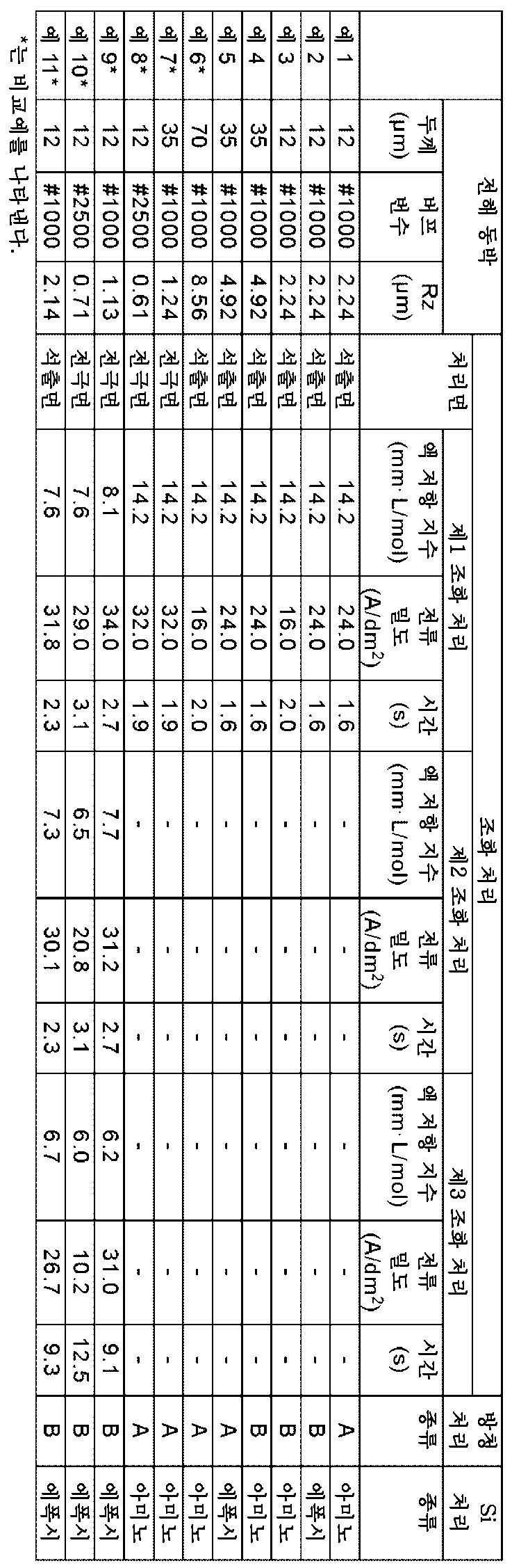
예 1 내지 11Examples 1 to 11
본 발명의 조화 처리 동박의 제조를 이하와 같이 하여 행했다.Manufacture of the roughened copper foil of this invention was performed as follows.
(1) 전해 동박의 제조(1) Manufacturing of electrolytic copper foil
구리 전해액으로서 이하에 나타내는 조성의 황산산성 황산구리 용액을 사용하고, 음극에 티타늄제의 전극을 사용하고, 양극에는 DSA(치수 안정성 양극)를 사용하여, 용액 온도 45℃, 전류 밀도 55A/d㎡로 전해하고, 표 1에 나타낸 두께의 전해 동박을 얻었다. 이때, 음극으로서, 표면을 표 1에 나타내는 번수의 버프로 연마하여 표면 조도를 조정한 전극을 사용하였다.As the copper electrolyte, an acidic copper sulfate solution with the composition shown below was used, a titanium electrode was used as the cathode, and DSA (dimensionally stable anode) was used as the anode, with a solution temperature of 45°C and a current density of 55 A/dm2. Electrolysis was performed to obtain an electrolytic copper foil with the thickness shown in Table 1. At this time, as the cathode, an electrode whose surface was polished with a buff of the number shown in Table 1 to adjust the surface roughness was used.
<황산산성 황산구리 용액의 조성><Composition of sulfuric acid copper sulfate solution>
- 구리 농도: 80g/L- Copper concentration: 80g/L
- 황산 농도: 300g/L- Sulfuric acid concentration: 300g/L
- 아교 농도: 5㎎/L- Glue concentration: 5mg/L
- 염소 농도: 30㎎/L- Chlorine concentration: 30mg/L
(2) 조화 처리(2) Harmonization processing
상술한 전해 동박이 구비하는 전극면 및 석출면 중, 예 1 내지 6 및 11에 대해서는 석출면측에 대하여, 예 7 내지 10에 대해서는 전극면측에 대하여, 조화 처리를 행하였다. 또한, 예 1 내지 6 및 11에 사용한 전해 동박의 석출면, 그리고 예 7 내지 10에 사용한 전해 동박의 전극면에 있어서의, 접촉식 표면 조도계를 사용하여 JIS B0601-1994에 준거하여 측정되는 10점 평균 조도 Rz는 표 1에 나타내는 바와 같았다.Among the electrode surfaces and precipitation surfaces provided in the above-mentioned electrolytic copper foil, roughening treatment was performed on the precipitation surface side for Examples 1 to 6 and 11, and on the electrode surface side for Examples 7 to 10. In addition, 10 points were measured in accordance with JIS B0601-1994 using a contact surface roughness meter on the deposition surface of the electrolytic copper foil used in Examples 1 to 6 and 11, and the electrode surface of the electrolytic copper foil used in Examples 7 to 10. The average illuminance Rz was as shown in Table 1.
예 1 내지 8에 대해서는, 이하에 나타내는 조화 처리(제1 조화 처리)를 행하였다. 이 조화 처리는, 조화 처리용 구리 전해 용액(구리 농도: 7g/L 이상 17g/L 이하, 황산 농도: 50g/L 이상 200g/L 이하, 액온: 30℃) 중, 각각의 예마다 표 1에 나타낸 액 저항 지수, 전류 밀도 및 시간의 조건에서 전해하고, 수세함으로써 행하였다.For Examples 1 to 8, the roughening process (first roughening process) shown below was performed. This roughening treatment is shown in Table 1 for each example in the copper electrolyte solution for roughening treatment (copper concentration: 7 g/L or more and 17 g/L or less, sulfuric acid concentration: 50 g/L or more and 200 g/L or less, liquid temperature: 30°C). Electrolysis was carried out under the conditions of the liquid resistance index, current density, and time shown, and then washed with water.
예 9 내지 11에 대해서는, 이하에 나타내는 제1 조화 처리, 제2 조화 처리 및 제3 조화 처리를 이 순서로 행하였다.For Examples 9 to 11, the first roughening process, second roughening process, and third roughening process shown below were performed in this order.
- 제1 조화 처리는, 조화 처리용 구리 전해 용액(구리 농도: 7g/L 이상 17g/L 이하, 황산 농도: 50g/L 이상 200g/L 이하, 액온: 30℃) 중, 표 1에 나타낸 액 저항 지수, 전류 밀도 및 시간의 조건에서 전해하고, 수세함으로써 행하였다.- The first roughening treatment is the solution shown in Table 1 in the copper electrolytic solution for roughening treatment (copper concentration: 7 g/L or more and 17 g/L or less, sulfuric acid concentration: 50 g/L or more and 200 g/L or less, liquid temperature: 30°C). Electrolysis was performed under the conditions of resistance index, current density, and time, and then washed with water.
- 제2 조화 처리는, 제1 조화 처리와 동일한 조성의 조화 처리용 구리 전해 용액 중, 표 1에 나타낸 액 저항 지수, 전류 밀도 및 시간의 조건에서 전해하고, 수세함으로써 행하였다.- The second roughening treatment was performed by electrolyzing in a copper electrolyte solution for roughening treatment with the same composition as the first roughening treatment under the conditions of the liquid resistance index, current density, and time shown in Table 1, and then washing with water.
- 제3 조화 처리는, 조화 처리용 구리 전해 용액(구리 농도: 65g/L 이상 80g/L 이하, 황산 농도: 50g/L 이상 200g/L 이하, 액온: 45℃) 중, 표 1에 나타낸 액 저항 지수, 전류 밀도 및 시간의 조건에서 전해하고, 수세함으로써 행하였다.- The third roughening treatment is the solution shown in Table 1 in the copper electrolyte solution for roughening treatment (copper concentration: 65 g/L or more and 80 g/L or less, sulfuric acid concentration: 50 g/L or more and 200 g/L or less, liquid temperature: 45°C). Electrolysis was performed under the conditions of resistance index, current density, and time, and then washed with water.
(3) 방청 처리(3) Rust prevention treatment
조화 처리 후의 전해 동박에 표 1에 나타낸 방청 처리를 행하였다. 이 방청 처리로서, 예 1 및 5 내지 8에 대해서는, 전해 동박의 조화 처리를 행한 면에 대해, 피로인산욕을 사용하고, 피로인산칼륨 농도 100g/L, 아연 농도 1g/L, 니켈 농도 2g/L, 몰리브덴 농도 1g/L, 액온 40℃, 전류 밀도 0.5A/d㎡로 방청 처리 A(아연-니켈-몰리브덴계 방청 처리)를 행하였다. 또한, 전해 동박의 조화 처리를 행하지 않은 면에 대해, 피로인산욕을 사용하고, 피로인산칼륨 농도 80g/L, 아연 농도 0.2g/L, 니켈 농도 2g/L, 액온 40℃, 전류 밀도 0.5A/d㎡로 방청 처리 B(아연-니켈계 방청 처리)를 행하였다. 한편, 예 2 내지 4 및 9 내지 11에 대해서는, 전해 동박의 양면에 대해, 예 1 및 5 내지 8에 있어서의 전해 동박의 조화 처리를 행하지 않은 면과 마찬가지의 조건에서 방청 처리 B를 행하였다.The rust prevention treatment shown in Table 1 was performed on the electrolytic copper foil after the roughening treatment. As this rust prevention treatment, for Examples 1 and 5 to 8, a pyrophosphate bath was used on the roughened surface of the electrolytic copper foil, and the potassium pyrophosphate concentration was 100 g/L, the zinc concentration was 1 g/L, and the nickel concentration was 2 g/L. Rust prevention treatment A (zinc-nickel-molybdenum-based rust prevention treatment) was performed at L, molybdenum concentration of 1 g/L, liquid temperature of 40°C, and current density of 0.5 A/dm2. Additionally, for the surface of the electrolytic copper foil that has not been subjected to roughening treatment, a pyrophosphate bath is used, with a potassium pyrophosphate concentration of 80 g/L, a zinc concentration of 0.2 g/L, a nickel concentration of 2 g/L, a liquid temperature of 40°C, and a current density of 0.5A. Rust prevention treatment B (zinc-nickel based rust prevention treatment) was performed at /dm2. On the other hand, for Examples 2 to 4 and 9 to 11, rust prevention treatment B was performed on both sides of the electrolytic copper foil under the same conditions as the side on which the roughening treatment of the electrolytic copper foil in Examples 1 and 5 to 8 was not performed.
(4) 크로메이트 처리(4) Chromate treatment
상기 방청 처리를 행한 전해 동박의 양면에 대하여, 크로메이트 처리를 행하고, 방청 처리층의 위에 크로메이트층을 형성하였다. 이 크로메이트 처리는 크롬산 농도 1g/L, pH 11, 액온 25℃ 및 전류 밀도 1A/d㎡의 조건에서 행하였다.Chromate treatment was performed on both sides of the electrolytic copper foil that had been subjected to the rust prevention treatment, and a chromate layer was formed on the rust prevention treatment layer. This chromate treatment was performed under the conditions of chromic acid concentration of 1 g/L, pH of 11, liquid temperature of 25°C, and current density of 1 A/dm2.
(5) 실란 커플링제 처리(5) Silane coupling agent treatment
상기 크로메이트 처리가 실시된 동박을 수세하고, 그 후 즉시 실란 커플링제 처리를 행하고, 조화 처리면의 크로메이트층 위에 실란 커플링제를 흡착시켰다. 이 실란 커플링제 처리는, 순수를 용매로 하는 실란 커플링제의 용액을 샤워링으로 조화 처리면에 분사하여 흡착 처리함으로써 행하였다. 실란 커플링제로서, 예 1, 3, 4 및 6 내지 8에서는 3-아미노프로필트리메톡시실란, 예 2, 5 및 9 내지 11에서는 3-글리시독시프로필트리메톡시실란을 사용하였다. 실란 커플링제의 농도는 모두 3g/L로 하였다. 실란 커플링제의 흡착 후, 최종적으로 전열기에 의해 수분을 증발시켜, 소정 두께의 조화 처리 동박을 얻었다.The copper foil to which the chromate treatment was given was washed with water, and then immediately treated with a silane coupling agent, and the silane coupling agent was adsorbed onto the chromate layer of the roughened surface. This silane coupling agent treatment was performed by spraying a solution of the silane coupling agent using pure water as a solvent onto the roughened surface using a shower ring and performing adsorption treatment. As a silane coupling agent, 3-aminopropyltrimethoxysilane was used in Examples 1, 3, 4, and 6 to 8, and 3-glycidoxypropyltrimethoxysilane was used in Examples 2, 5, and 9 to 11. The concentration of the silane coupling agent was all set to 3 g/L. After adsorption of the silane coupling agent, moisture was finally evaporated using a heater to obtain a roughened copper foil of a predetermined thickness.
평가evaluation
제조된 조화 처리 동박에 대해서, 이하에 나타내는 각종 평가를 행하였다.The various evaluations shown below were performed on the manufactured roughened copper foil.
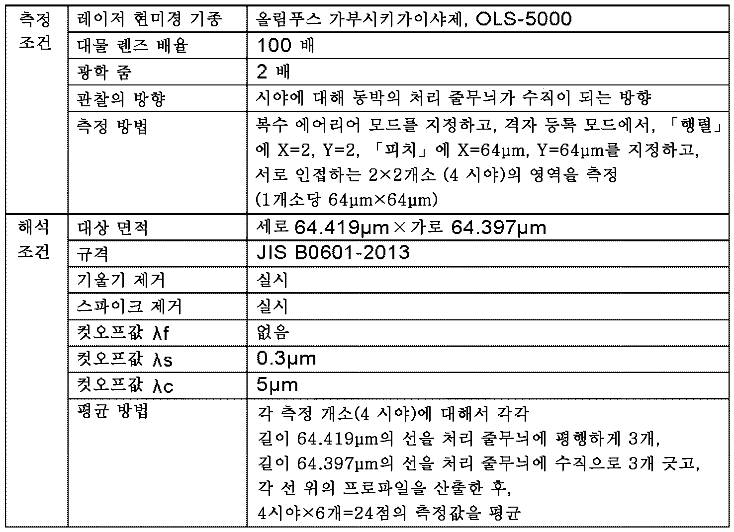
<조화 처리면의 표면 성상 파라미터><Surface property parameters of roughened surface>
레이저 현미경(올림푸스 가부시키가이샤 제조, OLS-5000)을 사용한 표면 조도 해석에 의해, 조화 처리 동박의 조화 처리면의 측정을 JIS B0601-2013에 준거하여 행했다. 이때, 조도 파라미터(Rdc, Rku, Rc 및 Rq)에 대해서는 표 2에 나타내는 바와 같이 측정 배율을 200배(대물 렌즈 배율 100배×광학 줌 2배)로 하고, 파형 파라미터(Wdc, Wt 및 Wp)에 대해서는 표 3에 나타내는 바와 같이 측정 배율을 20배(대물 렌즈 배율 20배)로 하여 측정을 행하였다. 그 밖의 구체적인 측정 조건은 표 2 및 3에 나타내는 바와 같았다. 얻어진 조화 처리면의 표면 프로파일에 대하여, 표 2 및 3에 나타내는 조건에 따라서 해석을 행하고, Rdc, Rku, Rc, Rq, Wdc, Wt 및 Wp를 산출하였다. 또한, 얻어진 Rdc 및 Rku의 값에 기초하여, Rdc/Rku를 산출하였다. 결과는 표 4에 나타내는 바와 같았다.The roughened surface of the roughened copper foil was measured by surface roughness analysis using a laser microscope (OLS-5000, manufactured by Olympus Corporation) in accordance with JIS B0601-2013. At this time, for the illuminance parameters (Rdc, Rku, Rc, and Rq), the measurement magnification is set to 200 times (100 times objective lens magnification × 2 times optical zoom) as shown in Table 2, and the waveform parameters (Wdc, Wt, and Wp) As shown in Table 3, the measurement was performed at a measurement magnification of 20 times (objective lens magnification of 20 times). Other specific measurement conditions were as shown in Tables 2 and 3. The surface profile of the obtained roughened surface was analyzed according to the conditions shown in Tables 2 and 3, and Rdc, Rku, Rc, Rq, Wdc, Wt, and Wp were calculated. Additionally, based on the obtained values of Rdc and Rku, Rdc/Rku was calculated. The results were as shown in Table 4.

<방청 처리층에 있어서의 원소 부착량의 측정><Measurement of element adhesion amount in rust prevention treatment layer>
조화 처리 동박의 조화 처리면에 있어서의 면적 25㎠(5㎝×5㎝)의 영역을 산으로 용해하고, 얻어진 용해액 중의 Zn, Ni 및 Mo의 각 농도를 ICP 발광 분석법에 의해 분석하여, Zn 부착량, Ni 부착량 및 Mo 부착량을 측정하였다. 결과는 표 4에 나타내는 바와 같았다.An area of 25 cm2 (5 cm The adhesion amount, Ni adhesion amount, and Mo adhesion amount were measured. The results were as shown in Table 4.
<동장 적층판의 제작><Production of copper clad laminate>
절연 기재로서, 폴리페닐렌에테르와 트리알릴이소시아누레이트와 비스말레이미드 수지를 주성분으로 하는 프리프레그(두께 100㎛) 2매를 준비하여, 적층하였다. 이 적층한 프리프레그에, 제조한 표면 처리 동박을 그 조화 처리면이 프리프레그와 맞닿도록 적층하고, 32kgf/㎠, 205℃에서 120분간의 프레스를 행하여, 34㎝×34㎝의 동장 적층판을 제작하였다.As an insulating substrate, two sheets of prepreg (
<회로 직선성><Circuit linearity>
회로 직선성의 평가를 다음과 같이 하여 행하였다. 먼저, 예 4 내지 7에 대해서, 동박의 두께가 12㎛가 될 때까지 상술한 동장 적층판의 동박측 표면에 대하여 에칭을 행하였다. 예 1 내지 11에 대해서, 동장 적층판의 동박측 표면에 드라이 필름을 첩부하고, 노광 및 현상을 행하고, 에칭 레지스트를 형성하였다. 염화구리 에칭액으로 처리함으로써, 레지스트 사이로부터 구리를 용해 제거하고, 회로 폭 300㎛, 회로 높이 12㎛, 길이 10㎝ 또는 15㎝의 직선상 회로를 3개씩(합계 6개) 형성하였다. 이렇게 하여 얻어진 직선상 회로를 광학 현미경으로 관찰하고, 1개의 회로당 무작위로 30개소를 선택하여 회로 폭을 측정하였다. 얻어진 30개의 회로 폭 데이터의 조에 대하여 평균값 및 표준 편차를 계산하고, 표준 편차를 평균값으로 나눔으로써, 회로마다의 변동 계수(%)를 산출하였다. 6개의 회로에 있어서의 변동 계수의 평균값을 구하고, 각 예에 있어서의 회로 폭 변동 계수로 하였다. 얻어진 회로 폭 변동 계수의 양부를 이하의 기준에 따라서 평가하였다. 결과는 표 4에 나타내는 바와 같았다.Circuit linearity was evaluated as follows. First, for Examples 4 to 7, etching was performed on the surface of the copper foil side of the copper clad laminate described above until the thickness of the copper foil reached 12 μm. For Examples 1 to 11, a dry film was affixed to the surface of the copper foil side of the copper clad laminate, exposure and development were performed, and an etching resist was formed. By treating with a copper chloride etching solution, copper was dissolved and removed from between the resists, and three linear circuits each having a circuit width of 300 μm, a circuit height of 12 μm, and a length of 10 cm or 15 cm were formed (6 in total). The linear circuit thus obtained was observed under an optical microscope, and 30 locations per circuit were randomly selected to measure the circuit width. The average value and standard deviation were calculated for the obtained set of 30 circuit width data, and the coefficient of variation (%) for each circuit was calculated by dividing the standard deviation by the average value. The average value of the coefficient of variation in the six circuits was determined and used as the coefficient of variation of the circuit width in each example. The quality of the obtained circuit width variation coefficient was evaluated according to the following criteria. The results were as shown in Table 4.
<회로 폭 변동 계수 평가 기준><Circuit width variation coefficient evaluation criteria>
- 양호: 회로 폭 변동 계수가 1.50% 이하- Good: Circuit width variation coefficient is 1.50% or less
- 불량: 회로 폭 변동 계수가 1.50% 초과- Defect: Circuit width variation coefficient exceeds 1.50%
<동박-기재 사이의 박리 강도><Peel strength between copper foil and substrate>
조화 처리 동박 및 절연 기재 사이의 밀착성을 평가하기 위해, 상태(常態) 박리 강도의 측정을 다음과 같이 하여 행하였다. 먼저, 예 4 내지 7에 대해서, 동박의 두께가 12㎛가 될 때까지 상술한 동장 적층판의 동박측 표면에 대하여 에칭을 행하였다. 예 1 내지 11에 대해서, 동장 적층판에 에칭법에 의해 회로 형성을 행하고, 3㎜ 폭의 직선 회로를 구비한 시험 기판을 제조하였다. 이렇게 하여 얻어진 직선 회로를, JIS C 5016-1994의 A법(90° 박리)에 준거하여 절연 기재로부터 박리하여 상태 박리 강도(kgf/㎝)를 측정하였다. 얻어진 상태 박리 강도의 양부를 이하의 기준에 따라서 평가하였다. 결과는 표 4에 나타내는 바와 같았다.In order to evaluate the adhesion between the roughened copper foil and the insulating substrate, the normal peel strength was measured as follows. First, for Examples 4 to 7, etching was performed on the surface of the copper foil side of the copper clad laminate described above until the thickness of the copper foil reached 12 μm. For Examples 1 to 11, circuit formation was performed on a copper clad laminate by an etching method, and a test board with a 3 mm wide straight circuit was manufactured. The linear circuit obtained in this way was peeled from the insulating substrate in accordance with method A (90° peel) of JIS C 5016-1994, and the peeling strength (kgf/cm) was measured. The quality of the obtained peeling strength was evaluated according to the following criteria. The results were as shown in Table 4.
<상태 박리 강도 평가 기준><State peel strength evaluation criteria>
- 양호: 상태 박리 강도가 0.30kgf/㎝ 이상- Good: condition peeling strength of 0.30kgf/cm or more
- 불량: 상태 박리 강도가 0.30kgf/㎝ 미만- Poor: Condition peeling strength is less than 0.30kgf/cm
(c) 전송 특성(c) Transmission characteristics
절연 수지 기재로서 고주파용 기재(파나소닉제, MEGTRON6N)를 준비하였다. 이 절연 수지 기재의 양면에 조화 처리 동박을 그 조화 처리면이 절연 수지 기재와 맞닿도록 적층하고, 진공 프레스기를 사용하여, 온도 190℃, 프레스 시간 120분의 조건에서 적층하고, 절연 두께 136㎛의 동장 적층판을 얻었다. 그 후, 당해 동장 적층판에 에칭 가공을 실시하고, 특성 임피던스가 50Ω이 되도록 마이크로 스트립 라인을 형성한 전송 손실 측정용 기판을 얻었다. 얻어진 전송 손실 측정용 기판에 대하여, 네트워크 애널라이저(키사이트 테크놀로지제, N5225B)를 사용하여, 28㎓의 전송 손실(㏈/㎝)을 측정하였다. 얻어진 전송 손실의 양부를 이하의 기준에 따라서 평가하였다. 결과는 표 4에 나타내는 바와 같았다.A high-frequency substrate (MEGTRON6N, manufactured by Panasonic) was prepared as an insulating resin substrate. Roughened copper foil was laminated on both sides of this insulating resin base material so that the roughened surface was in contact with the insulating resin base material, and was laminated using a vacuum press under conditions of a temperature of 190°C and a pressing time of 120 minutes, and an insulating thickness of 136 ㎛ was formed. A copper clad laminate was obtained. After that, etching processing was performed on the copper-clad laminate to obtain a substrate for transmission loss measurement on which microstrip lines were formed so that the characteristic impedance was 50 Ω. For the obtained substrate for transmission loss measurement, the transmission loss (dB/cm) at 28 GHz was measured using a network analyzer (N5225B, manufactured by Keysight Technologies). The quality of the obtained transmission loss was evaluated according to the following criteria. The results were as shown in Table 4.
<전송 손실 평가 기준><Transmission loss evaluation criteria>
- 양호: 전송 손실이 -0.33㏈/㎝ 이상- Good: Transmission loss is -0.33dB/cm or more
- 불량: 전송 손실이 -0.33㏈/㎝ 미만- Poor: Transmission loss is less than -0.33dB/cm
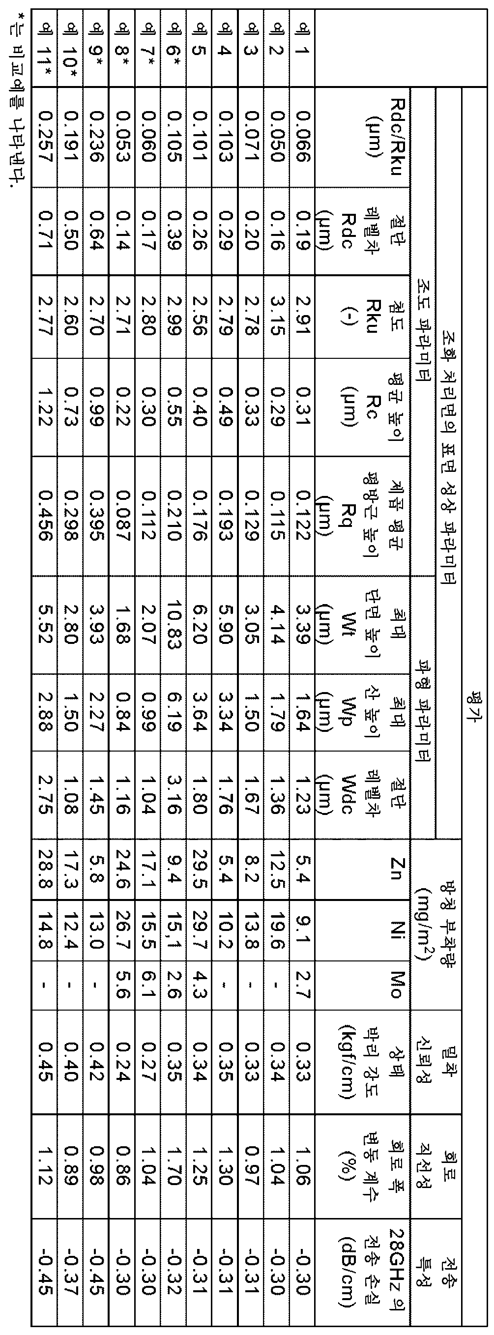
Claims (12)
상기 조화 처리면은, 조도 곡선의 첨도 Rku에 대한 조도 곡선의 절단 레벨차 Rdc의 비인 Rdc/Rku가 0.180㎛ 이하이고, 또한 파형 곡선의 최대 단면 높이 Wt가 2.50㎛ 이상 10.00㎛ 이하이고,
상기 Rku는, JIS B0601-2013에 준거하여, 배율 200배, 컷오프값 λs에 의한 컷오프 파장 0.3㎛, 및 컷오프값 λc에 의한 컷오프 파장 5㎛의 조건에서 측정되는 값이고,
상기 Rdc는, JIS B0601-2013에 준거하여, 배율 200배, 컷오프값 λs에 의한 컷오프 파장 0.3㎛, 및 컷오프값 λc에 의한 컷오프 파장 5㎛의 조건에서 측정되는 조도 곡선에 있어서의, 부하 길이율(Rmr1) 20%와 부하 길이율(Rmr2) 80% 사이에 있어서의 높이 방향의 절단 레벨 c의 차(c(Rmr1)-c(Rmr2))로서 얻어지는 값이고,
상기 Wt는, JIS B0601-2013에 준거하여, 배율 20배, 컷오프값 λc에 의한 컷오프 파장 5㎛, 및 컷오프값 λf에 의한 컷오프를 행하지 않는 조건에서 측정되는 값인, 조화 처리 동박.A roughened copper foil having a roughened surface on at least one side,
The roughened surface has Rdc/Rku, which is the ratio of the cut level difference Rdc of the roughness curve to the kurtosis Rku of the roughness curve, of 0.180 μm or less, and the maximum cross-sectional height Wt of the waveform curve is 2.50 μm or more and 10.00 μm or less,
The Rku is a value measured in accordance with JIS B0601-2013 under the conditions of a magnification of 200 times, a cutoff wavelength of 0.3 μm by the cutoff value λs, and a cutoff wavelength of 5 μm by the cutoff value λc,
The above Rdc is the load length ratio in the illuminance curve measured under the conditions of a magnification of 200 times, a cutoff wavelength of 0.3 μm by the cutoff value λs, and a cutoff wavelength of 5 μm by the cutoff value λc, based on JIS B0601-2013. (Rmr1) is a value obtained as the difference (c(Rmr1)-c(Rmr2)) of the cutting level c in the height direction between 20% and the load length ratio (Rmr2) 80%,
The Wt is a value measured in accordance with JIS B0601-2013 under conditions of a magnification of 20 times, a cutoff wavelength of 5 μm by the cutoff value λc, and no cutoff by the cutoff value λf. The roughened copper foil is a value measured.
상기 조화 처리면은, 상기 최대 단면 높이 Wt가 2.90㎛ 이상 10.00㎛ 이하인, 조화 처리 동박.According to paragraph 1,
The roughened copper foil has a maximum cross-sectional height Wt of 2.90 μm or more and 10.00 μm or less.
상기 조화 처리면은, 상기 절단 레벨차 Rdc가 0.45㎛ 이하인, 조화 처리 동박.According to claim 1 or 2,
The roughened copper foil has a cutting level difference Rdc of 0.45 μm or less.
상기 조화 처리면은, 파형 곡선의 최대 산 높이 Wp가 1.00㎛ 이상 6.00㎛ 이하이고, 상기 Wp는, JIS B0601-2013에 준거하여, 배율 20배, 컷오프값 λc에 의한 컷오프 파장 5㎛, 및 컷오프값 λf에 의한 컷오프를 행하지 않는 조건에서 측정되는 값인, 조화 처리 동박.According to claim 1 or 2,
The roughened surface has a maximum peak height Wp of the waveform curve of 1.00 μm or more and 6.00 μm or less, and the Wp is a magnification of 20 times, a cutoff wavelength of 5 μm by a cutoff value λc, and a cutoff value of 5 μm, based on JIS B0601-2013. Roughened copper foil, which is a value measured under the condition of not performing a cutoff by the value λf.
상기 조화 처리면은, 조도 곡선 요소의 평균 높이 Rc가 0.70㎛ 이하이고, 상기 Rc는, JIS B0601-2013에 준거하여, 배율 200배, 컷오프값 λs에 의한 컷오프 파장 0.3㎛, 및 컷오프값 λc에 의한 컷오프 파장 5㎛의 조건에서 측정되는 값인, 조화 처리 동박.According to claim 1 or 2,
In the roughened surface, the average height Rc of the roughness curve elements is 0.70 ㎛ or less, and the Rc is at a magnification of 200 times, a cutoff wavelength of 0.3 ㎛ by the cutoff value λs, and a cutoff value λc, in accordance with JIS B0601-2013. This value is measured under the condition of a cutoff wavelength of 5㎛, roughened copper foil.
상기 조화 처리면은, 파형 곡선의 절단 레벨차 Wdc가 1.20㎛ 이상 3.10㎛ 이하이고, 상기 Wdc는, JIS B0601-2013에 준거하여, 배율 20배, 컷오프값 λc에 의한 컷오프 파장 5㎛, 및 컷오프값 λf에 의한 컷오프를 행하지 않는 조건에서 측정되는 파형 곡선에 있어서의, 부하 길이율(Wmr1) 20%와 부하 길이율(Wmr2) 80% 사이에 있어서의 높이 방향의 절단 레벨 c의 차(c(Wmr1)-c(Wmr2))로서 얻어지는 값인, 조화 처리 동박.According to claim 1 or 2,
The roughened surface has a cut level difference Wdc of the waveform curve of 1.20 μm or more and 3.10 μm or less, and the Wdc is a magnification of 20 times, a cutoff wavelength of 5 μm by a cutoff value λc, and a cutoff value of 5 μm, based on JIS B0601-2013. The difference (c( Roughened copper foil whose value is obtained as Wmr1)-c(Wmr2)).
상기 조화 처리면은, 조도 곡선의 제곱 평균 평방근 높이 Rq가 0.290㎛ 이하이고, 상기 Rq는, JIS B0601-2013에 준거하여, 배율 200배, 컷오프값 λs에 의한 컷오프 파장 0.3㎛, 및 컷오프값 λc에 의한 컷오프 파장 5㎛의 조건에서 측정되는 값인, 조화 처리 동박.According to claim 1 or 2,
The roughened surface has a root mean square height Rq of the roughness curve of 0.290 μm or less, and Rq is based on JIS B0601-2013 at a magnification of 200 times, a cutoff wavelength of 0.3 μm by the cutoff value λs, and a cutoff value λc. The roughened copper foil is a value measured under the condition of a cutoff wavelength of 5㎛.
상기 조화 처리면은, 상기 첨도 Rku가 1.30 이상 8.00 이하인, 조화 처리 동박.According to claim 1 or 2,
The roughened surface is a roughened copper foil whose kurtosis Rku is 1.30 or more and 8.00 or less.
상기 조화 처리면에 방청 처리층 및/또는 실란 커플링제 처리층을 구비하는, 조화 처리 동박.According to claim 1 or 2,
A roughened copper foil comprising a rust prevention treatment layer and/or a silane coupling agent treatment layer on the roughening treatment surface.
상기 조화 처리 동박이 전해 동박이고, 상기 조화 처리면이 전해 동박의 석출면측에 존재하는, 조화 처리 동박.According to claim 1 or 2,
The roughened copper foil is an electrolytic copper foil, and the roughened copper foil exists on the precipitation surface side of the electrolytic copper foil.
Applications Claiming Priority (5)
| Application Number | Priority Date | Filing Date | Title |
|---|---|---|---|
| JPJP-P-2021-093517 | 2021-06-03 | ||
| JP2021093517 | 2021-06-03 | ||
| JP2021121031 | 2021-07-21 | ||
| JPJP-P-2021-121031 | 2021-07-21 | ||
| PCT/JP2022/022387 WO2022255421A1 (en) | 2021-06-03 | 2022-06-01 | Roughened copper foil, copper clad laminate, and printed wiring board |
Publications (1)
| Publication Number | Publication Date |
|---|---|
| KR20240017841A true KR20240017841A (en) | 2024-02-08 |
Family
ID=84324125
Family Applications (1)
| Application Number | Title | Priority Date | Filing Date |
|---|---|---|---|
| KR1020237043495A Pending KR20240017841A (en) | 2021-06-03 | 2022-06-01 | Roughened copper foil, copper clad laminate and printed wiring board |
Country Status (4)
| Country | Link |
|---|---|
| JP (1) | JPWO2022255421A1 (en) |
| KR (1) | KR20240017841A (en) |
| TW (1) | TWI808775B (en) |
| WO (1) | WO2022255421A1 (en) |
Citations (2)
| Publication number | Priority date | Publication date | Assignee | Title |
|---|---|---|---|---|
| JP2015148011A (en) | 2013-08-20 | 2015-08-20 | Jx日鉱日石金属株式会社 | Surface treated copper foil, laminate using the same, printed wiring board, electronic apparatus and method for manufacturing printed wiring board |
| JP2018172785A (en) | 2017-03-31 | 2018-11-08 | Jx金属株式会社 | Surface-treated copper foil, surface-treated copper foil with resin layer, copper foil with carrier, laminate, method for producing printed wiring board and method for producing electronic apparatus |
Family Cites Families (5)
| Publication number | Priority date | Publication date | Assignee | Title |
|---|---|---|---|---|
| JP2006210689A (en) * | 2005-01-28 | 2006-08-10 | Fukuda Metal Foil & Powder Co Ltd | Copper foil for high frequency printed wiring board and method for producing the same |
| JP5481577B1 (en) * | 2012-09-11 | 2014-04-23 | Jx日鉱日石金属株式会社 | Copper foil with carrier |
| JP6353193B2 (en) * | 2013-04-02 | 2018-07-04 | Jx金属株式会社 | Copper foil with carrier, method for producing a copper-clad laminate using the copper foil with carrier, method for producing a printed wiring board using the copper foil with carrier, and method for producing a printed wiring board |
| JP2018145519A (en) * | 2017-03-03 | 2018-09-20 | Jx金属株式会社 | Surface treated copper foil, copper foil with carrier, laminate, printed wiring board manufacturing method and electronic device manufacturing method |
| MY204665A (en) * | 2018-03-30 | 2024-09-07 | Mitsui Mining & Smelting Co Ltd | Copper-clad laminate |
-
2022
- 2022-06-01 KR KR1020237043495A patent/KR20240017841A/en active Pending
- 2022-06-01 JP JP2023525898A patent/JPWO2022255421A1/ja active Pending
- 2022-06-01 WO PCT/JP2022/022387 patent/WO2022255421A1/en not_active Ceased
- 2022-06-02 TW TW111120637A patent/TWI808775B/en active
Patent Citations (2)
| Publication number | Priority date | Publication date | Assignee | Title |
|---|---|---|---|---|
| JP2015148011A (en) | 2013-08-20 | 2015-08-20 | Jx日鉱日石金属株式会社 | Surface treated copper foil, laminate using the same, printed wiring board, electronic apparatus and method for manufacturing printed wiring board |
| JP2018172785A (en) | 2017-03-31 | 2018-11-08 | Jx金属株式会社 | Surface-treated copper foil, surface-treated copper foil with resin layer, copper foil with carrier, laminate, method for producing printed wiring board and method for producing electronic apparatus |
Also Published As
| Publication number | Publication date |
|---|---|
| TWI808775B (en) | 2023-07-11 |
| TW202248458A (en) | 2022-12-16 |
| WO2022255421A1 (en) | 2022-12-08 |
| JPWO2022255421A1 (en) | 2022-12-08 |
Similar Documents
| Publication | Publication Date | Title |
|---|---|---|
| KR102832481B1 (en) | Copper foil, copper laminate and printed wiring board for harmony treatment | |
| JP6913188B2 (en) | Surface-treated copper foil and laminated boards and equipment containing the copper foil | |
| CN107614760B (en) | Roughening treatment copper foil, copper-clad laminated board and printed circuit board | |
| KR20240017840A (en) | Roughened copper foil, copper clad laminate and printed wiring board | |
| TWI719567B (en) | Roughened copper foil, copper foil with carrier, copper clad laminate and printed wiring board | |
| KR102832557B1 (en) | Copper foil with harmonic treatment, copper foil with carrier, copper-clad laminate and printed wiring board | |
| KR20060041689A (en) | Surface Treatment Copper Foil and Circuit Board | |
| JP6975845B2 (en) | Manufacturing method of surface-treated copper foil, copper-clad laminate, and printed wiring board | |
| TWI756039B (en) | Roughened copper foil, copper foil with carrier, copper clad laminate and printed wiring board | |
| JP7834086B2 (en) | Roughened copper foil, copper-clad laminates, and printed circuit boards | |
| KR20240017841A (en) | Roughened copper foil, copper clad laminate and printed wiring board | |
| JP6827083B2 (en) | Surface-treated copper foil, copper-clad laminate, and printed wiring board | |
| KR20240017842A (en) | Roughened copper foil, copper clad laminate and printed wiring board | |
| TWI808700B (en) | Coarse treatment of copper foil, copper foil laminates and printed wiring boards | |
| CN117441039A (en) | Roughening of copper foil, copper-clad laminates and printed circuit boards | |
| CN117480281A (en) | Roughening of copper foil, copper-clad laminates and printed circuit boards | |
| WO2025070176A1 (en) | Copper foil with carrier, copper-clad laminate, and printed wiring board |
Legal Events
| Date | Code | Title | Description |
|---|---|---|---|
| PA0105 | International application |
St.27 status event code: A-0-1-A10-A15-nap-PA0105 |
|
| PG1501 | Laying open of application |
St.27 status event code: A-1-1-Q10-Q12-nap-PG1501 |
|
| A201 | Request for examination | ||
| PN2301 | Change of applicant |
St.27 status event code: A-3-3-R10-R13-asn-PN2301 St.27 status event code: A-3-3-R10-R11-asn-PN2301 |
|
| R11 | Change to the name of applicant or owner or transfer of ownership requested |
Free format text: ST27 STATUS EVENT CODE: A-3-3-R10-R11-ASN-PN2301 (AS PROVIDED BY THE NATIONAL OFFICE) |
|
| R13 | Change to the name of applicant or owner recorded |
Free format text: ST27 STATUS EVENT CODE: A-3-3-R10-R13-ASN-PN2301 (AS PROVIDED BY THE NATIONAL OFFICE) |