KR20220128126A - 데이터 저장 장치 및 이를 위한 인터페이스 회로 - Google Patents
데이터 저장 장치 및 이를 위한 인터페이스 회로 Download PDFInfo
- Publication number
- KR20220128126A KR20220128126A KR1020210032790A KR20210032790A KR20220128126A KR 20220128126 A KR20220128126 A KR 20220128126A KR 1020210032790 A KR1020210032790 A KR 1020210032790A KR 20210032790 A KR20210032790 A KR 20210032790A KR 20220128126 A KR20220128126 A KR 20220128126A
- Authority
- KR
- South Korea
- Prior art keywords
- delay
- signal
- circuit
- interface circuit
- host device
- Prior art date
- Legal status (The legal status is an assumption and is not a legal conclusion. Google has not performed a legal analysis and makes no representation as to the accuracy of the status listed.)
- Granted
Links
Images


Classifications
-
- G—PHYSICS
- G11—INFORMATION STORAGE
- G11C—STATIC STORES
- G11C7/00—Arrangements for writing information into, or reading information out from, a digital store
- G11C7/10—Input/output [I/O] data interface arrangements, e.g. I/O data control circuits, I/O data buffers
- G11C7/1078—Data input circuits, e.g. write amplifiers, data input buffers, data input registers, data input level conversion circuits
- G11C7/1093—Input synchronization
-
- G—PHYSICS
- G11—INFORMATION STORAGE
- G11C—STATIC STORES
- G11C7/00—Arrangements for writing information into, or reading information out from, a digital store
- G11C7/10—Input/output [I/O] data interface arrangements, e.g. I/O data control circuits, I/O data buffers
- G11C7/1051—Data output circuits, e.g. read-out amplifiers, data output buffers, data output registers, data output level conversion circuits
-
- G—PHYSICS
- G06—COMPUTING OR CALCULATING; COUNTING
- G06F—ELECTRIC DIGITAL DATA PROCESSING
- G06F3/00—Input arrangements for transferring data to be processed into a form capable of being handled by the computer; Output arrangements for transferring data from processing unit to output unit, e.g. interface arrangements
- G06F3/06—Digital input from, or digital output to, record carriers, e.g. RAID, emulated record carriers or networked record carriers
- G06F3/0601—Interfaces specially adapted for storage systems
- G06F3/0628—Interfaces specially adapted for storage systems making use of a particular technique
- G06F3/0655—Vertical data movement, i.e. input-output transfer; data movement between one or more hosts and one or more storage devices
-
- G—PHYSICS
- G06—COMPUTING OR CALCULATING; COUNTING
- G06F—ELECTRIC DIGITAL DATA PROCESSING
- G06F1/00—Details not covered by groups G06F3/00 - G06F13/00 and G06F21/00
- G06F1/04—Generating or distributing clock signals or signals derived directly therefrom
-
- G—PHYSICS
- G06—COMPUTING OR CALCULATING; COUNTING
- G06F—ELECTRIC DIGITAL DATA PROCESSING
- G06F1/00—Details not covered by groups G06F3/00 - G06F13/00 and G06F21/00
- G06F1/04—Generating or distributing clock signals or signals derived directly therefrom
- G06F1/06—Clock generators producing several clock signals
-
- G—PHYSICS
- G06—COMPUTING OR CALCULATING; COUNTING
- G06F—ELECTRIC DIGITAL DATA PROCESSING
- G06F3/00—Input arrangements for transferring data to be processed into a form capable of being handled by the computer; Output arrangements for transferring data from processing unit to output unit, e.g. interface arrangements
- G06F3/06—Digital input from, or digital output to, record carriers, e.g. RAID, emulated record carriers or networked record carriers
- G06F3/0601—Interfaces specially adapted for storage systems
- G06F3/0602—Interfaces specially adapted for storage systems specifically adapted to achieve a particular effect
- G06F3/061—Improving I/O performance
-
- G—PHYSICS
- G06—COMPUTING OR CALCULATING; COUNTING
- G06F—ELECTRIC DIGITAL DATA PROCESSING
- G06F3/00—Input arrangements for transferring data to be processed into a form capable of being handled by the computer; Output arrangements for transferring data from processing unit to output unit, e.g. interface arrangements
- G06F3/06—Digital input from, or digital output to, record carriers, e.g. RAID, emulated record carriers or networked record carriers
- G06F3/0601—Interfaces specially adapted for storage systems
- G06F3/0628—Interfaces specially adapted for storage systems making use of a particular technique
- G06F3/0655—Vertical data movement, i.e. input-output transfer; data movement between one or more hosts and one or more storage devices
- G06F3/0658—Controller construction arrangements
-
- G—PHYSICS
- G06—COMPUTING OR CALCULATING; COUNTING
- G06F—ELECTRIC DIGITAL DATA PROCESSING
- G06F3/00—Input arrangements for transferring data to be processed into a form capable of being handled by the computer; Output arrangements for transferring data from processing unit to output unit, e.g. interface arrangements
- G06F3/06—Digital input from, or digital output to, record carriers, e.g. RAID, emulated record carriers or networked record carriers
- G06F3/0601—Interfaces specially adapted for storage systems
- G06F3/0668—Interfaces specially adapted for storage systems adopting a particular infrastructure
- G06F3/0671—In-line storage system
- G06F3/0673—Single storage device
- G06F3/0679—Non-volatile semiconductor memory device, e.g. flash memory, one time programmable memory [OTP]
-
- G—PHYSICS
- G11—INFORMATION STORAGE
- G11C—STATIC STORES
- G11C7/00—Arrangements for writing information into, or reading information out from, a digital store
- G11C7/10—Input/output [I/O] data interface arrangements, e.g. I/O data control circuits, I/O data buffers
- G11C7/1051—Data output circuits, e.g. read-out amplifiers, data output buffers, data output registers, data output level conversion circuits
- G11C7/1066—Output synchronization
-
- G—PHYSICS
- G11—INFORMATION STORAGE
- G11C—STATIC STORES
- G11C7/00—Arrangements for writing information into, or reading information out from, a digital store
- G11C7/10—Input/output [I/O] data interface arrangements, e.g. I/O data control circuits, I/O data buffers
- G11C7/1078—Data input circuits, e.g. write amplifiers, data input buffers, data input registers, data input level conversion circuits
-
- G—PHYSICS
- G11—INFORMATION STORAGE
- G11C—STATIC STORES
- G11C7/00—Arrangements for writing information into, or reading information out from, a digital store
- G11C7/12—Bit line control circuits, e.g. drivers, boosters, pull-up circuits, pull-down circuits, precharging circuits, equalising circuits, for bit lines
-
- G—PHYSICS
- G11—INFORMATION STORAGE
- G11C—STATIC STORES
- G11C7/00—Arrangements for writing information into, or reading information out from, a digital store
- G11C7/22—Read-write [R-W] timing or clocking circuits; Read-write [R-W] control signal generators or management
- G11C7/222—Clock generating, synchronizing or distributing circuits within memory device
-
- G—PHYSICS
- G11—INFORMATION STORAGE
- G11C—STATIC STORES
- G11C8/00—Arrangements for selecting an address in a digital store
- G11C8/08—Word line control circuits, e.g. drivers, boosters, pull-up circuits, pull-down circuits, precharging circuits, for word lines
-
- H—ELECTRICITY
- H03—ELECTRONIC CIRCUITRY
- H03K—PULSE TECHNIQUE
- H03K5/00—Manipulating of pulses not covered by one of the other main groups of this subclass
- H03K5/156—Arrangements in which a continuous pulse train is transformed into a train having a desired pattern
- H03K5/1565—Arrangements in which a continuous pulse train is transformed into a train having a desired pattern the output pulses having a constant duty cycle
-
- H—ELECTRICITY
- H03—ELECTRONIC CIRCUITRY
- H03L—AUTOMATIC CONTROL, STARTING, SYNCHRONISATION OR STABILISATION OF GENERATORS OF ELECTRONIC OSCILLATIONS OR PULSES
- H03L7/00—Automatic control of frequency or phase; Synchronisation
- H03L7/06—Automatic control of frequency or phase; Synchronisation using a reference signal applied to a frequency- or phase-locked loop
- H03L7/08—Details of the phase-locked loop
- H03L7/081—Details of the phase-locked loop provided with an additional controlled phase shifter
- H03L7/0812—Details of the phase-locked loop provided with an additional controlled phase shifter and where no voltage or current controlled oscillator is used
- H03L7/0814—Details of the phase-locked loop provided with an additional controlled phase shifter and where no voltage or current controlled oscillator is used the phase shifting device being digitally controlled
-
- G—PHYSICS
- G11—INFORMATION STORAGE
- G11C—STATIC STORES
- G11C7/00—Arrangements for writing information into, or reading information out from, a digital store
- G11C7/10—Input/output [I/O] data interface arrangements, e.g. I/O data control circuits, I/O data buffers
- G11C7/1078—Data input circuits, e.g. write amplifiers, data input buffers, data input registers, data input level conversion circuits
- G11C7/1084—Data input buffers, e.g. comprising level conversion circuits, circuits for adapting load
Landscapes
- Engineering & Computer Science (AREA)
- Theoretical Computer Science (AREA)
- Physics & Mathematics (AREA)
- General Engineering & Computer Science (AREA)
- General Physics & Mathematics (AREA)
- Human Computer Interaction (AREA)
- Nonlinear Science (AREA)
- Microelectronics & Electronic Packaging (AREA)
- Memory System (AREA)
- Logic Circuits (AREA)
- Input Circuits Of Receivers And Coupling Of Receivers And Audio Equipment (AREA)
- Communication Control (AREA)
- Dram (AREA)
Abstract
Description
도 2는 일 실시예에 의한 인터페이스 회로의 구성도이다.
도 3은 일 실시예에 의한 지연 고정 루프 회로의 구성도이다.
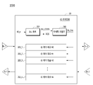
도 4는 일 실시예에 의한 입출력 회로의 구성도이다.
도 5는 일 실시예에 의한 프리-엠퍼시스 회로의 구성도이다.
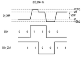
도 6A 및 도 6B는 프리-엠퍼시스 여부에 따른 송신 신호의 파형도이다.
도 7은 일 실시예에 의한 스토리지 시스템의 구성도이다.
도 8 및 도 9는 실시예들에 따른 데이터 처리 시스템의 구성도이다.
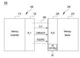
도 10은 일 실시예에 의한 데이터 저장 장치를 포함하는 네트워크 시스템의 구성도이다.
도 11은 일 실시 예에 따른 데이터 저장 장치에 포함된 비휘발성 메모리 장치의 구성도이다.
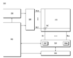
100 : 호스트 장치
110 : 메모리 컨트롤러
120 : 제 1 인터페이스 회로
200 : 저장
210 : 메모리 장치
220 : 제 2 인터페이스 회로
Claims (16)
- 메모리 컨트롤러를 포함하는 호스트 장치; 및
상기 호스트 장치와 인터페이스 회로를 통해 통신하는 메모리 장치를 포함하고,
상기 인터페이스 회로는 지연고정루프 회로에서 생성한 지연코드에 기초하여 상기 호스트 장치로 전송할 송신 신호에 결합할 부가 신호를 생성하도록 구성되는 데이터 저장 장치. - 제 1 항에 있어서,
상기 인터페이스 회로는 상기 지연고정루프 회로; 및
상기 지연코드에 기초하여 결정된 지연시간만큼 상기 송신 신호를 지연시켜 상기 부가 신호를 생성하고, 상기 송신 신호와 상기 부가 신호를 결합하도록 구성되는 프리-엠퍼시스 회로;
를 포함하도록 구성되는 데이터 저장 장치. - 제 2 항에 있어서,
상기 지연시간은 상기 송신 신호의 1UI(Unit Interval)에 대응하는 데이터 저장 장치. - 제 2 항에 있어서,
상기 인터페이스 회로는, 상기 프리-엠퍼시스 회로를 각각 구비하는 복수의 입출력 회로를 포함하고,
상기 지연고정루프 회로는 상기 복수의 입출력 회로와 함께 집적되는 데이터 저장 장치. - 제 1 항에 있어서,
상기 지연고정루프 회로는 파워-업 후 듀티 사이클 보정에 사용되는 클럭 신호에 기초하여 상기 지연코드를 생성하도록 구성되는 데이터 저장 장치. - 제 1 항에 있어서,
상기 인터페이스 회로는, 복수의 입출력 회로를 포함하고,
상기 지연코드는 상기 복수의 입출력 회로 각각으로 제공되는 데이터 저장 장치. - 입출력 제어 회로를 포함하는 인터페이스 회로; 및
상기 인터페이스 회로를 통해 호스트 장치와 데이터를 송수신하는 메모리 장치;를 포함하고,
상기 입출력 제어 회로는, 상기 호스트 장치로부터 전송되는 클럭 신호에 기초하여 내부 클럭신호 및 지연 코드를 생성하는 지연고정루프 회로; 및
상기 지연코드를 수신하여 상기 호스트 장치로 전송할 송신 신호에 결합할 부가 신호를 생성하도록 구성되는 복수의 입출력 회로;
를 포함하도록 구성되는 데이터 저장 장치. - 제 7 항에 있어서,
상기 복수의 입출력 회로 각각은, 상기 지연코드에 기초하여 결정된 지연시간만큼 상기 송신 신호를 지연시켜 상기 부가 신호를 생성하도록 구성되는 프리-엠퍼시스 회로를 포함하도록 구성되는 데이터 저장 장치. - 제 8 항에 있어서,
상기 지연시간은 상기 송신 신호의 1UI(Unit Interval)에 대응하는 데이터 저장 장치. - 제 7 항에 있어서,
상기 지연고정루프 회로는 상기 복수의 입출력 회로와 함께 집적되는 데이터 저장 장치. - 제 7 항에 있어서,
상기 지연고정루프 회로는 파워-업 후 듀티 사이클 보정에 사용되는 클럭 신호에 기초하여 상기 지연코드를 생성하도록 구성되는 데이터 저장 장치. - 메모리 장치를 포함하는 저장부에 구비되는 인터페이스 회로로서,
호스트 장치로부터 전송되는 클럭 신호에 기초하여 내부 클럭신호 및 지연코드를 생성하는 지연고정루프 회로; 및
상기 지연코드를 수신하여 상기 호스트 장치로 전송할 송신 신호에 결합할 부가 신호를 생성하도록 구성되는 복수의 입출력 회로;
를 포함하도록 구성되는 인터페이스 회로. - 제 12 항에 있어서,
상기 복수의 입출력 회로 각각은, 상기 지연코드에 기초하여 결정된 지연시간만큼 상기 송신 신호를 지연시켜 상기 부가 신호를 생성하도록 구성되는 프리-엠퍼시스 회로를 포함하도록 구성되는 인터페이스 회로. - 제 13 항에 있어서,
상기 지연시간은 상기 송신 신호의 1UI(Unit Interval)에 대응하는 인터페이스 회로. - 제 12 항에 있어서,
상기 지연고정루프회로는 상기 복수의 입출력 회로와 함께 집적되는 인터페이스 회로. - 제 12 항에 있어서,
상기 인터페이스 회로는 파워-업 동작 후 듀티 사이클 보정에 사용되는 클럭 신호에 기초하여 상기 지연코드를 생성하도록 구성되는 인터페이스 회로.
Priority Applications (3)
| Application Number | Priority Date | Filing Date | Title |
|---|---|---|---|
| KR1020210032790A KR102915284B1 (ko) | 2021-03-12 | 2021-03-12 | 데이터 저장 장치 및 이를 위한 인터페이스 회로 |
| US17/393,001 US11704051B2 (en) | 2021-03-12 | 2021-08-03 | Data storage apparatus and interface circuit therefor |
| CN202111323388.5A CN115083458A (zh) | 2021-03-12 | 2021-11-08 | 数据存储设备及其接口电路 |
Applications Claiming Priority (1)
| Application Number | Priority Date | Filing Date | Title |
|---|---|---|---|
| KR1020210032790A KR102915284B1 (ko) | 2021-03-12 | 2021-03-12 | 데이터 저장 장치 및 이를 위한 인터페이스 회로 |
Publications (2)
| Publication Number | Publication Date |
|---|---|
| KR20220128126A true KR20220128126A (ko) | 2022-09-20 |
| KR102915284B1 KR102915284B1 (ko) | 2026-01-22 |
Family
ID=83193803
Family Applications (1)
| Application Number | Title | Priority Date | Filing Date |
|---|---|---|---|
| KR1020210032790A Active KR102915284B1 (ko) | 2021-03-12 | 2021-03-12 | 데이터 저장 장치 및 이를 위한 인터페이스 회로 |
Country Status (3)
| Country | Link |
|---|---|
| US (1) | US11704051B2 (ko) |
| KR (1) | KR102915284B1 (ko) |
| CN (1) | CN115083458A (ko) |
Cited By (1)
| Publication number | Priority date | Publication date | Assignee | Title |
|---|---|---|---|---|
| KR102730366B1 (ko) * | 2023-06-27 | 2024-11-14 | 주식회사 엑시콘 | 신호 동기화를 위한 테스트 장치 및 방법 |
Families Citing this family (3)
| Publication number | Priority date | Publication date | Assignee | Title |
|---|---|---|---|---|
| US12206530B2 (en) * | 2022-01-06 | 2025-01-21 | Brookhaven Science Associates, Llc | User-configurable high-speed line driver |
| US12175118B2 (en) * | 2022-03-22 | 2024-12-24 | Silicon Laboratories Inc. | External nonvolatile memory with additional functionality |
| JP7655975B2 (ja) * | 2023-07-13 | 2025-04-02 | レノボ・シンガポール・プライベート・リミテッド | 情報処理装置、及び制御方法 |
Family Cites Families (10)
| Publication number | Priority date | Publication date | Assignee | Title |
|---|---|---|---|---|
| US7440340B2 (en) * | 2004-10-19 | 2008-10-21 | Samsung Electronics Co., Ltd. | Output buffer of a semiconductor memory device |
| KR100695002B1 (ko) * | 2005-09-15 | 2007-03-13 | 주식회사 하이닉스반도체 | 자동 리셋 기능을 가지는 dll |
| KR100862233B1 (ko) | 2007-01-04 | 2008-10-09 | 한국과학기술원 | 지연 시간을 가변할 수 있는 탭 지연선을 구비하는 프리엠퍼시스 출력 회로 |
| KR101045071B1 (ko) | 2009-11-30 | 2011-06-29 | 주식회사 하이닉스반도체 | 데이터 출력회로 |
| US8760188B2 (en) * | 2011-06-30 | 2014-06-24 | Silicon Image, Inc. | Configurable multi-dimensional driver and receiver |
| KR20150134002A (ko) | 2014-05-21 | 2015-12-01 | 에스케이하이닉스 주식회사 | 반도체 장치 |
| US9971733B1 (en) | 2014-12-04 | 2018-05-15 | Altera Corporation | Scalable 2.5D interface circuitry |
| US10528515B2 (en) * | 2017-06-27 | 2020-01-07 | Intel Corporation | Memory channel driver with echo cancellation |
| US10530617B2 (en) | 2017-08-07 | 2020-01-07 | Micron Technology, Inc. | Programmable channel equalization for multi-level signaling |
| KR20190051314A (ko) | 2017-11-06 | 2019-05-15 | 삼성전자주식회사 | 포스트 엠퍼시스 신호를 출력하기 위한 전자 회로 |
-
2021
- 2021-03-12 KR KR1020210032790A patent/KR102915284B1/ko active Active
- 2021-08-03 US US17/393,001 patent/US11704051B2/en active Active
- 2021-11-08 CN CN202111323388.5A patent/CN115083458A/zh active Pending
Cited By (1)
| Publication number | Priority date | Publication date | Assignee | Title |
|---|---|---|---|---|
| KR102730366B1 (ko) * | 2023-06-27 | 2024-11-14 | 주식회사 엑시콘 | 신호 동기화를 위한 테스트 장치 및 방법 |
Also Published As
| Publication number | Publication date |
|---|---|
| US20220291863A1 (en) | 2022-09-15 |
| US11704051B2 (en) | 2023-07-18 |
| CN115083458A (zh) | 2022-09-20 |
| KR102915284B1 (ko) | 2026-01-22 |
Similar Documents
| Publication | Publication Date | Title |
|---|---|---|
| US11500770B2 (en) | Memory device controlling including reading from a first memory and writing to a second memory based on timing and control signals | |
| KR102915284B1 (ko) | 데이터 저장 장치 및 이를 위한 인터페이스 회로 | |
| US9971521B2 (en) | Memory devices, systems and methods employing command/address calibration | |
| US10133284B2 (en) | Circuits for setting reference voltages and semiconductor devices including the same | |
| US10068633B2 (en) | Semiconductor devices and integrated circuits including the same | |
| KR20190120526A (ko) | 메모리 장치 및 이의 동작 방법 | |
| US20250370869A1 (en) | Soft read operations with progressive data output | |
| KR102805363B1 (ko) | 메모리 컨트롤러, 및 이를 포함하는 스토리지 장치, 및 메모리 시스템 | |
| US11036433B2 (en) | Memory controller, data storage device, and storage system having the same | |
| US20220294445A1 (en) | Computer system and interface circuit therefor | |
| CN113889161A (zh) | 配置存储器子系统的多个寄存器时钟驱动器 | |
| US11211112B2 (en) | Semiconductor devices controlling column operation of banks | |
| US12237037B2 (en) | Device of generating reference voltages for multi-level signaling and memory system including the same | |
| KR20220111487A (ko) | 메모리 시스템 |
Legal Events
| Date | Code | Title | Description |
|---|---|---|---|
| PA0109 | Patent application |
St.27 status event code: A-0-1-A10-A12-nap-PA0109 |
|
| PG1501 | Laying open of application |
St.27 status event code: A-1-1-Q10-Q12-nap-PG1501 |
|
| PA0201 | Request for examination |
St.27 status event code: A-1-2-D10-D11-exm-PA0201 |
|
| E902 | Notification of reason for refusal | ||
| PE0902 | Notice of grounds for rejection |
St.27 status event code: A-1-2-D10-D21-exm-PE0902 |
|
| P11-X000 | Amendment of application requested |
St.27 status event code: A-2-2-P10-P11-nap-X000 |
|
| E601 | Decision to refuse application | ||
| PE0601 | Decision on rejection of patent |
St.27 status event code: N-2-6-B10-B15-exm-PE0601 |
|
| E13 | Pre-grant limitation requested |
Free format text: ST27 STATUS EVENT CODE: A-2-3-E10-E13-LIM-X000 (AS PROVIDED BY THE NATIONAL OFFICE) |
|
| E13-X000 | Pre-grant limitation requested |
St.27 status event code: A-2-3-E10-E13-lim-X000 |
|
| P11 | Amendment of application requested |
Free format text: ST27 STATUS EVENT CODE: A-2-2-P10-P11-NAP-X000 (AS PROVIDED BY THE NATIONAL OFFICE) |
|
| P11-X000 | Amendment of application requested |
St.27 status event code: A-2-2-P10-P11-nap-X000 |
|
| F13 | Ip right granted in full following pre-grant review |
Free format text: ST27 STATUS EVENT CODE: A-3-4-F10-F13-REX-PX0701 (AS PROVIDED BY THE NATIONAL OFFICE) |
|
| PX0701 | Decision of registration after re-examination |
St.27 status event code: A-3-4-F10-F13-rex-PX0701 |
|
| PG1601 | Publication of registration |
St.27 status event code: A-4-4-Q10-Q13-nap-PG1601 |
|
| Q13 | Ip right document published |
Free format text: ST27 STATUS EVENT CODE: A-4-4-Q10-Q13-NAP-PG1601 (AS PROVIDED BY THE NATIONAL OFFICE) |