KR20220128126A - Data storage device and interface circuit therefor - Google Patents
Data storage device and interface circuit therefor Download PDFInfo
- Publication number
- KR20220128126A KR20220128126A KR1020210032790A KR20210032790A KR20220128126A KR 20220128126 A KR20220128126 A KR 20220128126A KR 1020210032790 A KR1020210032790 A KR 1020210032790A KR 20210032790 A KR20210032790 A KR 20210032790A KR 20220128126 A KR20220128126 A KR 20220128126A
- Authority
- KR
- South Korea
- Prior art keywords
- delay
- signal
- circuit
- interface circuit
- host device
- Prior art date
- Legal status (The legal status is an assumption and is not a legal conclusion. Google has not performed a legal analysis and makes no representation as to the accuracy of the status listed.)
- Granted
Links
Images


Classifications
-
- G—PHYSICS
- G11—INFORMATION STORAGE
- G11C—STATIC STORES
- G11C7/00—Arrangements for writing information into, or reading information out from, a digital store
- G11C7/10—Input/output [I/O] data interface arrangements, e.g. I/O data control circuits, I/O data buffers
- G11C7/1078—Data input circuits, e.g. write amplifiers, data input buffers, data input registers, data input level conversion circuits
- G11C7/1093—Input synchronization
-
- G—PHYSICS
- G11—INFORMATION STORAGE
- G11C—STATIC STORES
- G11C7/00—Arrangements for writing information into, or reading information out from, a digital store
- G11C7/10—Input/output [I/O] data interface arrangements, e.g. I/O data control circuits, I/O data buffers
- G11C7/1051—Data output circuits, e.g. read-out amplifiers, data output buffers, data output registers, data output level conversion circuits
-
- G—PHYSICS
- G06—COMPUTING OR CALCULATING; COUNTING
- G06F—ELECTRIC DIGITAL DATA PROCESSING
- G06F3/00—Input arrangements for transferring data to be processed into a form capable of being handled by the computer; Output arrangements for transferring data from processing unit to output unit, e.g. interface arrangements
- G06F3/06—Digital input from, or digital output to, record carriers, e.g. RAID, emulated record carriers or networked record carriers
- G06F3/0601—Interfaces specially adapted for storage systems
- G06F3/0628—Interfaces specially adapted for storage systems making use of a particular technique
- G06F3/0655—Vertical data movement, i.e. input-output transfer; data movement between one or more hosts and one or more storage devices
-
- G—PHYSICS
- G06—COMPUTING OR CALCULATING; COUNTING
- G06F—ELECTRIC DIGITAL DATA PROCESSING
- G06F1/00—Details not covered by groups G06F3/00 - G06F13/00 and G06F21/00
- G06F1/04—Generating or distributing clock signals or signals derived directly therefrom
-
- G—PHYSICS
- G06—COMPUTING OR CALCULATING; COUNTING
- G06F—ELECTRIC DIGITAL DATA PROCESSING
- G06F1/00—Details not covered by groups G06F3/00 - G06F13/00 and G06F21/00
- G06F1/04—Generating or distributing clock signals or signals derived directly therefrom
- G06F1/06—Clock generators producing several clock signals
-
- G—PHYSICS
- G06—COMPUTING OR CALCULATING; COUNTING
- G06F—ELECTRIC DIGITAL DATA PROCESSING
- G06F3/00—Input arrangements for transferring data to be processed into a form capable of being handled by the computer; Output arrangements for transferring data from processing unit to output unit, e.g. interface arrangements
- G06F3/06—Digital input from, or digital output to, record carriers, e.g. RAID, emulated record carriers or networked record carriers
- G06F3/0601—Interfaces specially adapted for storage systems
- G06F3/0602—Interfaces specially adapted for storage systems specifically adapted to achieve a particular effect
- G06F3/061—Improving I/O performance
-
- G—PHYSICS
- G06—COMPUTING OR CALCULATING; COUNTING
- G06F—ELECTRIC DIGITAL DATA PROCESSING
- G06F3/00—Input arrangements for transferring data to be processed into a form capable of being handled by the computer; Output arrangements for transferring data from processing unit to output unit, e.g. interface arrangements
- G06F3/06—Digital input from, or digital output to, record carriers, e.g. RAID, emulated record carriers or networked record carriers
- G06F3/0601—Interfaces specially adapted for storage systems
- G06F3/0628—Interfaces specially adapted for storage systems making use of a particular technique
- G06F3/0655—Vertical data movement, i.e. input-output transfer; data movement between one or more hosts and one or more storage devices
- G06F3/0658—Controller construction arrangements
-
- G—PHYSICS
- G06—COMPUTING OR CALCULATING; COUNTING
- G06F—ELECTRIC DIGITAL DATA PROCESSING
- G06F3/00—Input arrangements for transferring data to be processed into a form capable of being handled by the computer; Output arrangements for transferring data from processing unit to output unit, e.g. interface arrangements
- G06F3/06—Digital input from, or digital output to, record carriers, e.g. RAID, emulated record carriers or networked record carriers
- G06F3/0601—Interfaces specially adapted for storage systems
- G06F3/0668—Interfaces specially adapted for storage systems adopting a particular infrastructure
- G06F3/0671—In-line storage system
- G06F3/0673—Single storage device
- G06F3/0679—Non-volatile semiconductor memory device, e.g. flash memory, one time programmable memory [OTP]
-
- G—PHYSICS
- G11—INFORMATION STORAGE
- G11C—STATIC STORES
- G11C7/00—Arrangements for writing information into, or reading information out from, a digital store
- G11C7/10—Input/output [I/O] data interface arrangements, e.g. I/O data control circuits, I/O data buffers
- G11C7/1051—Data output circuits, e.g. read-out amplifiers, data output buffers, data output registers, data output level conversion circuits
- G11C7/1066—Output synchronization
-
- G—PHYSICS
- G11—INFORMATION STORAGE
- G11C—STATIC STORES
- G11C7/00—Arrangements for writing information into, or reading information out from, a digital store
- G11C7/10—Input/output [I/O] data interface arrangements, e.g. I/O data control circuits, I/O data buffers
- G11C7/1078—Data input circuits, e.g. write amplifiers, data input buffers, data input registers, data input level conversion circuits
-
- G—PHYSICS
- G11—INFORMATION STORAGE
- G11C—STATIC STORES
- G11C7/00—Arrangements for writing information into, or reading information out from, a digital store
- G11C7/12—Bit line control circuits, e.g. drivers, boosters, pull-up circuits, pull-down circuits, precharging circuits, equalising circuits, for bit lines
-
- G—PHYSICS
- G11—INFORMATION STORAGE
- G11C—STATIC STORES
- G11C7/00—Arrangements for writing information into, or reading information out from, a digital store
- G11C7/22—Read-write [R-W] timing or clocking circuits; Read-write [R-W] control signal generators or management
- G11C7/222—Clock generating, synchronizing or distributing circuits within memory device
-
- G—PHYSICS
- G11—INFORMATION STORAGE
- G11C—STATIC STORES
- G11C8/00—Arrangements for selecting an address in a digital store
- G11C8/08—Word line control circuits, e.g. drivers, boosters, pull-up circuits, pull-down circuits, precharging circuits, for word lines
-
- H—ELECTRICITY
- H03—ELECTRONIC CIRCUITRY
- H03K—PULSE TECHNIQUE
- H03K5/00—Manipulating of pulses not covered by one of the other main groups of this subclass
- H03K5/156—Arrangements in which a continuous pulse train is transformed into a train having a desired pattern
- H03K5/1565—Arrangements in which a continuous pulse train is transformed into a train having a desired pattern the output pulses having a constant duty cycle
-
- H—ELECTRICITY
- H03—ELECTRONIC CIRCUITRY
- H03L—AUTOMATIC CONTROL, STARTING, SYNCHRONISATION OR STABILISATION OF GENERATORS OF ELECTRONIC OSCILLATIONS OR PULSES
- H03L7/00—Automatic control of frequency or phase; Synchronisation
- H03L7/06—Automatic control of frequency or phase; Synchronisation using a reference signal applied to a frequency- or phase-locked loop
- H03L7/08—Details of the phase-locked loop
- H03L7/081—Details of the phase-locked loop provided with an additional controlled phase shifter
- H03L7/0812—Details of the phase-locked loop provided with an additional controlled phase shifter and where no voltage or current controlled oscillator is used
- H03L7/0814—Details of the phase-locked loop provided with an additional controlled phase shifter and where no voltage or current controlled oscillator is used the phase shifting device being digitally controlled
-
- G—PHYSICS
- G11—INFORMATION STORAGE
- G11C—STATIC STORES
- G11C7/00—Arrangements for writing information into, or reading information out from, a digital store
- G11C7/10—Input/output [I/O] data interface arrangements, e.g. I/O data control circuits, I/O data buffers
- G11C7/1078—Data input circuits, e.g. write amplifiers, data input buffers, data input registers, data input level conversion circuits
- G11C7/1084—Data input buffers, e.g. comprising level conversion circuits, circuits for adapting load
Landscapes
- Engineering & Computer Science (AREA)
- Theoretical Computer Science (AREA)
- Physics & Mathematics (AREA)
- General Engineering & Computer Science (AREA)
- General Physics & Mathematics (AREA)
- Human Computer Interaction (AREA)
- Nonlinear Science (AREA)
- Microelectronics & Electronic Packaging (AREA)
- Memory System (AREA)
- Logic Circuits (AREA)
- Input Circuits Of Receivers And Coupling Of Receivers And Audio Equipment (AREA)
- Communication Control (AREA)
- Dram (AREA)
Abstract
일 실시예에 의한 데이터 처리 장치는 메모리 컨트롤러를 포함하는 호스트 장치 및, 호스트 장치와 인터페이스 회로를 통해 통신하는 메모리 장치를 포함하고, 인터페이스 회로는 지연고정루프 회로에서 생성한 지연코드에 기초하여 호스트 장치로 전송할 송신 신호에 결합할 부가 신호를 생성하도록 구성될 수 있다.A data processing apparatus according to an embodiment includes a host device including a memory controller, and a memory device communicating with the host device through an interface circuit, wherein the interface circuit is based on a delay code generated by a delay locked loop circuit. may be configured to generate an additional signal to be combined with a transmit signal to be transmitted to the .
Description
본 기술은 반도체 집적 장치에 관한 것으로, 보다 구체적으로는 데이터 저장 장치 및 이를 위한 인터페이스 회로에 관한 것이다.The present technology relates to a semiconductor integrated device, and more particularly, to a data storage device and an interface circuit therefor.
데이터 저장 장치는 데이터가 저장되는 메모리 장치 및 호스트 장치의 요청에 응답하여 메모리 장치와 데이터를 송수신하는 컨트롤러를 포함할 수 있다. 메모리 장치와 컨트롤러는 인터페이스 회로 및 채널을 통해 데이터를 송수신한다.The data storage device may include a memory device in which data is stored and a controller that transmits/receives data to and from the memory device in response to a request from the host device. The memory device and the controller transmit and receive data through interface circuits and channels.
메모리 장치와 컨트롤러 간에 송수신되는 데이터의 무결성을 보장하기 위해 프리-엠퍼시스(Pre-Emphasis) 기법이 제안되었다.In order to ensure the integrity of data transmitted and received between the memory device and the controller, a pre-emphasis technique has been proposed.
프리-엠퍼시스 기법은 송신할 데이터의 논리 레벨이 천이되는 구간에 부가 신호를 추가하여 채널을 통과하는 신호의 왜곡을 방지하는 기법이다.The pre-emphasis technique is a technique for preventing distortion of a signal passing through a channel by adding an additional signal to a section in which the logic level of data to be transmitted is transitioned.
프리-엠퍼시스를 위한 부가 신호는 송신할 데이터를 일정 시간 지연시켜 생성할 수 있으며, 이를 위해 지연 시간을 정확하게 제어할 필요가 있다.The additional signal for pre-emphasis may be generated by delaying data to be transmitted by a predetermined time, and for this purpose, it is necessary to accurately control the delay time.
데이터 저장 장치의 고용량화 및 고속화에 따라 인터페이스 회로에 구비되는 단위 입출력 회로의 수가 증가하며, 각 입출력 회로에 제공할 부가 신호를 정확하고 효율적으로 생성할 것이 요구된다.The number of unit input/output circuits provided in the interface circuit increases with the increase in capacity and speed of the data storage device, and it is required to accurately and efficiently generate additional signals to be provided to each input/output circuit.
본 기술의 실시예는 인터페이스 회로 내에 구비된 지연 고정 루프(Delayed Locked Loop; DLL) 회로에서 생성한 지연 코드에 기초하여 프리-엠퍼시스에 사용할 부가 신호를 생성하여 프리-엠퍼시스 동작을 수행할 수 있는 데이터 저장 장치 및 이를 위한 인터페이스 회로를 제공할 수 있다.An embodiment of the present technology may perform a pre-emphasis operation by generating an additional signal to be used for pre-emphasis based on a delay code generated by a Delayed Locked Loop (DLL) circuit provided in the interface circuit. A data storage device and an interface circuit therefor may be provided.
본 기술의 일 실시예에 의한 데이터 저장 장치는 메모리 컨트롤러를 포함하는 호스트 장치; 및 상기 호스트 장치와 인터페이스 회로를 통해 통신하는 메모리 장치를 포함하고, 상기 인터페이스 회로는 지연고정루프 회로에서 생성한 지연코드에 기초하여 상기 호스트 장치로 전송할 송신 신호에 결합할 부가 신호를 생성하도록 구성될 수 있다.A data storage device according to an embodiment of the present technology includes a host device including a memory controller; and a memory device in communication with the host device via an interface circuit, wherein the interface circuit is configured to generate an additional signal to be coupled to a transmission signal to be transmitted to the host device based on the delay code generated by the delay locked loop circuit. can
본 기술의 일 실시예에 의한 데이터 저장 장치는 입출력 제어 회로를 포함하는 인터페이스 회로; 및 상기 인터페이스 회로를 통해 호스트 장치와 데이터를 송수신하는 메모리 장치;를 포함하고, 상기 입출력 제어 회로는, 상기 호스트 장치로부터 전송되는 클럭 신호에 기초하여 내부 클럭신호 및 지연 코드를 생성하는 지연고정루프 회로; 및 상기 지연코드를 수신하여 상기 호스트 장치로 전송할 송신 신호에 결합할 부가 신호를 생성하도록 구성되는 복수의 입출력 회로;를 포함하도록 구성될 수 있다.A data storage device according to an embodiment of the present technology includes an interface circuit including an input/output control circuit; and a memory device for transmitting and receiving data to and from a host device through the interface circuit, wherein the input/output control circuit includes a delay locked loop circuit that generates an internal clock signal and a delay code based on a clock signal transmitted from the host device. ; and a plurality of input/output circuits configured to receive the delay code and generate an additional signal to be coupled to a transmission signal to be transmitted to the host device.
본 기술의 일 실시예에 의한 인터페이스 회로는 메모리 장치를 포함하는 저장부에 구비되는 인터페이스 회로로서, 호스트 장치로부터 전송되는 클럭 신호에 기초하여 내부 클럭신호 및 지연코드를 생성하는 지연고정루프 회로; 및 상기 지연코드를 수신하여 상기 호스트 장치로 전송할 송신 신호에 결합할 부가 신호를 생성하도록 구성되는 복수의 입출력 회로;를 포함하도록 구성될 수 있다.An interface circuit according to an embodiment of the present technology is an interface circuit provided in a storage unit including a memory device, and includes: a delay locked loop circuit for generating an internal clock signal and a delay code based on a clock signal transmitted from a host device; and a plurality of input/output circuits configured to receive the delay code and generate an additional signal to be coupled to a transmission signal to be transmitted to the host device.
본 기술에 의하면, 인터페이스 회로 내의 지연 고정 루프 회로에서 생성한 지연 코드를 이용하여 송신 신호를 목표 시간만큼 정확히 지연시켜 프리-엠퍼시스용 부가 신호를 생성할 수 있다.According to the present technology, an additional signal for pre-emphasis can be generated by accurately delaying a transmission signal by a target time using the delay code generated by the delay locked loop circuit in the interface circuit.
프리-엠퍼시스에 필요한 부가 신호를 생성하기 위한 회로가 인터페이스 회로 내에 통합됨에 따라 별도의 지연 회로를 추가할 필요가 없어 면적 효율이 증대되고 고속 동작의 신뢰성을 향상시킬 수 있다.As a circuit for generating an additional signal required for pre-emphasis is integrated in the interface circuit, there is no need to add a separate delay circuit, so that area efficiency is increased and reliability of high-speed operation can be improved.
도 1은 일 실시예에 의한 데이터 저장 장치의 구성도이다.
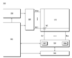
도 2는 일 실시예에 의한 인터페이스 회로의 구성도이다.
도 3은 일 실시예에 의한 지연 고정 루프 회로의 구성도이다.
도 4는 일 실시예에 의한 입출력 회로의 구성도이다.
도 5는 일 실시예에 의한 프리-엠퍼시스 회로의 구성도이다.
도 6A 및 도 6B는 프리-엠퍼시스 여부에 따른 송신 신호의 파형도이다.
도 7은 일 실시예에 의한 스토리지 시스템의 구성도이다.
도 8 및 도 9는 실시예들에 따른 데이터 처리 시스템의 구성도이다.
도 10은 일 실시예에 의한 데이터 저장 장치를 포함하는 네트워크 시스템의 구성도이다.
도 11은 일 실시 예에 따른 데이터 저장 장치에 포함된 비휘발성 메모리 장치의 구성도이다.1 is a block diagram of a data storage device according to an exemplary embodiment.
2 is a block diagram of an interface circuit according to an embodiment.
3 is a block diagram of a delay locked loop circuit according to an embodiment.
4 is a block diagram of an input/output circuit according to an embodiment.
5 is a block diagram of a pre-emphasis circuit according to an embodiment.
6A and 6B are waveform diagrams of a transmission signal according to whether pre-emphasis is applied.
7 is a configuration diagram of a storage system according to an exemplary embodiment.
8 and 9 are block diagrams of data processing systems according to embodiments.
10 is a block diagram of a network system including a data storage device according to an embodiment.
11 is a block diagram of a nonvolatile memory device included in a data storage device according to an exemplary embodiment.
이하, 첨부된 도면을 참조하여 본 기술의 실시예를 보다 구체적으로 설명한다.Hereinafter, embodiments of the present technology will be described in more detail with reference to the accompanying drawings.
도 1은 일 실시예에 의한 데이터 저장 장치의 구성도이다.1 is a block diagram of a data storage device according to an exemplary embodiment.
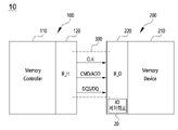
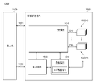
데이터 저장 장치(10)는 호스트 장치(100) 및 호스트 장치(100)와 채널(300)을 통해 접속되는 저장부(200)를 포함할 수 있다.The
호스트 장치(100)는 저장부(200)를 제어하기 위한 메모리 컨트롤러(110) 및 호스트 측 인터페이스 회로(IF_H)인 제 1 인터페이스 회로(120)를 포함할 수 있다. 저장부(200)는 메모리 장치(210) 및 메모리측 인터페이스 회로(IF_D)인 제 2 인터페이스 회로(220)를 포함할 수 있다.The
호스트 장치(100)는 프로세서 및 프로세서의 제어에 따라 동작하는 복수의 IP를 포함할 수 있다. 호스트 장치(100)는 여러가지 기능을 가진 복수의 기능 블록, 예를 들어 IP들을 하나의 칩으로 구현한 SoC(System on Chip)일 수 있다. 제 1 인터페이스 회로(120) 또한 하나의 IP로서 SoC로 구현된 호스트 장치(100) 내에 집적될 수 있다.The
메모리 장치(210)는 DRAM(Dynamic Random Access Memory), SRAM(Static Random Access Memory), TRAM(Thyristor Random Access Memory) 등과 같은 휘발성 메모리 소자 중에서 선택된 메모리 소자를 이용하여 구현될 수 있다.The
메모리 장치(210)는 EEPROM(Electrically Erasable and Programmable ROM), 낸드(NAND) 플래시 메모리, 노어(NOR) 플래시 메모리, PRAM(Phase-Change RAM), ReRAM(Resistive RAM) FRAM(Ferroelectric RAM), STT-MRAM(Spin Torque Transfer Magnetic RAM) 등과 같은 다양한 비휘발성 메모리 소자 중에서 선택된 메모리 소자를 이용하여 구현될 수 있고, 솔리드 스테이트 드라이브(SSD), 메모리 카드, 유니버설 플래시 기억장치(UFS) 등의 형태로 구현될 수 있다. 메모리 장치(210)는 복수의 다이들, 또는 복수의 칩들, 또는 복수의 패키지들을 포함할 수 있다. 나아가 메모리 장치(210)는 하나의 메모리 셀에 한 비트의 데이터를 저장하는 싱글 레벨 셀(Single-Level Cell), 또는 하나의 메모리 셀에 복수 비트의 데이터를 저장하는 멀티 레벨 셀(Multi-Level Cell)로 동작할 수 있다.The
채널(300)은 호스트 장치(100)와 데이터 저장 장치(200) 간에 송수신되는 신호를 전달하는 경로이다.The
호스트 장치(100)는 제 1 인터페이스 회로(120)를 통해 제 2 인터페이스 회로(220)로 클럭(CLK) 신호, 커맨드(CMD) 신호, 어드레스(ADD) 신호 등을 전송할 수 있다. 또한, 호스트 장치(100)는 제 1 인터페이스 회로(120)를 통해 저장부(200)로 데이터 스트로브 신호(DQS)에 동기하여 데이터(DQ)를 전송할 수 있다.The
저장부(200)는 제 2 인터페이스 회로(220)를 통해 호스트 장치(100)로로 데이터 스트로브 신호(DQS)에 동기하여 데이터(DQ)를 전송할 수 있다.The
호스트 장치(100)에서 저장부(200)로 데이터 스트로브 신호(DQS) 및 데이터(DQ)를 전송하는 경로는 저장부(200)가 호스트 장치(100)로 데이터 스트로브 신호(DQS 및 데이터(DQ)를 전송하는 경로와 동일하고 공유될 수 있다. 따라서 호스트 장치(100)에서 저장부(200)로 출력되는 데이터 스트로브 신호(DQS) 및 데이터(DQ)는 쓰기 DQS 및 쓰기 DQ로 지칭될 수 있고, 저장부(200)에서 호스트 장치(100)로 출력되는 데이터 스트로브 신호(DQS) 및 데이터(DQ)는 읽기 DQS 및 읽기 DQ로 지칭될 수 있다.A path through which the data strobe signal DQS and data DQ are transmitted from the
DDR(Double Data Rate) 이상의 고속 동작 속도를 갖는 메모리 장치(210)는 내부 클럭의 라이징 에지(rising edge)와 폴링 에지(falling edge)를 모두 이용하기 때문에 내부 클럭의 듀티 사이클(duty cycle)을 50%로 유지하는 것이 중요하다.Since the
이를 위해 제 2 인터페이스 회로(220)는 파워-업 동작시 호스트 장치(100)로부터 수신한 외부 클럭 신호(CLK)로부터 생성된 내부 클럭의 듀티 사이클을 50%로 맞추기 위한 DCC(Duty Cycle Correction) 트레이닝 동작을 수행할 수 있다. 일 실시예에서, 제 2 인터페이스 회로(220)는 DCC 트레이닝 동작시 외부 클럭 신호(CLK)에 동기하여 메모리 장치(210)로 리드 인에이블 신호(RE_t/c)를 전송하여 DDR로 페이지 리드를 수행할 수 있다.To this end, the
저장부(200)는 또한 DCC 트레이닝에 의해 듀티 사이클이 보정된 클럭 신호의 스큐를 보정하여 지연 고정된 내부클럭을 생성하기 위한 DLL 회로를 포함할 수 있다. DLL 회로는 내부 클럭신호가 반도체 메모리 장치 내부의 데이터 출력단까지 전달되는 과정에서 발생하는 지연성분을 보상할 수 있도록 내부 클럭신호의 지연량을 보정하는 회로일 수 있다.The
일 실시예에서, 제 2 인터페이스 회로(220)는 복수의 입출력(IO) 제어 회로(20)를 포함할 수 있다. DLL 회로는 DCC 트레이닝에 사용되는 리드 인에이블 신호(RE_t)에 응답하여 생성된 지연코드에 따라 지연고정된 내부 클럭신호를 생성하는 디지털 회로로 구현되어 IO 제어 회로(20) 내에 집적될 수 있다.In an embodiment, the
제 2 인터페이스 회로(220)는 메모리 장치(210)로부터 리드된 데이터가 채널(300)을 경유하여 호스트 장치(100)로 전송되는 과정에서 발생할 수 있는 신호 감쇄 또는 노이즈에 의한 영향을 방지하기 위하여 프리-엠퍼시스 동작을 수행할 수 있다.The
일 실시예에서, 제 2 인터페이스 회로(220)는 DCC 트레이닝 동작과 함께 입출력 제어회로(20) 내의 DLL회로를 동작시켜 생성한 지연코드에 기초하여 송신 신호를 목표 시간(1 Unit Delay) 만큼 지연시켜 프리-엠퍼시스용 부가 신호를 생성하고, 이 부가 신호를 송신 신호와 결합하는 프리-엠퍼시스 동작을 수행할 수 있다.In one embodiment, the
메모리 장치(210)의 고용량화에 따라 IO 제어 회로(20)에는 복수의 IO 회로가 구비될 수 있다. 프리-엠퍼시스를 위해 IO 제어 회로(20)의 외부에서 송신 신호를 지연시켜 IO 제어 회로(20)로 공급하는 경우에는, 별도의 지연 회로가 추가되어야 하므로 지연 회로를 위한 추가 면적이 필요하고, IP의 배치를 변경해야 하는 등의 추가 작업이 수반될 수 있다.As the
본 기술에 의하면, IO 제어 회로(20) 내에서 지연코드를 생성하고, 이를 이용하여 송신 데이터를 프리-엠퍼시스할 수 있다. 따라서, 송신 신호를 지연하기 위한 별도의 회로나 IP를 추가할 필요가 없어 면적 효율이 증대되고 고속 동작의 신뢰성을 보장할 수 있다.According to the present technology, it is possible to generate a delay code in the
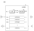
도 2는 일 실시예에 의한 인터페이스 회로의 구성도로서, 예를 들어 제 2 인터페이스 회로(220)를 나타낸다.2 is a block diagram of an interface circuit according to an embodiment, and shows, for example, a
도 2를 참조하면, 일 실시예에 의한 제 2 인터페이스 회로(220)는 송신 드라이버(Tx1, Tx2)와 수신 드라이버(Rx1, Rx2) 사이에서 신호를 송수신하는 IO 제어 회로(20)를 포함할 수 있다.Referring to FIG. 2 , the
IO 제어 회로(20)는 DLL 회로(201), 타이밍 조절부(203) 및 복수의 IO 회로(205, 205-1~205-n)를 포함할 수 있다.The
DLL 회로(201)는 DCC 트레이닝 동작에 사용되는 리드 인에이블 신호(RE_t)를 제공받아 내부 클럭의 지연량을 고정하기 위한 지연코드(DLL_CODE)를 생성하여 지연고정된 내부 클럭신호(DQS)를 출력할 수 있다.The
한편, 리드 동작시 내부 클럭신호(DQS)은 호스트 장치(100)로 전송되어 내부 클럭신호(DQS)와 동기하여 데이터(DQ)를 전송할 때 호스트 장치(100)와 저장부(200)의 동작 타이밍이 동기되도록 할 수 있다.Meanwhile, during a read operation, the internal clock signal DQS is transmitted to the
타이밍 조절부(203)는 지연코드(DLL_CODE)를 수신하여, 지연 제어 신호(DL_CAL)를 생성할 수 있다. 송신 신호의 천이 시점에 송신 신호를 강조하는 프리-엠퍼시스 동작을 수행하기 위해서는 송신 신호를 1UI(Unit Interval) 만큼 지연시켜 부가 신호를 생성하므로, 타이밍 조절부(203)는 클럭의 1주기(2UI)에 대응하는 지연코드(DLL_CODE)를 1/2하여 1UI 해당하는 지연 제어 신호(DL_CAL)를 생성할 수 있다.The
복수의 IO 회로(205-1~205-n)는 각각 지연 제어 신호(DL_CAL)를 수신하여 송신 신호를 지연시켜 부가 신호를 생성하고, 송신 신호에 부가 신호를 결합하여 호스트 장치(100)로 전송하도록 구성된다. IO 회로(205-1~205-n)의 구체적인 설명은 도 4 및 도 5를 참조하여 후술할 것이다.The plurality of IO circuits 205-1 to 205-n receive the delay control signal DL_CAL, respectively, to delay the transmission signal to generate an additional signal, and to combine the additional signal with the transmission signal and transmit it to the
도 3은 일 실시예에 의한 지연 루프 회로의 구성도이다.3 is a block diagram of a delay loop circuit according to an embodiment.
도 3을 참조하면, 일 실시예에 의한 DLL 회로(201)는 내부 클럭 생성부(2011), 지연코드 생성부(2013), 지연고정 클럭 생성부(2015) 및 비교부(2017)를 포함할 수 있다.Referring to FIG. 3 , the
내부 클럭 생성부(2011)는 DCC 트레이닝에 사용되는 클럭 신호, 예를 들어 리드 인에이블 신호(RE_t)로부터 예비 클럭신호(iRE_t)를 생성할 수 있다.The
지연코드 생성부(2013)는 인에이블 신호(CAL_EN)에 응답하여, 비교신호(COMP)에 응답하여 예비 클럭 신호(iRE_t)를 지연시킬 지연량에 대응하는 지연코드(DLL_CODE)를 출력할 수 있다.The
일 실시예에서, 지연코드(DLL_CODE)는 최종적으로 생성할 내부 클럭신호(DQS)의 한 주기에 대응하는 시간을 나타내는 복수 비트의 디지털 코드일 수 있다. In an embodiment, the delay code DLL_CODE may be a digital code of a plurality of bits indicating a time corresponding to one cycle of the internal clock signal DQS to be finally generated.
지연고정 클럭 생성부(2015)는 리드 인에이블 신호(RE_t)를 지연코드(DLL_CODE)에 대응하는 시간만큼, 예를 들어 내부 클럭신호(DQS)의 1주기에 대응하는 시간만큼 지연시켜 내부 클럭신호(DQS)를 생성할 수 있다.The delay-locked
비교부(2017)는 내부 클럭신호(DQS)와 리드 인에이블 신호(RE_t)의 위상을 비교한 비교신호(COMP)를 지연코드 생성부(2013)로 전송하여 지연코드(DLL_CODE)가 업데이트되도록 구성될 수 있다.The
도 3에 도시한 DLL 회로(201)는 디지털 회로로 구현되어 상술한 입출력 제어 회로(20) 내에 통합될 수 있다.The
도 4는 일 실시예에 의한 입출력 회로의 구성도이다.4 is a block diagram of an input/output circuit according to an embodiment.
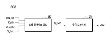
도 4를 참조하면, 일 실시예에 의한 입출력(IO) 회로(205)는 프리-엠퍼시스 회로(260) 및 출력 드라이버(270)를 포함할 수 있다.Referring to FIG. 4 , an input/output (IO)
프리-엠퍼시스 회로(260)는 송신 데이터(DIN_REF), 인에이블 신호(EQ_EN), 제 1 지연 제어 신호(DL_ZERO) 및 제 2 지연 제어 신호(DL_CAL)를 제공받을 수 있다. 프리-엠퍼시스 회로(260)는 인에이블 신호(EQ_EN)가 비활성화 상태인 경우, 제 1 지연 제어 신호(DL_ZETO)에 응답하여 지연되지 않은 송신 데이터(DIN_REF)를 송신 데이터(DIN_REF)와 결합하여 엠퍼시스 신호(D_EMP)를 생성할 수 있다. 인에이블 신호(EQ_EN)가 활성화 상태인 경우, 프리-엠퍼시스 회로(260)는 제 2 지연 제어 신호(DL_CAL)에 응답하여 송신 데이터(DIN_REF)를 지연 제어 신호(DL_CAL)에 해당하는 지연량(1UI)만큼 지연시켜 부가 신호를 생하고, 부가 신호를 송신 데이터(DIN_REF)에 결합하여 엠퍼시스 신호(D_EMP)를 생성할 수 있다.The
출력 드라이버(270)는 엠퍼시스 신호(D_EMP)를 구동하여 출력 패드(DOUT)에 데이터 신호를 인가하여 호스트 장치(100)로 전송할 수 있다.The
도시하지 않았지만, 출력 드라이버(270)는 임피던스 매칭 코드에 따라 온/오프되는 복수의 단위 드라이버(레그)를 포함할 수 있다.Although not shown, the
일 실시예에서, 프리 엠퍼시스 회로(260)는 출력 드라이버(270)와 통합될 수 있다. 이 경우 출력 드라이버(270)를 구성하는 복수의 단위 드라이버 중, 오프 상태의 드라이버를 프리-엠퍼시스 회로로 활용하면 프리-엠퍼시스 동작을 위한 별도의 회로를 추가할 필요가 없어 제 2 인터페이스 회로(220)의 사이즈를 감소시킬 수 있다.In one embodiment, the
도 5는 일 실시예에 의한 프리-엠퍼시스 회로의 구성도이다.5 is a block diagram of a pre-emphasis circuit according to an embodiment.
도 5를 참조하면, 일 실시예에 의한 프리-엠퍼시스 회로(260)는 제 1 선택부(216), 제 2 선택부(263), 제 1 지연부(265), 제 2 지연부(267), 제 1 구동부(2691) 및 제 2 구동부(2693)를 포함할 수 있다.Referring to FIG. 5 , the
제 1 지연부(265)는 무지연 회로로서, 송신 데이터(DIN_REF)를 제공받아 지연시키지 않고 소스 데이터(DIN)로 출력하도록 구성될 수 있다.The
제 1 선택부(261)는 인에이블 신호(EQ_EN)에 응답하여 송신 데이터(DIN_REF)와 그 반전 신호 중 어느 하나를 선택하여 제 2 지연부(267)로 제공하도록 도록 구성될 수 있다. 일 실시예에서, 제 1 선택부(261)는 인에이블 신호(EQ_EN)가 비활성화 상태인 경우에는 송신 데이터(DIN_REF)를 선택하고, 인에이블 신호(EQ_EN)가 활성화 상태인 경우에는 반전된 송신 데이터(DIN_REF)를 선택하도록 구성될 수 있다.The
제 2 선택부(263)는 인에이블 신호(EQ_EN)에 응답하여, 제 1 지연 제어 신호(DL_ZERO) 및 제 2 지연 제어 신호(DL_CAL) 중 어느 하나를 선택하여 제 2 지연부(267)로 제공할 수 있다. 일 실시예에서, 제 1 선택부(261)는 인에이블 신호(EQ_EN)가 비활성화 상태인 경우에는 지연량이 0인 제 1 지연 제어 신호(DL_ZERO)를 선택하고, 인에이블 신호(EQ_EN)가 활성화 상태인 경우에는 지연량이 1UI인 제 2 지연 제어 신호(DL_CAL)를 선택하도록 구성될 수 있다.The
제 2 지연부(267)는 제 2 선택부(263)로부터 제공되는 제 1 지연 제어 신호(DL_ZERO) 또는 제 2 지연 제어 신호(DL_CAL)에 기초하여 제 1 선택부(261)로부터 제공되는 신호, 즉 송신 데이터(DIN_REF) 또는 그 반전 신호를 지연시켜 부가 신호(DIN_ZM)를 생성할 수 있다.The
제 1 구동부(2691)는 제 1 지연부(265)로부터 제공되는 소스 데이터(DIN)를 증폭하여 출력할 수 있다. 제 2 구동부(2693)는 부가 신호(DIN_ZM)를 구동하고 소스 신호(DIN)에 결합하여 엠퍼시스 신호(D_EMP)를 출력할 수 있다.The
제 2 지연 제어 신호(DL_CAL)가 입출력 제어 회로(20) 내에 구비된 DLL 회로(201)로부터 생성되어 각각의 IO 회로(205)로 제공됨에 따라, 별도의 지연 회로를 추가하지 않고도 PVT 변동에 의존하지 않는 부가 신호를 생성할 수 있다.As the second delay control signal DL_CAL is generated from the
따라서, 지연 회로를 위한 면적의 낭비 없이 데이터의 무결성을 보장할 수 있다.Accordingly, data integrity can be ensured without wasting an area for the delay circuit.
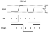
도 6A 및 도 6B는 프리-엠퍼시스 여부에 따른 송신 신호의 파형도이다.6A and 6B are waveform diagrams of a transmission signal according to whether pre-emphasis is applied.
도 6A는 프리-엠퍼시스를 수행하지 않은 경우, 즉 인에이블 신호(EQ_EN)가 비활성화 상태인 경우의 송신 신호에 대한 파형도이다.6A is a waveform diagram of a transmission signal when pre-emphasis is not performed, that is, when the enable signal EQ_EN is in an inactive state.
인에이블 신호(EQ_EN)가 비활성화 상태이므로 제 1 선택부(261)는 반전되지 않은 송신 데이터(DIN_REF)를 출력하고, 제 2 선택부(263)는 제 1 지연 제어 신호(DL_ZERO)를 선택하여 출력한다. 제 1 지연 제어 신호(DL_ZERO)는 지연량을 0으로 하는 신호이므로, 제 2 지연부(267)로부터는 제 1 지연부(265)에서 출력되는 소스 데이터(DIN)와 위상 및 논리 레벨이 동일한 부가 신호(DIN_ZM)가 출력된다.Since the enable signal EQ_EN is in an inactive state, the
소스 데이터(DIN)는 제 1 구동부(2691)에서 구동되고, 부가 신호(DIN_ZM)는 제 2 구동부(2693)에서 구동되어, 소스 신호(DIN)의 하이 레벨(VH) 및 로우 레벨(VL)이 각각 VCCQ 및 VSSQ로 강화된 엠퍼시스 신호(D_EMP)가 출력될 수 있다.The source data DIN is driven by the
도 6B는 프리-엠퍼시스를 수행한 경우, 즉 인에이블 신호(EQ_EN)가 활성화 상태인 경우의 송신 데이터에 대한 파형도이다.6B is a waveform diagram of transmission data when pre-emphasis is performed, that is, when the enable signal EQ_EN is in an active state.
인에이블 신호(EQ_EN)가 활성화 상태이므로 제 1 선택부(261)는 반전된 송신 데이터(DIN_REF)를 출력하고, 제 2 선택부(263)는 제 2 지연 제어 신호(DL_CAL)를 선택하여 출력한다. 제 2 지연 제어 신호(DL_CAL)는 지연량을 1UI로 하는 신호이므로, 제 2 지연부(267)는 반전된 송신 데이터(DIN_REF)를 1UI 지연하여, 소스 데이터(DIN)보다 1UI 지연된 부가 신호(DIN_ZM)가 출력된다.Since the enable signal EQ_EN is activated, the
소스 데이터(DIN)는 제 1 구동부(2691)에서 구동되고, 부가 신호(DIN_ZM)는 제 2 구동부(2693)에서 구동되어, 소스 신호(DIN)와 부가 신호(DIN_ZM)의 하이 레벨(VH)이 중첩되는 구간 및 로우 레벨(VL)이 중첩되는 구간, 즉 소스 신호(DIN)의 논리 레벨이 천이되는 시점에 각각 VCCQ 및 VSSQ로 강화된 엠퍼시스 신호(D_EMP)가 출력될 수 있다.The source data DIN is driven by the
소스 데이터(DIN)의 비트값이 토글하는 고주파 구간에서 부가 신호에 의해 송신 신호를 강조함으로써 채널을 경유하여 전송되는 송신 신호가 감쇄되는 것을 방지할 수 있다.By emphasizing the transmission signal by the additional signal in the high frequency section in which the bit value of the source data DIN toggles, it is possible to prevent the transmission signal transmitted through the channel from being attenuated.
도 7은 일 실시예에 의한 스토리지 시스템의 구성도이다.7 is a configuration diagram of a storage system according to an exemplary embodiment.
도 7을 참조하면, 스토리지 시스템(1000)은 호스트 장치(1100)와 데이터 저장 장치(1200)를 포함할 수 있다. 일 실시예에서, 데이터 저장 장치(1200)는 솔리드 스테이트 드라이브(solid state drive)(SSD)로 구성될 수 있다.Referring to FIG. 7 , the
데이터 저장 장치(1200)는 컨트롤러(1210), 비휘발성 메모리 장치들(1220-0 ~ 1220-n), 버퍼 메모리 장치(1230), 전원 공급기(1240), 신호 커넥터(1101) 및 전원 커넥터(1103)를 포함할 수 있다.The
컨트롤러(1210)는 데이터 저장 장치(1200)의 제반 동작을 제어할 수 있다. 컨트롤러(1210)는 호스트 인터페이스 유닛, 컨트롤 유닛, 동작 메모리로서의 랜덤 액세스 메모리, 에러 정정 코드(ECC) 유닛 및 메모리 인터페이스 유닛을 포함할 수 있다. 예를 들어, 데이터 저장 장치(1200)는 도 2 내지 도 5에 도시한 인터페이스 회로를 포함할 수 있다.The
호스트 장치(1100)와 데이터 저장 장치(1200)는 신호 커넥터(1101)를 통해 신호를 송수신할 수 있다. 여기에서, 신호란 명령어, 어드레스, 데이터를 포함할 수 있다.The
컨트롤러(1210)는 호스트 장치(1100)로부터 입력된 신호를 분석하고 처리할 수 있다. 컨트롤러(1210)는 데이터 저장 장치(1200)를 구동하기 위한 펌웨어 또는 소프트웨어에 따라서 백그라운드 기능 블럭들의 동작을 제어할 수 있다The
버퍼 메모리 장치(1230)는 비휘발성 메모리 장치들(1220-0 ~ 1220-n)에 저장될 데이터를 임시 저장할 수 있다. 또한, 버퍼 메모리 장치(1230)는 비휘발성 메모리 장치들(1220-0 ~ 1220-n)로부터 읽혀진 데이터를 임시 저장할 수 있다. 버퍼 메모리 장치(1230)에 임시 저장된 데이터는 컨트롤러(1210)의 제어에 따라 호스트 장치(1100) 또는 비휘발성 메모리 장치들(1220-0 ~ 1220-n)로 전송될 수 있다.The
비휘발성 메모리 장치들(1220-0 ~ 1220-n)은 데이터 저장 장치(1200)의 저장 매체로 사용될 수 있다. 비휘발성 메모리 장치들(1220-0 ~ 1220-n) 각각은 복수의 채널들(CH0~CHn)을 통해 컨트롤러(1210)와 연결될 수 있다. 하나의 채널에는 하나 또는 그 이상의 비휘발성 메모리 장치가 연결될 수 있다. 하나의 채널에 연결되는 비휘발성 메모리 장치들은 동일한 신호 버스 및 데이터 버스에 연결될 수 있다.The nonvolatile memory devices 1220 - 0 to 1220 - n may be used as storage media of the
전원 공급기(1240)는 전원 커넥터(1103)를 통해 입력된 전원을 데이터 저장 장치(1200)에 제공할 수 있다. 전원 공급기(1240)는 보조 전원 공급기(1241)를 포함할 수 있다. 보조 전원 공급기(1241)는 서든 파워 오프(sudden power off)가 발생되는 경우, 데이터 저장 장치(1200)가 정상적으로 종료될 수 있도록 전원을 공급할 수 있다. 보조 전원 공급기(1241)는 대용량 캐패시터들(capacitors)을 포함할 수 있으나 이에 한정되는 것은 아니다.The
신호 커넥터(1101)는 호스트 장치(1100)와 데이터 저장 장치(1200)의 인터페이스 방식에 따라서 다양한 형태의 커넥터로 구성될 수 있음은 자명하다.It is obvious that the
전원 커넥터(1103)는 호스트 장치(1100)의 전원 공급 방식에 따라서 다양한 형태의 커넥터로 구성될 수 있음은 물론이다.Of course, the
도 8 및 도 9는 실시예들에 따른 데이터 처리 시스템의 구성도이다.8 and 9 are block diagrams of data processing systems according to embodiments.
도 8을 참조하면, 데이터 처리 시스템(3000)은 호스트 장치(3100)와 메모리 시스템(3200)을 포함할 수 있다.Referring to FIG. 8 , the
호스트 장치(3100)는 인쇄 회로 기판(printed circuit board)과 같은 기판(board) 형태로 구성될 수 있다. 비록 도시되지 않았지만, 호스트 장치(3100)는 호스트 장치의 기능을 수행하기 위한 백그라운드 기능 블럭들을 포함할 수 있다.The
호스트 장치(3100)는 소켓(socket), 슬롯(slot) 또는 커넥터(connector)와 같은 접속 터미널(3110)을 포함할 수 있다. 메모리 시스템(3200)은 접속 터미널(3110)에 마운트(mount)될 수 있다.The
메모리 시스템(3200)은 인쇄 회로 기판과 같은 기판 형태로 구성될 수 있다. 메모리 시스템(3200)은 메모리 모듈 또는 메모리 카드로 불릴 수 있다. 메모리 시스템(3200)은 컨트롤러(3210), 버퍼 메모리 장치(3220), 비휘발성 메모리 장치(3231~3232), PMIC(power management integrated circuit)(3240) 및 접속 터미널(3250)을 포함할 수 있다.The
컨트롤러(3210)는 메모리 시스템(3200)의 제반 동작을 제어할 수 있다.The
메모리 시스템(3200)은 도 2 내지 도 5에 도시한 인터페이스 회로를 포함할 수 있다.The
버퍼 메모리 장치(3220)는 비휘발성 메모리 장치들(3231~3232)에 저장될 데이터를 임시 저장할 수 있다. 또한, 버퍼 메모리 장치(3220)는 비휘발성 메모리 장치들(3231~3232)로부터 읽혀진 데이터를 임시 저장할 수 있다. 버퍼 메모리 장치(3220)에 임시 저장된 데이터는 컨트롤러(3210)의 제어에 따라 호스트 장치(3100) 또는 비휘발성 메모리 장치들(3231~3232)로 전송될 수 있다.The
비휘발성 메모리 장치들(3231~3232)은 메모리 시스템(3200)의 저장 매체로 사용될 수 있다.The
PMIC(3240)는 접속 터미널(3250)을 통해 입력된 전원을 메모리 시스템(3200) 백그라운드에 제공할 수 있다. PMIC(3240)는, 컨트롤러(3210)의 제어에 따라서, 메모리 시스템(3200)의 전원을 관리할 수 있다.The
접속 터미널(3250)은 호스트 장치의 접속 터미널(3110)에 연결될 수 있다. 접속 터미널(3250)을 통해서, 호스트 장치(3100)와 메모리 시스템(3200) 간에 커맨드, 어드레스, 데이터 등과 같은 신호와, 전원이 전달될 수 있다. 접속 터미널(3250)은 호스트 장치(3100)와 메모리 시스템(3200)의 인터페이스 방식에 따라 다양한 형태로 구성될 수 있다. 접속 터미널(3250)은 메모리 시스템(3200)의 어느 한 변에 배치될 수 있다.The
도 9는 본 발명의 실시 예에 따른 메모리 시스템을 포함하는 데이터 처리 시스템을 예시적으로 도시하는 도면이다.9 is a diagram exemplarily illustrating a data processing system including a memory system according to an embodiment of the present invention.
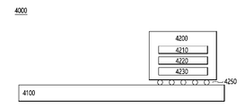
도 9를 참조하면, 데이터 처리 시스템(4000)은 호스트 장치(4100)와 메모리 시스템(4200)을 포함할 수 있다.Referring to FIG. 9 , the
호스트 장치(4100)는 인쇄 회로 기판(printed circuit board)과 같은 기판(board) 형태로 구성될 수 있다. 비록 도시되지 않았지만, 호스트 장치(4100)는 호스트 장치의 기능을 수행하기 위한 백그라운드 기능 블럭들을 포함할 수 있다.The
메모리 시스템(4200)은 표면 실장형 패키지 형태로 구성될 수 있다. 메모리 시스템(4200)은 솔더 볼(solder ball)(4250)을 통해서 호스트 장치(4100)에 마운트될 수 있다. 메모리 시스템(4200)은 컨트롤러(4210), 버퍼 메모리 장치(4220) 및 비휘발성 메모리 장치(4230)를 포함할 수 있다.The
컨트롤러(4210)는 메모리 시스템(4200)의 제반 동작을 제어할 수 있다. 메모리 시스템(4200)은 도 2 내지 도 5에 도시한 인터페이스 회로를 포함할 수 있다.The
버퍼 메모리 장치(4220)는 비휘발성 메모리 장치(4230)에 저장될 데이터를 임시 저장할 수 있다. 또한, 버퍼 메모리 장치(4220)는 비휘발성 메모리 장치들(4230)로부터 읽혀진 데이터를 임시 저장할 수 있다. 버퍼 메모리 장치(4220)에 임시 저장된 데이터는 컨트롤러(4210)의 제어에 따라 호스트 장치(4100) 또는 비휘발성 메모리 장치(4230)로 전송될 수 있다.The
비휘발성 메모리 장치(4230)는 메모리 시스템(4200)의 저장 매체로 사용될 수 있다.The
도 10은 일 실시예에 의한 데이터 저장 장치를 포함하는 네트워크 시스템의 구성도이다.10 is a block diagram of a network system including a data storage device according to an embodiment.
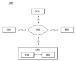
도 10을 참조하면, 네트워크 시스템(5000)은 네트워크(5500)를 통해서 연결된 서버 시스템(5300) 및 복수의 클라이언트 시스템들(5410~5430)을 포함할 수 있다.Referring to FIG. 10 , a
서버 시스템(5300)은 복수의 클라이언트 시스템들(5410~5430)의 요청에 응답하여 데이터를 서비스할 수 있다. 예를 들면, 서버 시스템(5300)은 복수의 클라이언트 시스템들(5410~5430)로부터 제공된 데이터를 저장할 수 있다. 다른 예로서, 서버 시스템(5300)은 복수의 클라이언트 시스템들(5410~5430)로 데이터를 제공할 수 있다.The
서버 시스템(5300)은 호스트 장치(5100) 및 메모리 시스템(5200)을 포함할 수 있다. 메모리 시스템(5200)은 도 1 내지 도 5의 데이터 저장 장치(10), 도 7의 데이터 저장 장치(1200), 도 8의 메모리 시스템(3200), 도 9의 메모리 시스템(4200)으로 구성될 수 있다.The
도 11은 일 실시 예에 따른 데이터 저장 장치에 포함된 비휘발성 메모리 장치의 구성도이다.11 is a block diagram of a nonvolatile memory device included in a data storage device according to an exemplary embodiment.
도 11을 참조하면, 비휘발성 메모리 장치(300)는 메모리 셀 어레이(310), 행 디코더(320), 데이터 읽기/쓰기 블럭(330), 열 디코더(340), 전압 발생기(350) 및 제어 로직(360)을 포함할 수 있다. Referring to FIG. 11 , the
메모리 셀 어레이(310)는 워드 라인들(WL1~WLm)과 비트 라인들(BL1~BLn)이 서로 교차된 영역에 배열된 메모리 셀(MC)들을 포함할 수 있다.The
메모리 셀 어레이(310)는 3차원 메모리 어레이를 포함할 수 있다. 3차원 메모리 어레이는 반도체 기판의 평판면에 대해 수직의 방향성을 가지며, 적어도 하나의 메모리 셀이 다른 하나의 메모리 셀의 수직 상부에 위치하는 낸드(NAND) 스트링을 포함하는 구조를 의미한다. 하지만 3차원 메모리 어레이의 구조가 이에 한정되는 것은 아니며 수직의 방향성뿐 아니라 수평의 방향성을 가지고 고집적도로 형성된 메모리 어레이 구조라면 선택적으로 적용 가능함은 자명하다.The
행 디코더(320)는 워드 라인들(WL1~WLm)을 통해서 메모리 셀 어레이(310)와 연결될 수 있다. 행 디코더(320)는 제어 로직(360)의 제어에 따라 동작할 수 있다. 행 디코더(320)는 외부 장치(도시되지 않음)로부터 제공된 어드레스를 디코딩할 수 있다. 행 디코더(320)는 디코딩 결과에 근거하여 워드 라인들(WL1~WLm)을 선택하고, 구동할 수 있다. 예시적으로, 행 디코더(320)는 전압 발생기(350)로부터 제공된 워드 라인 전압을 워드 라인들(WL1~WLm)에 제공할 수 있다.The
데이터 읽기/쓰기 블럭(330)은 비트 라인들(BL1~BLn)을 통해서 메모리 셀 어레이(310)와 연결될 수 있다. 데이터 읽기/쓰기 블럭(330)은 비트 라인들(BL1~BLn) 각각에 대응하는 읽기/쓰기 회로들(RW1~RWn)을 포함할 수 있다. 데이터 읽기/쓰기 블럭(330)은 제어 로직(360)의 제어에 따라 동작할 수 있다. 데이터 읽기/쓰기 블럭(330)은 동작 모드에 따라서 쓰기 드라이버로서 또는 감지 증폭기로서 동작할 수 있다. 예를 들면, 데이터 읽기/쓰기 블럭(330)은 쓰기 동작 시 외부 장치로부터 제공된 데이터를 메모리 셀 어레이(310)에 저장하는 쓰기 드라이버로서 동작할 수 있다. 다른 예로서, 데이터 읽기/쓰기 블럭(330)은 읽기 동작 시 메모리 셀 어레이(310)로부터 데이터를 독출하는 감지 증폭기로서 동작할 수 있다.The data read/
열 디코더(340)는 제어 로직(360)의 제어에 따라 동작할 수 있다. 열 디코더(340)는 외부 장치로부터 제공된 어드레스를 디코딩할 수 있다. 열 디코더(340)는 디코딩 결과에 근거하여 비트 라인들(BL1~BLn) 각각에 대응하는 데이터 읽기/쓰기 블럭(330)의 읽기/쓰기 회로들(RW1~RWn)과 데이터 입출력 라인(또는 데이터 입출력 버퍼)을 연결할 수 있다.The
전압 발생기(350)는 비휘발성 메모리 장치(300)의 백그라운드 동작에 사용되는 전압을 생성할 수 있다. 전압 발생기(350)에 의해서 생성된 전압들은 메모리 셀 어레이(310)의 메모리 셀들에 인가될 수 있다. 예를 들면, 프로그램 동작 시 생성된 프로그램 전압은 프로그램 동작이 수행될 메모리 셀들의 워드 라인에 인가될 수 있다. 다른 예로서, 소거 동작 시 생성된 소거 전압은 소거 동작이 수행될 메모리 셀들의 웰-영역에 인가될 수 있다. 다른 예로서, 읽기 동작 시 생성된 읽기 전압은 읽기 동작이 수행될 메모리 셀들의 워드 라인에 인가될 수 있다.The
제어 로직(360)은 외부 장치로부터 제공된 제어 신호에 근거하여 비휘발성 메모리 장치(300)의 제반 동작을 제어할 수 있다. 예를 들면, 제어 로직(360)은 비휘발성 메모리 장치(300)의 읽기, 쓰기, 소거 동작을 제어할 수 있다.The
이와 같이, 본 발명이 속하는 기술분야의 당업자는 본 발명이 그 기술적 사상이나 필수적 특징을 변경하지 않고서 다른 구체적인 형태로 실시될 수 있다는 것을 이해할 수 있을 것이다. 그러므로 이상에서 기술한 실시예들은 모든 면에서 예시적인 것이며 한정적인 것이 아닌 것으로서 이해해야만 한다. 본 발명의 범위는 상기 상세한 설명보다는 후술하는 특허청구범위에 의하여 나타내어지며, 특허청구범위의 의미 및 범위 그리고 그 등가개념으로부터 도출되는 모든 변경 또는 변형된 형태가 본 발명의 범위에 포함되는 것으로 해석되어야 한다.As such, those skilled in the art to which the present invention pertains will understand that the present invention may be embodied in other specific forms without changing the technical spirit or essential characteristics thereof. Therefore, it should be understood that the embodiments described above are illustrative in all respects and not restrictive. The scope of the present invention is indicated by the following claims rather than the above detailed description, and all changes or modifications derived from the meaning and scope of the claims and their equivalent concepts should be interpreted as being included in the scope of the present invention. do.
10 : 데이터 저장 장치
100 : 호스트 장치
110 : 메모리 컨트롤러
120 : 제 1 인터페이스 회로
200 : 저장
210 : 메모리 장치
220 : 제 2 인터페이스 회로10: data storage device
100: host device
110: memory controller
120: first interface circuit
200 : save
210: memory device
220: second interface circuit
Claims (16)
상기 호스트 장치와 인터페이스 회로를 통해 통신하는 메모리 장치를 포함하고,
상기 인터페이스 회로는 지연고정루프 회로에서 생성한 지연코드에 기초하여 상기 호스트 장치로 전송할 송신 신호에 결합할 부가 신호를 생성하도록 구성되는 데이터 저장 장치.a host device including a memory controller; and
a memory device communicating with the host device through an interface circuit;
and the interface circuit is configured to generate an additional signal to be coupled to a transmission signal to be transmitted to the host device based on the delay code generated by the delay locked loop circuit.
상기 인터페이스 회로는 상기 지연고정루프 회로; 및
상기 지연코드에 기초하여 결정된 지연시간만큼 상기 송신 신호를 지연시켜 상기 부가 신호를 생성하고, 상기 송신 신호와 상기 부가 신호를 결합하도록 구성되는 프리-엠퍼시스 회로;
를 포함하도록 구성되는 데이터 저장 장치.The method of claim 1,
The interface circuit may include the delay locked loop circuit; and
a pre-emphasis circuit configured to delay the transmission signal by a delay time determined based on the delay code to generate the additional signal, and to combine the transmission signal and the additional signal;
A data storage device configured to include
상기 지연시간은 상기 송신 신호의 1UI(Unit Interval)에 대응하는 데이터 저장 장치.3. The method of claim 2,
The delay time is a data storage device corresponding to 1 UI (Unit Interval) of the transmission signal.
상기 인터페이스 회로는, 상기 프리-엠퍼시스 회로를 각각 구비하는 복수의 입출력 회로를 포함하고,
상기 지연고정루프 회로는 상기 복수의 입출력 회로와 함께 집적되는 데이터 저장 장치.3. The method of claim 2,
The interface circuit includes a plurality of input/output circuits each having the pre-emphasis circuit,
wherein the delay locked loop circuit is integrated together with the plurality of input/output circuits.
상기 지연고정루프 회로는 파워-업 후 듀티 사이클 보정에 사용되는 클럭 신호에 기초하여 상기 지연코드를 생성하도록 구성되는 데이터 저장 장치.The method of claim 1,
and the delay locked loop circuit is configured to generate the delay code based on a clock signal used for duty cycle correction after power-up.
상기 인터페이스 회로는, 복수의 입출력 회로를 포함하고,
상기 지연코드는 상기 복수의 입출력 회로 각각으로 제공되는 데이터 저장 장치.The method of claim 1,
The interface circuit includes a plurality of input/output circuits,
The delay code is provided to each of the plurality of input/output circuits.
상기 인터페이스 회로를 통해 호스트 장치와 데이터를 송수신하는 메모리 장치;를 포함하고,
상기 입출력 제어 회로는, 상기 호스트 장치로부터 전송되는 클럭 신호에 기초하여 내부 클럭신호 및 지연 코드를 생성하는 지연고정루프 회로; 및
상기 지연코드를 수신하여 상기 호스트 장치로 전송할 송신 신호에 결합할 부가 신호를 생성하도록 구성되는 복수의 입출력 회로;
를 포함하도록 구성되는 데이터 저장 장치.an interface circuit including an input/output control circuit; and
a memory device that transmits and receives data to and from a host device through the interface circuit;
The input/output control circuit may include a delay locked loop circuit configured to generate an internal clock signal and a delay code based on a clock signal transmitted from the host device; and
a plurality of input/output circuits configured to receive the delay code and generate an additional signal to be coupled to a transmission signal to be transmitted to the host device;
A data storage device configured to include
상기 복수의 입출력 회로 각각은, 상기 지연코드에 기초하여 결정된 지연시간만큼 상기 송신 신호를 지연시켜 상기 부가 신호를 생성하도록 구성되는 프리-엠퍼시스 회로를 포함하도록 구성되는 데이터 저장 장치.8. The method of claim 7,
and each of the plurality of input/output circuits includes a pre-emphasis circuit configured to generate the additional signal by delaying the transmission signal by a delay time determined based on the delay code.
상기 지연시간은 상기 송신 신호의 1UI(Unit Interval)에 대응하는 데이터 저장 장치.9. The method of claim 8,
The delay time is a data storage device corresponding to 1 UI (Unit Interval) of the transmission signal.
상기 지연고정루프 회로는 상기 복수의 입출력 회로와 함께 집적되는 데이터 저장 장치.8. The method of claim 7,
wherein the delay locked loop circuit is integrated together with the plurality of input/output circuits.
상기 지연고정루프 회로는 파워-업 후 듀티 사이클 보정에 사용되는 클럭 신호에 기초하여 상기 지연코드를 생성하도록 구성되는 데이터 저장 장치.8. The method of claim 7,
and the delay locked loop circuit is configured to generate the delay code based on a clock signal used for duty cycle correction after power-up.
호스트 장치로부터 전송되는 클럭 신호에 기초하여 내부 클럭신호 및 지연코드를 생성하는 지연고정루프 회로; 및
상기 지연코드를 수신하여 상기 호스트 장치로 전송할 송신 신호에 결합할 부가 신호를 생성하도록 구성되는 복수의 입출력 회로;
를 포함하도록 구성되는 인터페이스 회로.An interface circuit provided in a storage unit including a memory device, comprising:
a delay locked loop circuit that generates an internal clock signal and a delay code based on a clock signal transmitted from a host device; and
a plurality of input/output circuits configured to receive the delay code and generate an additional signal to be coupled to a transmission signal to be transmitted to the host device;
An interface circuit configured to include a.
상기 복수의 입출력 회로 각각은, 상기 지연코드에 기초하여 결정된 지연시간만큼 상기 송신 신호를 지연시켜 상기 부가 신호를 생성하도록 구성되는 프리-엠퍼시스 회로를 포함하도록 구성되는 인터페이스 회로.13. The method of claim 12,
and each of the plurality of input/output circuits includes a pre-emphasis circuit configured to generate the additional signal by delaying the transmission signal by a delay time determined based on the delay code.
상기 지연시간은 상기 송신 신호의 1UI(Unit Interval)에 대응하는 인터페이스 회로.14. The method of claim 13,
The delay time is an interface circuit corresponding to 1 UI (Unit Interval) of the transmission signal.
상기 지연고정루프회로는 상기 복수의 입출력 회로와 함께 집적되는 인터페이스 회로.13. The method of claim 12,
The delay locked loop circuit is an interface circuit integrated together with the plurality of input/output circuits.
상기 인터페이스 회로는 파워-업 동작 후 듀티 사이클 보정에 사용되는 클럭 신호에 기초하여 상기 지연코드를 생성하도록 구성되는 인터페이스 회로.13. The method of claim 12,
and the interface circuit is configured to generate the delay code based on a clock signal used for duty cycle correction after a power-up operation.
Priority Applications (3)
| Application Number | Priority Date | Filing Date | Title |
|---|---|---|---|
| KR1020210032790A KR102915284B1 (en) | 2021-03-12 | 2021-03-12 | Data Storage Apparatus and Interface Circuit Therefor |
| US17/393,001 US11704051B2 (en) | 2021-03-12 | 2021-08-03 | Data storage apparatus and interface circuit therefor |
| CN202111323388.5A CN115083458A (en) | 2021-03-12 | 2021-11-08 | Data storage device and interface circuit thereof |
Applications Claiming Priority (1)
| Application Number | Priority Date | Filing Date | Title |
|---|---|---|---|
| KR1020210032790A KR102915284B1 (en) | 2021-03-12 | 2021-03-12 | Data Storage Apparatus and Interface Circuit Therefor |
Publications (2)
| Publication Number | Publication Date |
|---|---|
| KR20220128126A true KR20220128126A (en) | 2022-09-20 |
| KR102915284B1 KR102915284B1 (en) | 2026-01-22 |
Family
ID=83193803
Family Applications (1)
| Application Number | Title | Priority Date | Filing Date |
|---|---|---|---|
| KR1020210032790A Active KR102915284B1 (en) | 2021-03-12 | 2021-03-12 | Data Storage Apparatus and Interface Circuit Therefor |
Country Status (3)
| Country | Link |
|---|---|
| US (1) | US11704051B2 (en) |
| KR (1) | KR102915284B1 (en) |
| CN (1) | CN115083458A (en) |
Cited By (1)
| Publication number | Priority date | Publication date | Assignee | Title |
|---|---|---|---|---|
| KR102730366B1 (en) * | 2023-06-27 | 2024-11-14 | 주식회사 엑시콘 | Test Apparatus And Method For Signal Synchronization |
Families Citing this family (3)
| Publication number | Priority date | Publication date | Assignee | Title |
|---|---|---|---|---|
| US12206530B2 (en) * | 2022-01-06 | 2025-01-21 | Brookhaven Science Associates, Llc | User-configurable high-speed line driver |
| US12175118B2 (en) * | 2022-03-22 | 2024-12-24 | Silicon Laboratories Inc. | External nonvolatile memory with additional functionality |
| JP7655975B2 (en) * | 2023-07-13 | 2025-04-02 | レノボ・シンガポール・プライベート・リミテッド | Information processing device and control method |
Family Cites Families (10)
| Publication number | Priority date | Publication date | Assignee | Title |
|---|---|---|---|---|
| US7440340B2 (en) * | 2004-10-19 | 2008-10-21 | Samsung Electronics Co., Ltd. | Output buffer of a semiconductor memory device |
| KR100695002B1 (en) * | 2005-09-15 | 2007-03-13 | 주식회사 하이닉스반도체 | Dl with auto reset |
| KR100862233B1 (en) | 2007-01-04 | 2008-10-09 | 한국과학기술원 | Pre-emphasis output circuit with tap delay line with variable delay time |
| KR101045071B1 (en) | 2009-11-30 | 2011-06-29 | 주식회사 하이닉스반도체 | Data output circuit |
| US8760188B2 (en) * | 2011-06-30 | 2014-06-24 | Silicon Image, Inc. | Configurable multi-dimensional driver and receiver |
| KR20150134002A (en) | 2014-05-21 | 2015-12-01 | 에스케이하이닉스 주식회사 | Semiconductor device |
| US9971733B1 (en) | 2014-12-04 | 2018-05-15 | Altera Corporation | Scalable 2.5D interface circuitry |
| US10528515B2 (en) * | 2017-06-27 | 2020-01-07 | Intel Corporation | Memory channel driver with echo cancellation |
| US10530617B2 (en) | 2017-08-07 | 2020-01-07 | Micron Technology, Inc. | Programmable channel equalization for multi-level signaling |
| KR20190051314A (en) | 2017-11-06 | 2019-05-15 | 삼성전자주식회사 | Electronic circuit for ouputting post emphasis signal |
-
2021
- 2021-03-12 KR KR1020210032790A patent/KR102915284B1/en active Active
- 2021-08-03 US US17/393,001 patent/US11704051B2/en active Active
- 2021-11-08 CN CN202111323388.5A patent/CN115083458A/en active Pending
Cited By (1)
| Publication number | Priority date | Publication date | Assignee | Title |
|---|---|---|---|---|
| KR102730366B1 (en) * | 2023-06-27 | 2024-11-14 | 주식회사 엑시콘 | Test Apparatus And Method For Signal Synchronization |
Also Published As
| Publication number | Publication date |
|---|---|
| US20220291863A1 (en) | 2022-09-15 |
| US11704051B2 (en) | 2023-07-18 |
| CN115083458A (en) | 2022-09-20 |
| KR102915284B1 (en) | 2026-01-22 |
Similar Documents
| Publication | Publication Date | Title |
|---|---|---|
| US11500770B2 (en) | Memory device controlling including reading from a first memory and writing to a second memory based on timing and control signals | |
| KR102915284B1 (en) | Data Storage Apparatus and Interface Circuit Therefor | |
| US9971521B2 (en) | Memory devices, systems and methods employing command/address calibration | |
| US10133284B2 (en) | Circuits for setting reference voltages and semiconductor devices including the same | |
| US10068633B2 (en) | Semiconductor devices and integrated circuits including the same | |
| KR20190120526A (en) | Memory device and operation method of the same | |
| US20250370869A1 (en) | Soft read operations with progressive data output | |
| KR102805363B1 (en) | Memory controller including a interconnect circuit, and memory system | |
| US11036433B2 (en) | Memory controller, data storage device, and storage system having the same | |
| US20220294445A1 (en) | Computer system and interface circuit therefor | |
| CN113889161A (en) | Configuring multiple register clock drivers of a memory subsystem | |
| US11211112B2 (en) | Semiconductor devices controlling column operation of banks | |
| US12237037B2 (en) | Device of generating reference voltages for multi-level signaling and memory system including the same | |
| KR20220111487A (en) | Memory system |
Legal Events
| Date | Code | Title | Description |
|---|---|---|---|
| PA0109 | Patent application |
St.27 status event code: A-0-1-A10-A12-nap-PA0109 |
|
| PG1501 | Laying open of application |
St.27 status event code: A-1-1-Q10-Q12-nap-PG1501 |
|
| PA0201 | Request for examination |
St.27 status event code: A-1-2-D10-D11-exm-PA0201 |
|
| E902 | Notification of reason for refusal | ||
| PE0902 | Notice of grounds for rejection |
St.27 status event code: A-1-2-D10-D21-exm-PE0902 |
|
| P11-X000 | Amendment of application requested |
St.27 status event code: A-2-2-P10-P11-nap-X000 |
|
| E601 | Decision to refuse application | ||
| PE0601 | Decision on rejection of patent |
St.27 status event code: N-2-6-B10-B15-exm-PE0601 |
|
| E13 | Pre-grant limitation requested |
Free format text: ST27 STATUS EVENT CODE: A-2-3-E10-E13-LIM-X000 (AS PROVIDED BY THE NATIONAL OFFICE) |
|
| E13-X000 | Pre-grant limitation requested |
St.27 status event code: A-2-3-E10-E13-lim-X000 |
|
| P11 | Amendment of application requested |
Free format text: ST27 STATUS EVENT CODE: A-2-2-P10-P11-NAP-X000 (AS PROVIDED BY THE NATIONAL OFFICE) |
|
| P11-X000 | Amendment of application requested |
St.27 status event code: A-2-2-P10-P11-nap-X000 |
|
| F13 | Ip right granted in full following pre-grant review |
Free format text: ST27 STATUS EVENT CODE: A-3-4-F10-F13-REX-PX0701 (AS PROVIDED BY THE NATIONAL OFFICE) |
|
| PX0701 | Decision of registration after re-examination |
St.27 status event code: A-3-4-F10-F13-rex-PX0701 |
|
| PG1601 | Publication of registration |
St.27 status event code: A-4-4-Q10-Q13-nap-PG1601 |
|
| Q13 | Ip right document published |
Free format text: ST27 STATUS EVENT CODE: A-4-4-Q10-Q13-NAP-PG1601 (AS PROVIDED BY THE NATIONAL OFFICE) |