KR20200138305A - Storage and electronic devices - Google Patents
Storage and electronic devices Download PDFInfo
- Publication number
- KR20200138305A KR20200138305A KR1020207030843A KR20207030843A KR20200138305A KR 20200138305 A KR20200138305 A KR 20200138305A KR 1020207030843 A KR1020207030843 A KR 1020207030843A KR 20207030843 A KR20207030843 A KR 20207030843A KR 20200138305 A KR20200138305 A KR 20200138305A
- Authority
- KR
- South Korea
- Prior art keywords
- transistor
- oxide
- insulator
- conductor
- potential
- Prior art date
Links
- 238000003860 storage Methods 0.000 title claims abstract description 30
- 229910044991 metal oxide Inorganic materials 0.000 claims abstract description 94
- 150000004706 metal oxides Chemical class 0.000 claims abstract description 84
- 239000003990 capacitor Substances 0.000 claims abstract description 77
- 230000015572 biosynthetic process Effects 0.000 claims abstract description 60
- 230000006870 function Effects 0.000 claims description 172
- 239000004065 semiconductor Substances 0.000 claims description 151
- 238000000034 method Methods 0.000 claims description 35
- 239000011701 zinc Substances 0.000 claims description 25
- 229910052738 indium Inorganic materials 0.000 claims description 10
- APFVFJFRJDLVQX-UHFFFAOYSA-N indium atom Chemical compound [In] APFVFJFRJDLVQX-UHFFFAOYSA-N 0.000 claims description 10
- GYHNNYVSQQEPJS-UHFFFAOYSA-N Gallium Chemical compound [Ga] GYHNNYVSQQEPJS-UHFFFAOYSA-N 0.000 claims description 8
- 229910052733 gallium Inorganic materials 0.000 claims description 8
- HCHKCACWOHOZIP-UHFFFAOYSA-N Zinc Chemical compound [Zn] HCHKCACWOHOZIP-UHFFFAOYSA-N 0.000 claims description 5
- 229910052725 zinc Inorganic materials 0.000 claims description 5
- 230000014759 maintenance of location Effects 0.000 abstract description 25
- 239000004020 conductor Substances 0.000 description 436
- 239000012212 insulator Substances 0.000 description 415
- 239000010408 film Substances 0.000 description 150
- 229910052760 oxygen Inorganic materials 0.000 description 103
- QVGXLLKOCUKJST-UHFFFAOYSA-N atomic oxygen Chemical compound [O] QVGXLLKOCUKJST-UHFFFAOYSA-N 0.000 description 102
- 239000001301 oxygen Substances 0.000 description 102
- 239000001257 hydrogen Substances 0.000 description 94
- 229910052739 hydrogen Inorganic materials 0.000 description 94
- UFHFLCQGNIYNRP-UHFFFAOYSA-N Hydrogen Chemical compound [H][H] UFHFLCQGNIYNRP-UHFFFAOYSA-N 0.000 description 85
- 239000010410 layer Substances 0.000 description 83
- 239000000463 material Substances 0.000 description 70
- 239000012535 impurity Substances 0.000 description 63
- 230000004888 barrier function Effects 0.000 description 54
- 238000009792 diffusion process Methods 0.000 description 53
- 230000002829 reductive effect Effects 0.000 description 43
- 229910052782 aluminium Inorganic materials 0.000 description 38
- XAGFODPZIPBFFR-UHFFFAOYSA-N aluminium Chemical group [Al] XAGFODPZIPBFFR-UHFFFAOYSA-N 0.000 description 38
- 238000010586 diagram Methods 0.000 description 37
- VYPSYNLAJGMNEJ-UHFFFAOYSA-N Silicium dioxide Chemical compound O=[Si]=O VYPSYNLAJGMNEJ-UHFFFAOYSA-N 0.000 description 35
- 229910052814 silicon oxide Inorganic materials 0.000 description 35
- 229910052721 tungsten Inorganic materials 0.000 description 31
- 239000010937 tungsten Substances 0.000 description 31
- WFKWXMTUELFFGS-UHFFFAOYSA-N tungsten Chemical compound [W] WFKWXMTUELFFGS-UHFFFAOYSA-N 0.000 description 30
- XLYOFNOQVPJJNP-UHFFFAOYSA-N water Substances O XLYOFNOQVPJJNP-UHFFFAOYSA-N 0.000 description 29
- 229910001868 water Inorganic materials 0.000 description 29
- 125000004429 atom Chemical group 0.000 description 28
- XUIMIQQOPSSXEZ-UHFFFAOYSA-N Silicon Chemical compound [Si] XUIMIQQOPSSXEZ-UHFFFAOYSA-N 0.000 description 27
- 229910052710 silicon Inorganic materials 0.000 description 27
- 239000010703 silicon Substances 0.000 description 27
- IJGRMHOSHXDMSA-UHFFFAOYSA-N Atomic nitrogen Chemical compound N#N IJGRMHOSHXDMSA-UHFFFAOYSA-N 0.000 description 26
- RYGMFSIKBFXOCR-UHFFFAOYSA-N Copper Chemical group [Cu] RYGMFSIKBFXOCR-UHFFFAOYSA-N 0.000 description 24
- 229910052751 metal Inorganic materials 0.000 description 23
- TWNQGVIAIRXVLR-UHFFFAOYSA-N oxo(oxoalumanyloxy)alumane Chemical compound O=[Al]O[Al]=O TWNQGVIAIRXVLR-UHFFFAOYSA-N 0.000 description 23
- 229910052581 Si3N4 Inorganic materials 0.000 description 22
- HQVNEWCFYHHQES-UHFFFAOYSA-N silicon nitride Chemical compound N12[Si]34N5[Si]62N3[Si]51N64 HQVNEWCFYHHQES-UHFFFAOYSA-N 0.000 description 22
- 239000000758 substrate Substances 0.000 description 22
- 239000002184 metal Substances 0.000 description 21
- PXHVJJICTQNCMI-UHFFFAOYSA-N Nickel Chemical group [Ni] PXHVJJICTQNCMI-UHFFFAOYSA-N 0.000 description 20
- RTAQQCXQSZGOHL-UHFFFAOYSA-N Titanium Chemical group [Ti] RTAQQCXQSZGOHL-UHFFFAOYSA-N 0.000 description 20
- 239000010949 copper Chemical group 0.000 description 20
- 229910052735 hafnium Inorganic materials 0.000 description 20
- 229910052719 titanium Inorganic materials 0.000 description 20
- 239000010936 titanium Chemical group 0.000 description 20
- 229910052802 copper Inorganic materials 0.000 description 19
- 230000007423 decrease Effects 0.000 description 18
- 230000005684 electric field Effects 0.000 description 17
- 230000003647 oxidation Effects 0.000 description 17
- 238000007254 oxidation reaction Methods 0.000 description 17
- 239000013078 crystal Substances 0.000 description 16
- 239000002356 single layer Substances 0.000 description 16
- 239000010409 thin film Substances 0.000 description 16
- VBJZVLUMGGDVMO-UHFFFAOYSA-N hafnium atom Chemical compound [Hf] VBJZVLUMGGDVMO-UHFFFAOYSA-N 0.000 description 14
- 229910000449 hafnium oxide Inorganic materials 0.000 description 14
- WIHZLLGSGQNAGK-UHFFFAOYSA-N hafnium(4+);oxygen(2-) Chemical compound [O-2].[O-2].[Hf+4] WIHZLLGSGQNAGK-UHFFFAOYSA-N 0.000 description 14
- 229910052757 nitrogen Inorganic materials 0.000 description 13
- NRTOMJZYCJJWKI-UHFFFAOYSA-N Titanium nitride Chemical compound [Ti]#N NRTOMJZYCJJWKI-UHFFFAOYSA-N 0.000 description 12
- -1 and particularly Substances 0.000 description 12
- 230000007547 defect Effects 0.000 description 12
- 239000011229 interlayer Substances 0.000 description 12
- 229910052715 tantalum Inorganic materials 0.000 description 12
- GUVRBAGPIYLISA-UHFFFAOYSA-N tantalum atom Chemical compound [Ta] GUVRBAGPIYLISA-UHFFFAOYSA-N 0.000 description 12
- MZLGASXMSKOWSE-UHFFFAOYSA-N tantalum nitride Chemical compound [Ta]#N MZLGASXMSKOWSE-UHFFFAOYSA-N 0.000 description 12
- ZOKXTWBITQBERF-UHFFFAOYSA-N Molybdenum Chemical group [Mo] ZOKXTWBITQBERF-UHFFFAOYSA-N 0.000 description 11
- 238000005259 measurement Methods 0.000 description 11
- 229910052750 molybdenum Inorganic materials 0.000 description 11
- 239000011733 molybdenum Chemical group 0.000 description 11
- 150000004767 nitrides Chemical class 0.000 description 11
- 239000000047 product Substances 0.000 description 11
- 235000008001 rakum palm Nutrition 0.000 description 11
- OKTJSMMVPCPJKN-UHFFFAOYSA-N Carbon Chemical compound [C] OKTJSMMVPCPJKN-UHFFFAOYSA-N 0.000 description 10
- 229910052799 carbon Inorganic materials 0.000 description 10
- 238000011156 evaluation Methods 0.000 description 10
- 238000004519 manufacturing process Methods 0.000 description 10
- 229910052759 nickel Inorganic materials 0.000 description 10
- 238000004544 sputter deposition Methods 0.000 description 10
- 230000000694 effects Effects 0.000 description 9
- 150000002431 hydrogen Chemical class 0.000 description 9
- 125000004430 oxygen atom Chemical group O* 0.000 description 9
- 230000002093 peripheral effect Effects 0.000 description 9
- 230000008569 process Effects 0.000 description 9
- 239000007789 gas Substances 0.000 description 8
- 238000010438 heat treatment Methods 0.000 description 8
- 230000003071 parasitic effect Effects 0.000 description 8
- ZOXJGFHDIHLPTG-UHFFFAOYSA-N Boron Chemical group [B] ZOXJGFHDIHLPTG-UHFFFAOYSA-N 0.000 description 7
- QCWXUUIWCKQGHC-UHFFFAOYSA-N Zirconium Chemical group [Zr] QCWXUUIWCKQGHC-UHFFFAOYSA-N 0.000 description 7
- 239000000956 alloy Substances 0.000 description 7
- 229910052796 boron Inorganic materials 0.000 description 7
- 238000004364 calculation method Methods 0.000 description 7
- 239000000969 carrier Substances 0.000 description 7
- 239000011810 insulating material Substances 0.000 description 7
- 239000007769 metal material Substances 0.000 description 7
- BPUBBGLMJRNUCC-UHFFFAOYSA-N oxygen(2-);tantalum(5+) Chemical compound [O-2].[O-2].[O-2].[O-2].[O-2].[Ta+5].[Ta+5] BPUBBGLMJRNUCC-UHFFFAOYSA-N 0.000 description 7
- RVTZCBVAJQQJTK-UHFFFAOYSA-N oxygen(2-);zirconium(4+) Chemical compound [O-2].[O-2].[Zr+4] RVTZCBVAJQQJTK-UHFFFAOYSA-N 0.000 description 7
- 229910052707 ruthenium Inorganic materials 0.000 description 7
- 229910001936 tantalum oxide Inorganic materials 0.000 description 7
- OGIDPMRJRNCKJF-UHFFFAOYSA-N titanium oxide Inorganic materials [Ti]=O OGIDPMRJRNCKJF-UHFFFAOYSA-N 0.000 description 7
- 229910052726 zirconium Inorganic materials 0.000 description 7
- 229910001928 zirconium oxide Inorganic materials 0.000 description 7
- XEEYBQQBJWHFJM-UHFFFAOYSA-N Iron Chemical group [Fe] XEEYBQQBJWHFJM-UHFFFAOYSA-N 0.000 description 6
- FYYHWMGAXLPEAU-UHFFFAOYSA-N Magnesium Chemical compound [Mg] FYYHWMGAXLPEAU-UHFFFAOYSA-N 0.000 description 6
- 230000009471 action Effects 0.000 description 6
- 238000004458 analytical method Methods 0.000 description 6
- 238000013459 approach Methods 0.000 description 6
- 230000008859 change Effects 0.000 description 6
- 229910052732 germanium Inorganic materials 0.000 description 6
- GNPVGFCGXDBREM-UHFFFAOYSA-N germanium atom Chemical group [Ge] GNPVGFCGXDBREM-UHFFFAOYSA-N 0.000 description 6
- 125000004435 hydrogen atom Chemical group [H]* 0.000 description 6
- 229910052451 lead zirconate titanate Inorganic materials 0.000 description 6
- 229910052749 magnesium Inorganic materials 0.000 description 6
- 239000011777 magnesium Substances 0.000 description 6
- 229910052712 strontium Inorganic materials 0.000 description 6
- 229910052727 yttrium Inorganic materials 0.000 description 6
- VWQVUPCCIRVNHF-UHFFFAOYSA-N yttrium atom Chemical group [Y] VWQVUPCCIRVNHF-UHFFFAOYSA-N 0.000 description 6
- OAICVXFJPJFONN-UHFFFAOYSA-N Phosphorus Chemical compound [P] OAICVXFJPJFONN-UHFFFAOYSA-N 0.000 description 5
- KJTLSVCANCCWHF-UHFFFAOYSA-N Ruthenium Chemical compound [Ru] KJTLSVCANCCWHF-UHFFFAOYSA-N 0.000 description 5
- 229910052783 alkali metal Inorganic materials 0.000 description 5
- 150000001340 alkali metals Chemical class 0.000 description 5
- 229910052784 alkaline earth metal Inorganic materials 0.000 description 5
- 150000001342 alkaline earth metals Chemical class 0.000 description 5
- 230000005669 field effect Effects 0.000 description 5
- 229910052746 lanthanum Inorganic materials 0.000 description 5
- FZLIPJUXYLNCLC-UHFFFAOYSA-N lanthanum atom Chemical compound [La] FZLIPJUXYLNCLC-UHFFFAOYSA-N 0.000 description 5
- 229910052698 phosphorus Inorganic materials 0.000 description 5
- 239000011574 phosphorus Substances 0.000 description 5
- 238000001004 secondary ion mass spectrometry Methods 0.000 description 5
- XKRFYHLGVUSROY-UHFFFAOYSA-N Argon Chemical compound [Ar] XKRFYHLGVUSROY-UHFFFAOYSA-N 0.000 description 4
- MYMOFIZGZYHOMD-UHFFFAOYSA-N Dioxygen Chemical compound O=O MYMOFIZGZYHOMD-UHFFFAOYSA-N 0.000 description 4
- PXGOKWXKJXAPGV-UHFFFAOYSA-N Fluorine Chemical compound FF PXGOKWXKJXAPGV-UHFFFAOYSA-N 0.000 description 4
- GWEVSGVZZGPLCZ-UHFFFAOYSA-N Titan oxide Chemical compound O=[Ti]=O GWEVSGVZZGPLCZ-UHFFFAOYSA-N 0.000 description 4
- XLOMVQKBTHCTTD-UHFFFAOYSA-N Zinc monoxide Chemical compound [Zn]=O XLOMVQKBTHCTTD-UHFFFAOYSA-N 0.000 description 4
- GPBUGPUPKAGMDK-UHFFFAOYSA-N azanylidynemolybdenum Chemical compound [Mo]#N GPBUGPUPKAGMDK-UHFFFAOYSA-N 0.000 description 4
- 239000000872 buffer Substances 0.000 description 4
- 230000003247 decreasing effect Effects 0.000 description 4
- 238000000151 deposition Methods 0.000 description 4
- 230000008021 deposition Effects 0.000 description 4
- AJNVQOSZGJRYEI-UHFFFAOYSA-N digallium;oxygen(2-) Chemical compound [O-2].[O-2].[O-2].[Ga+3].[Ga+3] AJNVQOSZGJRYEI-UHFFFAOYSA-N 0.000 description 4
- 238000007667 floating Methods 0.000 description 4
- 239000011737 fluorine Substances 0.000 description 4
- 229910052731 fluorine Inorganic materials 0.000 description 4
- 229910001195 gallium oxide Inorganic materials 0.000 description 4
- YBMRDBCBODYGJE-UHFFFAOYSA-N germanium oxide Inorganic materials O=[Ge]=O YBMRDBCBODYGJE-UHFFFAOYSA-N 0.000 description 4
- 229910003437 indium oxide Inorganic materials 0.000 description 4
- PJXISJQVUVHSOJ-UHFFFAOYSA-N indium(iii) oxide Chemical compound [O-2].[O-2].[O-2].[In+3].[In+3] PJXISJQVUVHSOJ-UHFFFAOYSA-N 0.000 description 4
- 230000002401 inhibitory effect Effects 0.000 description 4
- 238000005468 ion implantation Methods 0.000 description 4
- MRELNEQAGSRDBK-UHFFFAOYSA-N lanthanum(3+);oxygen(2-) Chemical compound [O-2].[O-2].[O-2].[La+3].[La+3] MRELNEQAGSRDBK-UHFFFAOYSA-N 0.000 description 4
- 239000002159 nanocrystal Substances 0.000 description 4
- PLDDOISOJJCEMH-UHFFFAOYSA-N neodymium(3+);oxygen(2-) Chemical compound [O-2].[O-2].[O-2].[Nd+3].[Nd+3] PLDDOISOJJCEMH-UHFFFAOYSA-N 0.000 description 4
- QGLKJKCYBOYXKC-UHFFFAOYSA-N nonaoxidotritungsten Chemical compound O=[W]1(=O)O[W](=O)(=O)O[W](=O)(=O)O1 QGLKJKCYBOYXKC-UHFFFAOYSA-N 0.000 description 4
- SIWVEOZUMHYXCS-UHFFFAOYSA-N oxo(oxoyttriooxy)yttrium Chemical compound O=[Y]O[Y]=O SIWVEOZUMHYXCS-UHFFFAOYSA-N 0.000 description 4
- PVADDRMAFCOOPC-UHFFFAOYSA-N oxogermanium Chemical compound [Ge]=O PVADDRMAFCOOPC-UHFFFAOYSA-N 0.000 description 4
- 229910001925 ruthenium oxide Inorganic materials 0.000 description 4
- WOCIAKWEIIZHES-UHFFFAOYSA-N ruthenium(iv) oxide Chemical compound O=[Ru]=O WOCIAKWEIIZHES-UHFFFAOYSA-N 0.000 description 4
- 229910001930 tungsten oxide Inorganic materials 0.000 description 4
- JBRZTFJDHDCESZ-UHFFFAOYSA-N AsGa Chemical compound [As]#[Ga] JBRZTFJDHDCESZ-UHFFFAOYSA-N 0.000 description 3
- VYZAMTAEIAYCRO-UHFFFAOYSA-N Chromium Chemical compound [Cr] VYZAMTAEIAYCRO-UHFFFAOYSA-N 0.000 description 3
- 229910001218 Gallium arsenide Inorganic materials 0.000 description 3
- 229910052779 Neodymium Inorganic materials 0.000 description 3
- MWUXSHHQAYIFBG-UHFFFAOYSA-N Nitric oxide Chemical compound O=[N] MWUXSHHQAYIFBG-UHFFFAOYSA-N 0.000 description 3
- 229910045601 alloy Inorganic materials 0.000 description 3
- 229910052790 beryllium Inorganic materials 0.000 description 3
- ATBAMAFKBVZNFJ-UHFFFAOYSA-N beryllium atom Chemical group [Be] ATBAMAFKBVZNFJ-UHFFFAOYSA-N 0.000 description 3
- 238000005229 chemical vapour deposition Methods 0.000 description 3
- 229910052804 chromium Inorganic materials 0.000 description 3
- 239000011651 chromium Substances 0.000 description 3
- 239000000470 constituent Substances 0.000 description 3
- 238000011109 contamination Methods 0.000 description 3
- PMHQVHHXPFUNSP-UHFFFAOYSA-M copper(1+);methylsulfanylmethane;bromide Chemical compound Br[Cu].CSC PMHQVHHXPFUNSP-UHFFFAOYSA-M 0.000 description 3
- 229910001882 dioxygen Inorganic materials 0.000 description 3
- 238000010894 electron beam technology Methods 0.000 description 3
- 230000007613 environmental effect Effects 0.000 description 3
- 230000006872 improvement Effects 0.000 description 3
- 238000010348 incorporation Methods 0.000 description 3
- 229910052742 iron Inorganic materials 0.000 description 3
- HFGPZNIAWCZYJU-UHFFFAOYSA-N lead zirconate titanate Chemical compound [O-2].[O-2].[O-2].[O-2].[O-2].[Ti+4].[Zr+4].[Pb+2] HFGPZNIAWCZYJU-UHFFFAOYSA-N 0.000 description 3
- 239000011159 matrix material Substances 0.000 description 3
- 238000002844 melting Methods 0.000 description 3
- 230000008018 melting Effects 0.000 description 3
- 150000002739 metals Chemical class 0.000 description 3
- 239000000203 mixture Substances 0.000 description 3
- 229910021421 monocrystalline silicon Inorganic materials 0.000 description 3
- QEFYFXOXNSNQGX-UHFFFAOYSA-N neodymium atom Chemical compound [Nd] QEFYFXOXNSNQGX-UHFFFAOYSA-N 0.000 description 3
- 239000012466 permeate Substances 0.000 description 3
- 239000011148 porous material Substances 0.000 description 3
- 230000009467 reduction Effects 0.000 description 3
- CIOAGBVUUVVLOB-UHFFFAOYSA-N strontium atom Chemical compound [Sr] CIOAGBVUUVVLOB-UHFFFAOYSA-N 0.000 description 3
- VEALVRVVWBQVSL-UHFFFAOYSA-N strontium titanate Chemical compound [Sr+2].[O-][Ti]([O-])=O VEALVRVVWBQVSL-UHFFFAOYSA-N 0.000 description 3
- 239000000126 substance Substances 0.000 description 3
- 238000010408 sweeping Methods 0.000 description 3
- 229910052720 vanadium Inorganic materials 0.000 description 3
- LEONUFNNVUYDNQ-UHFFFAOYSA-N vanadium atom Chemical group [V] LEONUFNNVUYDNQ-UHFFFAOYSA-N 0.000 description 3
- 229910052684 Cerium Inorganic materials 0.000 description 2
- 229910000577 Silicon-germanium Inorganic materials 0.000 description 2
- BQCADISMDOOEFD-UHFFFAOYSA-N Silver Chemical compound [Ag] BQCADISMDOOEFD-UHFFFAOYSA-N 0.000 description 2
- 229910052786 argon Inorganic materials 0.000 description 2
- 229910052785 arsenic Inorganic materials 0.000 description 2
- RQNWIZPPADIBDY-UHFFFAOYSA-N arsenic atom Chemical compound [As] RQNWIZPPADIBDY-UHFFFAOYSA-N 0.000 description 2
- 229910052788 barium Inorganic materials 0.000 description 2
- 230000005540 biological transmission Effects 0.000 description 2
- 229910000416 bismuth oxide Inorganic materials 0.000 description 2
- 230000000903 blocking effect Effects 0.000 description 2
- GWXLDORMOJMVQZ-UHFFFAOYSA-N cerium Chemical compound [Ce] GWXLDORMOJMVQZ-UHFFFAOYSA-N 0.000 description 2
- 239000002131 composite material Substances 0.000 description 2
- 238000003795 desorption Methods 0.000 description 2
- TYIXMATWDRGMPF-UHFFFAOYSA-N dibismuth;oxygen(2-) Chemical compound [O-2].[O-2].[O-2].[Bi+3].[Bi+3] TYIXMATWDRGMPF-UHFFFAOYSA-N 0.000 description 2
- 238000005530 etching Methods 0.000 description 2
- 238000004868 gas analysis Methods 0.000 description 2
- 238000003384 imaging method Methods 0.000 description 2
- 238000007654 immersion Methods 0.000 description 2
- AMGQUBHHOARCQH-UHFFFAOYSA-N indium;oxotin Chemical compound [In].[Sn]=O AMGQUBHHOARCQH-UHFFFAOYSA-N 0.000 description 2
- 238000009413 insulation Methods 0.000 description 2
- 230000010354 integration Effects 0.000 description 2
- 150000002500 ions Chemical class 0.000 description 2
- CPLXHLVBOLITMK-UHFFFAOYSA-N magnesium oxide Inorganic materials [Mg]=O CPLXHLVBOLITMK-UHFFFAOYSA-N 0.000 description 2
- 239000000395 magnesium oxide Substances 0.000 description 2
- AXZKOIWUVFPNLO-UHFFFAOYSA-N magnesium;oxygen(2-) Chemical compound [O-2].[Mg+2] AXZKOIWUVFPNLO-UHFFFAOYSA-N 0.000 description 2
- 229910000484 niobium oxide Inorganic materials 0.000 description 2
- URLJKFSTXLNXLG-UHFFFAOYSA-N niobium(5+);oxygen(2-) Chemical compound [O-2].[O-2].[O-2].[O-2].[O-2].[Nb+5].[Nb+5] URLJKFSTXLNXLG-UHFFFAOYSA-N 0.000 description 2
- 238000005457 optimization Methods 0.000 description 2
- BASFCYQUMIYNBI-UHFFFAOYSA-N platinum Chemical compound [Pt] BASFCYQUMIYNBI-UHFFFAOYSA-N 0.000 description 2
- 238000005498 polishing Methods 0.000 description 2
- 238000012545 processing Methods 0.000 description 2
- 230000001681 protective effect Effects 0.000 description 2
- 238000005057 refrigeration Methods 0.000 description 2
- 229920005989 resin Polymers 0.000 description 2
- 239000011347 resin Substances 0.000 description 2
- 230000000630 rising effect Effects 0.000 description 2
- 238000000926 separation method Methods 0.000 description 2
- 229910052709 silver Inorganic materials 0.000 description 2
- 239000004332 silver Substances 0.000 description 2
- 230000004622 sleep time Effects 0.000 description 2
- XOLBLPGZBRYERU-UHFFFAOYSA-N tin dioxide Chemical compound O=[Sn]=O XOLBLPGZBRYERU-UHFFFAOYSA-N 0.000 description 2
- 229910001887 tin oxide Inorganic materials 0.000 description 2
- 238000012795 verification Methods 0.000 description 2
- YVTHLONGBIQYBO-UHFFFAOYSA-N zinc indium(3+) oxygen(2-) Chemical compound [O--].[Zn++].[In+3] YVTHLONGBIQYBO-UHFFFAOYSA-N 0.000 description 2
- 239000011787 zinc oxide Substances 0.000 description 2
- 229910000838 Al alloy Inorganic materials 0.000 description 1
- ZAMOUSCENKQFHK-UHFFFAOYSA-N Chlorine atom Chemical compound [Cl] ZAMOUSCENKQFHK-UHFFFAOYSA-N 0.000 description 1
- 229910002601 GaN Inorganic materials 0.000 description 1
- JMASRVWKEDWRBT-UHFFFAOYSA-N Gallium nitride Chemical compound [Ga]#N JMASRVWKEDWRBT-UHFFFAOYSA-N 0.000 description 1
- 240000007594 Oryza sativa Species 0.000 description 1
- 235000007164 Oryza sativa Nutrition 0.000 description 1
- NINIDFKCEFEMDL-UHFFFAOYSA-N Sulfur Chemical compound [S] NINIDFKCEFEMDL-UHFFFAOYSA-N 0.000 description 1
- LEVVHYCKPQWKOP-UHFFFAOYSA-N [Si].[Ge] Chemical compound [Si].[Ge] LEVVHYCKPQWKOP-UHFFFAOYSA-N 0.000 description 1
- 230000001133 acceleration Effects 0.000 description 1
- 238000004378 air conditioning Methods 0.000 description 1
- MDPILPRLPQYEEN-UHFFFAOYSA-N aluminium arsenide Chemical compound [As]#[Al] MDPILPRLPQYEEN-UHFFFAOYSA-N 0.000 description 1
- 229910021417 amorphous silicon Inorganic materials 0.000 description 1
- 230000003321 amplification Effects 0.000 description 1
- 208000003464 asthenopia Diseases 0.000 description 1
- 230000008901 benefit Effects 0.000 description 1
- 238000006243 chemical reaction Methods 0.000 description 1
- 239000000460 chlorine Substances 0.000 description 1
- 229910052801 chlorine Inorganic materials 0.000 description 1
- 238000004891 communication Methods 0.000 description 1
- 229910021419 crystalline silicon Inorganic materials 0.000 description 1
- 238000013135 deep learning Methods 0.000 description 1
- 230000001419 dependent effect Effects 0.000 description 1
- 238000013461 design Methods 0.000 description 1
- 238000011161 development Methods 0.000 description 1
- 238000007599 discharging Methods 0.000 description 1
- 238000006073 displacement reaction Methods 0.000 description 1
- 230000005685 electric field effect Effects 0.000 description 1
- 239000000284 extract Substances 0.000 description 1
- 238000013213 extrapolation Methods 0.000 description 1
- 239000000945 filler Substances 0.000 description 1
- 239000000446 fuel Substances 0.000 description 1
- PCHJSUWPFVWCPO-UHFFFAOYSA-N gold Chemical compound [Au] PCHJSUWPFVWCPO-UHFFFAOYSA-N 0.000 description 1
- 229910052737 gold Inorganic materials 0.000 description 1
- 239000010931 gold Substances 0.000 description 1
- 239000001307 helium Substances 0.000 description 1
- 229910052734 helium Inorganic materials 0.000 description 1
- SWQJXJOGLNCZEY-UHFFFAOYSA-N helium atom Chemical compound [He] SWQJXJOGLNCZEY-UHFFFAOYSA-N 0.000 description 1
- 229910052741 iridium Inorganic materials 0.000 description 1
- GKOZUEZYRPOHIO-UHFFFAOYSA-N iridium atom Chemical compound [Ir] GKOZUEZYRPOHIO-UHFFFAOYSA-N 0.000 description 1
- 230000001788 irregular Effects 0.000 description 1
- 229910052743 krypton Inorganic materials 0.000 description 1
- DNNSSWSSYDEUBZ-UHFFFAOYSA-N krypton atom Chemical compound [Kr] DNNSSWSSYDEUBZ-UHFFFAOYSA-N 0.000 description 1
- 238000010030 laminating Methods 0.000 description 1
- 238000003475 lamination Methods 0.000 description 1
- 238000004093 laser heating Methods 0.000 description 1
- 239000007788 liquid Substances 0.000 description 1
- 230000005389 magnetism Effects 0.000 description 1
- 238000012423 maintenance Methods 0.000 description 1
- WPBNNNQJVZRUHP-UHFFFAOYSA-L manganese(2+);methyl n-[[2-(methoxycarbonylcarbamothioylamino)phenyl]carbamothioyl]carbamate;n-[2-(sulfidocarbothioylamino)ethyl]carbamodithioate Chemical compound [Mn+2].[S-]C(=S)NCCNC([S-])=S.COC(=O)NC(=S)NC1=CC=CC=C1NC(=S)NC(=O)OC WPBNNNQJVZRUHP-UHFFFAOYSA-L 0.000 description 1
- 150000002736 metal compounds Chemical class 0.000 description 1
- 239000011156 metal matrix composite Substances 0.000 description 1
- 238000002156 mixing Methods 0.000 description 1
- 239000002105 nanoparticle Substances 0.000 description 1
- 229910052754 neon Inorganic materials 0.000 description 1
- GKAOGPIIYCISHV-UHFFFAOYSA-N neon atom Chemical compound [Ne] GKAOGPIIYCISHV-UHFFFAOYSA-N 0.000 description 1
- 229910052758 niobium Inorganic materials 0.000 description 1
- 239000010955 niobium Substances 0.000 description 1
- GUCVJGMIXFAOAE-UHFFFAOYSA-N niobium atom Chemical compound [Nb] GUCVJGMIXFAOAE-UHFFFAOYSA-N 0.000 description 1
- 125000004433 nitrogen atom Chemical group N* 0.000 description 1
- 238000003199 nucleic acid amplification method Methods 0.000 description 1
- 230000001151 other effect Effects 0.000 description 1
- 230000000704 physical effect Effects 0.000 description 1
- 238000009832 plasma treatment Methods 0.000 description 1
- 229910052697 platinum Inorganic materials 0.000 description 1
- 229910021420 polycrystalline silicon Inorganic materials 0.000 description 1
- 229920005591 polysilicon Polymers 0.000 description 1
- 229920001296 polysiloxane Polymers 0.000 description 1
- 230000005855 radiation Effects 0.000 description 1
- 238000011160 research Methods 0.000 description 1
- 230000000717 retained effect Effects 0.000 description 1
- 238000012552 review Methods 0.000 description 1
- 235000009566 rice Nutrition 0.000 description 1
- 229910052706 scandium Inorganic materials 0.000 description 1
- SIXSYDAISGFNSX-UHFFFAOYSA-N scandium atom Chemical compound [Sc] SIXSYDAISGFNSX-UHFFFAOYSA-N 0.000 description 1
- 229910021332 silicide Inorganic materials 0.000 description 1
- FVBUAEGBCNSCDD-UHFFFAOYSA-N silicide(4-) Chemical compound [Si-4] FVBUAEGBCNSCDD-UHFFFAOYSA-N 0.000 description 1
- HBMJWWWQQXIZIP-UHFFFAOYSA-N silicon carbide Chemical compound [Si+]#[C-] HBMJWWWQQXIZIP-UHFFFAOYSA-N 0.000 description 1
- 229910010271 silicon carbide Inorganic materials 0.000 description 1
- 238000004088 simulation Methods 0.000 description 1
- 238000004611 spectroscopical analysis Methods 0.000 description 1
- 238000006467 substitution reaction Methods 0.000 description 1
- 239000011593 sulfur Substances 0.000 description 1
- 229910052717 sulfur Inorganic materials 0.000 description 1
- 239000013589 supplement Substances 0.000 description 1
- 230000003746 surface roughness Effects 0.000 description 1
- 230000007704 transition Effects 0.000 description 1
- 230000000007 visual effect Effects 0.000 description 1
- 239000011800 void material Substances 0.000 description 1
- 238000005406 washing Methods 0.000 description 1
- 229910052724 xenon Inorganic materials 0.000 description 1
- FHNFHKCVQCLJFQ-UHFFFAOYSA-N xenon atom Chemical compound [Xe] FHNFHKCVQCLJFQ-UHFFFAOYSA-N 0.000 description 1
Images


Classifications
-
- G—PHYSICS
- G11—INFORMATION STORAGE
- G11C—STATIC STORES
- G11C11/00—Digital stores characterised by the use of particular electric or magnetic storage elements; Storage elements therefor
- G11C11/21—Digital stores characterised by the use of particular electric or magnetic storage elements; Storage elements therefor using electric elements
- G11C11/34—Digital stores characterised by the use of particular electric or magnetic storage elements; Storage elements therefor using electric elements using semiconductor devices
- G11C11/40—Digital stores characterised by the use of particular electric or magnetic storage elements; Storage elements therefor using electric elements using semiconductor devices using transistors
- G11C11/401—Digital stores characterised by the use of particular electric or magnetic storage elements; Storage elements therefor using electric elements using semiconductor devices using transistors forming cells needing refreshing or charge regeneration, i.e. dynamic cells
- G11C11/4063—Auxiliary circuits, e.g. for addressing, decoding, driving, writing, sensing or timing
- G11C11/407—Auxiliary circuits, e.g. for addressing, decoding, driving, writing, sensing or timing for memory cells of the field-effect type
- G11C11/408—Address circuits
- G11C11/4085—Word line control circuits, e.g. word line drivers, - boosters, - pull-up, - pull-down, - precharge
-
- H—ELECTRICITY
- H01—ELECTRIC ELEMENTS
- H01L—SEMICONDUCTOR DEVICES NOT COVERED BY CLASS H10
- H01L29/00—Semiconductor devices adapted for rectifying, amplifying, oscillating or switching, or capacitors or resistors with at least one potential-jump barrier or surface barrier, e.g. PN junction depletion layer or carrier concentration layer; Details of semiconductor bodies or of electrodes thereof ; Multistep manufacturing processes therefor
- H01L29/66—Types of semiconductor device ; Multistep manufacturing processes therefor
- H01L29/68—Types of semiconductor device ; Multistep manufacturing processes therefor controllable by only the electric current supplied, or only the electric potential applied, to an electrode which does not carry the current to be rectified, amplified or switched
- H01L29/76—Unipolar devices, e.g. field effect transistors
- H01L29/772—Field effect transistors
- H01L29/78—Field effect transistors with field effect produced by an insulated gate
- H01L29/786—Thin film transistors, i.e. transistors with a channel being at least partly a thin film
- H01L29/7869—Thin film transistors, i.e. transistors with a channel being at least partly a thin film having a semiconductor body comprising an oxide semiconductor material, e.g. zinc oxide, copper aluminium oxide, cadmium stannate
-
- G—PHYSICS
- G11—INFORMATION STORAGE
- G11C—STATIC STORES
- G11C11/00—Digital stores characterised by the use of particular electric or magnetic storage elements; Storage elements therefor
- G11C11/21—Digital stores characterised by the use of particular electric or magnetic storage elements; Storage elements therefor using electric elements
- G11C11/34—Digital stores characterised by the use of particular electric or magnetic storage elements; Storage elements therefor using electric elements using semiconductor devices
- G11C11/40—Digital stores characterised by the use of particular electric or magnetic storage elements; Storage elements therefor using electric elements using semiconductor devices using transistors
- G11C11/401—Digital stores characterised by the use of particular electric or magnetic storage elements; Storage elements therefor using electric elements using semiconductor devices using transistors forming cells needing refreshing or charge regeneration, i.e. dynamic cells
- G11C11/403—Digital stores characterised by the use of particular electric or magnetic storage elements; Storage elements therefor using electric elements using semiconductor devices using transistors forming cells needing refreshing or charge regeneration, i.e. dynamic cells with charge regeneration common to a multiplicity of memory cells, i.e. external refresh
- G11C11/405—Digital stores characterised by the use of particular electric or magnetic storage elements; Storage elements therefor using electric elements using semiconductor devices using transistors forming cells needing refreshing or charge regeneration, i.e. dynamic cells with charge regeneration common to a multiplicity of memory cells, i.e. external refresh with three charge-transfer gates, e.g. MOS transistors, per cell
-
- G—PHYSICS
- G11—INFORMATION STORAGE
- G11C—STATIC STORES
- G11C11/00—Digital stores characterised by the use of particular electric or magnetic storage elements; Storage elements therefor
- G11C11/21—Digital stores characterised by the use of particular electric or magnetic storage elements; Storage elements therefor using electric elements
- G11C11/34—Digital stores characterised by the use of particular electric or magnetic storage elements; Storage elements therefor using electric elements using semiconductor devices
- G11C11/40—Digital stores characterised by the use of particular electric or magnetic storage elements; Storage elements therefor using electric elements using semiconductor devices using transistors
- G11C11/401—Digital stores characterised by the use of particular electric or magnetic storage elements; Storage elements therefor using electric elements using semiconductor devices using transistors forming cells needing refreshing or charge regeneration, i.e. dynamic cells
- G11C11/4063—Auxiliary circuits, e.g. for addressing, decoding, driving, writing, sensing or timing
- G11C11/407—Auxiliary circuits, e.g. for addressing, decoding, driving, writing, sensing or timing for memory cells of the field-effect type
- G11C11/4074—Power supply or voltage generation circuits, e.g. bias voltage generators, substrate voltage generators, back-up power, power control circuits
-
- H—ELECTRICITY
- H01—ELECTRIC ELEMENTS
- H01L—SEMICONDUCTOR DEVICES NOT COVERED BY CLASS H10
- H01L27/00—Devices consisting of a plurality of semiconductor or other solid-state components formed in or on a common substrate
- H01L27/02—Devices consisting of a plurality of semiconductor or other solid-state components formed in or on a common substrate including semiconductor components specially adapted for rectifying, oscillating, amplifying or switching and having at least one potential-jump barrier or surface barrier; including integrated passive circuit elements with at least one potential-jump barrier or surface barrier
- H01L27/12—Devices consisting of a plurality of semiconductor or other solid-state components formed in or on a common substrate including semiconductor components specially adapted for rectifying, oscillating, amplifying or switching and having at least one potential-jump barrier or surface barrier; including integrated passive circuit elements with at least one potential-jump barrier or surface barrier the substrate being other than a semiconductor body, e.g. an insulating body
- H01L27/1203—Devices consisting of a plurality of semiconductor or other solid-state components formed in or on a common substrate including semiconductor components specially adapted for rectifying, oscillating, amplifying or switching and having at least one potential-jump barrier or surface barrier; including integrated passive circuit elements with at least one potential-jump barrier or surface barrier the substrate being other than a semiconductor body, e.g. an insulating body the substrate comprising an insulating body on a semiconductor body, e.g. SOI
- H01L27/1207—Devices consisting of a plurality of semiconductor or other solid-state components formed in or on a common substrate including semiconductor components specially adapted for rectifying, oscillating, amplifying or switching and having at least one potential-jump barrier or surface barrier; including integrated passive circuit elements with at least one potential-jump barrier or surface barrier the substrate being other than a semiconductor body, e.g. an insulating body the substrate comprising an insulating body on a semiconductor body, e.g. SOI combined with devices in contact with the semiconductor body, i.e. bulk/SOI hybrid circuits
-
- H—ELECTRICITY
- H01—ELECTRIC ELEMENTS
- H01L—SEMICONDUCTOR DEVICES NOT COVERED BY CLASS H10
- H01L27/00—Devices consisting of a plurality of semiconductor or other solid-state components formed in or on a common substrate
- H01L27/02—Devices consisting of a plurality of semiconductor or other solid-state components formed in or on a common substrate including semiconductor components specially adapted for rectifying, oscillating, amplifying or switching and having at least one potential-jump barrier or surface barrier; including integrated passive circuit elements with at least one potential-jump barrier or surface barrier
- H01L27/12—Devices consisting of a plurality of semiconductor or other solid-state components formed in or on a common substrate including semiconductor components specially adapted for rectifying, oscillating, amplifying or switching and having at least one potential-jump barrier or surface barrier; including integrated passive circuit elements with at least one potential-jump barrier or surface barrier the substrate being other than a semiconductor body, e.g. an insulating body
- H01L27/1214—Devices consisting of a plurality of semiconductor or other solid-state components formed in or on a common substrate including semiconductor components specially adapted for rectifying, oscillating, amplifying or switching and having at least one potential-jump barrier or surface barrier; including integrated passive circuit elements with at least one potential-jump barrier or surface barrier the substrate being other than a semiconductor body, e.g. an insulating body comprising a plurality of TFTs formed on a non-semiconducting substrate, e.g. driving circuits for AMLCDs
- H01L27/1222—Devices consisting of a plurality of semiconductor or other solid-state components formed in or on a common substrate including semiconductor components specially adapted for rectifying, oscillating, amplifying or switching and having at least one potential-jump barrier or surface barrier; including integrated passive circuit elements with at least one potential-jump barrier or surface barrier the substrate being other than a semiconductor body, e.g. an insulating body comprising a plurality of TFTs formed on a non-semiconducting substrate, e.g. driving circuits for AMLCDs with a particular composition, shape or crystalline structure of the active layer
- H01L27/1225—Devices consisting of a plurality of semiconductor or other solid-state components formed in or on a common substrate including semiconductor components specially adapted for rectifying, oscillating, amplifying or switching and having at least one potential-jump barrier or surface barrier; including integrated passive circuit elements with at least one potential-jump barrier or surface barrier the substrate being other than a semiconductor body, e.g. an insulating body comprising a plurality of TFTs formed on a non-semiconducting substrate, e.g. driving circuits for AMLCDs with a particular composition, shape or crystalline structure of the active layer with semiconductor materials not belonging to the group IV of the periodic table, e.g. InGaZnO
-
- H—ELECTRICITY
- H01—ELECTRIC ELEMENTS
- H01L—SEMICONDUCTOR DEVICES NOT COVERED BY CLASS H10
- H01L27/00—Devices consisting of a plurality of semiconductor or other solid-state components formed in or on a common substrate
- H01L27/02—Devices consisting of a plurality of semiconductor or other solid-state components formed in or on a common substrate including semiconductor components specially adapted for rectifying, oscillating, amplifying or switching and having at least one potential-jump barrier or surface barrier; including integrated passive circuit elements with at least one potential-jump barrier or surface barrier
- H01L27/12—Devices consisting of a plurality of semiconductor or other solid-state components formed in or on a common substrate including semiconductor components specially adapted for rectifying, oscillating, amplifying or switching and having at least one potential-jump barrier or surface barrier; including integrated passive circuit elements with at least one potential-jump barrier or surface barrier the substrate being other than a semiconductor body, e.g. an insulating body
- H01L27/1214—Devices consisting of a plurality of semiconductor or other solid-state components formed in or on a common substrate including semiconductor components specially adapted for rectifying, oscillating, amplifying or switching and having at least one potential-jump barrier or surface barrier; including integrated passive circuit elements with at least one potential-jump barrier or surface barrier the substrate being other than a semiconductor body, e.g. an insulating body comprising a plurality of TFTs formed on a non-semiconducting substrate, e.g. driving circuits for AMLCDs
- H01L27/124—Devices consisting of a plurality of semiconductor or other solid-state components formed in or on a common substrate including semiconductor components specially adapted for rectifying, oscillating, amplifying or switching and having at least one potential-jump barrier or surface barrier; including integrated passive circuit elements with at least one potential-jump barrier or surface barrier the substrate being other than a semiconductor body, e.g. an insulating body comprising a plurality of TFTs formed on a non-semiconducting substrate, e.g. driving circuits for AMLCDs with a particular composition, shape or layout of the wiring layers specially adapted to the circuit arrangement, e.g. scanning lines in LCD pixel circuits
-
- H—ELECTRICITY
- H01—ELECTRIC ELEMENTS
- H01L—SEMICONDUCTOR DEVICES NOT COVERED BY CLASS H10
- H01L27/00—Devices consisting of a plurality of semiconductor or other solid-state components formed in or on a common substrate
- H01L27/02—Devices consisting of a plurality of semiconductor or other solid-state components formed in or on a common substrate including semiconductor components specially adapted for rectifying, oscillating, amplifying or switching and having at least one potential-jump barrier or surface barrier; including integrated passive circuit elements with at least one potential-jump barrier or surface barrier
- H01L27/12—Devices consisting of a plurality of semiconductor or other solid-state components formed in or on a common substrate including semiconductor components specially adapted for rectifying, oscillating, amplifying or switching and having at least one potential-jump barrier or surface barrier; including integrated passive circuit elements with at least one potential-jump barrier or surface barrier the substrate being other than a semiconductor body, e.g. an insulating body
- H01L27/1214—Devices consisting of a plurality of semiconductor or other solid-state components formed in or on a common substrate including semiconductor components specially adapted for rectifying, oscillating, amplifying or switching and having at least one potential-jump barrier or surface barrier; including integrated passive circuit elements with at least one potential-jump barrier or surface barrier the substrate being other than a semiconductor body, e.g. an insulating body comprising a plurality of TFTs formed on a non-semiconducting substrate, e.g. driving circuits for AMLCDs
- H01L27/1251—Devices consisting of a plurality of semiconductor or other solid-state components formed in or on a common substrate including semiconductor components specially adapted for rectifying, oscillating, amplifying or switching and having at least one potential-jump barrier or surface barrier; including integrated passive circuit elements with at least one potential-jump barrier or surface barrier the substrate being other than a semiconductor body, e.g. an insulating body comprising a plurality of TFTs formed on a non-semiconducting substrate, e.g. driving circuits for AMLCDs comprising TFTs having a different architecture, e.g. top- and bottom gate TFTs
-
- H—ELECTRICITY
- H01—ELECTRIC ELEMENTS
- H01L—SEMICONDUCTOR DEVICES NOT COVERED BY CLASS H10
- H01L27/00—Devices consisting of a plurality of semiconductor or other solid-state components formed in or on a common substrate
- H01L27/02—Devices consisting of a plurality of semiconductor or other solid-state components formed in or on a common substrate including semiconductor components specially adapted for rectifying, oscillating, amplifying or switching and having at least one potential-jump barrier or surface barrier; including integrated passive circuit elements with at least one potential-jump barrier or surface barrier
- H01L27/12—Devices consisting of a plurality of semiconductor or other solid-state components formed in or on a common substrate including semiconductor components specially adapted for rectifying, oscillating, amplifying or switching and having at least one potential-jump barrier or surface barrier; including integrated passive circuit elements with at least one potential-jump barrier or surface barrier the substrate being other than a semiconductor body, e.g. an insulating body
- H01L27/1214—Devices consisting of a plurality of semiconductor or other solid-state components formed in or on a common substrate including semiconductor components specially adapted for rectifying, oscillating, amplifying or switching and having at least one potential-jump barrier or surface barrier; including integrated passive circuit elements with at least one potential-jump barrier or surface barrier the substrate being other than a semiconductor body, e.g. an insulating body comprising a plurality of TFTs formed on a non-semiconducting substrate, e.g. driving circuits for AMLCDs
- H01L27/1255—Devices consisting of a plurality of semiconductor or other solid-state components formed in or on a common substrate including semiconductor components specially adapted for rectifying, oscillating, amplifying or switching and having at least one potential-jump barrier or surface barrier; including integrated passive circuit elements with at least one potential-jump barrier or surface barrier the substrate being other than a semiconductor body, e.g. an insulating body comprising a plurality of TFTs formed on a non-semiconducting substrate, e.g. driving circuits for AMLCDs integrated with passive devices, e.g. auxiliary capacitors
-
- H—ELECTRICITY
- H01—ELECTRIC ELEMENTS
- H01L—SEMICONDUCTOR DEVICES NOT COVERED BY CLASS H10
- H01L29/00—Semiconductor devices adapted for rectifying, amplifying, oscillating or switching, or capacitors or resistors with at least one potential-jump barrier or surface barrier, e.g. PN junction depletion layer or carrier concentration layer; Details of semiconductor bodies or of electrodes thereof ; Multistep manufacturing processes therefor
- H01L29/02—Semiconductor bodies ; Multistep manufacturing processes therefor
- H01L29/12—Semiconductor bodies ; Multistep manufacturing processes therefor characterised by the materials of which they are formed
- H01L29/24—Semiconductor bodies ; Multistep manufacturing processes therefor characterised by the materials of which they are formed including, apart from doping materials or other impurities, only semiconductor materials not provided for in groups H01L29/16, H01L29/18, H01L29/20, H01L29/22
-
- H—ELECTRICITY
- H01—ELECTRIC ELEMENTS
- H01L—SEMICONDUCTOR DEVICES NOT COVERED BY CLASS H10
- H01L29/00—Semiconductor devices adapted for rectifying, amplifying, oscillating or switching, or capacitors or resistors with at least one potential-jump barrier or surface barrier, e.g. PN junction depletion layer or carrier concentration layer; Details of semiconductor bodies or of electrodes thereof ; Multistep manufacturing processes therefor
- H01L29/66—Types of semiconductor device ; Multistep manufacturing processes therefor
- H01L29/68—Types of semiconductor device ; Multistep manufacturing processes therefor controllable by only the electric current supplied, or only the electric potential applied, to an electrode which does not carry the current to be rectified, amplified or switched
- H01L29/76—Unipolar devices, e.g. field effect transistors
- H01L29/772—Field effect transistors
- H01L29/78—Field effect transistors with field effect produced by an insulated gate
- H01L29/786—Thin film transistors, i.e. transistors with a channel being at least partly a thin film
- H01L29/78645—Thin film transistors, i.e. transistors with a channel being at least partly a thin film with multiple gate
- H01L29/78648—Thin film transistors, i.e. transistors with a channel being at least partly a thin film with multiple gate arranged on opposing sides of the channel
-
- H—ELECTRICITY
- H10—SEMICONDUCTOR DEVICES; ELECTRIC SOLID-STATE DEVICES NOT OTHERWISE PROVIDED FOR
- H10B—ELECTRONIC MEMORY DEVICES
- H10B99/00—Subject matter not provided for in other groups of this subclass
-
- H—ELECTRICITY
- H10—SEMICONDUCTOR DEVICES; ELECTRIC SOLID-STATE DEVICES NOT OTHERWISE PROVIDED FOR
- H10B—ELECTRONIC MEMORY DEVICES
- H10B12/00—Dynamic random access memory [DRAM] devices
- H10B12/30—DRAM devices comprising one-transistor - one-capacitor [1T-1C] memory cells
-
- H—ELECTRICITY
- H10—SEMICONDUCTOR DEVICES; ELECTRIC SOLID-STATE DEVICES NOT OTHERWISE PROVIDED FOR
- H10B—ELECTRONIC MEMORY DEVICES
- H10B12/00—Dynamic random access memory [DRAM] devices
- H10B12/50—Peripheral circuit region structures
Abstract
데이터의 유지 시간이 길고, 신뢰성이 높은 기억 장치를 제공한다. 기억 장치는 드라이버 회로와 복수의 메모리 셀을 가지고, 메모리 셀은 트랜지스터와 용량 소자를 가지고, 트랜지스터는 채널 형성 영역에 금속 산화물을 가진다. 트랜지스터는 제 1 게이트 및 제 2 게이트를 가지고, 메모리 셀이 데이터를 유지하는 기간에서 트랜지스터의 제 1 게이트 및 제 2 게이트에 음의 전위를 인가한다.A storage device having a long data retention time and high reliability is provided. The memory device has a driver circuit and a plurality of memory cells, the memory cell has a transistor and a capacitor, and the transistor has a metal oxide in a channel formation region. The transistor has a first gate and a second gate, and a negative potential is applied to the first gate and the second gate of the transistor during a period in which the memory cell holds data.
Description
본 발명의 일 형태는 기억 장치에 관한 것이다. 특히 반도체 특성을 이용함으로써 기능할 수 있는 기억 장치에 관한 것이다.One aspect of the present invention relates to a storage device. In particular, it relates to a memory device capable of functioning by using semiconductor properties.
또한, 본 발명의 일 형태는 상술한 기술분야에 한정되지 않는다. 본 명세서 등에서 개시(開示)하는 발명의 기술분야는 물건, 방법, 또는 제조 방법에 관한 것이다. 또는, 본 발명의 일 형태는 공정(process), 기계(machine), 제품(manufacture), 또는 조성물(composition of matter)에 관한 것이다.In addition, one embodiment of the present invention is not limited to the above technical field. The technical field of the invention disclosed in this specification and the like relates to an object, a method, or a manufacturing method. Or, one aspect of the present invention relates to a process, a machine, a manufacture, or a composition of matter.
DRAM(Dynamic Random Access Memory)은 각종 전자 기기에 내장되는 기억 장치(메모리라고도 함)로서 널리 사용되고 있다. 또한, DRAM의 메모리 셀에 산화물 반도체를 사용한 트랜지스터(산화물 반도체 트랜지스터, OS 트랜지스터라고도 함)를 적용한 예가 제안되어 있다(예를 들어 특허문헌 1, 비특허문헌 1).DRAM (Dynamic Random Access Memory) is widely used as a memory device (also referred to as memory) embedded in various electronic devices. Further, an example in which a transistor using an oxide semiconductor (also referred to as an oxide semiconductor transistor or an OS transistor) is applied to a memory cell of a DRAM has been proposed (for example,
산화물 반도체 트랜지스터는 오프 상태에서의 누설 전류(오프 전류)가 매우 작기 때문에, 산화물 반도체 트랜지스터를 DRAM의 메모리 셀에 적용함으로써, 리프레시 빈도가 낮고, 소비전력이 적은 메모리를 제작할 수 있다.Since the oxide semiconductor transistor has a very small leakage current (off current) in the off state, by applying the oxide semiconductor transistor to a memory cell of a DRAM, a memory having a low refresh rate and low power consumption can be manufactured.
본 명세서 등에서는 산화물 반도체 트랜지스터가 메모리 셀에 적용된 DRAM을 "산화물 반도체 DRAM" 또는 "DOSRAM(등록 상표)(Dynamic Oxide Semiconductor Random Access Memory)"이라고 부른다.In this specification and the like, a DRAM in which an oxide semiconductor transistor is applied to a memory cell is referred to as "oxide semiconductor DRAM" or "DOSRAM (Dynamic Oxide Semiconductor Random Access Memory)".
한편, 산화물 반도체는 트랜지스터에 적용할 수 있는 반도체로서 근년 주목을 받고 있다. 산화물 반도체로서, 예를 들어 산화 인듐, 산화 아연 등 일원계 금속의 산화물뿐만 아니라, 다원계 금속의 산화물도 알려져 있다. 다원계 금속의 산화물 중에서도 특히 In-Ga-Zn 산화물(IGZO라고도 함)에 관한 연구가 활발히 진행되고 있다.On the other hand, oxide semiconductors have attracted attention in recent years as semiconductors applicable to transistors. As the oxide semiconductor, not only oxides of one-element metals such as indium oxide and zinc oxide, but also oxides of multi-element metals are known. Among the oxides of multi-element metals, studies on In-Ga-Zn oxide (also referred to as IZO) are actively being conducted.
IGZO에 관한 연구에 의하여 산화물 반도체에서 단결정도 비정질도 아닌, CAAC(c-axis aligned crystalline) 구조, 및 nc(nanocrystalline) 구조가 발견되었다(비특허문헌 2 내지 비특허문헌 4 참조).Studies on IGZO have found that neither single crystal nor amorphous, but c-axis aligned crystalline (CAAC) structures, and nanocrystalline (nc) structures in oxide semiconductors (see Non-Patent
비특허문헌 2 및 비특허문헌 3에서는 CAAC 구조를 가지는 산화물 반도체를 사용하여 트랜지스터를 제작하는 기술이 개시되어 있다. 또한, CAAC 구조 및 nc 구조보다 결정성이 낮은 산화물 반도체이더라도, 미소한 결정을 가진다는 것이 비특허문헌 5 및 비특허문헌 6에 개시되어 있다.
비특허문헌 7에서는 산화물 반도체를 사용한 트랜지스터의 오프 전류가 매우 작은 것이 보고되고, 비특허문헌 8 및 비특허문헌 9에서는 오프 전류가 매우 작은 성질을 이용한 LSI 및 디스플레이가 보고되어 있다.Non-Patent Literature 7 reports that the off-current of a transistor using an oxide semiconductor is very small, and
OS 트랜지스터는 백 게이트에 음의 전위를 인가함으로써 문턱 전압이 플러스로 시프트하고, 소스에 대한 게이트의 전압(Vgs)이 0V일 때의 소스와 드레인 사이를 흐르는 전류(Ids)(컷오프 전류라고도 함)를 저감할 수 있다. 즉, OS 트랜지스터가 메모리 셀에 적용된 DRAM(DOSRAM)에 있어서, 데이터의 유지 시간을 길게 할 수 있다.In the OS transistor, the threshold voltage shifts positively by applying a negative potential to the back gate, and the current (Ids) flowing between the source and the drain when the voltage (Vgs) of the gate to the source is 0V (also called the cutoff current) Can be reduced. That is, in a DRAM (DOSRAM) in which an OS transistor is applied to a memory cell, the data retention time can be lengthened.
그러나, 트랜지스터의 백 게이트에 인가하는 전위가 트랜지스터의 전기 특성에 영향을 미치기 위해서는, 비교적 큰 전위가 필요한 경우가 있었다. 또한, 트랜지스터의 백 게이트에 인가하는 전위를 크게 함으로써, 트랜지스터의 신뢰성이 낮아지는 경우가 있었다.However, in order for the potential applied to the back gate of the transistor to affect the electrical characteristics of the transistor, a relatively large potential is sometimes required. Further, by increasing the potential applied to the back gate of the transistor, the reliability of the transistor may be lowered.
본 발명의 일 형태는, 데이터의 유지 시간이 길고 신뢰성이 높은 기억 장치를 제공하는 것을 과제의 하나로 한다. 또는, 본 발명의 일 형태는 신규 기억 장치를 제공하는 것을 과제의 하나로 한다. 또는, 본 발명의 일 형태는 신규 기억 장치를 가지는 전자 기기를 제공하는 것을 과제의 하나로 한다.One aspect of the present invention is to provide a storage device having a long data retention time and high reliability. Another object of one embodiment of the present invention is to provide a novel storage device. Another object of one embodiment of the present invention is to provide an electronic device having a novel storage device.
또한, 본 발명의 일 형태는 반드시 상술한 과제 모두를 해결할 필요는 없고, 적어도 하나의 과제를 해결할 수 있는 것이면 좋다. 또한, 상기 과제의 기재는 다른 과제의 존재를 방해하는 것은 아니다. 이들 외의 과제는 명세서, 청구범위, 도면 등의 기재로부터 저절로 명백해질 것이며 명세서, 청구범위, 도면 등의 기재에서 이들 외의 과제를 추출하는 것이 가능하다.In addition, one embodiment of the present invention does not necessarily need to solve all of the above-described problems, but may be capable of solving at least one problem. In addition, description of the subject does not interfere with the existence of other subjects. Problems other than these will become apparent from the description of the specification, claims, drawings, etc., and it is possible to extract other problems from the description of the specification, claims, drawings, and the like.
본 발명의 일 형태는, 드라이버 회로와 복수의 메모리 셀을 가지는 기억 장치이다. 메모리 셀은 트랜지스터와 용량 소자를 가지고, 트랜지스터의 소스 및 드레인 중 한쪽은 용량 소자의 한쪽 전극과 전기적으로 접속되고, 트랜지스터는 채널 형성 영역에 금속 산화물을 가진다. 트랜지스터는 제 1 게이트 및 제 2 게이트를 가지고, 제 1 게이트 및 제 2 게이트는 채널 형성 영역을 개재(介在)하여 서로 중첩되는 영역을 가진다. 드라이버 회로는 제 1 게이트를 구동하는 기능을 가지고, 메모리 셀이 데이터를 유지하는 기간에 있어서, 드라이버 회로는 제 1 게이트에, 트랜지스터의 소스 및 드레인에 인가되는 전위보다 낮은 제 1 전위를 출력하고, 제 2 게이트에는 트랜지스터의 소스 및 드레인에 인가되는 전위보다 낮은 제 2 전위가 인가된다.One embodiment of the present invention is a memory device having a driver circuit and a plurality of memory cells. The memory cell has a transistor and a capacitor, one of a source and a drain of the transistor is electrically connected to one electrode of the capacitor, and the transistor has a metal oxide in a channel formation region. The transistor has a first gate and a second gate, and the first gate and the second gate have regions overlapping with each other through a channel formation region. The driver circuit has a function of driving the first gate, and in a period in which the memory cell holds data, the driver circuit outputs a first potential lower than the potentials applied to the source and drain of the transistor to the first gate, A second potential lower than the potential applied to the source and drain of the transistor is applied to the second gate.
또한, 상기 형태에 있어서, 제 2 전위는 제 1 전위보다 낮은 전위이다.Further, in the above aspect, the second potential is a lower potential than the first potential.
또한, 본 발명의 일 형태는, 드라이버 회로와 복수의 메모리 셀을 가지는 기억 장치이다. 메모리 셀은 트랜지스터와 용량 소자를 가지고, 트랜지스터의 소스 및 드레인 중 한쪽은 용량 소자의 한쪽 전극과 전기적으로 접속되고, 트랜지스터는 채널 형성 영역에 금속 산화물을 가진다. 트랜지스터는 제 1 게이트 및 제 2 게이트를 가지고, 제 1 게이트 및 제 2 게이트는 채널 형성 영역을 개재하여 서로 중첩되는 영역을 가진다. 드라이버 회로는 제 1 게이트 및 제 2 게이트를 구동하는 기능을 가지고, 메모리 셀이 데이터를 유지하는 기간에 있어서, 드라이버 회로는 제 1 게이트에, 트랜지스터의 소스 및 드레인에 인가되는 전위보다 낮은 제 1 전위를 출력하고, 메모리 셀이 데이터를 유지하는 기간에 있어서, 드라이버 회로는 제 2 게이트에 트랜지스터의 소스 및 드레인에 인가되는 전위보다 낮은 제 2 전위를 출력한다.In addition, one embodiment of the present invention is a memory device having a driver circuit and a plurality of memory cells. The memory cell has a transistor and a capacitor, one of a source and a drain of the transistor is electrically connected to one electrode of the capacitor, and the transistor has a metal oxide in a channel formation region. The transistor has a first gate and a second gate, and the first gate and the second gate have regions overlapping each other through a channel formation region. The driver circuit has a function of driving the first gate and the second gate, and in a period in which the memory cell holds data, the driver circuit has a first potential lower than the potential applied to the first gate and the source and drain of the transistor. Is output, and in a period in which the memory cell holds data, the driver circuit outputs a second potential lower than the potential applied to the source and drain of the transistor to the second gate.
또한, 상기 형태에 있어서, 금속 산화물은 적어도 In(인듐) 및 Zn(아연) 중 한쪽 또는 양쪽을 포함한다.Further, in the above aspect, the metal oxide contains at least one or both of In (indium) and Zn (zinc).
또한, 상기 형태에 있어서, 금속 산화물은 Ga(갈륨)을 포함한다.In addition, in the above form, the metal oxide includes Ga (gallium).
또한, 본 발명의 일 형태는 상기 형태에 기재된 기억 장치를 가지는 전자 기기이다.In addition, one aspect of the present invention is an electronic device having the storage device described in the above aspect.
본 발명의 일 형태에 의하여, 데이터의 유지 시간이 길고 신뢰성이 높은 기억 장치를 제공할 수 있다. 또는, 본 발명의 일 형태에 의하여, 신규 기억 장치를 제공할 수 있다. 또는, 본 발명의 일 형태에 의하여, 신규 기억 장치를 가지는 전자 기기를 제공할 수 있다.According to one embodiment of the present invention, a storage device having a long data retention time and high reliability can be provided. Alternatively, according to one embodiment of the present invention, a novel storage device can be provided. Alternatively, according to one embodiment of the present invention, an electronic device having a novel storage device can be provided.
또한, 이들 효과의 기재는 다른 효과의 존재를 방해하는 것이 아니다. 또한, 본 발명의 일 형태는 반드시 이들 효과의 모두를 가질 필요는 없다. 이들 이외의 효과는 명세서, 청구범위, 도면 등의 기재로부터 저절로 명백해지는 것이고, 명세서, 청구범위, 도면 등의 기재로부터 이들 이외의 효과를 추출할 수 있다.In addition, the description of these effects does not interfere with the existence of other effects. In addition, one embodiment of the present invention does not necessarily have to have all of these effects. Effects other than these will be apparent from description of the specification, claims, drawings, etc., and effects other than these can be extracted from descriptions of the specification, claims, drawings, and the like.
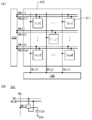
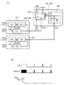
도 1은 메모리의 구성예를 도시한 블록도.
도 2의 (A)는 메모리 셀 어레이를 설명하는 도면이고, 도 2의 (B)는 메모리 셀의 구성예를 도시한 회로도.
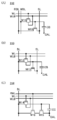
도 3의 (A), (B), (C)는 메모리 셀의 구성예를 도시한 회로도.
도 4의 (A)는 워드선 드라이버 회로의 구성예를 도시한 블록도이고, 도 4의 (B)는 회로(LVB)의 구성예를 도시한 회로도.
도 5의 (A), (B)는 워드선 드라이버 회로의 입출력의 예를 도시한 도면.
도 6의 (A), (B)는 전위 생성 회로의 구성예를 도시한 회로도.
도 7은 메모리 셀 어레이와 비트선 드라이버 회로의 구성예를 설명하는 도면.
도 8은 회로 구성예를 설명하는 도면.
도 9는 기억 장치의 동작예를 설명하는 타이밍 차트.
도 10은 기억 장치의 동작예를 설명하는 타이밍 차트.
도 11은 기억 장치의 동작예를 설명하는 타이밍 차트.
도 12는 반도체 장치의 구성예를 도시한 단면도.
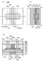
도 13의 (A), (B), (C)는 트랜지스터의 구조예를 도시한 단면도.
도 14의 (A)는 트랜지스터의 구조예를 도시한 상면도이고, 도 14의 (B), (C)는 트랜지스터의 구조예를 도시한 단면도.
도 15의 (A)는 트랜지스터의 구조예를 도시한 상면도이고, 도 15의 (B), (C)는 트랜지스터의 구조예를 도시한 단면도.
도 16의 (A)는 트랜지스터의 구조예를 도시한 상면도이고, 도 16의 (B), (C)는 트랜지스터의 구조예를 도시한 단면도.
도 17의 (A)는 트랜지스터의 구조예를 도시한 상면도이고, 도 17의 (B), (C)는 트랜지스터의 구조예를 도시한 단면도.
도 18의 (A)는 트랜지스터의 구조예를 도시한 상면도이고, 도 18의 (B), (C)는 트랜지스터의 구조예를 도시한 단면도.
도 19의 (A)는 트랜지스터의 구조예를 도시한 상면도이고, 도 19의 (B)는 트랜지스터의 구조예를 도시한 사시도.
도 20의 (A), (B)는 트랜지스터의 구조예를 도시한 단면도.
도 21의 (A), (C)는 트랜지스터의 단면도이고, 도 21의 (B), (D)는 트랜지스터의 전기 특성을 도시한 도면.
도 22는 제품 이미지를 설명하는 도면.
도 23의 (A), (B), (C), (D), (E1), (E2)는 전자 기기의 구성예를 도시한 도면.
도 24는 트랜지스터의 VG-ID 특성의 온도 의존성을 설명하는 도면.
도 25의 (A), (B), (C)는 동작 주파수의 산출 방법을 설명하는 도면.
도 26은 동작 주파수의 산출 결과를 도시한 도면.
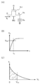
도 27의 (A)는 트랜지스터 구조를 도시한 사시도이고, 도 27의 (B)는 Id-Vg 특성의 백 게이트 전압 의존성을 도시한 도면.
도 28의 (A)는 전계 효과 이동도(μFE)의 백 게이트 전압(Vbg) 의존성을 도시한 도면이고, 도 28의 (B)는 문턱 전압(Vth)의 백 게이트 전압(Vbg) 의존성을 도시한 도면.
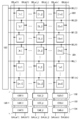
도 29는 64kb DOSRAM의 블록도.
도 30의 (A)는 CAAC-IGZO FET의 Id-Vg 특성을 도시한 도면이고, 도 30의 (B), (C)는 동작 전압을 도시한 도면.
도 31은 DOSRAM의 데이터 유지 상황의 평가 결과를 도시한 도면.
도 32의 (A), (B)는 85℃의 환경 온도하에서의 유지 시간과 수율의 평가 결과.
도 33의 (A)는 음 전위 생성 회로의 블록도이고, 도 33의 (B)는 음 전위 생성 회로의 동작 파형을 도시한 도면.
도 34의 (A)는 링 오실레이터의 동작 조건을 도시한 도면이고, 도 34의 (B)는 차지 펌프의 동작 조건을 도시한 도면.
도 35의 (A)는 콤퍼레이터의 회로도이고, 도 35의 (B)는 콤퍼레이터의 동작 파형을 도시한 도면.
도 36은 1Mb DOSRAM의 소비전력과 점유 면적의 추산 결과.
도 37은 시작(試作)한 DOSRAM의 칩 사진.1 is a block diagram showing a configuration example of a memory.
Fig. 2A is a diagram illustrating a memory cell array, and Fig. 2B is a circuit diagram showing a configuration example of a memory cell.
3A, 3B, and 3C are circuit diagrams showing a configuration example of a memory cell.
Fig. 4A is a block diagram showing a configuration example of a word line driver circuit, and Fig. 4B is a circuit diagram showing a configuration example of a circuit LVB.
5A and 5B are diagrams showing examples of input/output of a word line driver circuit.
6A and 6B are circuit diagrams showing a configuration example of a potential generation circuit.
Fig. 7 is a diagram for explaining a configuration example of a memory cell array and a bit line driver circuit.
8 is a diagram for explaining an example of a circuit configuration.
9 is a timing chart for explaining an operation example of a storage device.
10 is a timing chart for explaining an operation example of a storage device.
11 is a timing chart for explaining an operation example of a storage device.
12 is a cross-sectional view showing a configuration example of a semiconductor device.
13A, 13B, and 13C are cross-sectional views illustrating a structural example of a transistor.
14A is a top view showing a structure example of a transistor, and FIGS. 14B and 14C are sectional views showing a structure example of a transistor.
Fig. 15A is a top view showing a structure example of a transistor, and Figs. 15B and 15C are sectional views showing a structure example of a transistor.
Fig. 16A is a top view showing a structure example of a transistor, and Figs. 16B and 16C are sectional views showing a structure example of a transistor.
Fig. 17A is a top view showing a structure example of a transistor, and Figs. 17B and 17C are sectional views showing a structure example of a transistor.
Fig. 18A is a top view showing a structure example of a transistor, and Figs. 18B and 18C are sectional views showing a structure example of a transistor.
Fig. 19(A) is a top view showing a structure example of a transistor, and Fig. 19(B) is a perspective view showing a structure example of a transistor.
20A and 20B are cross-sectional views showing a structural example of a transistor.
21A and 21C are cross-sectional views of a transistor, and FIGS. 21B and 21D are views showing electrical characteristics of the transistor.
22 is a diagram for explaining a product image.
23(A), (B), (C), (D), (E1), and (E2) are diagrams showing configuration examples of electronic devices.
Fig. 24 is a diagram for explaining the temperature dependence of V G -I D characteristics of a transistor.
25(A), (B), and (C) are diagrams for explaining a method of calculating an operating frequency.
26 is a diagram showing a calculation result of an operating frequency.
Fig. 27(A) is a perspective view showing a transistor structure, and Fig. 27(B) is a view showing the back gate voltage dependence of the Id-Vg characteristic.
(A) of FIG. 28 is a diagram showing the dependence of the field effect mobility (μFE) on the back gate voltage (Vbg), and (B) of FIG. 28 shows the dependence of the threshold voltage (Vth) on the back gate voltage (Vbg) One drawing.
Fig. 29 is a block diagram of a 64kb DOSRAM.
FIG. 30A is a diagram showing Id-Vg characteristics of a CAAC-IGZO FET, and FIGS. 30B and 30C are diagrams showing operating voltages.
Fig. 31 is a diagram showing an evaluation result of the data retention status of the DOSRAM.
32(A) and (B) are evaluation results of holding time and yield under an environmental temperature of 85°C.
Fig. 33A is a block diagram of a negative potential generation circuit, and Fig. 33B is a diagram showing an operation waveform of the negative potential generation circuit.
Fig. 34A is a diagram showing the operating conditions of the ring oscillator, and Fig. 34B is a diagram showing the operating conditions of the charge pump.
Fig. 35(A) is a circuit diagram of a comparator, and Fig. 35(B) is a diagram showing an operation waveform of the comparator.
36 is an estimation result of power consumption and occupied area of 1Mb DOSRAM.
Fig. 37 is a photograph of a chip of a DOSRAM started.
이하에서, 실시형태에 대하여 도면을 참조하면서 설명한다. 다만, 실시형태는 많은 상이한 형태로 실시될 수 있으며, 취지 및 그 범위에서 벗어남이 없이 그 형태 및 자세한 사항을 다양하게 변경할 수 있는 것은 통상의 기술자라면 용이하게 이해할 수 있다. 따라서, 본 발명은 이하의 실시형태의 기재 내용에 한정하여 해석되는 것은 아니다.Hereinafter, embodiments will be described with reference to the drawings. However, the embodiments may be implemented in many different forms, and it may be easily understood by those of ordinary skill in the art that the form and details may be variously changed without departing from the spirit and scope. Therefore, the present invention is not interpreted as being limited to the description of the following embodiments.
또한, 이하에 나타내는 복수의 실시형태는 적절히 조합할 수 있다. 또한, 하나의 실시형태 중에서 복수의 구성예가 나타내어지는 경우에는, 구성예를 서로 적절히 조합할 수 있다.In addition, a plurality of embodiments shown below can be appropriately combined. In addition, when a plurality of configuration examples are shown in one embodiment, configuration examples can be appropriately combined with each other.
또한, 본 명세서에 첨부된 도면에서는 구성 요소를 기능마다 분류하여 서로 독립된 블록으로서 블록도를 도시하였지만, 실제의 구성 요소들을 기능마다 완전히 나누는 것이 어려우며 하나의 구성 요소가 복수의 기능에 관련될 수도 있다.In addition, in the drawings attached to the present specification, components are classified for each function and a block diagram is shown as independent blocks, but it is difficult to completely divide the actual components for each function, and one component may be related to a plurality of functions. .
또한, 도면 등에서 크기, 층의 두께, 영역 등은 명료화를 위하여 과장되어 있는 경우가 있다. 따라서, 반드시 그 스케일에 한정되는 것은 아니다. 도면은 이상적인 예를 모식적으로 도시한 것이고, 도면에 도시한 형상 또는 값 등에 한정되지 않는다.In addition, in the drawings, the size, layer thickness, and area are sometimes exaggerated for clarity. Therefore, it is not necessarily limited to that scale. The drawings schematically show an ideal example, and are not limited to the shapes or values shown in the drawings.
또한, 도면 등에서 동일한 요소들 또는 비슷한 기능을 가지는 요소들, 동일한 재질의 요소들, 또는 동시에 형성되는 요소들 등에는 동일한 부호를 부여하는 경우가 있고, 그 반복 설명을 생략하는 경우가 있다.In addition, in the drawings, the same elements or elements having a similar function, elements of the same material, or elements formed at the same time may be given the same reference numerals, and repeated descriptions thereof may be omitted.
또한, 본 명세서 등에서, "막"이라는 용어와 "층"이라는 용어는 서로 바꿀 수 있다. 예를 들어, "도전층"이라는 용어를 "도전막"이라는 용어로 변경할 수 있는 경우가 있다. 또는, 예를 들어 "절연막"이라는 용어를 "절연층"이라는 용어로 바꿀 수 있는 경우가 있다.In addition, in this specification and the like, the terms "film" and "layer" may be interchanged. For example, in some cases, the term "conductive layer" can be changed to the term "conductive film". Or, for example, there is a case where the term "insulation film" can be replaced with the term "insulation layer".
또한, 본 명세서 등에서 "위"나 "아래" 등 배치를 나타내는 용어는 구성 요소의 위치 관계가 "바로 위" 또는 "바로 아래"인 것을 한정하는 것이 아니다. 예를 들어 "게이트 절연층 위의 게이트 전극"이라는 표현이라면 게이트 절연층과 게이트 전극 사이에 다른 구성 요소를 포함하는 것을 제외하지 않는다.In addition, terms indicating an arrangement such as "above" or "bottom" in the present specification and the like do not limit that the positional relationship of a component is "right above" or "right below". For example, the expression "a gate electrode on a gate insulating layer" does not exclude the inclusion of other components between the gate insulating layer and the gate electrode.
또한, 본 명세서 등에서 "제 1", "제 2", "제 3" 등의 서수사는 구성 요소의 혼동을 피하기 위하여 붙인 것이고, 수적으로 한정하는 것이 아니다.In addition, in this specification and the like, ordinal numbers such as "first", "second", and "third" are attached to avoid confusion of constituent elements, and are not limited in number.
또한, 본 명세서 등에서, "전기적으로 접속"이란, "어떠한 전기적 작용을 가지는 것"을 통하여 접속되어 있는 경우가 포함된다. 여기서, "어떠한 전기적 작용을 가지는 것"은 접속 대상 간에서의 전기 신호의 주고받음을 가능하게 하는 것이면 특별한 제한을 받지 않는다. 예를 들어, "어떠한 전기적 작용을 가지는 것"에는 전극이나 배선을 비롯하여 트랜지스터 등의 스위칭 소자, 저항 소자, 인덕터, 용량 소자, 이 외 각종 기능을 가지는 소자 등이 포함된다.In addition, in this specification and the like, the term "electrically connected" includes the case of being connected through "having some electrical action". Here, "having some electrical action" is not subject to any particular limitation as long as it enables the exchange of electrical signals between the objects to be connected. For example, "having an electrical action" includes electrodes or wirings, switching elements such as transistors, resistance elements, inductors, capacitors, and elements having various functions.
또한, 본 명세서 등에서 "전압"이란 어떤 전위와 기준 전위(예를 들어, 그라운드 전위)의 전위차를 가리키는 경우가 많다. 따라서, 전압과 전위차는 바꿔 말할 수 있다.In addition, in this specification and the like, "voltage" often refers to a potential difference between a certain potential and a reference potential (for example, a ground potential). Thus, the voltage and potential difference can be in turn.
또한, 본 명세서 등에서 트랜지스터란 게이트와 드레인과 소스를 포함하는 적어도 3개의 단자를 가지는 소자이다. 그리고, 드레인(드레인 단자, 드레인 영역, 또는 드레인 전극)과 소스(소스 단자, 소스 영역, 또는 소스 전극) 사이에 채널 형성 영역을 가지고, 채널 형성 영역을 통하여 소스와 드레인 사이에 전류를 흘릴 수 있는 것이다. 또한, 본 명세서 등에서 채널 형성 영역이란, 전류가 주로 흐르는 영역을 말한다.In addition, in this specification and the like, a transistor is a device having at least three terminals including a gate, a drain, and a source. In addition, it has a channel formation region between the drain (drain terminal, drain region, or drain electrode) and the source (source terminal, source region, or source electrode), and a current can flow between the source and the drain through the channel formation region. will be. In addition, in this specification and the like, the channel formation region refers to a region through which current mainly flows.
또한, 소스나 드레인의 기능은 상이한 극성의 트랜지스터를 채용하는 경우나, 회로 동작에서 전류의 방향이 변화되는 경우 등에는 바뀌는 경우가 있다. 그래서, 본 명세서 등에서 소스나 드레인이라는 용어는 서로 바꿔 사용할 수 있는 것으로 한다.In addition, the function of the source and the drain may change when transistors of different polarities are employed, when the direction of current changes in circuit operation, and the like. Therefore, in this specification and the like, the terms source and drain are assumed to be interchangeable.
또한, 본 명세서 등에서 특별히 언급하지 않는 경우, 오프 전류란 트랜지스터가 오프 상태(비도통 상태, 차단 상태라고도 함)일 때의 드레인 전류를 말한다. 오프 상태란, 특별히 언급하지 않는 경우, n채널형 트랜지스터에서는 소스에 대한 게이트의 전압(Vgs)이 문턱 전압(Vth)보다 낮은 상태, p채널형 트랜지스터에서는 소스에 대한 게이트의 전압(Vgs)이 문턱 전압(Vth)보다 높은 상태를 말한다. 즉, n채널형 트랜지스터의 오프 전류란, 소스에 대한 게이트의 전압(Vgs)이 문턱 전압(Vth)보다 낮을 때의 드레인 전류를 말하는 경우가 있다.In addition, unless specifically stated in this specification or the like, the off current refers to a drain current when the transistor is in an off state (also referred to as a non-conducting state or a cut-off state). The off state is a state in which the voltage (Vgs) of the gate to the source is lower than the threshold voltage (Vth) in the n-channel transistor, and the voltage (Vgs) of the gate to the source is lower in the p-channel transistor. It refers to a state higher than the voltage (Vth). That is, the off current of the n-channel transistor may refer to the drain current when the voltage Vgs of the gate to the source is lower than the threshold voltage Vth.
상기 오프 전류의 설명에서 드레인을 소스로 바꿔 읽어도 좋다. 즉, 오프 전류란, 트랜지스터가 오프 상태일 때의 소스 전류를 말하는 경우가 있다. 또한, 오프 전류와 같은 의미로 누설 전류라고 하는 경우가 있다. 또한, 본 명세서 등에서 오프 전류란 트랜지스터가 오프 상태일 때에 소스와 드레인 사이를 흐르는 전류를 가리키는 경우가 있다.In the description of the off current, the drain may be changed to the source and read. That is, the off current may refer to the source current when the transistor is in the off state. In addition, there is a case of a leakage current in the same sense as the off current. In addition, in this specification and the like, the off current may refer to a current flowing between the source and the drain when the transistor is in the off state.
또한, 본 명세서 등에서, 금속 산화물(metal oxide)이란, 넓은 의미로의 금속의 산화물이다. 금속 산화물은, 산화물 절연체, 산화물 도전체(투명 산화물 도전체를 포함함), 산화물 반도체(Oxide Semiconductor라고도 함) 등으로 분류된다.In addition, in this specification and the like, a metal oxide is an oxide of a metal in a broad sense. Metal oxides are classified into oxide insulators, oxide conductors (including transparent oxide conductors), oxide semiconductors (also referred to as oxide semiconductors), and the like.
예를 들어, 트랜지스터의 채널 형성 영역에 금속 산화물을 사용한 경우, 상기 금속 산화물을 산화물 반도체라고 부르는 경우가 있다. 즉 금속 산화물이 증폭 작용, 정류 작용, 및 스위칭 작용 중 적어도 하나를 가지는 경우, 상기 금속 산화물을 금속 산화물 반도체(metal oxide semiconductor)라고 부를 수 있다. 즉 채널 형성 영역에 금속 산화물을 가지는 트랜지스터를 "산화물 반도체 트랜지스터", "OS 트랜지스터"라고 부를 수 있다. 마찬가지로, 상술한 "산화물 반도체를 사용한 트랜지스터"도 채널 형성 영역에 금속 산화물을 가지는 트랜지스터이다.For example, when a metal oxide is used in the channel formation region of a transistor, the metal oxide is sometimes referred to as an oxide semiconductor. That is, when the metal oxide has at least one of an amplification action, a rectification action, and a switching action, the metal oxide may be referred to as a metal oxide semiconductor. That is, a transistor having a metal oxide in the channel formation region may be referred to as an "oxide semiconductor transistor" or an "OS transistor". Similarly, the "transistor using an oxide semiconductor" described above is also a transistor having a metal oxide in the channel formation region.
또한, 본 명세서 등에서 질소를 가지는 금속 산화물도 금속 산화물(metal oxide)이라고 부르는 경우가 있다. 또한, 질소를 가지는 금속 산화물을 금속 산질화물(metal oxynitride)이라고 불러도 좋다. 금속 산화물의 자세한 사항에 대해서는 후술한다.In addition, in the present specification and the like, a metal oxide having nitrogen is sometimes referred to as a metal oxide. Further, a metal oxide containing nitrogen may be referred to as a metal oxynitride. Details of the metal oxide will be described later.
(실시형태 1)(Embodiment 1)
본 실시형태에서는 본 발명의 일 형태에 따른 기억 장치의 구성예에 대하여 설명한다. 본 발명의 일 형태에 따른 기억 장치는 반도체 특성을 이용함으로써 기능할 수 있는 기억 장치이고, 메모리라고도 불린다.In this embodiment, a configuration example of a storage device according to one embodiment of the present invention will be described. A memory device according to an embodiment of the present invention is a memory device that can function by utilizing semiconductor characteristics, and is also called a memory.
<메모리의 구성예><Memory configuration example>
도 1은 본 발명의 일 형태에 따른 메모리(100)의 구성예를 도시한 블록도이다. 메모리(100)는 주변 회로(111) 및 메모리 셀 어레이(201)(도 1에는 "Memory Cell Array"라고 표기하였음)를 가진다. 주변 회로(111)는 행 디코더(121), 워드선 드라이버 회로(122), 비트선 드라이버 회로(130), 출력 회로(140), 음 전위 생성 회로(150), 음 전위 생성 회로(151), 컨트롤 로직 회로(160)를 가진다. 또한, 본 명세서 등에서 설명하는 도면에 있어서, 주된 신호의 흐름을 화살표 또는 선으로 나타내고, 전원선 등은 생략하는 경우가 있다.1 is a block diagram showing a configuration example of a
비트선 드라이버 회로(130)는 열 디코더(column decoder)(131), 프리차지 회로(132), 감지 증폭기(133), 및 입출력 회로(134)를 가진다. 프리차지 회로(132)는 배선(BL)을 프리차지하는 기능을 가진다. 감지 증폭기(133)는 배선(BL)으로부터 판독된 데이터 신호를 증폭하는 기능을 가지고, 입출력 회로(134)는 배선(BL)에 데이터 신호를 기록하는 기능 및 배선(BL)으로부터 판독한 데이터 신호를 출력 회로(140)로 출력하는 기능을 가진다. 또한, 열 디코더(131), 프리차지 회로(132), 감지 증폭기(133) 등의 자세한 사항에 대해서는, 실시형태 2에서 설명한다.The bit
배선(BL), 배선(WL), 및 배선(WLB)은 메모리 셀 어레이(201)가 가지는 메모리 셀(211)(도 1에는 "Memory Cell"이라고 표기하였음)에 접속되어 있는 배선이고, 자세한 사항은 후술한다. 증폭된 데이터 신호는 출력 회로(140)를 통하여 디지털의 데이터 신호(RDATA)로서 메모리(100)의 외부로 출력된다.The wiring BL, the wiring WL, and the wiring WLB are wirings connected to the memory cell 211 (indicated as “Memory Cell” in FIG. 1) of the
메모리(100)에는 외부로부터 전원으로서 저전원 전위(VSS), 주변 회로(111)용 고전원 전위(VDD), 메모리 셀 어레이(201)용 고전원 전위(VIH)가 공급된다. 여기서, 고전원 전위(VDD)는 저전원 전위(VSS)보다 높은 전위이다. 또한, 예를 들어 고전원 전위(VIH)는 고전원 전위(VDD)보다 높은 전위, 또는 고전원 전위(VDD)와 같은 전위로 할 수 있다.A low power source potential (VSS), a high power source potential (VDD) for the
또한, 외부로부터 공급된 전원으로부터, 음 전위 생성 회로(150)는 저전원 전위(VLL)를 생성하고, 음 전위 생성 회로(151)는 저전원 전위(VBL)를 생성한다. 저전원 전위(VLL) 및 저전원 전위(VBL)는 저전원 전위(VSS)보다 낮은 전위이다. 또한, 메모리(100)를 음 전위 생성 회로(150) 및 음 전위 생성 회로(151)를 가지지 않는 구성으로 하고, 저전원 전위(VLL) 및 저전원 전위(VBL)를 메모리(100)의 외부로부터 공급하여도 좋다.Further, from a power supplied from the outside, the negative
메모리(100)에는 제어 신호(CE, WE, RE), 어드레스 신호(ADDR), 데이터 신호(WDATA)가 외부로부터 입력된다. 어드레스 신호(ADDR)는 행 디코더(121) 및 열 디코더(131)에 입력되고, WDATA는 입출력 회로(134)에 입력된다.Control signals CE, WE, and RE, address signals ADDR, and data signals WDATA are externally input to the
컨트롤 로직 회로(160)는 외부로부터의 입력 신호(CE, WE, RE)를 처리하여 행 디코더(121), 열 디코더(131)의 제어 신호를 생성한다. CE는 칩 인에이블 신호이고, WE는 기록 인에이블 신호이고, RE는 판독 인에이블 신호이다. 컨트롤 로직 회로(160)가 처리하는 신호는 이에 한정되는 것이 아니고, 필요에 따라 다른 제어 신호를 입력하여도 좋다.The
또한, 메모리(100)에서 상술한 각 회로, 각 신호, 및 각 전위는 필요에 따라 적절히 취사할 수 있다. 또는 다른 회로, 다른 신호, 또는 다른 전위를 추가하여도 좋다.In addition, each circuit, each signal, and each potential described above in the
여기서, 메모리 셀(211)을 구성하는 트랜지스터에 OS 트랜지스터를 적용할 수 있다. OS 트랜지스터는 오프 전류가 매우 작기 때문에, 메모리 셀(211)에 기록된 데이터를 장시간 유지할 수 있다. 그러므로, 메모리 셀(211)의 리프레시 빈도를 낮게 할 수 있고, 메모리(100)를 소비전력이 적은 메모리로 할 수 있다. 또한, OS 트랜지스터의 자세한 사항에 대해서는, 실시형태 3 및 실시형태 4에서 설명한다.Here, an OS transistor may be applied to a transistor constituting the
또한, OS 트랜지스터는 박막 트랜지스터이고, 반도체 기판 위에 적층하여 제공할 수 있다. 예를 들어, 주변 회로(111)를 구성하는 트랜지스터에 단결정 실리콘 기판에 형성된 Si 트랜지스터를 적용할 수 있다. Si 트랜지스터를 적용한 주변 회로(111)는 고속 동작이 가능하다. 그리고, OS 트랜지스터를 적용한 메모리 셀(211)은 주변 회로(111)의 위쪽에 적층하여 제공할 수 있다.Further, the OS transistor is a thin film transistor, and can be provided by stacking on a semiconductor substrate. For example, a Si transistor formed on a single crystal silicon substrate can be applied to a transistor constituting the
도 2의 (A)에 메모리 셀 어레이(201)의 자세한 사항을 기재한다. 메모리 셀 어레이(201)는 1열에 m(m은 1 이상의 정수)개, 1행에 n(n은 1 이상의 정수)개, 총 m×n개의 메모리 셀(211)을 가지고, 메모리 셀(211)은 매트릭스상으로 배치되어 있다. 도 2의 (A)에서는 메모리 셀(211)의 어드레스도 표기하였고, [1, 1], [m, 1], [i, j], [1, n], [m, n](i는 1 이상 m 이하의 정수이고, j는 1 이상 n 이하의 정수임)은 메모리 셀(211)의 어드레스이다.Details of the
또한, 각 메모리 셀(211)은 배선(BL), 배선(WL), 및 배선(WLB)과 접속되어 있다. 메모리 셀 어레이(201)는 n개의 배선(BL)(BL(1) 내지 BL(n))과 m개의 배선(WL)(WL(1) 내지 WL(m)), 및 m개의 배선(WLB)(WLB(1) 내지 WLB(m))을 가진다. 도 2의 (A)에 도시한 바와 같이, 어드레스가 [i, j]의 메모리 셀(211)은 배선(WL(i)) 및 배선(WLB(i))을 통하여 워드선 드라이버 회로(122)와 전기적으로 접속되고, 배선(BL(j))을 통하여 비트선 드라이버 회로(130)와 전기적으로 접속된다.In addition, each
<메모리 셀의 구성예><Configuration example of memory cell>
도 2의 (B)는 메모리 셀(211)의 구성예를 도시한 회로도이다.2B is a circuit diagram showing a configuration example of the
메모리 셀(211)은 트랜지스터(M11)와 용량 소자(CA)를 가진다. 또한, 트랜지스터(M11)는 프런트 게이트(단순히 게이트라고 부르는 경우가 있음) 및 백 게이트를 가진다.The
트랜지스터(M11)의 소스 및 드레인 중 한쪽은 용량 소자(CA)의 제 1 단자와 전기적으로 접속되고, 트랜지스터(M11)의 소스 및 드레인 중 다른 쪽은 배선(BL)과 접속된다. 트랜지스터(M11)의 게이트는 배선(WL)과 접속되고, 트랜지스터(M11)의 백 게이트는 배선(WLB)과 접속된다. 용량 소자(CA)의 제 2 단자는 배선(CAL)과 접속된다.One of the source and drain of the transistor M11 is electrically connected to the first terminal of the capacitor element CA, and the other of the source and drain of the transistor M11 is connected to the wiring BL. The gate of the transistor M11 is connected to the wiring WL, and the back gate of the transistor M11 is connected to the wiring WLB. The second terminal of the capacitive element CA is connected to the wiring CAL.
배선(BL)은 비트선으로서 기능하고, 배선(WL)은 워드선으로서 기능한다. 배선(CAL)은 용량 소자(CA)의 제 2 단자에 소정의 전위를 인가하기 위한 배선으로서 기능한다. 또한, 배선(WLB)은 트랜지스터(M11)의 백 게이트에 전위를 인가하기 위한 배선으로서 기능한다. 배선(WLB)에 임의의 전위를 인가함으로써, 트랜지스터(M11)의 문턱 전압을 증감시킬 수 있다.The wiring BL functions as a bit line, and the wiring WL functions as a word line. The wiring CAL functions as a wiring for applying a predetermined potential to the second terminal of the capacitor element CA. Further, the wiring WLB functions as a wiring for applying a potential to the back gate of the transistor M11. By applying an arbitrary potential to the wiring WLB, the threshold voltage of the transistor M11 can be increased or decreased.
트랜지스터(M11)는 용량 소자(CA)의 제 1 단자와 배선(BL)을 도통 또는 비도통으로 하는 스위치로서의 기능을 가진다. 데이터의 기록 또는 판독은 배선(WL)에 하이 레벨의 전위를 인가하고 용량 소자(CA)의 제 1 단자와 배선(BL)을 도통 상태로 함으로써 수행된다. 즉, 메모리 셀(211)은 용량 소자(CA)에 전하를 축적함으로써 데이터를 유지하는 메모리이고, 메모리 셀(211)에 유지되는 데이터는 배선(BL) 및 트랜지스터(M11)를 통하여 기록 또는 판독된다.The transistor M11 has a function as a switch that makes the first terminal of the capacitor element CA and the wiring BL conduct or not. Data writing or reading is performed by applying a high-level potential to the wiring WL and making the first terminal of the capacitor element CA and the wiring BL conductive. That is, the
또한, 트랜지스터(M11)에는 채널 형성 영역에 금속 산화물을 가지는 트랜지스터(OS 트랜지스터)를 사용할 수 있다. 예를 들어, 트랜지스터(M11)의 채널 형성 영역에 인듐, 원소 M(원소 M은 알루미늄, 갈륨, 이트륨, 구리, 바나듐, 베릴륨, 붕소, 타이타늄, 철, 니켈, 저마늄, 지르코늄, 몰리브데넘, 란타넘, 세륨, 네오디뮴, 하프늄, 탄탈럼, 텅스텐, 및 마그네슘 등에서 선택된 1종류 또는 복수 종류), 아연 중 어느 하나를 가지는 금속 산화물을 사용할 수 있다. 특히, 인듐, 갈륨, 아연으로 이루어지는 금속 산화물인 것이 바람직하다.In addition, a transistor (OS transistor) having a metal oxide in the channel formation region may be used for the transistor M11. For example, indium, element M in the channel formation region of the transistor M11 (element M is aluminum, gallium, yttrium, copper, vanadium, beryllium, boron, titanium, iron, nickel, germanium, zirconium, molybdenum, One or more types selected from lanthanum, cerium, neodymium, hafnium, tantalum, tungsten, and magnesium) and zinc may be used. In particular, it is preferably a metal oxide composed of indium, gallium, and zinc.
OS 트랜지스터는 오프 전류가 매우 작기 때문에, 트랜지스터(M11)에 OS 트랜지스터를 사용함으로써 메모리 셀(211)에 기록한 데이터를 장시간에 걸쳐 유지할 수 있다. 그러므로, 메모리 셀(211)의 리프레시 빈도를 낮게 할 수 있고, 메모리(100)를 소비전력이 적은 메모리로 할 수 있다.Since the OS transistor has a very small off current, data written to the
또는, 트랜지스터(M11)에 OS 트랜지스터를 사용함으로써, 메모리 셀(211)의 리프레시 동작을 불필요하게 할 수 있다. 또는, 트랜지스터(M11)에 OS 트랜지스터를 사용함으로써, 메모리 셀(211)에 멀티레벨 데이터 또는 아날로그 데이터를 유지할 수 있다.Alternatively, by using the OS transistor for the transistor M11, the refresh operation of the
트랜지스터(M11)에 OS 트랜지스터를 사용함으로써, 상술한 DOSRAM을 구성할 수 있다.By using the OS transistor for the transistor M11, the DOSRAM described above can be configured.
<메모리 셀의 구성예 2><Configuration example 2 of memory cell>
또한, 메모리 셀(211)은 상기 구성에 한정되는 것이 아니다. 도 3의 (A)에 도시된 메모리 셀(212)은 메모리 셀(211)의 다른 구성예이다.In addition, the
메모리 셀(212)은 트랜지스터(M12)와 트랜지스터(M13)와 용량 소자(CB)를 가진다. 트랜지스터(M12)는 프런트 게이트 및 백 게이트를 가진다.The
트랜지스터(M12)의 소스 및 드레인 중 한쪽은 용량 소자(CB)의 제 1 단자 및 트랜지스터(M13)의 게이트와 전기적으로 접속되고, 트랜지스터(M12)의 소스 및 드레인 중 다른 쪽은 배선(WBL)과 접속된다. 트랜지스터(M12)의 게이트는 배선(WL)과 접속되고, 트랜지스터(M12)의 백 게이트는 배선(WLB)과 접속된다. 용량 소자(CB)의 제 2 단자는 배선(CAL)과 접속된다. 트랜지스터(M13)의 소스 및 드레인 중 한쪽은 배선(SL)과 접속되고, 트랜지스터(M13)의 소스 및 드레인 중 다른 쪽은 배선(RBL)과 접속된다.One of the source and drain of the transistor M12 is electrically connected to the first terminal of the capacitor element CB and the gate of the transistor M13, and the other of the source and drain of the transistor M12 is connected to the wiring WBL. Connected. The gate of the transistor M12 is connected to the wiring WL, and the back gate of the transistor M12 is connected to the wiring WLB. The second terminal of the capacitor element CB is connected to the wiring CAL. One of the source and drain of the transistor M13 is connected to the wiring SL, and the other of the source and drain of the transistor M13 is connected to the wiring RBL.
배선(WBL)은 기록 비트선으로서 기능하고, 배선(RBL)은 판독 비트선으로서 기능하고, 배선(WL)은 워드선으로서 기능한다. 배선(CAL)은 용량 소자(CB)의 제 2 단자에 소정의 전위를 인가하기 위한 배선으로서 기능한다. 또한, 배선(WLB)은 트랜지스터(M12)의 백 게이트에 전위를 인가하기 위한 배선으로서 기능한다. 배선(WLB)에 임의의 전위를 인가함으로써, 트랜지스터(M12)의 문턱 전압을 증감시킬 수 있다.The wiring WBL functions as a write bit line, the wiring RBL functions as a read bit line, and the wiring WL functions as a word line. The wiring CAL functions as a wiring for applying a predetermined potential to the second terminal of the capacitor element CB. Further, the wiring WLB functions as a wiring for applying a potential to the back gate of the transistor M12. By applying an arbitrary potential to the wiring WLB, the threshold voltage of the transistor M12 can be increased or decreased.
그리고, 트랜지스터(M12)는 용량 소자(CB)의 제 1 단자와 배선(WBL)을 도통 또는 비도통으로 하는 스위치로서의 기능을 가진다.In addition, the transistor M12 has a function as a switch for making the first terminal of the capacitor element CB and the wiring WBL conductive or non-conductive.
데이터의 기록은 배선(WL)에 하이 레벨의 전위를 인가하여 트랜지스터(M12)를 도통 상태로 하고, 용량 소자(CB)의 제 1 단자와 배선(WBL)을 전기적으로 접속함으로써 수행된다. 구체적으로는 트랜지스터(M12)가 도통 상태일 때, 기록하는 데이터에 대응하는 전위를 배선(WBL)에 인가하고, 용량 소자(CB)의 제 1 단자 및 트랜지스터(M13)의 게이트에 상기 전위를 기록한다. 그 후, 배선(WL)에 로 레벨의 전위를 인가하고, 트랜지스터(M12)를 비도통 상태로 함으로써 용량 소자(CB)의 제 1 단자의 전위 및 트랜지스터(M13)의 게이트의 전위를 유지한다.Data writing is performed by applying a high-level potential to the wiring WL to make the transistor M12 conductive, and electrically connecting the first terminal of the capacitor element CB and the wiring WBL. Specifically, when the transistor M12 is in a conductive state, a potential corresponding to the data to be written is applied to the wiring WBL, and the potential is written to the first terminal of the capacitor element CB and the gate of the transistor M13. do. Thereafter, a potential of a low level is applied to the wiring WL, and the potential of the first terminal of the capacitor element CB and the potential of the gate of the transistor M13 are maintained by making the transistor M12 non-conductive.
데이터의 판독은 배선(SL)에 소정의 전위를 인가함으로써 수행된다. 트랜지스터(M13)의 소스와 드레인 사이에 흐르는 전류는 트랜지스터(M13)의 게이트의 전위, 및 트랜지스터(M13)의 소스 및 드레인 중 한쪽(배선(SL))의 전위에 따라 결정되고, 또한 상기 전류에 의하여 트랜지스터(M13)의 소스 및 드레인 중 다른 쪽의 전위가 결정된다. 그러므로, 트랜지스터(M13)의 소스 및 드레인 중 다른 쪽과 접속되는 배선(RBL)의 전위를 판독함으로써 용량 소자(CB)의 제 1 단자(또는 트랜지스터(M13)의 게이트)에 유지되는 전위를 판독할 수 있다. 즉, 용량 소자(CB)의 제 1 단자(또는 트랜지스터(M13)의 게이트)에 유지되어 있는 전위로부터 메모리 셀(212)에 기록되어 있는 데이터를 판독할 수 있다.Data is read by applying a predetermined potential to the wiring SL. The current flowing between the source and drain of the transistor M13 is determined according to the potential of the gate of the transistor M13 and the potential of one of the source and drain of the transistor M13 (wiring SL), and is dependent on the current. Thus, the potential of the other of the source and drain of the transistor M13 is determined. Therefore, by reading the potential of the wiring RBL connected to the other of the source and drain of the transistor M13, the potential held at the first terminal (or the gate of the transistor M13) of the capacitor element CB can be read. I can. That is, data written in the
또한, 트랜지스터(M12)에는 채널 형성 영역에 금속 산화물을 가지는 트랜지스터(OS 트랜지스터)를 사용할 수 있다. OS 트랜지스터는 오프 전류가 매우 작기 때문에, 트랜지스터(M12)로서 OS 트랜지스터를 사용함으로써, 메모리 셀(212)에 기록한 데이터를 장시간에 걸쳐 유지할 수 있다. 또한, 트랜지스터(M13)는 특별히 한정되지 않는다. 예를 들어, 트랜지스터(M13)로서 OS 트랜지스터를 사용하여도 좋고, Si 트랜지스터를 사용하여도 좋다.In addition, a transistor (OS transistor) having a metal oxide in the channel formation region may be used for the transistor M12. Since the OS transistor has a very small off current, data written to the
메모리 셀(212)은 2 트랜지스터 1 용량 소자의 게인 셀형 메모리 셀이다. 게인 셀형 메모리 셀은 용량 소자의 용량이 작은 경우에도 축적된 전하를 가장 가까운 트랜지스터로 증폭함으로써 메모리로서의 동작을 수행할 수 있다. 또한, 트랜지스터(M12)에 오프 전류가 매우 작은 OS 트랜지스터를 사용함으로써 전력의 공급이 정지된 기간에서도 축적된 전하가 유지될 수 있어, 메모리 셀(212)은 비휘발성 메모리로서의 성질을 가진다. OS 트랜지스터를 사용한, 게인 셀형 메모리 셀로 구성되는 메모리를 본 명세서 등에서는 "NOSRAM(Nonvolatile Oxide Semiconductor Random Access Memory)"이라고 부른다. 또한, NOSRAM은 용량 소자의 충방전에 의하여 데이터의 재기록을 수행하기 때문에, 원리적으로는 재기록 횟수에 제한은 없다.The
또한, 메모리 셀(212)은 배선(WBL)과 배선(RBL)을 하나의 배선(BL)으로서 합친 구성이어도 좋다. 배선(WBL)과 배선(RBL)을 하나의 배선(BL)으로서 합친 구성예를 도 3의 (B)에 도시하였다.Further, the
도 3의 (B)에 도시된 메모리 셀(213)에서는 트랜지스터(M12)의 소스 및 드레인 중 다른 쪽 및 트랜지스터(M13)의 소스 및 드레인 중 다른 쪽이 배선(BL)과 접속된다. 즉, 메모리 셀(213)은 기록 비트선과 판독 비트선이 하나의 배선(BL)으로서 동작하는 구성이다. 이 경우, 데이터를 기록할 때는 배선(SL)을 전기적으로 부유 상태(플로팅)로 하는 것이 바람직하다.In the
<메모리 셀의 구성예 3><Configuration example 3 of memory cell>
또한, 메모리 셀(212)을 3 트랜지스터 1 용량 소자의 게인 셀형 메모리 셀로 하여도 좋다. 메모리 셀(212)을 3 트랜지스터 1 용량 소자의 게인 셀형 메모리 셀로 한 경우의 구성예를 도 3의 (C)에 도시하였다.Further, the
도 3의 (C)에 도시된 메모리 셀(214)은 트랜지스터(M14) 내지 트랜지스터(M16)와 용량 소자(CC)를 가진다. 트랜지스터(M14)는 프런트 게이트 및 백 게이트를 가진다.The
트랜지스터(M14)의 소스 및 드레인 중 한쪽은 용량 소자(CC)의 제 1 단자 및 트랜지스터(M15)의 게이트와 전기적으로 접속되고, 트랜지스터(M14)의 소스 및 드레인 중 다른 쪽은 배선(BL)과 접속된다. 트랜지스터(M14)의 게이트는 배선(WL)과 접속되고, 트랜지스터(M14)의 백 게이트는 배선(WLB)과 접속된다. 용량 소자(CC)의 제 2 단자는 배선(CAL) 및 트랜지스터(M15)의 소스 및 드레인 중 한쪽과 전기적으로 접속되고, 트랜지스터(M15)의 소스 및 드레인 중 다른 쪽은 트랜지스터(M16)의 소스 및 드레인 중 한쪽과 전기적으로 접속된다. 트랜지스터(M16)의 소스 및 드레인 중 다른 쪽은 배선(BL)과 접속되고, 트랜지스터(M16)의 게이트는 배선(RWL)과 접속된다.One of the source and drain of the transistor M14 is electrically connected to the first terminal of the capacitor CC and the gate of the transistor M15, and the other of the source and drain of the transistor M14 is connected to the wiring BL. Connected. The gate of the transistor M14 is connected to the wiring WL, and the back gate of the transistor M14 is connected to the wiring WLB. The second terminal of the capacitor CC is electrically connected to one of the wiring CAL and the source and the drain of the transistor M15, and the other of the source and drain of the transistor M15 is the source and the drain of the transistor M16. It is electrically connected to one of the drains. The other of the source and drain of the transistor M16 is connected to the wiring BL, and the gate of the transistor M16 is connected to the wiring RWL.
배선(BL)은 비트선으로서 기능하고, 배선(WL)은 기록 워드선으로서 기능하고, 배선(RWL)은 판독 워드선으로서 기능한다. 배선(CAL)은 용량 소자(CC)의 제 2 단자에 소정의 전위를 인가하기 위한 배선으로서 기능한다(예를 들어 소정의 전위로서 로 레벨의 전위를 인가함). 또한, 배선(WLB)은 트랜지스터(M14)의 백 게이트에 전위를 인가하기 위한 배선으로서 기능한다. 배선(WLB)에 임의의 전위를 인가함으로써, 트랜지스터(M14)의 문턱 전압을 증감시킬 수 있다.The wiring BL functions as a bit line, the wiring WL functions as a write word line, and the wiring RWL functions as a read word line. The wiring CAL functions as a wiring for applying a predetermined potential to the second terminal of the capacitor element CC (for example, applying a low-level potential as a predetermined potential). Further, the wiring WLB functions as a wiring for applying a potential to the back gate of the transistor M14. By applying an arbitrary potential to the wiring WLB, the threshold voltage of the transistor M14 can be increased or decreased.
트랜지스터(M14)는 용량 소자(CC)의 제 1 단자와 배선(BL)을 도통 또는 비도통으로 하는 스위치로서의 기능을 가지고, 트랜지스터(M16)는 트랜지스터(M15)의 소스 및 드레인 중 다른 쪽과 배선(BL)을 도통 또는 비도통으로 하는 스위치로서의 기능을 가진다.Transistor M14 has a function as a switch for conducting or non-conducting the first terminal of the capacitor CC and the wiring BL, and the transistor M16 is connected to the other of the source and drain of the transistor M15 and the wiring ( It has a function as a switch that makes BL) conductive or non-conductive.
데이터의 기록은 배선(WL)에 하이 레벨의 전위를 인가하여 트랜지스터(M14)를 도통 상태로 하고, 용량 소자(CC)의 제 1 단자와 배선(BL)을 전기적으로 접속함으로써 수행된다. 구체적으로는 트랜지스터(M14)가 도통 상태일 때, 기록하는 데이터에 대응하는 전위를 배선(BL)에 인가하고, 용량 소자(CC)의 제 1 단자 및 트랜지스터(M15)의 게이트에 상기 전위를 기록한다. 그 후, 배선(WL)에 로 레벨의 전위를 인가하고, 트랜지스터(M14)를 비도통 상태로 함으로써 용량 소자(CC)의 제 1 단자의 전위 및 트랜지스터(M15)의 게이트의 전위를 유지한다.Data writing is performed by applying a high-level potential to the wiring WL to make the transistor M14 conductive, and electrically connecting the first terminal of the capacitor element CC and the wiring BL. Specifically, when the transistor M14 is in a conductive state, a potential corresponding to the data to be written is applied to the wiring BL, and the potential is written to the first terminal of the capacitor element CC and the gate of the transistor M15. do. Thereafter, a potential of a low level is applied to the wiring WL, and the potential of the first terminal of the capacitor element CC and the potential of the gate of the transistor M15 are maintained by making the transistor M14 non-conductive.
데이터의 판독은 배선(BL)에 소정의 전위를 인가(프리차지)하고, 그 후에 배선(BL)을 전기적으로 부유 상태(플로팅)로 하고, 또한 배선(RWL)에 하이 레벨의 전위를 인가함으로써 수행된다. 배선(RWL)에 하이 레벨의 전위를 인가함으로써 트랜지스터(M16)는 도통 상태가 되고, 트랜지스터(M15)의 소스 및 드레인 중 다른 쪽과 배선(BL)은 전기적으로 접속 상태가 된다. 이때, 트랜지스터(M15)의 소스와 드레인 사이에는 배선(BL)과 배선(CAL)의 전위차에 대응하는 전압이 인가되고, 트랜지스터(M15)의 소스와 드레인 사이를 흐르는 전류는 트랜지스터(M15)의 게이트의 전위 및 상기 소스와 드레인 사이에 인가되는 전압에 따라 결정된다.Data is read by applying (pre-charging) a predetermined potential to the wiring BL, then making the wiring BL electrically floating (floating), and applying a high-level potential to the wiring RWL. Performed. By applying a high-level potential to the wiring RWL, the transistor M16 is in a conductive state, and the other of the source and drain of the transistor M15 and the wiring BL are electrically connected. At this time, a voltage corresponding to the potential difference between the wiring BL and the wiring CAL is applied between the source and the drain of the transistor M15, and the current flowing between the source and the drain of the transistor M15 is the gate of the transistor M15. And the voltage applied between the source and drain.
여기서, 배선(BL)의 전위는 트랜지스터(M15)의 소스와 드레인 사이를 흐르는 전류에 따라 변화하기 때문에, 배선(BL)의 전위를 판독함으로써 용량 소자(CC)의 제 1 단자(또는 트랜지스터(M15)의 게이트)에 유지되어 있는 전위를 판독할 수 있다. 즉, 용량 소자(CC)의 제 1 단자(또는 트랜지스터(M15)의 게이트)에 유지되어 있는 전위로부터 메모리 셀(214)에 기록되어 있는 데이터를 판독할 수 있다.Here, since the potential of the wiring BL changes according to the current flowing between the source and the drain of the transistor M15, the potential of the wiring BL is read to determine the first terminal (or transistor M15) of the capacitor element CC. ), the potential held at the gate) can be read. That is, data written in the
트랜지스터(M14)로서는 채널 형성 영역에 금속 산화물을 가지는 트랜지스터(OS 트랜지스터)를 사용할 수 있다. OS 트랜지스터는 오프 전류가 매우 작기 때문에, 트랜지스터(M14)로서 OS 트랜지스터를 사용함으로써 메모리 셀(214)에 기록한 데이터를 장시간에 걸쳐 유지할 수 있다. 또한, 트랜지스터(M15) 및 트랜지스터(M16)는 특별히 한정되지 않는다. 예를 들어, 트랜지스터(M15) 및 트랜지스터(M16)로서 OS 트랜지스터를 사용하여도 좋고, Si 트랜지스터를 사용하여도 좋다.As the transistor M14, a transistor (OS transistor) having a metal oxide in the channel formation region can be used. Since the OS transistor has a very small off current, data written to the
또한, 도 3의 (A) 내지 (C)를 사용하여 메모리 셀(211)의 다른 구성예를 설명하였지만, 메모리 셀(211)의 구성예는 이들에 한정되지 않고, 회로의 구성을 적절히 변경할 수 있다.In addition, although other configuration examples of the
<워드선 드라이버 회로의 구성예><Configuration example of word line driver circuit>
도 4의 (A)는 워드선 드라이버 회로(122)의 구성예를 도시한 블록도이다.4A is a block diagram showing an example of the configuration of the word
워드선 드라이버 회로(122)는 워드선으로서 기능하는 배선(WL)을 구동하는 기능을 가진다. 워드선 드라이버 회로(122)에는, 배선(WL) 및 배선(WLB)을 구동하기 위한 신호(WI) 및 신호(WIB)가 행 디코더(121)로부터 입력된다. 여기서, 신호(WI) 및 신호(WIB)는 하이 레벨 또는 로 레벨로 나타내어지는 디지털 신호이고, 신호(WIB)는, 신호(WI)의 논리를 반전한 반전 신호이다.The word
또한, 배선(WL) 및 배선(WLB)은 각각 m개 있기 때문에, 신호(WI) 및 신호(WIB)의 개수도 각각 m이다. 도 4의 (A)에서는, WI(1) 내지 WI(m), 및 WIB(1) 내지 WIB(m)라고 나타낸다.Further, since there are m wires WL and WLB, respectively, the number of signals WI and WIB is also m, respectively. In Fig. 4A, they are represented by WI(1) to WI(m) and WIB(1) to WIB(m).
그리고, 행 디코더(121)에는 저전원 전위(VSS)와 고전원 전위(VDD)가 공급되어 있기 때문에, 신호(WI) 및 신호(WIB)의 하이 레벨에 대응하는 전위는 고전원 전위(VDD)이고, 신호(WI) 및 신호(WIB)의 로 레벨에 대응하는 전위는 저전원 전위(VSS)이다.In addition, since the low power supply potential VSS and the high power supply potential VDD are supplied to the
한편, 메모리 셀 어레이(201)에 있어서, 배선(WL)의 하이 레벨에 대응하는 전위로서 고전원 전위(VIH)가 사용되고, 배선(WL)의 로 레벨에 대응하는 전위로서 저전원 전위(VLL)가 사용된다. 또한, 배선(WLB)에는 저전원 전위(VBL)가 공급된다.On the other hand, in the
그러므로, 워드선 드라이버 회로(122)는 입력된 신호의 하이 레벨 또는 로 레벨, 또는 하이 레벨 및 로 레벨을 조정하는(레벨 조정이라고도 함) 기능과, 입력된 신호에 배선(WL)(도 4의 (A)에서는 WL(1) 내지 WL(m)이라고 나타내었음)을 구동하는 능력을 부가하는(버퍼라고도 함) 기능을 가진다. 워드선 드라이버 회로(122)는 회로(LVB)를 m개 가지고, 도 4의 (A)에서는 LVB(1) 내지 LVB(m)로 나타낸다.Therefore, the word
또한, 워드선 드라이버 회로(122)에는 저전원 전위(VBL)가 입력되고, 저전원 전위(VBL)는 배선(WLB)(도 4의 (A)에서는 WLB(1) 내지 WLB(m)로 나타내었음)에 출력된다.In addition, a low power supply potential VBL is input to the word
<회로(LVB)의 구성예><Configuration example of circuit (LVB)>
도 4의 (B)는 회로(LVB)의 구성예를 도시한 회로도이다.4B is a circuit diagram showing a configuration example of a circuit LVB.
회로(LVB)는 n채널형의 트랜지스터(13) 내지 트랜지스터(21), 및 p채널형의 트랜지스터(33) 내지 트랜지스터(41)를 가진다. 또한, 회로(LVB)는 입력 단자(WI_IN), 입력 단자(WIB_IN), 배선(VIH_IN), 배선(VSS_IN), 배선(VLL_IN), 및 출력 단자(WL_OUT)를 가진다.The circuit LVB includes n-
회로(LVB)의 입력 단자(WI_IN)에는 신호(WI)가 입력되고, 입력 단자(WIB_IN)에는 신호(WIB)가 입력되고, 배선(VIH_IN)에는 고전원 전위(VIH)가 입력되고, 배선(VSS_IN)에는 저전원 전위(VSS)가 입력되고, 배선(VLL_IN)에는 저전원 전위(VLL)가 입력된다. 그리고, 회로(LVB)는 출력 단자(WL_OUT)로부터 배선(WL)을 구동하는 신호를 출력한다.The signal WI is input to the input terminal WI_IN of the circuit LVB, the signal WIB is input to the input terminal WIB_IN, the high power potential VIH is input to the wiring VIH_IN, and the wiring ( A low power supply potential VSS is input to VSS_IN), and a low power supply potential VLL is input to wiring VLL_IN. Then, the circuit LVB outputs a signal for driving the wiring WL from the output terminal WL_OUT.
그리고, 회로(LVB)에 있어서, 트랜지스터(13)의 소스 및 드레인 중 한쪽은 배선(VSS_IN)과 전기적으로 접속되고, 트랜지스터(13)의 소스 및 드레인 중 다른 쪽은 트랜지스터(34)의 소스 및 드레인 중 한쪽 및 트랜지스터(35)의 게이트와 전기적으로 접속되고, 트랜지스터(13)의 게이트는 입력 단자(WI_IN) 및 트랜지스터(34)의 게이트와 전기적으로 접속되어 있다. 트랜지스터(34)의 소스 및 드레인 중 다른 쪽은 트랜지스터(33)의 소스 및 드레인 중 한쪽과 전기적으로 접속되고, 트랜지스터(33)의 소스 및 드레인 중 다른 쪽은 배선(VIH_IN)과 전기적으로 접속되어 있다.Further, in the circuit LVB, one of the source and drain of the
트랜지스터(14)의 소스 및 드레인 중 한쪽은 배선(VSS_IN)과 전기적으로 접속되고, 트랜지스터(14)의 소스 및 드레인 중 다른 쪽은 트랜지스터(36)의 소스 및 드레인 중 한쪽 및 트랜지스터(33)의 게이트와 전기적으로 접속되고, 트랜지스터(14)의 게이트는 입력 단자(WIB_IN) 및 트랜지스터(36)의 게이트와 전기적으로 접속되어 있다. 트랜지스터(36)의 소스 및 드레인 중 다른 쪽은 트랜지스터(35)의 소스 및 드레인 중 한쪽과 전기적으로 접속되고, 트랜지스터(35)의 소스 및 드레인 중 다른 쪽은 배선(VIH_IN)과 전기적으로 접속되어 있다. 여기서, 트랜지스터(36)의 소스 및 드레인 중 다른 쪽과 트랜지스터(35)의 소스 및 드레인 중 한쪽의 접속부를 노드(N11)라고 부르고, 노드(N11)와 전기적으로 접속되는 다른 소자 등에 대해서는 후술한다.One of the source and drain of the
트랜지스터(13), 트랜지스터(14), 및 트랜지스터(33) 내지 트랜지스터(36)는 입력된 신호(WI) 및 신호(WIB)의 하이 레벨에 대응하는 전위를 고전원 전위(VDD)로부터 고전원 전위(VIH)로 변환하는 레벨 조정의 기능을 가진다.The
또한, 회로(LVB)에 있어서 트랜지스터(15)의 소스 및 드레인 중 한쪽은 배선(VSS_IN)과 전기적으로 접속되고, 트랜지스터(15)의 소스 및 드레인 중 다른 쪽은 트랜지스터(37)의 소스 및 드레인 중 한쪽, 트랜지스터(16)의 게이트, 및 트랜지스터(38)의 게이트와 전기적으로 접속되고, 트랜지스터(15)의 게이트는 노드(N11) 및 트랜지스터(37)의 게이트와 전기적으로 접속되어 있다. 트랜지스터(37)의 소스 및 드레인 중 다른 쪽은 배선(VIH_IN)과 전기적으로 접속되어 있다. 여기서, 트랜지스터(15)의 소스 및 드레인 중 다른 쪽과 트랜지스터(37)의 소스 및 드레인 중 한쪽, 트랜지스터(16)의 게이트, 및 트랜지스터(38)의 게이트의 접속부를 노드(N12)라고 부르고, 노드(N12)와 전기적으로 접속되는 다른 소자 등에 대해서는 후술한다.In addition, in the circuit LVB, one of the source and drain of the transistor 15 is electrically connected to the wiring VSS_IN, and the other of the source and drain of the transistor 15 is among the source and drain of the
트랜지스터(16)의 소스 및 드레인 중 한쪽은 배선(VSS_IN)과 전기적으로 접속되고, 트랜지스터(16)의 소스 및 드레인 중 다른 쪽은 트랜지스터(38)의 소스 및 드레인 중 한쪽과 전기적으로 접속되고, 트랜지스터(38)의 소스 및 드레인 중 다른 쪽은 배선(VIH_IN)과 전기적으로 접속되어 있다. 여기서, 트랜지스터(16)의 소스 및 드레인 중 다른 쪽과 트랜지스터(38)의 소스 및 드레인 중 한쪽의 접속부를 노드(N13)라고 부르고, 노드(N13)와 전기적으로 접속되는 다른 소자 등에 대해서는 후술한다.One of the source and drain of the
트랜지스터(15) 및 트랜지스터(37)는 노드(N11)의 신호의 반전 신호를 생성하는 기능을 가진다.The transistor 15 and the
또한, 회로(LVB)에 있어서, 트랜지스터(18)의 소스 및 드레인 중 한쪽은 배선(VLL_IN)과 전기적으로 접속되고, 트랜지스터(18)의 소스 및 드레인 중 다른 쪽은 트랜지스터(17)의 소스 및 드레인 중 한쪽과 전기적으로 접속되고, 트랜지스터(17)의 소스 및 드레인 중 다른 쪽은 트랜지스터(39)의 소스 및 드레인 중 한쪽 및 트랜지스터(20)의 게이트와 전기적으로 접속되고, 트랜지스터(39)의 소스 및 드레인 중 다른 쪽은 배선(VIH_IN)과 전기적으로 접속되어 있다. 트랜지스터(17)의 게이트는 노드(N12) 및 트랜지스터(39)의 게이트와 전기적으로 접속되어 있다.Further, in the circuit LVB, one of the source and the drain of the
트랜지스터(20)의 소스 및 드레인 중 한쪽은 배선(VLL_IN)과 전기적으로 접속되고, 트랜지스터(20)의 소스 및 드레인 중 다른 쪽은 트랜지스터(19)의 소스 및 드레인 중 한쪽과 전기적으로 접속되고, 트랜지스터(19)의 소스 및 드레인 중 다른 쪽은 트랜지스터(40)의 소스 및 드레인 중 한쪽 및 트랜지스터(18)의 게이트와 전기적으로 접속되고, 트랜지스터(40)의 소스 및 드레인 중 다른 쪽은 배선(VIH_IN)과 전기적으로 접속되어 있다. 트랜지스터(19)의 게이트는 노드(N13) 및 트랜지스터(40)의 게이트와 전기적으로 접속되어 있다. 여기서, 트랜지스터(20)의 소스 및 드레인 중 다른 쪽과 트랜지스터(19)의 소스 및 드레인 중 한쪽의 접속부를 노드(N14)라고 부르고, 노드(N14)와 전기적으로 접속되는 다른 소자 등에 대해서는 후술한다.One of the source and drain of the
트랜지스터(17) 내지 트랜지스터(20), 트랜지스터(39), 및 트랜지스터(40)는 노드(N12) 및 노드(N13)의 신호의 로 레벨에 대응하는 전위를 저전원 전위(VSS)로부터 저전원 전위(VLL)로 변환하는 레벨 조정 기능을 가진다.The
또한, 회로(LVB)에 있어서, 트랜지스터(21)의 소스 및 드레인 중 한쪽은 배선(VLL_IN)과 전기적으로 접속되고, 트랜지스터(21)의 소스 및 드레인 중 다른 쪽은 트랜지스터(41)의 소스 및 드레인 중 한쪽 및 출력 단자(WL_OUT)와 전기적으로 접속되고, 트랜지스터(21)의 게이트는 노드(N14) 및 트랜지스터(41)의 게이트와 전기적으로 접속되어 있다. 트랜지스터(41)의 소스 및 드레인 중 다른 쪽은 배선(VIH_IN)과 전기적으로 접속되어 있다.Further, in the circuit LVB, one of the source and drain of the
트랜지스터(21) 및 트랜지스터(41)는 노드(N14)의 신호를 출력 단자(WL_OUT)로부터 출력하는 버퍼의 기능을 가진다.The
<워드선 드라이버 회로의 입출력의 예><Example of input/output of word line driver circuit>
도 5의 (A)는 워드선 드라이버 회로(122)의 입출력의 일례를 도시한 도면이다.5A is a diagram showing an example of input/output of the word
도 5의 (A)를 사용하여, 워드선 드라이버 회로(122)에 입력되는 신호(WI) 및 신호(WIB)와, 워드선 드라이버 회로(122)가 구동하는 배선(WL) 및 배선(WLB)의 전위의 관계에 대하여 설명한다. 신호(WI), 신호(WIB), 배선(WL), 및 배선(WLB)은 각각 m개 있기 때문에, 그 중의 하나(WI(i), WIB(i), 배선(WL(i)), 및 WLB(i))를 예로 들어 설명한다(i는 1 이상 m 이하의 정수).Using Fig. 5A, a signal WI and a signal WIB input to the word
도 5의 (A)의 세로축은 전위를 나타내고, 전위는 높은 쪽으로부터 고전원 전위(VIH), 고전원 전위(VDD), 저전원 전위(VSS), 저전원 전위(VLL), 저전원 전위(VBL)인 경우를 도시하였다.The vertical axis of Fig. 5A represents the potential, and the potential is from the higher side to a high power source potential (VIH), a high power source potential (VDD), a low power source potential (VSS), a low power source potential (VLL), and a low power source potential ( VBL) is shown.
도 5의 (A)에서, T1, T2는 시각을 나타내고, 신호(WI(i)) 및 신호(WIB(i))와 거의 같은 시각에 배선(WL(i))이 구동되는 모양을 도시하였다. 또한, 실제로는 입력되는 신호(WI(i)) 및 신호(WIB(i))와 배선(WL(i))이 구동될 때까지에는 지연 시간이 발생하고, 또한 신호에 둔화나 노이즈 등을 가지는 경우가 있다. 도 5의 (A)는 이상적인 경우의 파형을 도시한 것이다.In Fig. 5A, T1 and T2 denote the time, and the wiring WL(i) is driven at approximately the same time as the signal WI(i) and the signal WIB(i). . In addition, a delay time occurs until the input signal (WI(i)), signal (WIB(i)) and wiring (WL(i)) are driven, and the signal has a slowdown or noise. There are cases. Fig. 5A shows waveforms in an ideal case.
도 5의 (A)에 도시한 바와 같이, 신호(WI(i)) 및 신호(WIB(i))는 고전원 전위(VDD) 또는 저전원 전위(VSS)로 하이 레벨 또는 로 레벨을 나타내는 디지털 신호이다. 신호(WI(i))는 배선(WL(i)) 및 배선(WLB(i))과 전기적으로 접속된 메모리 셀(211)에 대하여 데이터의 기록 또는 판독을 수행하는 경우, 하이 레벨이 된다(신호(WIB)는 신호(WI)의 반전 신호이기 때문에 로 레벨이 됨).As shown in (A) of FIG. 5, the signal (WI(i)) and the signal (WIB(i)) represent a high level or a low level with a high power potential (VDD) or a low power potential (VSS). It's a signal. The signal WI(i) becomes a high level when data is written or read for the wiring WL(i) and the
워드선 드라이버 회로(122)는 신호(WI(i))가 로 레벨인 경우, 배선(WL(i))에 저전원 전위(VLL)를 출력하고, 신호(WI(i))가 하이 레벨인 경우, 배선(WL(i))에 고전원 전위(VIH)를 출력한다. 또한, 워드선 드라이버 회로(122)는 배선(WLB(i))에 저전원 전위(VBL)를 출력한다.When the signal WI(i) is at a low level, the word
또는, 워드선 드라이버 회로(122)는 배선(WL)에 더하여 배선(WLB)을 구동하여도 좋다. 워드선 드라이버 회로(122)가 배선(WLB)을 구동하는 경우, 예를 들어 워드선 드라이버 회로(122)에 회로(LVB)를 추가함으로써 수행된다.Alternatively, the word
도 5의 (B)는 도 5의 (A)와 마찬가지로, 워드선 드라이버 회로(122)의 입출력의 일례를 도시한 도면이다. 도 5의 (B)에 도시한 바와 같이, 예를 들어 워드선 드라이버 회로(122)는 신호(WI(i))가 로 레벨인 경우, 배선(WLB(i))에 저전원 전위(VBL)를 출력하고, 신호(WI(i))가 하이 레벨인 경우, 배선(WLB(i))에 고전원 전위(VDD)와 저전원 전위(VSS) 사이의 전위를 출력할 수 있다.5B is a diagram showing an example of input/output of the word
이와 같이, 워드선 드라이버 회로(122)는 신호(WI(i)) 및 신호(WIB(i))의 하이 레벨 또는 로 레벨, 또는 하이 레벨 및 로 레벨을 바꿈으로써 배선(WL(i)) 또는 배선(WL(i)) 및 배선(WLB(i))을 구동한다.In this way, the word
<음 전위 생성 회로><Negative potential generation circuit>
다음으로, 음 전위 생성 회로(150) 및 음 전위 생성 회로(151)에 적용할 수 있는 회로(54) 및 회로(55)의 구성예를 도 6의 (A) 및 (B)에 도시하였다.Next, configuration examples of the
회로(54) 및 회로(55)는 강압형 차지 펌프이고, 입력 단자(IN)에 저전원 전위(VSS)가 입력되고, 출력 단자(OUT)로부터 저전원 전위(VLL) 또는 저전원 전위(VBL)가 출력된다. 여기서는 일례로서 차지 펌프 회로의 기본 회로의 단수는 4단으로 하였지만, 이에 한정되지 않고 임의의 단수로 차지 펌프 회로를 구성하여도 좋다.The
도 6의 (A)에 도시된 회로(54)는 트랜지스터(M21) 내지 트랜지스터(M24) 및 용량 소자(C21) 내지 용량 소자(C24)를 가진다. 또한, 트랜지스터(M21) 내지 트랜지스터(M24)는 n채널형 트랜지스터이다.The
트랜지스터(M21) 내지 트랜지스터(M24)는 입력 단자(IN)와 출력 단자(OUT)사이에 직렬로 접속되어 있다. 트랜지스터(M21) 내지 트랜지스터(M24)에 있어서, 각각의 게이트와 소스 및 드레인 중 한쪽이 전기적으로 접속되고, 트랜지스터(M21) 내지 트랜지스터(M24)는 다이오드로서 기능한다. 또한, 트랜지스터(M21) 내지 트랜지스터(M24)의 게이트에는 각각 용량 소자(C21) 내지 용량 소자(C24)가 전기적으로 접속되어 있다.The transistors M21 to M24 are connected in series between the input terminal IN and the output terminal OUT. In the transistors M21 to M24, each gate and one of the source and drain are electrically connected, and the transistors M21 to M24 function as diodes. Further, the capacitor elements C21 to C24 are electrically connected to the gates of the transistors M21 to M24, respectively.
홀수 단의 용량 소자(C21), 용량 소자(C23)의 한쪽 전극에는 클록 신호(CLK)가 입력되고, 짝수 단의 용량 소자(C22), 용량 소자(C24)의 한쪽 전극에는 클록 신호(CLKB)가 입력된다. 클록 신호(CLKB)는 클록 신호(CLK)의 위상을 반전한 반전 클록 신호이다.A clock signal CLK is input to one electrode of the capacitive element C21 and the capacitive element C23 in the odd-numbered stages, and a clock signal CLKB is applied to one electrode of the capacitive element C22 and the capacitive element C24 in the even-numbered stage. Is entered. The clock signal CLKB is an inverted clock signal obtained by inverting the phase of the clock signal CLK.
회로(54)는 입력 단자(IN)에 입력된 저전원 전위(VSS)를 강압하여 저전원 전위(VLL) 또는 저전원 전위(VBL)를 생성하는 기능을 가진다. 회로(54)는 클록 신호(CLK) 및 클록 신호(CLKB)의 공급만으로 저전원 전위(VSS)를 강압한 저전원 전위(VLL) 또는 저전원 전위(VBL)를 생성할 수 있다.The
도 6의 (B)에 도시된 회로(55)는 p채널형 트랜지스터인 트랜지스터(M31) 내지 트랜지스터(M34)로 구성되어 있다. 그 외의 구성 요소에 대해서는 회로(54)의 설명을 원용한다.The
<트랜지스터(M11)><Transistor (M11)>
상술한 바와 같이, 트랜지스터(M11), 트랜지스터(M12), 및 트랜지스터(M14)로서 백 게이트를 가지는 OS 트랜지스터를 사용할 수 있다. OS 트랜지스터는 백 게이트에 전위를 인가함으로써 문턱 전압을 증감시킬 수 있다. 구체적으로는, OS 트랜지스터의 백 게이트에 인가하는 전위를 높게 함으로써, 문턱 전압은 마이너스로 시프트하고, 백 게이트에 인가하는 전위를 낮게 함으로써, 문턱 전압은 플러스로 시프트한다.As described above, as the transistor M11, the transistor M12, and the transistor M14, an OS transistor having a back gate can be used. The OS transistor can increase or decrease the threshold voltage by applying a potential to the back gate. Specifically, by increasing the potential applied to the back gate of the OS transistor, the threshold voltage shifts negatively, and by lowering the potential applied to the back gate, the threshold voltage shifts positively.
즉, 백 게이트에 인가하는 전위(본 명세서 등에서는 저전원 전위(VBL))를 낮게 함으로써, 소스에 대한 게이트의 전압(Vgs)이 0V일 때의 소스와 드레인 사이를 흐르는 전류(Ids)(컷 오프 전류라고도 함)를 저감할 수 있다. 컷 오프 전류를 저감함으로써, 메모리 셀(211)에 기록한 데이터의 유지 시간을 길게 할 수 있다.That is, by lowering the potential applied to the back gate (low power potential (VBL) in this specification, etc.), the current (Ids) flowing between the source and the drain when the voltage (Vgs) of the gate to the source is 0V (cut Also called off current) can be reduced. By reducing the cut-off current, the retention time of the data written to the
또한, 트랜지스터가 비도통일 때(오프 상태)에 프런트 게이트에 인가하는 전위를 저전원 전위(VSS)보다 낮은 전위(본 명세서 등에서는 저전원 전위(VLL))로 함으로써, 소스와 드레인 사이를 흐르는 전류를 저감할 수 있다. 즉, 트랜지스터가 비도통일 때에 프런트 게이트에 저전원 전위(VLL)를 인가함으로써, 저전원 전위(VBL)와 저전원 전위(VSS)의 전위차를 작게 하여도, 트랜지스터의 소스와 드레인 사이를 흐르는 전류를 저감할 수 있다.In addition, by making the potential applied to the front gate when the transistor is not conducting (off state) lower than the low power supply potential (VSS) (low power supply potential (VLL) in this specification and the like), the current flowing between the source and the drain Can be reduced. That is, by applying a low power supply potential (VLL) to the front gate when the transistor is not conducting, even if the potential difference between the low power supply potential VBL and the low power supply potential VSS is reduced, the current flowing between the source and the drain of the transistor is reduced. It can be reduced.
저전원 전위(VBL)와 저전원 전위(VSS)의 전위차를 작게 함으로써, 트랜지스터의 백 게이트와 채널 형성 영역 사이에 있는 절연막(게이트 절연막, 게이트 절연층이라고도 함)에 인가되는 전계 강도를 작게 할 수 있어, 트랜지스터의 신뢰성을 향상시킬 수 있다. 즉, 트랜지스터에 가해지는 전계 스트레스를 저감할 수 있기 때문에, 트랜지스터의 신뢰성을 높일 수 있다. 메모리(100)를 데이터의 유지 시간이 길고 신뢰성이 높은 기억 장치로 할 수 있다.By reducing the potential difference between the low power supply potential (VBL) and the low power supply potential (VSS), the electric field strength applied to the insulating film (also referred to as gate insulating film or gate insulating layer) between the back gate and the channel formation region of the transistor can be reduced. Thus, the reliability of the transistor can be improved. That is, since the electric field stress applied to the transistor can be reduced, the reliability of the transistor can be improved. The
또한, 본 실시형태는 본 명세서에 기재된 다른 실시형태와 적절히 조합하여 실시할 수 있다.In addition, this embodiment can be implemented in appropriate combination with other embodiments described in the present specification.
(실시형태 2)(Embodiment 2)
본 실시형태에서는 메모리(100)에 포함되는 메모리 셀 어레이(201)의 구성예와 그 동작예에 대하여 설명하다.In the present embodiment, a configuration example of the
도 7에 도 2의 (A)와 상이한 메모리 셀 어레이(201)의 일례를 도시하였다. 도 7은 반복 비트선 방식(폴디드 비트선 방식)의 메모리 셀 어레이이다. 또한, 메모리 셀(221)은 개방형 비트선 방식(오픈 비트선 방식)의 메모리 셀 어레이에 사용할 수도 있다. 또한, 도 7에서는 배선(WLB)을 생략하였다.Fig. 7 shows an example of a
도 7에 도시된 메모리 셀 어레이(201)는 1열에 m개, 1행에 n개, 총 m×n개의 메모리 셀(221)을 가지고, 메모리 셀(221)은 매트릭스상으로 배치되어 있다. 도 7에서는 메모리 셀(221)의 어드레스도 같이 나타내었다. 예를 들어, [i, j]는 i행 j열째의 메모리 셀(221)을 나타낸다.The
또한, 도 7에 도시된 메모리 셀 어레이(201)는 워드선 드라이버 회로(122)와 전기적으로 접속되는 m개의 배선(WL)을 가진다. 배선(WL(1))은 1행째의 메모리 셀(221)과 전기적으로 접속된다. 마찬가지로, 배선(WL(i))은 i행째의 메모리 셀(221)과 전기적으로 접속된다.In addition, the
또한, 도 7에 도시된 메모리 셀 어레이(201)는 1열에 2개의 배선(BIL)(배선(BILa) 및 배선(BILb))을 가진다. 도 7 등에서는 1열째의 배선(BILa)을 배선(BILa(1))으로 나타내고, j열째의 배선(BILb)을 배선(BILb(j))으로 나타낸다.In addition, the
홀수 행에 배치된 메모리 셀(221)은 배선(BILa) 및 배선(BILb) 중 한쪽과 전기적으로 접속되고, 짝수 행에 배치된 메모리 셀(221)은 배선(BILa) 및 배선(BILb) 중 다른 쪽과 전기적으로 접속된다.The
또한, 배선(BILa) 및 배선(BILb)은 열마다 제공된 프리차지 회로(132), 감지 증폭기(133), 및 입출력 회로(134)와 전기적으로 접속된다. 또한, 입출력 회로(134)는 열마다 배선(SALa) 및 배선(SALb)과 전기적으로 접속된다. 도 7 등에서는 첫 번째 열의 프리차지 회로(132)를 프리차지 회로(132(1))로 나타내고, j열째의 프리차지 회로(132)를 프리차지 회로(132(j))로 나타내었다. 감지 증폭기(133) 및 입출력 회로(134)도 마찬가지로 표기하였다. 또한, 비트선 드라이버 회로(130)는 열 디코더(131)(도 1 참조)를 가진다.Further, the wiring BILa and the wiring BILb are electrically connected to the
<회로 구성예><Circuit configuration example>
도 8에 J열째의 메모리 셀(221), 프리차지 회로(132), 감지 증폭기(133), 및 입출력 회로(134)의 회로 구성예를 도시하였다.Fig. 8 shows an example of circuit configuration of the J-
<프리차지 회로(132)><
프리차지 회로(132(j))는 n채널형 트랜지스터(Tr21) 내지 트랜지스터(Tr23)를 가진다. 또한, 트랜지스터(Tr21) 내지 트랜지스터(Tr23)는 p채널형이어도 좋다. 트랜지스터(Tr21)의 소스 및 드레인 중 한쪽은 배선(BILa(j))과 접속되고, 소스 및 드레인 중 다른 쪽은 배선(PRE)과 접속되어 있다. 트랜지스터(Tr22)의 소스 및 드레인 중 한쪽은 배선(BILb(j))과 접속되고, 소스 및 드레인 중 다른 쪽은 배선(PRE)과 접속되어 있다. 트랜지스터(Tr23)의 소스 및 드레인 중 한쪽은 배선(BILa(j))과 접속되고, 소스 및 드레인 중 다른 쪽은 배선(BILb(j))과 접속되어 있다. 트랜지스터(Tr21)의 게이트, 트랜지스터(Tr22)의 게이트, 및 트랜지스터(Tr23)의 게이트는 배선(PL)과 접속되어 있다. 프리차지 회로(PRC)는 배선(BILa(j)) 및 배선(BILb(j))의 전위를 초기화하는 기능을 가진다.The precharge circuit 132(j) has n-channel transistors Tr21 to Tr23. Further, the transistors Tr21 to Tr23 may be of a p-channel type. One of the source and drain of the transistor Tr21 is connected to the wiring BILa(j), and the other of the source and the drain is connected to the wiring PRE. One of the source and drain of the transistor Tr22 is connected to the wiring BILb(j), and the other of the source and the drain is connected to the wiring PRE. One of the source and drain of the transistor Tr23 is connected to the wiring BILa(j), and the other of the source and the drain is connected to the wiring BILb(j). The gate of the transistor Tr21, the gate of the transistor Tr22, and the gate of the transistor Tr23 are connected to the wiring PL. The precharge circuit PRC has a function of initializing the potential of the wiring BILa(j) and the wiring BILb(j).
<감지 증폭기(133)><
감지 증폭기(133(j))는 p채널형 트랜지스터(Tr31) 및 트랜지스터(Tr32)와 n채널형 트랜지스터(Tr33) 및 트랜지스터(Tr34)를 가진다. 트랜지스터(Tr31)의 소스 및 드레인 중 한쪽은 배선(SP)과 접속되고, 소스 및 드레인 중 다른 쪽은 트랜지스터(Tr32)의 게이트, 트랜지스터(Tr34)의 게이트, 및 배선(BILa(j))과 접속되어 있다. 트랜지스터(Tr33)의 소스 및 드레인 중 한쪽은 트랜지스터(Tr32)의 게이트, 트랜지스터(Tr34)의 게이트, 및 배선(BLa(j))과 접속되고, 소스 및 드레인 중 다른 쪽은 배선(SN)과 접속되어 있다. 트랜지스터(Tr32)의 소스 및 드레인 중 한쪽은 배선(SP)과 접속되고, 소스 및 드레인 중 다른 쪽은 트랜지스터(Tr31)의 게이트, 트랜지스터(Tr33)의 게이트, 및 배선(BLb(j))과 접속되어 있다. 트랜지스터(Tr34)의 소스 및 드레인 중 한쪽은 트랜지스터(Tr31)의 게이트, 트랜지스터(Tr33)의 게이트, 및 배선(BLb(j))과 접속되고, 소스 및 드레인 중 다른 쪽은 배선(SN)과 접속되어 있다. 감지 증폭기(133(j))는 배선(BLa(j)), 배선(BILb(j))의 전위를 증폭하는 기능을 가진다. 또한, 감지 증폭기(133(j))는 래치형 감지 증폭기로서 기능한다.The sense amplifier 133(j) has a p-channel transistor Tr31 and a transistor Tr32, an n-channel transistor Tr33 and a transistor Tr34. One of the source and drain of the transistor Tr31 is connected to the wiring SP, and the other of the source and drain is connected to the gate of the transistor Tr32, the gate of the transistor Tr34, and the wiring BILa(j). Has been. One of the source and drain of the transistor Tr33 is connected to the gate of the transistor Tr32, the gate of the transistor Tr34, and the wiring BLa(j), and the other of the source and drain is connected to the wiring SN. Has been. One of the source and drain of the transistor Tr32 is connected to the wiring SP, and the other of the source and drain is connected to the gate of the transistor Tr31, the gate of the transistor Tr33, and the wiring BLb(j). Has been. One of the source and drain of the transistor Tr34 is connected to the gate of the transistor Tr31, the gate of the transistor Tr33, and the wiring BLb(j), and the other of the source and drain is connected to the wiring SN. Has been. The sense amplifier 133(j) has a function of amplifying the potential of the wiring BLA(j) and the wiring BILb(j). Further, the sense amplifier 133(j) functions as a latch type sense amplifier.
<입출력 회로(134)><I/
입출력 회로(134(j))는 n채널형 트랜지스터(Tr41) 및 트랜지스터(Tr42)를 가진다. 또한, 트랜지스터(Tr41) 및 트랜지스터(Tr42)는 p채널형이어도 좋다. 트랜지스터(Tr41)의 소스 및 드레인 중 한쪽은 배선(BILa(j))과 접속되고, 소스 및 드레인 중 다른 쪽은 배선(SALa(j))과 접속되어 있다. 트랜지스터(Tr42)의 소스 및 드레인 중 한쪽은 배선(BILb(j))과 접속되고, 소스 및 드레인 중 다른 쪽은 배선(SALb(j))과 접속되어 있다. 트랜지스터(Tr41)의 게이트 및 트랜지스터(Tr42)의 게이트는 배선(CSEL)과 접속되어 있다.The input/output circuit 134(j) has an n-channel transistor Tr41 and a transistor Tr42. Further, the transistor Tr41 and the transistor Tr42 may be of a p-channel type. One of the source and drain of the transistor Tr41 is connected to the wiring BILa(j), and the other of the source and the drain is connected to the wiring SALa(j). One of the source and drain of the transistor Tr42 is connected to the wiring BILb(j), and the other of the source and the drain is connected to the wiring SALb(j). The gate of the transistor Tr41 and the gate of the transistor Tr42 are connected to the wiring CSEL.
입출력 회로(134(j))는 배선(CSEL)에 공급되는 전위에 의거하여, 배선(BILa(j))과 배선(SALa(j))의 도통 상태 및 배선(BILb(j))과 배선(SALb(j))의 도통 상태를 제어하는 기능을 가진다. 즉, 입출력 회로(134(j))에 의하여 배선(SALa(j)), 배선(SALb(j))에 전위를 출력하는지 여부를 선택할 수 있다.The input/output circuit 134(j) is based on the electric potential supplied to the wiring CSEL, the conduction state of the wiring BILa(j) and the wiring SALa(j), and the wiring BILb(j) and the wiring ( It has a function of controlling the conduction state of SALb(j)). That is, it is possible to select whether or not to output the potential to the wiring SALa(j) and the wiring SALb(j) by the input/output circuit 134(j).
배선(SP), 배선(SN), 배선(CSEL), 배선(PRE), 배선(PL)은 프리차지 회로(132), 감지 증폭기(133), 및 입출력 회로(134)의 동작을 제어하기 위한 신호를 전달하는 기능을 가진다. 배선(SP), 배선(SN), 배선(CSEL), 배선(PRE), 배선(PL)은 도 1에 도시된 컨트롤 로직 회로(160)와 접속되어 있다. 컨트롤 로직 회로(160)는 배선(SP), 배선(SN), 배선(CSEL), 배선(PRE), 배선(PL)에 제어 신호를 공급하는 기능을 가진다.The wiring (SP), the wiring (SN), the wiring (CSEL), the wiring (PRE), and the wiring (PL) are used to control the operation of the
<동작예><Example of operation>
도 8에 도시된 메모리 셀(221[i, j]), 프리차지 회로(132(j)), 감지 증폭기(133(j)), 및 입출력 회로(134(j))를 사용하여 메모리(100)의 동작 모드에 대하여 설명한다. 또한, 배선(BGL(i))에 -3V가 공급되어 있는 것으로 한다.The
<판독 모드><Read Mode>
우선, 메모리 셀(221[i, j])로부터 데이터를 판독할 때의 감지 증폭기(133(j))의 동작예에 대하여 도 9에 나타낸 타이밍 차트를 사용하여 설명한다.First, an operation example of the sense amplifier 133(j) when reading data from the memory cell 221[i, j] will be described using the timing chart shown in FIG. 9.
[기간 T11][Period T11]
기간 T11에서, 프리차지 회로(132(j))를 동작시켜, 배선(BILa(j)) 및 배선(BILb(j))의 전위를 초기화한다. 구체적으로는, 배선(PL)의 전위를 하이 레벨(VH_PL)로 하여, 트랜지스터(Tr21) 내지 트랜지스터(Tr23)를 온 상태로 한다. 이로써, 배선(BILa(j)) 및 배선(BILb(j))에 배선(PRE)의 전위(Vpre)가 공급된다. 또한, 전위(Vpre)는, 예를 들어 (VH_SP+VL_SN)/2로 할 수 있다. VH_SP는 배선(SP)에 공급되는 하이 레벨 전위이고, VL_SN은 배선(SN)에 공급되는 로 레벨 전위이다.In the period T11, the precharge circuit 132(j) is operated to initialize the potentials of the wiring BILa(j) and the wiring BILb(j). Specifically, the potential of the wiring PL is set to a high level (VH_PL), and the transistors Tr21 to Tr23 are turned on. Thereby, the potential Vpre of the wiring PRE is supplied to the wiring BILa(j) and the wiring BILb(j). Further, the potential Vpre can be, for example, (VH_SP+VL_SN)/2. VH_SP is a high level potential supplied to the wiring SP, and VL_SN is a low level potential supplied to the wiring SN.
또한, 기간 T11에서, 배선(CSEL)의 전위는 로 레벨(VL_CSEL)이고, 입출력 회로(134(j))에서 트랜지스터(Tr41), 트랜지스터(Tr42)는 오프 상태이다. 또한, 배선(WL(i))의 전위는 로 레벨(VL_WL)이고, 메모리 셀(221[i, j])이 가지는 트랜지스터(M11)는 오프 상태이다. 마찬가지로, 도 8에는 도시하지 않았지만, 배선(WL[i+1])의 전위는 로 레벨(VL_WL)이고, 메모리 셀(221[i+1, j])이 가지는 트랜지스터(M11)는 오프 상태이다. 또한 배선(SP) 및 배선(SN)의 전위는 전위(Vpre)이고, 감지 증폭기(133(j))는 정지 상태가 되어 있다.Further, in the period T11, the potential of the wiring CSEL is at the low level VL_CSEL, and in the input/output circuit 134(j), the transistor Tr41 and the transistor Tr42 are in an off state. Further, the potential of the wiring WL(i) is at the low level VL_WL, and the transistor M11 of the memory cell 221[i, j] is in an off state. Similarly, although not shown in FIG. 8, the potential of the wiring WL[i+1] is at the low level VL_WL, and the transistor M11 of the memory cell 221[i+1, j] is in an off state. . Further, the potential of the wiring SP and the wiring SN is a potential Vpre, and the sense amplifier 133(j) is in a stopped state.
또한, VL_WL은 VL_SN보다 낮은 전위인 것이 바람직하다. 또한, VL_WL은 VL_SN으로부터 트랜지스터(M11)의 Vth를 뺀 전위보다 낮은 전위인 것이 바람직하다. 바꿔 말하면, VL_SN을 기준 전위(0V)로 한 경우, VL_WL을 음의 전위("마이너스 전위" 또는 "음 바이어스"라고도 함)로 하면 좋다.In addition, it is preferable that VL_WL has a lower potential than VL_SN. Further, it is preferable that VL_WL is a potential lower than the potential obtained by subtracting Vth of the transistor M11 from VL_SN. In other words, when VL_SN is set as the reference potential (0V), VL_WL may be set as a negative potential (also referred to as “negative potential” or “negative bias”).
배선(WL(i))에 음 바이어스를 공급함으로써, 트랜지스터(M11)를 더 확실하게 오프 상태로 할 수 있다. 특히, 고온 동작하에 있어서도 데이터의 유지 시간이 긴 기억 장치를 제공할 수 있다.By supplying a negative bias to the wiring WL(i), the transistor M11 can be more reliably turned off. In particular, it is possible to provide a storage device having a long data retention time even under high temperature operation.
또한, 배선(BGL(i))에 음 바이어스를 공급함으로써도 트랜지스터(M11)를 오프 상태로 할 수 있다. 특히, 배선(WL(i)) 및 배선(BGL(i))의 양쪽에 음 바이어스를 공급함으로써, 한쪽에만 음 바이어스를 공급하는 경우보다 작은 바이어스로 동등한 효과를 실현할 수 있다. 또한, 트랜지스터(M11)에 가해지는 전계 스트레스를 저감할 수 있기 때문에, 트랜지스터(M11)의 신뢰성을 높일 수 있다. 또한, 트랜지스터(M11)의 소비전력을 저감할 수 있다. 즉, 메모리(100)의 신뢰성을 높이고 소비전력을 저감할 수 있다.Further, by supplying a negative bias to the wiring BGL(i), the transistor M11 can be turned off. In particular, by supplying a negative bias to both the wiring WL(i) and the wiring BGL(i), an equivalent effect can be realized with a smaller bias than when a negative bias is supplied to only one side. Further, since the electric field stress applied to the transistor M11 can be reduced, the reliability of the transistor M11 can be improved. Further, the power consumption of the transistor M11 can be reduced. That is, it is possible to increase the reliability of the
[기간 T12][Period T12]
기간 T12에서, 배선(PL)의 전위를 로 레벨(VL_PL)로 하여, 트랜지스터(Tr21) 내지 트랜지스터(Tr23)를 오프 상태로 한다. 또한, 배선(WL(i))을 선택한다. 구체적으로는, 배선(WL(i))의 전위를 하이 레벨(VH_WL)로 함으로써, 메모리 셀(221[i, j])이 가지는 트랜지스터(M11)를 온 상태로 한다. 이로써, 메모리 셀(221[i, j])에서 배선(BILa(j))과 용량 소자(CA)가 트랜지스터(M11)를 통하여 도통 상태가 되어, 용량 소자(CA)에 유지되어 있는 전하의 양에 따라 배선(BILa(j))의 전위가 변동한다.In the period T12, the potential of the wiring PL is set to the low level VL_PL, and the transistors Tr21 to Tr23 are turned off. Further, the wiring WL(i) is selected. Specifically, by setting the potential of the wiring WL(i) to a high level (VH_WL), the transistor M11 of the memory cell 221[i, j] is turned on. Accordingly, the wiring BILa(j) and the capacitor element CA are in a conductive state through the transistor M11 in the memory cell 221[i, j], and the amount of charge held in the capacitor element CA The potential of the wiring BILa(j) fluctuates accordingly.
여기서, VH_WL은 VH_SP보다 높은 전위인 것이 바람직하다. 구체적으로는 VH_WL은 VH_SP에 트랜지스터(M11)의 Vth를 가한 전위보다 높은 전위인 것이 바람직하다.Here, it is preferable that VH_WL is a higher potential than VH_SP. Specifically, it is preferable that VH_WL is a potential higher than the potential obtained by applying Vth of the transistor M11 to VH_SP.
도 9에서는 메모리 셀(221[i, j])에 데이터 "1"이 저장되고, 용량 소자(CA)에 축적되어 있는 전하의 양이 많은 경우를 예시하였다. 구체적으로, 용량 소자(CA)에 축적되어 있는 전하의 양이 많은 경우, 용량 소자(CA)로부터 배선(BILa(j))으로 전하가 방출됨으로써, 배선(BILa(j))의 전위가 전위(Vpre)로부터 ΔV1만큼 상승한다. 한편, 메모리 셀(221[i, j])에 데이터 "0"이 저장되고, 용량 소자(CA)에 축적되어 있는 전하의 양이 적은 경우에는 배선(BILa(j))으로부터 용량 소자(CA)로 전하가 유입됨으로써, 배선(BILa(j))의 전위는 ΔV2만큼 하강된다(도시하지 않았음).9 illustrates a case in which data "1" is stored in the memory cell 221[i, j], and the amount of charge accumulated in the capacitor element CA is large. Specifically, when the amount of charge accumulated in the capacitor element CA is large, the electric charge is discharged from the capacitor element CA to the wiring BILa(j), so that the potential of the wiring BILa(j) becomes the potential ( Vpre) increases by ΔV1. On the other hand, when data "0" is stored in the memory cell 221[i, j], and the amount of charge accumulated in the capacitor element CA is small, the capacitor element CA from the wiring BILa(j) As the furnace charge flows in, the potential of the wiring BILa(j) decreases by ?V2 (not shown).
또한, 기간 T12에서, 배선(CSEL)의 전위는 로 레벨(VL_CSEL)이고, 입출력 회로(134(j))에서 트랜지스터(Tr41), 트랜지스터(Tr42)는 오프 상태이다. 또한 배선(SP) 및 배선(SN)의 전위는 전위(Vpre)이고, 감지 증폭기(133(j))는 정지 상태를 유지한다.Further, in the period T12, the potential of the wiring CSEL is at the low level (VL_CSEL), and in the input/output circuit 134(j), the transistor Tr41 and the transistor Tr42 are turned off. Further, the potential of the wiring SP and the wiring SN is a potential Vpre, and the sense amplifier 133(j) maintains a stopped state.
[기간 T13][Period T13]
기간 T13에서, 배선(SP)의 전위를 하이 레벨(VH_SP)까지 변화시키고, 배선(SN)의 전위를 로 레벨(VL_SN)까지 변화시킨다. 이로써, 감지 증폭기(133(j))가 동작 상태가 된다. 감지 증폭기(133(j))는 배선(BILa(j))과 배선(BILb(j))의 전위차(도 9에서는 ΔV1)를 증폭시키는 기능을 가진다. 감지 증폭기(133(j))가 동작 상태가 됨으로써, 배선(BILa(j))의 전위는 Vpre+ΔV1로부터 배선(SP)의 전위(VH_SP)에 가까워진다. 또한, 배선(BILb(j))의 전위는 Vpre로부터 배선(SN)의 전위(VL_SN)에 가까워진다.In the period T13, the potential of the wiring SP is changed to the high level (VH_SP), and the potential of the wiring SN is changed to the low level (VL_SN). Thereby, the sense amplifier 133(j) is in an operating state. The sense amplifier 133(j) has a function of amplifying the potential difference (ΔV1 in FIG. 9) between the wiring BILa(j) and the wiring BILb(j). As the sense amplifier 133(j) enters the operating state, the potential of the wiring BILa(j) approaches the potential VH_SP of the wiring SP from Vpre+ΔV1. Further, the potential of the wiring BILb(j) approaches the potential VL_SN of the wiring SN from Vpre.
또한, 기간 T13의 초기에서 배선(BILa(j))의 전위가 Vpre-ΔV2인 경우에는, 감지 증폭기(133(j))가 동작 상태가 됨으로써 배선(BILa(j))의 전위는 Vpre-ΔV2로부터 배선(SN)의 전위(VL_SN)에 가까워진다. 또한, 배선(BILb(j))의 전위는 전위(Vpre)로부터 배선(SP)의 전위(VH_SP)에 가까워진다.In addition, when the potential of the wiring BILa(j) is Vpre-ΔV2 at the beginning of the period T13, the potential of the wiring BILa(j) is Vpre-ΔV2 as the sense amplifier 133(j) enters the operating state. It approaches the potential VL_SN of the wiring SN from. Further, the potential of the wiring BILb(j) approaches the potential VH_SP of the wiring SP from the potential Vpre.
또한, 기간 T13에서 배선(PL)의 전위는 로 레벨(VL_PL)이고, 프리차지 회로(132(j))에서 트랜지스터(Tr21) 내지 트랜지스터(Tr23)는 오프 상태이다. 또한, 배선(CSEL)의 전위는 로 레벨(VL_CSEL)이고, 입출력 회로(134(j))에서 트랜지스터(Tr41), 트랜지스터(Tr42)는 오프 상태이다. 또한, 배선(WL(i))의 전위는 하이 레벨(VH_WL)이고, 메모리 셀(221[i, j])이 가지는 트랜지스터(M11)는 온 상태이다. 따라서, 메모리 셀(221[i, j])에서는 배선(BILa(j))의 전위(VH_SP)에 대응하는 전하량이 용량 소자(CA)에 축적된다.In the period T13, the potential of the wiring PL is at the low level VL_PL, and the transistors Tr21 to Tr23 are in the off state in the precharge circuit 132(j). Further, the potential of the wiring CSEL is at the low level VL_CSEL, and in the input/output circuit 134(j), the transistor Tr41 and the transistor Tr42 are in an off state. Further, the potential of the wiring WL(i) is at a high level (VH_WL), and the transistor M11 of the memory cell 221[i, j] is in the ON state. Accordingly, in the memory cell 221[i, j], an amount of charge corresponding to the potential VH_SP of the wiring BILa(j) is accumulated in the capacitor element CA.
[기간 T14][Period T14]
기간 T14에서, 배선(CSEL)의 전위를 제어함으로써 입출력 회로(134(j))를 온 상태로 한다. 구체적으로는, 배선(CSEL)의 전위를 하이 레벨(VH_CSEL)로 함으로써, 트랜지스터(Tr41)와 트랜지스터(Tr42)를 온 상태로 한다. 이로써, 배선(BILa(j))의 전위가 배선(SALa(j))에 공급되고, 배선(BILb(j))의 전위가 배선(SALb(j))에 공급된다.In the period T14, the input/output circuit 134(j) is turned on by controlling the potential of the wiring CSEL. Specifically, by setting the potential of the wiring CSEL to a high level (VH_CSEL), the transistor Tr41 and the transistor Tr42 are turned on. Thereby, the potential of the wiring BILa(j) is supplied to the wiring SALa(j), and the potential of the wiring BILb(j) is supplied to the wiring SALb(j).
또한, 기간 T14에서, 배선(PL)의 전위는 로 레벨(VL_PL)이고, 프리차지 회로(132(j))에서 트랜지스터(Tr21) 내지 트랜지스터(Tr23)는 오프 상태이다. 또한, 배선(WL(i))의 전위는 하이 레벨(VH_WL)이고, 메모리 셀(221[i, j])이 가지는 트랜지스터(M11)는 온 상태이다. 또한, 배선(SP)의 전위는 하이 레벨(VH_SP)이고, 배선(SN)의 전위는 로 레벨(VL_SN)이고, 감지 증폭기(133(j))는 동작 상태이다. 따라서, 메모리 셀(221[i, j])에서는 배선(BILa(j))의 전위(VH_SP)에 대응하는 전하가 용량 소자(CA)에 축적되어 있다.Further, in the period T14, the potential of the wiring PL is at the low level VL_PL, and the transistors Tr21 to Tr23 are in the off state in the precharge circuit 132(j). Further, the potential of the wiring WL(i) is at a high level (VH_WL), and the transistor M11 of the memory cell 221[i, j] is in the ON state. Further, the potential of the wiring SP is a high level (VH_SP), the potential of the wiring SN is a low level (VL_SN), and the sense amplifier 133(j) is in an operating state. Therefore, in the memory cell 221[i, j], electric charges corresponding to the potential VH_SP of the wiring BILa(j) are accumulated in the capacitor element CA.
[기간 T15][Period T15]
기간 T15에서, 배선(CSEL)의 전위를 제어함으로써 입출력 회로(134(j))를 오프 상태로 한다. 구체적으로는, 배선(CSEL)의 전위를 로 레벨(VL_CSEL)로 함으로써, 트랜지스터(Tr41), 트랜지스터(Tr42)를 오프 상태로 한다.In the period T15, the input/output circuit 134(j) is turned off by controlling the potential of the wiring CSEL. Specifically, by setting the potential of the wiring CSEL to the low level (VL_CSEL), the transistor Tr41 and the transistor Tr42 are turned off.
또한, 기간 T15에서 배선(WL(i))에 VL_WL을 공급하여 배선(WL(i))을 비선택 상태로 한다. 구체적으로는, 배선(WL(i))의 전위를 로 레벨(VL_WL)로 한다. 그리고, 메모리 셀(221[i, j])이 가지는 트랜지스터가 오프 상태가 된다. 이로써, 배선(BLa)의 전위(VH_SP)에 대응하는 전하량이 메모리 셀(221[i, j])이 가지는 용량 소자(CA)에 유지된다. 따라서, 데이터의 판독이 수행된 후에도 데이터가 메모리 셀(221[i, j])에 유지된다.Further, in the period T15, VL_WL is supplied to the wiring WL(i) to make the wiring WL(i) unselected. Specifically, the potential of the wiring WL(i) is set to the low level VL_WL. Then, the transistor of the memory cell 221[i, j] is turned off. As a result, the amount of charge corresponding to the potential VH_SP of the wiring BLa is held in the capacitor element CA of the memory cell 221[i, j]. Accordingly, data is held in the memory cells 221[i, j] even after data reading is performed.
배선(WL(i))에 공급하는 VL_WL을 음의 전위로 함으로써, 트랜지스터(M11)를 더 확실하게 오프 상태로 할 수 있다. 특히, 고온 동작하에 있어서도 데이터의 유지 시간이 긴 기억 장치를 제공할 수 있다.By setting VL_WL supplied to the wiring WL(i) to a negative potential, the transistor M11 can be more reliably turned off. In particular, it is possible to provide a storage device having a long data retention time even under high temperature operation.
또한, 기간 T15에 있어서 입출력 회로(134(j))를 오프 상태로 하여도 감지 증폭기(133(j))가 동작 상태이면 배선(BILa(j))과 배선(BILb(j))의 전위는 감지 증폭기(133(j))에 의하여 유지된다. 그러므로, 감지 증폭기(133(j))는 메모리 셀(221[i, j])로부터 판독한 데이터를 일시적으로 유지하는 기능을 가진다.In addition, even if the input/output circuit 134(j) is turned off in the period T15, if the sense amplifier 133(j) is in the operating state, the potential of the wiring BILa(j) and the wiring BILb(j) is It is held by the sense amplifier 133(j). Therefore, the sense amplifier 133(j) has a function of temporarily holding the data read out from the memory cell 221[i, j].
상기 동작에 의하여 메모리 셀(221[i, j])로부터 데이터를 판독할 수 있다. 판독된 데이터는, 배선(SALa(j)) 및/또는 배선(SALb(j)을 통하여 출력 회로(140)(도 1 참조)에 공급된다. 또한, 메모리 셀(221[i+1, j])로부터의 데이터의 판독도 메모리 셀(221[i, j])과 마찬가지로 수행할 수 있다.Data can be read from the memory cell 221[i, j] by the above operation. The read data is supplied to the output circuit 140 (see Fig. 1) through the wiring SALa(j) and/or the wiring SALb(j). Further, the memory cell 221 [i+1, j] Reading of data from) can also be performed similarly to the memory cell 221[i, j].
<기록 모드><Record mode>
다음으로, 메모리 셀(221[i, j])에 데이터를 기록할 때의 감지 증폭기(133(j))의 동작예에 대하여 도 10에 나타낸 타이밍 차트를 사용하여 설명한다. 메모리 셀(221[i+1, j])로의 데이터의 기록은 상기와 같은 원리로 수행할 수 있다.Next, an operation example of the sense amplifier 133(j) when data is written to the memory cell 221[i, j] will be described using the timing chart shown in FIG. Data writing to the memory cell 221[i+1, j] can be performed in the same manner as described above.
[기간 T21][Period T21]
기간 T21에서, 프리차지 회로(132(j))가 가지는 트랜지스터(Tr21) 내지 트랜지스터(Tr23)를 온 상태로 하여, 배선(BILa(j)) 및 배선(BILb(j))의 전위를 초기화한다. 구체적으로는, 배선(PL)의 전위를 하이 레벨(VH_PL)로 하여, 트랜지스터(Tr21) 내지 트랜지스터(Tr23)를 온 상태로 한다. 이로써, 배선(BILa(j)) 및 배선(BILb(j))에 배선(PRE)의 전위(Vpre)가 공급된다. 또한, 전위(Vpre)는, 예를 들어 (VH_SP+VL_SN)/2로 할 수 있다.In the period T21, the transistors Tr21 to Tr23 of the precharge circuit 132(j) are turned on to initialize the potentials of the wiring BILa(j) and the wiring BILb(j). . Specifically, the potential of the wiring PL is set to a high level (VH_PL), and the transistors Tr21 to Tr23 are turned on. Thereby, the potential Vpre of the wiring PRE is supplied to the wiring BILa(j) and the wiring BILb(j). Further, the potential Vpre can be, for example, (VH_SP+VL_SN)/2.
[기간 T22][Period T22]
기간 T22에서, 그 후 배선(PL)의 전위를 로 레벨(VL_PL)로 하여, 트랜지스터(Tr21) 내지 트랜지스터(Tr23)를 오프 상태로 한다. 또한, 데이터의 기록을 수행하는 메모리 셀(221[i, j])과 접속된 배선(WL(i))을 선택한다. 구체적으로는, 배선(WL(i))의 전위를 하이 레벨(VH_WL)로 하여, 메모리 셀(221[i, j])이 가지는 트랜지스터(M11)를 온 상태로 한다. 이로써, 메모리 셀(221[i, j])에서 배선(BILa(j))과 용량 소자(CA)가 트랜지스터(M11)를 통하여 도통 상태가 된다.In the period T22, the potential of the wiring PL is then set to the low level VL_PL, and the transistors Tr21 to Tr23 are turned off. Further, the wiring WL(i) connected to the memory cell 221[i, j] for writing data is selected. Specifically, the potential of the wiring WL(i) is set to a high level (VH_WL), and the transistor M11 of the memory cell 221[i, j] is turned on. Accordingly, in the memory cell 221[i, j], the wiring BILa(j) and the capacitor element CA are in a conductive state through the transistor M11.
또한, 기록 모드로 동작하는 동안, 배선(BGL(i))에 음 바이어스를 공급한 채로 하여도 좋지만, 배선(WL(i))의 전위가 VH_WL이 되는 것에 맞추어 배선(BGL(i))의 전위를 상승시켜도 좋다. 도 10에서는 기간 T22에 있어서 배선(BGL(i))의 전위를 L 전위(예를 들어 0V)로 하였다.In addition, while operating in the write mode, a negative bias may be supplied to the wiring BGL(i), but the potential of the wiring WL(i) becomes VH_WL. You may raise the electric potential. In Fig. 10, the potential of the wiring BGL(i) in the period T22 is set to the L potential (eg, 0V).
배선(WL(i))의 전위 상승에 맞추어 배선(BGL(i))의 전위를 상승시킴으로써 트랜지스터(M11)의 문턱 전압(Vth)이 작게 되어, 동작 속도를 높일 수 있다. 따라서, 기록 동작에 필요한 시간을 단축할 수 있다. 따라서, 메모리(100)의 동작 속도를 높일 수 있다.By increasing the potential of the wiring BGL(i) in accordance with the increase in the potential of the wiring WL(i), the threshold voltage Vth of the transistor M11 is reduced, and the operation speed can be increased. Accordingly, the time required for the recording operation can be shortened. Accordingly, the operation speed of the
또한, 배선(WL(i)) 및 배선(BGL(i))의 양쪽의 전위를 상승시킴으로써, 한쪽만의 전위를 상승시키는 경우보다 적은 전위 상승으로 동등한 기록 속도를 실현할 수 있다. 따라서, 트랜지스터(M11)에 가해지는 전계 스트레스를 저감할 수 있기 때문에, 트랜지스터(M11)의 신뢰성을 높일 수 있다. 또한, 트랜지스터(M11)의 소비전력을 저감할 수 있다. 즉, 메모리(100)의 신뢰성을 높이고 소비전력을 저감할 수 있다.Further, by raising the potentials of both the wiring WL(i) and the wiring BGL(i), it is possible to achieve an equivalent recording speed with a lower potential increase than in the case of raising the potential of only one side. Accordingly, since the electric field stress applied to the transistor M11 can be reduced, the reliability of the transistor M11 can be improved. Further, the power consumption of the transistor M11 can be reduced. That is, it is possible to increase the reliability of the
이때, 이미 메모리 셀(221[i, j])에 데이터 "1"이 저장되어 있는 경우, 용량 소자(CA)로부터 배선(BILa(j))으로 전하가 방출됨으로써, 배선(BILa(j))의 전위가 전위(Vpre)로부터 ΔV1만큼 상승한다.At this time, when data "1" is already stored in the memory cell 221[i, j], charges are discharged from the capacitor element CA to the wiring BILa(j), and thus the wiring BILa(j) The potential of is increased by ΔV1 from the potential Vpre.
[기간 T23][Period T23]
기간 T23에 있어서, 배선(SP)의 전위를 하이 레벨(VH_SP)로 하고, 배선(SN)의 전위를 로 레벨(VL_SN)로 하고, 감지 증폭기(133(j))를 동작 상태로 한다.In the period T23, the potential of the wiring SP is set to a high level (VH_SP), the potential of the wiring SN is set to a low level (VL_SN), and the sense amplifier 133(j) is brought into an operating state.
[기간 T24][Period T24]
기간 T24에 있어서, 배선(CSEL)의 전위를 제어함으로써, 입출력 회로(134(j))를 온 상태로 한다. 이에 의하여, 배선(BILa(j))과 배선(SALa(j))이 도통 상태가 되고, 배선(BILb(j))과 배선(SALb(j))이 도통 상태가 된다.In the period T24, by controlling the potential of the wiring CSEL, the input/output circuit 134(j) is turned on. Thereby, the wiring BILa(j) and the wiring SALa(j) are in a conducting state, and the wiring BILb(j) and the wiring SALb(j) are in a conducting state.
데이터 신호(WDATA)는 배선(SALa(j)) 및 배선(SALb(j))을 통하여 입출력 회로(134(j))에 공급된다. 배선(SALa(j)) 및 배선(SALb(j))에 데이터 신호(WDATA)에 상당하는 기록 전위를 공급함으로써, 입출력 회로(134(j))를 통하여 배선(BILa(j)) 및 배선(BILb(j))에 기록 전위가 공급된다. 예를 들어, 메모리 셀(221[i, j])에 데이터 "0"을 저장하는 경우, 배선(SALa(j))에 로 레벨(VL_SN)을 공급하고, 배선(SALb(j))에 하이 레벨(VH_SP)을 공급한다.The data signal WDATA is supplied to the input/output circuit 134(j) through the wiring SALa(j) and the wiring SALb(j). By supplying a write potential corresponding to the data signal WDATA to the wiring SALa(j) and the wiring SALb(j), the wiring BILa(j) and the wiring ( The write potential is supplied to BILb(j)). For example, when data "0" is stored in the memory cell 221[i, j], a low level (VL_SN) is supplied to the wiring (SALa(j)) and a high level (VL_SN) is supplied to the wiring (SALb(j)). Supply level (VH_SP).
이로써, 감지 증폭기(133(j))가 가지는 트랜지스터(Tr31) 내지 트랜지스터(Tr34)의 온 오프 상태가 반전하고, 배선(BILa(j))에 배선(SN)의 전위(VL_SN)가 공급되고, 배선(BILb(j))에 배선(SP)의 전위(VL_SP)가 공급된다. 따라서, 데이터 "0"을 나타내는 전위(VL_SN)에 대응하는 전하량이 용량 소자(CA)에 축적된다. 이와 같은 동작에 의하여, 메모리 셀(221[i, j])에 데이터를 기록할 수 있다.As a result, the on-off state of the transistors Tr31 to Tr34 of the sense amplifier 133(j) is inverted, and the potential VL_SN of the wiring SN is supplied to the wiring BILa(j), The potential VL_SP of the wiring SP is supplied to the wiring BILb(j). Accordingly, an amount of charge corresponding to the potential VL_SN indicating data "0" is accumulated in the capacitor element CA. By such an operation, data can be written to the memory cell 221[i, j].
[기간 T25][Period T25]
기간 T25에 있어서, 배선(WL(i))에 VL_WL을 공급하여 배선(WL(i))을 비선택 상태로 한다. 이에 의하여, 메모리 셀(221[i, j])에 기록된 전하가 유지된다. 배선(WL(i))의 전위 상승에 맞추어 배선(BGL(i))의 전위도 상승시킨 경우, 배선(WL(i))의 전위가 VL_WL이 되는 것에 맞추어 배선(BGL(i))의 전위를 줄인다. 예를 들어, 배선(BGL(i))에 -3V를 공급한다.In the period T25, VL_WL is supplied to the wiring WL(i) to make the wiring WL(i) unselected. Thereby, the electric charges written to the memory cells 221[i, j] are held. When the potential of the wiring BGL(i) is also increased in accordance with the increase in the potential of the wiring WL(i), the potential of the wiring BGL(i) according to the potential of the wiring WL(i) becoming VL_WL Reduce For example, -3V is supplied to the wiring BGL(i).
또한, 배선(CSEL)의 전위를 로 레벨(VL_CSEL)로 함으로써, 트랜지스터(Tr41), 트랜지스터(Tr42)를 오프 상태로 한다.Further, by setting the potential of the wiring CSEL to the low level VL_CSEL, the transistor Tr41 and the transistor Tr42 are turned off.
또한, 배선(BILa(j))에 배선(SALa(j))의 전위가 공급된 후에는, 입출력 회로(134(j))에 있어서 트랜지스터(Tr41), 트랜지스터(Tr42)를 오프 상태로 하여도, 감지 증폭기(133(j))가 동작 상태이면 배선(BILa(j))과 배선(BILb(j))의 전위는 감지 증폭기(133(j))에 의하여 유지된다. 따라서, 트랜지스터(Tr41), 트랜지스터(Tr42)를 온 상태로부터 오프 상태로 변경하는 타이밍은 배선(WL(i))을 선택하기 전이라도 선택한 후라도 좋다.Further, after the potential of the wiring SALa(j) is supplied to the wiring BILa(j), even if the transistor Tr41 and the transistor Tr42 are turned off in the input/output circuit 134(j). , When the sense amplifier 133(j) is in an operating state, the potentials of the wiring BILa(j) and the wiring BILb(j) are maintained by the sense amplifier 133(j). Accordingly, the timing of changing the transistors Tr41 and Tr42 from the ON state to the OFF state may be before or after the wiring WL(i) is selected.
상기 동작에 의하여 메모리 셀(221[i, j])에 데이터를 기록할 수 있다. 또한, 메모리 셀(221[i+1, j])로의 데이터의 기록도 메모리 셀(221[i, j])과 마찬가지로 수행할 수 있다.Data can be written to the memory cell 221[i, j] by the above operation. Further, writing of data to the memory cells 221[i+1, j] can be performed in the same manner as the memory cells 221[i, j].
배선(WL(i))에 공급하는 VL_WL을 음의 전위로 함으로써, 트랜지스터(M11)를 더 확실하게 오프 상태로 할 수 있다. 특히, 고온 동작하에 있어서도 데이터의 유지 시간이 긴 기억 장치를 제공할 수 있다.By setting VL_WL supplied to the wiring WL(i) to a negative potential, the transistor M11 can be more reliably turned off. In particular, it is possible to provide a storage device having a long data retention time even under high temperature operation.
<리프레시 모드><Refresh mode>
메모리 셀(221[i, j])에 기록된 데이터를 유지하기 위하여 일정 기간마다 리프레시 동작(재기록 동작)을 수행한다. 리프레시 동작 시의 감지 증폭기(133(j))의 동작예에 대하여, 도 11에 도시된 타이밍 차트를 사용하여 설명한다. 또한, 리프레시 동작도 상기와 같은 원리로 수행할 수 있다.A refresh operation (rewrite operation) is performed every predetermined period in order to retain the data recorded in the memory cells 221[i, j]. An operation example of the sense amplifier 133(j) during the refresh operation will be described using a timing chart shown in FIG. 11. In addition, the refresh operation can be performed on the same principle as the above.
[기간 T31][Period T31]
기간 T31에 있어서, 프리차지 회로(132(j))가 가지는 트랜지스터(Tr21) 내지 트랜지스터(Tr23)를 온 상태로 하여 배선(BILa(j)) 및 배선(BILb(j))의 전위를 초기화한다. 구체적으로는, 배선(PL)의 전위를 하이 레벨(VH_PL)로 하여, 트랜지스터(Tr21) 내지 트랜지스터(Tr23)를 온 상태로 한다. 이로써, 배선(BILa(j)) 및 배선(BILb(j))에 배선(PRE)의 전위(Vpre)가 공급된다.In period T31, the potentials of the wiring BILa(j) and the wiring BILb(j) are initialized by turning on the transistors Tr21 to Tr23 of the precharge circuit 132(j). . Specifically, the potential of the wiring PL is set to a high level (VH_PL), and the transistors Tr21 to Tr23 are turned on. Thereby, the potential Vpre of the wiring PRE is supplied to the wiring BILa(j) and the wiring BILb(j).
[기간 T32][Period T32]
기간 T32에 있어서, 배선(PL)의 전위를 로 레벨(VL_PL)로 하여, 트랜지스터(Tr21) 내지 트랜지스터(Tr23)를 오프 상태로 한다. 또한, 데이터의 기록을 수행하는 메모리 셀(221[i, j])과 접속된 배선(WL(i))을 선택한다. 구체적으로는, 배선(WL(i))의 전위를 하이 레벨(VH_WL)로 하여, 메모리 셀(221[i, j])이 가지는 트랜지스터(M11)를 온 상태로 한다. 이로써, 메모리 셀(221[i, j])에서 배선(BILa(j))과 용량 소자(CA)가 트랜지스터(M11)를 통하여 도통 상태가 된다.In the period T32, the potential of the wiring PL is set to the low level VL_PL, and the transistors Tr21 to Tr23 are turned off. Further, the wiring WL(i) connected to the memory cell 221[i, j] for writing data is selected. Specifically, the potential of the wiring WL(i) is set to a high level (VH_WL), and the transistor M11 of the memory cell 221[i, j] is turned on. Accordingly, in the memory cell 221[i, j], the wiring BILa(j) and the capacitor element CA are in a conductive state through the transistor M11.
또한, 리프레시 모드로 동작하는 동안, 배선(BGL(i))에 음 바이어스를 공급한 채로 하여도 좋지만, 배선(WL(i))의 전위가 VH_WL이 되는 것에 맞추어 배선(BGL(i))의 전위를 상승시켜도 좋다. 도 11에서는, 기간 T32에 있어서 배선(BGL(i))의 전위를 L 전위(예를 들어 0V)로 하였다.Further, while operating in the refresh mode, a negative bias may be supplied to the wiring BGL(i), but the potential of the wiring WL(i) becomes VH_WL. You may raise the electric potential. In Fig. 11, the potential of the wiring BGL(i) in the period T32 is set to the L potential (eg, 0V).
배선(WL(i))의 전위 상승에 맞추어 배선(BGL(i))의 전위를 상승시킴으로써, 트랜지스터(M11)의 동작 속도를 높일 수 있다. 따라서, 리프레시에 필요한 시간을 단축할 수 있다. 따라서, 메모리(100)의 동작 속도를 높일 수 있다.By increasing the potential of the wiring BGL(i) in accordance with the increase in the potential of the wiring WL(i), the operating speed of the transistor M11 can be increased. Therefore, the time required for refresh can be shortened. Accordingly, it is possible to increase the operation speed of the
또한, 배선(WL(i)) 및 배선(BGL(i))의 양쪽의 전위를 상승시킴으로써, 한쪽만의 전위를 상승시키는 경우보다 적은 전위 상승으로 동등한 기록 속도를 실현할 수 있다. 따라서, 트랜지스터(M11)에 가해지는 전계 스트레스를 저감할 수 있기 때문에, 트랜지스터(M11)의 신뢰성을 높일 수 있다. 또한, 트랜지스터(M11)의 소비전력을 저감할 수 있다.Further, by raising the potentials of both the wiring WL(i) and the wiring BGL(i), it is possible to achieve an equivalent recording speed with a lower potential increase than in the case of raising the potential of only one side. Accordingly, since the electric field stress applied to the transistor M11 can be reduced, the reliability of the transistor M11 can be improved. Further, the power consumption of the transistor M11 can be reduced.
이때, 이미 메모리 셀(221[i, j])에 데이터 "1"이 저장되어 있는 경우, 용량 소자(CA)로부터 배선(BILa(j))으로 전하가 방출됨으로써, 배선(BILa(j))의 전위가 전위(Vpre)로부터 ΔV1만큼 상승한다.At this time, when data "1" is already stored in the memory cell 221[i, j], charges are discharged from the capacitor element CA to the wiring BILa(j), and thus the wiring BILa(j) The potential of is increased by ΔV1 from the potential Vpre.
[기간 T33][Period T33]
기간 T33에서, 배선(SP)의 전위를 하이 레벨(VH_SP)로 하고, 배선(SN)의 전위를 로 레벨(VL_SN)로 하여, 감지 증폭기(133(j))를 동작 상태로 한다. 감지 증폭기(133(j))가 동작 상태가 됨으로써, 배선(BILa(j))의 전위는 Vpre+ΔV1로부터 배선(SP)의 전위(VH_SP)에 가까워진다. 또한, 배선(BILb(j))의 전위는 Vpre로부터 배선(SN)의 전위(VL_SN)에 가까워진다. 또한, 본 명세서 등에서, 기간 T33에 필요한 시간을 '기록 시간'이라고 한다.In the period T33, the potential of the wiring SP is set to a high level (VH_SP), the potential of the wiring SN is set to a low level (VL_SN), and the sense amplifier 133(j) is brought into an operating state. As the sense amplifier 133(j) enters the operating state, the potential of the wiring BILa(j) approaches the potential VH_SP of the wiring SP from Vpre+ΔV1. Further, the potential of the wiring BILb(j) approaches the potential VL_SN of the wiring SN from Vpre. In addition, in this specification and the like, the time required for the period T33 is referred to as "recording time".
[기간 T34][Period T34]
기간 T34에 있어서 배선(WL(i))에 VL_WL을 공급하여 배선(WL(i))을 비선택 상태로 한다. 구체적으로는, 배선(WL(i))의 전위를 로 레벨(VL_WL)로 함으로써, 메모리 셀(221[i, j])이 가지는 트랜지스터를 오프 상태로 한다. 이로써, 배선(BLa)의 전위(VH_SP)에 대응하는 전하량이 메모리 셀(221[i, j])이 가지는 용량 소자(CA)에 유지된다.In the period T34, VL_WL is supplied to the wiring WL(i) to make the wiring WL(i) unselected. Specifically, by setting the potential of the wiring WL(i) to the low level VL_WL, the transistor of the memory cell 221[i, j] is turned off. As a result, the amount of charge corresponding to the potential VH_SP of the wiring BLa is held in the capacitor element CA of the memory cell 221[i, j].
또한, VL_WL을 음의 전위로 함으로써 트랜지스터(M11)를 더 확실하게 오프 상태로 할 수 있다. 특히, 고온 동작하에 있어서도 데이터의 유지 시간이 긴 기억 장치를 제공할 수 있다.Further, by setting VL_WL to a negative potential, the transistor M11 can be more reliably turned off. In particular, it is possible to provide a storage device having a long data retention time even under high temperature operation.
또한, 배선(WL(i))의 전위가 VL_WL이 되는 것에 맞추어 배선(BGL(i))의 전위를 줄인다. 예를 들어, 배선(BGL(i))에 -3V를 공급한다.Further, the potential of the wiring BGL(i) is reduced in accordance with the potential of the wiring WL(i) becoming VL_WL. For example, -3V is supplied to the wiring BGL(i).
리프레시 모드에서는 데이터의 판독 또는 기록을 수행하지 않기 때문에, 입출력 회로(134(j))는 계속 오프 상태이어도 좋다. 따라서, 리프레시 모드는 판독 모드 및 기록 모드보다 짧은 기간에 수행할 수 있다. 또한, 메모리 셀(221[i+1, j])의 리프레시 모드도 메모리 셀(221[i, j])과 마찬가지로 수행할 수 있다.Since data is not read or written in the refresh mode, the input/output circuit 134(j) may be kept in the off state. Thus, the refresh mode can be performed in a shorter period than the read mode and write mode. In addition, the refresh mode of the memory cell 221[i+1, j] may be performed in the same manner as the memory cell 221[i, j].
또한, 본 실시형태는 본 명세서에 기재된 다른 실시형태와 적절히 조합하여 실시할 수 있다.In addition, this embodiment can be implemented in appropriate combination with other embodiments described in the present specification.
(실시형태 3)(Embodiment 3)
본 실시형태에서는 상기 실시형태에서 설명한 주변 회로(111)에 적용할 수 있는 Si 트랜지스터 및 메모리 셀(211)에 적용할 수 있는 OS 트랜지스터의 구성예에 대하여 설명한다. 또한, 본 실시형태에서는 상기 Si 트랜지스터 및 OS 트랜지스터를 합쳐서 반도체 장치라고 부른다.In this embodiment, a configuration example of a Si transistor applicable to the
<반도체 장치의 구성예><Configuration example of semiconductor device>
도 12에 도시된 반도체 장치는 트랜지스터(300), 트랜지스터(500), 및 용량 소자(600)를 가진다. 도 13의 (A)는 트랜지스터(500)의 채널 길이 방향의 단면도이고, 도 13의 (B)는 트랜지스터(500)의 채널 폭 방향의 단면도이고, 도 13의 (C)는 트랜지스터(300)의 채널 폭 방향의 단면도이다.The semiconductor device shown in FIG. 12 includes a
트랜지스터(500)는 채널 형성 영역에 금속 산화물을 가지는 트랜지스터(OS 트랜지스터)이다. 트랜지스터(500)는 오프 전류가 낮기 때문에, 이를 반도체 장치에 사용함으로써 장기간에 걸쳐 기억 내용을 유지할 수 있다. 즉 리프레시 동작의 빈도가 적거나 또는 리프레시 동작이 필요 없기 때문에, 반도체 장치의 소비전력을 저감할 수 있다.The
본 실시형태에서 설명하는 반도체 장치는 도 12에 도시한 바와 같이 트랜지스터(300), 트랜지스터(500), 용량 소자(600)를 가진다. 트랜지스터(500)는 트랜지스터(300)의 위쪽에 제공되고, 용량 소자(600)는 트랜지스터(300) 및 트랜지스터(500)의 위쪽에 제공된다.The semiconductor device described in this embodiment has a
트랜지스터(300)는 기판(311) 위에 제공되고, 도전체(316), 절연체(315), 기판(311)의 일부로 이루어지는 반도체 영역(313), 및 소스 영역 또는 드레인 영역으로서 기능하는 저저항 영역(314a) 및 저저항 영역(314b)을 가진다.
트랜지스터(300)는 도 13의 (C)에 도시한 바와 같이 반도체 영역(313)의 상면 및 채널 폭 방향의 측면이 절연체(315)를 개재하여 도전체(316)로 덮여 있다. 이와 같이, 트랜지스터(300)를 Fin형으로 함으로써 실효적인 채널 폭이 증대하여 트랜지스터(300)의 온 특성을 향상시킬 수 있다. 또한, 게이트 전극의 전계의 기여를 높일 수 있기 때문에, 트랜지스터(300)의 오프 특성을 향상시킬 수 있다.As shown in FIG. 13C, the upper surface of the
또한, 트랜지스터(300)는 p채널형 및 n채널형 중 어느 것이어도 좋다.Further, the
반도체 영역(313)의 채널이 형성되는 영역, 그 근방의 영역, 소스 영역 또는 드레인 영역이 되는 저저항 영역(314a) 및 저저항 영역(314b) 등에서 실리콘계 반도체 등의 반도체를 포함하는 것이 바람직하고, 단결정 실리콘을 포함하는 것이 바람직하다. 또는 Ge(저마늄), SiGe(실리콘 저마늄), GaAs(갈륨 비소), GaAlAs(갈륨 알루미늄 비소) 등을 가지는 재료로 형성하여도 좋다. 결정 격자에 응력을 가하여 격자 간격을 변화시킴으로써 유효 질량을 제어한 실리콘을 사용한 구성으로 하여도 좋다. 또는 GaAs와 GaAlAs 등을 사용함으로써, 트랜지스터(300)를 HEMT(High Electron Mobility Transistor)로 하여도 좋다.In a region in which a channel of the
저저항 영역(314a) 및 저저항 영역(314b)은 반도체 영역(313)에 적용되는 반도체 재료에 더하여 비소, 인 등의 n형 도전성을 부여하는 원소 또는 붕소 등의 p형 도전성을 부여하는 원소를 포함한다.In addition to the semiconductor material applied to the
게이트 전극으로서 기능하는 도전체(316)는 비소, 인 등의 n형 도전성을 부여하는 원소, 또는 붕소 등의 p형 도전성을 부여하는 원소를 포함하는 실리콘 등의 반도체 재료, 금속 재료, 합금 재료, 또는 금속 산화물 재료 등의 도전성 재료를 사용할 수 있다.The
또한, 도전체의 재료에 따라 일함수가 결정되기 때문에, 도전체의 재료를 변경함으로써 트랜지스터의 Vth를 조정할 수 있다. 구체적으로는, 도전체에 질화 타이타늄이나 질화 탄탈럼 등의 재료를 사용하는 것이 바람직하다. 또한, 도전성과 매립성을 양립하기 위하여 도전체에 텅스텐이나 알루미늄 등의 금속 재료를 적층하여 사용하는 것이 바람직하고, 특히 텅스텐을 사용하는 것이 내열성의 점에서 바람직하다.In addition, since the work function is determined depending on the material of the conductor, the Vth of the transistor can be adjusted by changing the material of the conductor. Specifically, it is preferable to use a material such as titanium nitride or tantalum nitride for the conductor. Further, in order to achieve both conductivity and embedding property, it is preferable to use a metal material such as tungsten or aluminum laminated on the conductor, and particularly, tungsten is preferable from the viewpoint of heat resistance.
또한, 도 12에 도시된 트랜지스터(300)는 일례이며, 그 구조에 한정되지 않고 회로 구성이나 구동 방법에 따라 적절한 트랜지스터를 사용하면 좋다. 예를 들어, 트랜지스터(500)와 마찬가지로, 트랜지스터(300)에 산화물 반도체를 사용하는 구성으로 하여도 좋다.In addition, the
트랜지스터(300)를 덮어 절연체(320), 절연체(322), 절연체(324), 및 절연체(326)가 순차적으로 적층되어 제공된다.By covering the
절연체(320), 절연체(322), 절연체(324), 및 절연체(326)로서 예를 들어 산화 실리콘, 산화질화 실리콘, 질화산화 실리콘, 질화 실리콘, 산화 알루미늄, 산화질화 알루미늄, 질화산화 알루미늄, 질화 알루미늄 등을 사용하면 좋다.As the
절연체(322)는, 그 아래쪽에 제공되는 트랜지스터(300) 등에 의하여 생기는 단차를 평탄화하는 평탄화막으로서의 기능을 가져도 좋다. 예를 들어, 절연체(322)의 상면은 평탄성을 높이기 위하여 화학 기계 연마(CMP)법 등을 사용한 평탄화 처리에 의하여 평탄화되어도 좋다.The
또한, 절연체(324)에는 기판(311) 또는 트랜지스터(300) 등으로부터 트랜지스터(500)가 제공되는 영역으로 수소나 불순물이 확산되지 않도록 하는 배리어성을 가지는 막을 사용하는 것이 바람직하다.In addition, it is preferable to use a film having barrier properties for preventing diffusion of hydrogen or impurities from the
수소에 대한 배리어성을 가지는 막의 일례로서, 예를 들어 CVD법으로 형성한 질화 실리콘을 사용할 수 있다. 여기서, 트랜지스터(500) 등의 산화물 반도체를 가지는 반도체 소자로 수소가 확산됨으로써 상기 반도체 소자의 특성이 저하되는 경우가 있다. 따라서, 트랜지스터(500)와, 트랜지스터(300) 사이에 수소의 확산을 억제하는 막을 사용하는 것이 바람직하다. 수소의 확산을 억제하는 막이란, 구체적으로는 수소의 이탈량이 적은 막이다.As an example of a film having a barrier property to hydrogen, for example, silicon nitride formed by a CVD method can be used. Here, the diffusion of hydrogen into a semiconductor device having an oxide semiconductor such as the
수소의 이탈량은, 예를 들어 승온 이탈 가스 분석법(TDS) 등을 사용하여 분석할 수 있다. 예를 들어, 절연체(324)의 수소의 이탈량은 TDS 분석에서 막의 표면 온도가 50℃ 내지 500℃의 범위에서 수소 원자로 환산한 이탈량이 절연체(324)의 면적당으로 환산하여, 10×1015atoms/cm2 이하, 바람직하게는 5×10¹⁵atoms/cm2 이하이면 좋다.The amount of desorbed hydrogen can be analyzed using, for example, a temperature rise depletion gas analysis method (TDS). For example, the amount of desorbed hydrogen of the
또한, 절연체(326)는 절연체(324)보다 유전율이 낮은 것이 바람직하다. 예를 들어, 절연체(326)의 비유전율은 4 미만이 바람직하고, 3 미만이 더 바람직하다. 또한, 예를 들어 절연체(326)의 비유전율은 절연체(324)의 비유전율의 0.7배 이하가 바람직하고, 0.6배 이하가 더 바람직하다. 유전율이 낮은 재료를 층간막으로 함으로써, 배선 사이에 생기는 기생 용량을 저감할 수 있다.In addition, it is preferable that the
또한, 절연체(320), 절연체(322), 절연체(324), 및 절연체(326)에는 용량 소자(600) 또는 트랜지스터(500)와 접속되는 도전체(328) 및 도전체(330) 등이 매립되어 있다. 또한, 도전체(328) 및 도전체(330)는 플러그 또는 배선으로서의 기능을 가진다. 또한, 플러그 또는 배선으로서의 기능을 가지는 도전체에는, 복수의 구조를 합쳐서 동일한 부호를 부여하는 경우가 있다. 또한, 본 명세서 등에서 배선과, 배선과 접속되는 플러그가 일체물이어도 좋다. 즉, 도전체의 일부가 배선으로서 기능하는 경우 및 도전체의 일부가 플러그로서 기능하는 경우도 있다.In addition, the
각 플러그 및 배선(도전체(328) 및 도전체(330) 등)의 재료로서는, 금속 재료, 합금 재료, 금속 질화물 재료, 또는 금속 산화물 재료 등의 도전성 재료를 단층 또는 적층으로 사용할 수 있다. 내열성과 도전성을 양립하는 텅스텐이나 몰리브데넘 등의 고융점 재료를 사용하는 것이 바람직하고, 텅스텐을 사용하는 것이 바람직하다. 또는, 알루미늄이나 구리 등의 저저항 도전성 재료로 형성하는 것이 바람직하다. 저저항 도전성 재료를 사용함으로써 배선 저항을 낮출 수 있다.As the material of each plug and wiring (
절연체(326) 및 도전체(330) 위에 배선층을 제공하여도 좋다. 예를 들어 도 12에 있어서, 절연체(350), 절연체(352), 및 절연체(354)가 순차적으로 적층되어 제공된다. 또한 절연체(350), 절연체(352), 및 절연체(354)에는 도전체(356)가 형성된다. 도전체(356)는 트랜지스터(300)와 접속되는 플러그 또는 배선으로서의 기능을 가진다. 또한, 도전체(356)는 도전체(328) 및 도전체(330)와 같은 재료를 사용하여 제공할 수 있다.A wiring layer may be provided over the
또한, 예를 들어 절연체(350)에는, 절연체(324)와 마찬가지로 수소에 대한 배리어성을 가지는 절연체를 사용하는 것이 바람직하다. 또한, 도전체(356)는 수소에 대한 배리어성을 가지는 도전체를 포함하는 것이 바람직하다. 특히, 수소에 대한 배리어성을 가지는 절연체(350)가 가지는 개구부에 수소에 대한 배리어성을 가지는 도전체가 형성된다. 상기 구성에 의하여 트랜지스터(300)와 트랜지스터(500)는 배리어층에 의하여 분리할 수 있어, 트랜지스터(300)로부터 트랜지스터(500)로 수소가 확산되는 것을 억제할 수 있다.In addition, for the
또한, 수소에 대한 배리어성을 가지는 도전체로서는, 예를 들어 질화 탄탈럼 등을 사용하는 것이 좋다. 또한, 질화 탄탈럼과 도전성이 높은 텅스텐을 적층함으로써, 배선으로서의 도전성을 유지한 채, 트랜지스터(300)로부터의 수소의 확산을 억제할 수 있다. 이 경우, 수소에 대한 배리어성을 가지는 질화 탄탈럼층이, 수소에 대한 배리어성을 가지는 절연체(350)와 접하는 구조인 것이 바람직하다.Further, as a conductor having a barrier property to hydrogen, for example, tantalum nitride or the like is preferably used. Further, by laminating tantalum nitride and tungsten having high conductivity, diffusion of hydrogen from the
절연체(354) 및 도전체(356) 위에 배선층을 제공하여도 좋다. 예를 들어, 도 12에서 절연체(360), 절연체(362), 및 절연체(364)가 순차적으로 적층되어 제공된다. 또한, 절연체(360), 절연체(362), 및 절연체(364)에는 도전체(366)가 형성된다. 도전체(366)는 플러그 또는 배선으로서의 기능을 가진다. 또한, 도전체(366)는 도전체(328) 및 도전체(330)와 같은 재료를 사용하여 제공할 수 있다.A wiring layer may be provided over the
또한, 예를 들어 절연체(360)에는, 절연체(324)와 마찬가지로 수소에 대한 배리어성을 가지는 절연체를 사용하는 것이 바람직하다. 또한, 도전체(366)는 수소에 대한 배리어성을 가지는 도전체를 포함하는 것이 바람직하다. 특히, 수소에 대한 배리어성을 가지는 절연체(360)가 가지는 개구부에 수소에 대한 배리어성을 가지는 도전체가 형성된다. 상기 구성에 의하여 트랜지스터(300)와 트랜지스터(500)는 배리어층에 의하여 분리할 수 있어, 트랜지스터(300)로부터 트랜지스터(500)로 수소가 확산되는 것을 억제할 수 있다.In addition, for the
절연체(364) 및 도전체(366) 위에 배선층을 제공하여도 좋다. 예를 들어 도 12에 있어서, 절연체(370), 절연체(372), 및 절연체(374)가 순차적으로 적층되어 제공되어 있다. 또한, 절연체(370), 절연체(372), 및 절연체(374)에는 도전체(376)가 형성된다. 도전체(376)는 플러그 또는 배선으로서의 기능을 가진다. 또한, 도전체(376)는 도전체(328) 및 도전체(330)와 같은 재료를 사용하여 제공할 수 있다.A wiring layer may be provided over the
또한, 예를 들어 절연체(370)에는, 절연체(324)와 마찬가지로 수소에 대한 배리어성을 가지는 절연체를 사용하는 것이 바람직하다. 또한, 도전체(376)는 수소에 대한 배리어성을 가지는 도전체를 포함하는 것이 바람직하다. 특히, 수소에 대한 배리어성을 가지는 절연체(370)가 가지는 개구부에 수소에 대한 배리어성을 가지는 도전체가 형성된다. 상기 구성에 의하여 트랜지스터(300)와 트랜지스터(500)는 배리어층에 의하여 분리할 수 있어, 트랜지스터(300)로부터 트랜지스터(500)로 수소가 확산되는 것을 억제할 수 있다.In addition, for the
절연체(374) 및 도전체(376) 위에 배선층을 제공하여도 좋다. 예를 들어 도 12에 있어서, 절연체(380), 절연체(382), 및 절연체(384)가 순차적으로 적층되어 제공된다. 또한, 절연체(380), 절연체(382), 및 절연체(384)에는 도전체(386)가 형성된다. 도전체(386)는 플러그 또는 배선으로서의 기능을 가진다. 또한, 도전체(386)는 도전체(328) 및 도전체(330)와 같은 재료를 사용하여 제공할 수 있다.A wiring layer may be provided over the
또한, 예를 들어 절연체(380)에는, 절연체(324)와 마찬가지로 수소에 대한 배리어성을 가지는 절연체를 사용하는 것이 바람직하다. 또한, 도전체(386)는 수소에 대한 배리어성을 가지는 도전체를 포함하는 것이 바람직하다. 특히, 수소에 대한 배리어성을 가지는 절연체(380)가 가지는 개구부에 수소에 대한 배리어성을 가지는 도전체가 형성된다. 상기 구성에 의하여 트랜지스터(300)와 트랜지스터(500)는 배리어층에 의하여 분리할 수 있어, 트랜지스터(300)로부터 트랜지스터(500)로 수소가 확산되는 것을 억제할 수 있다.In addition, for the
상기에서, 도전체(356)를 포함하는 배선층, 도전체(366)를 포함하는 배선층, 도전체(376)를 포함하는 배선층, 및 도전체(386)를 포함하는 배선층에 대하여 설명하였지만, 본 실시형태에 따른 반도체 장치는 이에 한정되는 것이 아니다. 도전체(356)를 포함하는 배선층과 같은 배선층을 3층 이하로 하여도 좋고, 도전체(356)를 포함하는 배선층과 같은 배선층을 5층 이상으로 하여도 좋다.In the above, the wiring layer including the
절연체(384) 위에는 절연체(510), 절연체(512), 절연체(514), 및 절연체(516)가 순차적으로 적층되어 제공된다. 절연체(510), 절연체(512), 절연체(514), 및 절연체(516) 중 어느 것에는 산소나 수소에 대하여 배리어성을 가지는 물질을 사용하는 것이 바람직하다.On the
예를 들어, 절연체(510) 및 절연체(514)에는 예를 들어 기판(311) 또는 트랜지스터(300)를 제공하는 영역 등으로부터 트랜지스터(500)를 제공하는 영역으로 수소나 불순물이 확산되지 않도록 하는, 배리어성을 가지는 막을 사용하는 것이 바람직하다. 따라서, 절연체(324)와 같은 재료를 사용할 수 있다.For example, in the
수소에 대한 배리어성을 가지는 막의 일례로서, CVD법으로 형성한 질화 실리콘을 사용할 수 있다. 여기서, 트랜지스터(500) 등의 산화물 반도체를 가지는 반도체 소자로 수소가 확산됨으로써 상기 반도체 소자의 특성이 저하되는 경우가 있다. 따라서, 트랜지스터(500)와 트랜지스터(300) 사이에 수소의 확산을 억제하는 막을 사용하는 것이 바람직하다. 수소의 확산을 억제하는 막이란, 구체적으로는 수소의 이탈량이 적은 막이다.As an example of a film having barrier properties to hydrogen, silicon nitride formed by a CVD method can be used. Here, the diffusion of hydrogen into a semiconductor device having an oxide semiconductor such as the
또한, 수소에 대한 배리어성을 가지는 막으로서, 예를 들어 절연체(510) 및 절연체(514)에는 산화 알루미늄, 산화 하프늄, 산화 탄탈럼 등의 금속 산화물을 사용하는 것이 바람직하다.In addition, as a film having barrier properties to hydrogen, it is preferable to use metal oxides such as aluminum oxide, hafnium oxide, and tantalum oxide for the
특히, 산화 알루미늄은 산소 및 트랜지스터의 전기 특성의 변동 요인이 되는 수소, 수분 등의 불순물의 양쪽에 대하여 막을 투과시키지 않도록 하는 차단 효과가 높다. 따라서, 산화 알루미늄은 트랜지스터의 제작 공정 중 및 제작 후에서 수소, 수분 등의 불순물의 트랜지스터(500)로의 혼입을 방지할 수 있다. 또한, 트랜지스터(500)를 구성하는 산화물로부터의 산소의 방출을 억제할 수 있다. 그러므로, 트랜지스터(500)에 대한 보호막으로서 사용하는 것에 적합하다.In particular, aluminum oxide has a high blocking effect of preventing the film from permeating to both oxygen and impurities such as hydrogen and moisture, which are factors of fluctuations in the electrical characteristics of the transistor. Accordingly, aluminum oxide can prevent impurities such as hydrogen and moisture from being mixed into the
또한, 예를 들어 절연체(512) 및 절연체(516)에는 절연체(320)와 같은 재료를 사용할 수 있다. 또한, 유전율이 비교적 낮은 재료를 층간막으로 함으로써, 배선 사이에 생기는 기생 용량을 저감할 수 있다. 예를 들어, 절연체(512) 및 절연체(516)로서 산화 실리콘막이나 산화질화 실리콘막 등을 사용할 수 있다.Further, for example, the
또한, 절연체(510), 절연체(512), 절연체(514), 및 절연체(516)에는 도전체(518) 및 트랜지스터(500)를 구성하는 도전체(도전체(503)) 등이 매립되어 있다. 또한, 도전체(518)는 용량 소자(600) 또는 트랜지스터(300)와 접속되는 플러그 또는 배선으로서의 기능을 가진다. 도전체(518)는 도전체(328) 및 도전체(330)와 같은 재료를 사용하여 제공할 수 있다.In addition, in the
특히 절연체(510) 및 절연체(514)와 접하는 영역의 도전체(518)는 산소, 수소, 및 물에 대한 배리어성을 가지는 도전체인 것이 바람직하다. 상기 구성에 의하여 트랜지스터(300)와 트랜지스터(500)는 산소, 수소, 및 물에 대한 배리어성을 가지는 층에 의하여 분리할 수 있어, 트랜지스터(300)로부터 트랜지스터(500)로의 수소의 확산을 억제할 수 있다.In particular, the
절연체(516)의 위쪽에는 트랜지스터(500)가 제공된다.A
도 13의 (A), (B)에 도시한 바와 같이, 트랜지스터(500)는 절연체(512) 및 절연체(516)에 매립되도록 배치된 도전체(503)와, 절연체(516)와 도전체(503) 위에 배치된 절연체(521)와, 절연체(521) 위에 배치된 절연체(522)와, 절연체(522) 위에 배치된 절연체(524)와, 절연체(524) 위에 배치된 산화물(530a)과, 산화물(530a) 위에 배치된 산화물(530b)과, 산화물(530b) 위에 서로 떨어져 배치된 도전체(542a) 및 도전체(542b)와, 도전체(542a) 및 도전체(542b) 위에 배치되고 도전체(542a)와 도전체(542b) 사이에 중첩하여 개구가 형성된 절연체(580)와, 개구 내에 배치된 도전체(560)와, 산화물(530b), 도전체(542a), 도전체(542b), 및 절연체(580)와 도전체(560) 사이에 배치된 절연체(550)와, 산화물(530b), 도전체(542a), 도전체(542b), 및 절연체(580)와 절연체(550) 사이에 배치된 산화물(530c)을 가진다.13A and 13B, the
또한, 도 13의 (A), (B)에 도시한 바와 같이, 산화물(530a), 산화물(530b), 도전체(542a), 및 도전체(542b)와 절연체(580) 사이에 절연체(544)가 배치되는 것이 바람직하다. 또한, 도 13의 (A), (B)에 도시한 바와 같이, 도전체(560)는 절연체(550)의 내측에 제공된 도전체(560a)와 도전체(560a)의 내측에 매립되도록 제공된 도전체(560b)를 가지는 것이 바람직하다. 또한, 도 13의 (A), (B)에 도시한 바와 같이, 절연체(580), 도전체(560), 및 절연체(550) 위에 절연체(574)가 배치되는 것이 바람직하다.In addition, as shown in (A) and (B) of FIG. 13, the
또한, 이하에서 산화물(530a), 산화물(530b), 및 산화물(530c)을 합쳐서 산화물(530)이라고 하는 경우가 있다. 또한, 도전체(542a) 및 도전체(542b)를 합쳐서 도전체(542)라고 하는 경우가 있다.In addition, hereinafter, the
또한, 트랜지스터(500)에서는 채널이 형성되는 영역과 그 근방에서 산화물(530a), 산화물(530b), 및 산화물(530c)의 3층을 적층하는 구성에 대하여 나타내었지만, 본 발명은 이에 한정되는 것이 아니다. 예를 들어, 산화물(530b)의 단층, 산화물(530b)과 산화물(530a)의 2층 구조, 산화물(530b)과 산화물(530c)의 2층 구조, 또는 4층 이상의 적층 구조를 제공하는 구성으로 하여도 좋다. 또한, 트랜지스터(500)에서는 도전체(560)를 2층의 적층 구조로서 나타내었지만, 본 발명은 이에 한정되는 것은 아니다. 예를 들어, 도전체(560)가 단층 구조이어도 좋고, 3층 이상의 적층 구조이어도 좋다. 또한, 도 12, 도 13의 (A), (B)에 도시된 트랜지스터(500)는 일례이고, 그 구조에 한정되지 않고, 회로 구성이나 구동 방법에 따라 적절한 트랜지스터를 사용하면 좋다.In addition, in the
여기서, 도전체(560)는 트랜지스터의 게이트 전극으로서 기능하고, 도전체(542a) 및 도전체(542b)는 각각 소스 전극 또는 드레인 전극으로서 기능한다. 상술한 바와 같이, 도전체(560)는 절연체(580)의 개구 및 도전체(542a)와 도전체(542b)에 끼워진 영역에 매립되도록 형성된다. 도전체(560), 도전체(542a), 및 도전체(542b)의 배치는 절연체(580)의 개구에 대하여 자기 정합(self-aligned)적으로 선택된다. 즉 트랜지스터(500)에서 게이트 전극을 소스 전극과 드레인 전극 사이에 자기 정합적으로 배치할 수 있다. 따라서, 도전체(560)를 위치를 맞추기 위한 마진을 제공하지 않고 형성할 수 있기 때문에, 트랜지스터(500)의 점유 면적의 축소를 도모할 수 있다. 이로써, 반도체 장치의 미세화, 고집적화를 도모할 수 있다.Here, the
또한, 도전체(560)가 도전체(542a)와 도전체(542b) 사이의 영역에 자기 정합적으로 형성되기 때문에, 도전체(560)는 도전체(542a) 또는 도전체(542b)와 중첩되는 영역을 가지지 않는다. 이로써 도전체(560)와 도전체(542a) 및 도전체(542b) 사이에 형성되는 기생 용량을 저감할 수 있다. 따라서, 트랜지스터(500)의 스위칭 속도를 향상시켜, 높은 주파수 특성을 가지게 할 수 있다.In addition, since the
도전체(560)는 제 1 게이트(톱 게이트라고도 함) 전극으로서 기능하는 경우가 있다. 또한, 도전체(503)는 제 2 게이트(보텀 게이트 또는 백 게이트라고도 함) 전극으로서 기능하는 경우가 있다. 그 경우, 도전체(503)에 인가하는 전위를 도전체(560)에 인가하는 전위와 연동시키지 않고 독립적으로 변화시킴으로써, 트랜지스터(500)의 Vth를 제어할 수 있다. 특히, 도전체(503)에 음의 전위를 인가함으로써, 트랜지스터(500)의 Vth를 0V보다 크게 하고, 오프 전류를 저감하는 것이 가능하게 된다. 따라서, 도전체(503)에 음의 전위를 인가하는 경우, 인가하지 않는 경우보다 도전체(560)에 인가하는 전위가 0V일 때의 드레인 전류를 작게 할 수 있다.The
도전체(503)는 산화물(530) 및 도전체(560)와 중첩되도록 배치된다. 이로써, 도전체(560) 및 도전체(503)에 전위를 인가한 경우, 도전체(560)로부터 생기는 전계와 도전체(503)로부터 생기는 전계가 연결되고, 산화물(530)에 형성되는 채널 형성 영역을 덮을 수 있다. 본 명세서 등에서 제 1 게이트 전극 및 제 2 게이트 전극의 전계에 의하여 채널 형성 영역을 전기적으로 둘러싸는 트랜지스터의 구조를 surrounded channel(S-channel) 구조라고 부른다. 또한, 본 명세서 등에서 surrounded channel(S-channel) 구조는 소스 전극 및 드레인 전극으로서 기능하는 도전체(542a) 및 도전체(542b)에 접하는 산화물(530)의 측면 및 주변이 채널 형성 영역과 같은 I형인 등의 특징을 가진다. 또한, 도전체(542a) 및 도전체(542b)에 접하는 산화물(530)의 측면 및 주변은 절연체(580)와 접하기 때문에, 채널 형성 영역과 같이 I형이 될 수 있다. 또한, 본 명세서 등에서 I형은, 후술하는 고순도 진성과 같은 것으로 취급할 수 있다. 또한, 본 명세서 등에서 개시하는 S-channel 구조는 Fin형 구조 및 플레이너형 구조와 다르다. S-channel 구조를 채용함으로써, 단채널 효과에 대한 내성을 높일 수 있고, 바꿔 말하면 단채널 효과가 발생하기 어려운 트랜지스터로 할 수 있다.The
또한 도전체(503)는 도전체(518)와 같은 구성이고, 절연체(514) 및 절연체(516)의 개구의 내벽에 접하여 도전체(503a)가 형성되고, 그 내측에 도전체(503b)가 형성된다.In addition, the
절연체(521), 절연체(522), 절연체(524), 및 절연체(550)는 게이트 절연막으로서의 기능을 가진다.The
여기서 산화물(530)과 접하는 절연체(524)에는 화학량론적 조성을 충족시키는 산소보다 많은 산소를 포함하는 절연체를 사용하는 것이 바람직하다. 즉 절연체(524)에는 과잉 산소 영역이 형성되는 것이 바람직하다. 이와 같은 과잉 산소를 포함하는 절연체를 산화물(530)에 접하여 제공함으로써, 산화물(530) 내의 산소 결손을 저감시키고, 트랜지스터(500)의 신뢰성을 향상시킬 수 있다.Here, it is preferable to use an insulator containing more oxygen than oxygen satisfying the stoichiometric composition for the
과잉 산소 영역을 가지는 절연체로서, 구체적으로는 가열에 의하여 일부의 산소가 이탈되는 산화물 재료를 사용하는 것이 바람직하다. 가열에 의하여 산소가 이탈되는 산화물이란, TDS(Thermal Desorption Spectroscopy) 분석에서 산소 원자로 환산한 산소의 이탈량이 1.0×10¹⁸atoms/cm3 이상, 바람직하게는 1.0×10¹⁹atoms/cm3 이상, 더 바람직하게는 2.0×10¹⁹atoms/cm3 이상, 또는 3.0×10²⁰atoms/cm3 이상인 산화물막이다. 또한, 상기 TDS 분석 시에서의 막의 표면 온도로서는 100℃ 이상 700℃ 이하, 또는 100℃ 이상 400℃ 이하의 범위가 바람직하다.As the insulator having an excess oxygen region, specifically, it is preferable to use an oxide material from which some oxygen is released by heating. An oxide from which oxygen is released by heating means that the amount of oxygen released in terms of oxygen atoms in TDS (Thermal Desorption Spectroscopy) analysis is 1.0×10 18 atoms/cm 3 or more, preferably 1.0×10 19 atoms/cm 3 or more, and more Preferably, it is an oxide film of 2.0×10 19 atoms/cm 3 or more, or 3.0×10 20 atoms/cm 3 or more. In addition, the surface temperature of the film in the TDS analysis is preferably in the range of 100°C to 700°C, or 100°C to 400°C.
또한, 절연체(524)가 과잉 산소 영역을 가지는 경우, 절연체(522)는 산소(예를 들어 산소 원자, 산소 분자 등)의 확산을 억제하는 기능을 가지는(상기 산소가 투과하기 어려운) 것이 바람직하다.In addition, when the
절연체(522)가 산소나 불순물의 확산을 억제하는 기능을 가짐으로써, 산화물(530)이 가지는 산소는 절연체(521) 측으로 확산되지 않아 바람직하다. 또한, 도전체(503)가 절연체(524)나 산화물(530)이 가지는 산소와 반응하는 것을 억제할 수 있다.Since the
절연체(522)에는 예를 들어 산화 알루미늄, 산화 하프늄, 산화 탄탈럼, 산화 지르코늄, 타이타늄산 지르콘산 연(PZT), 타이타늄산 스트론튬(SrTiO3) 또는 (Ba, Sr)TiO3(BST) 등의 소위 high-k 재료를 포함하는 절연체를 단층 또는 적층으로 사용하는 것이 바람직하다. 트랜지스터의 미세화 및 고집적화가 진행되면, 게이트 절연막의 박막화로 인하여 누설 전류 등의 문제가 생기는 경우가 있다. 게이트 절연막으로서 기능하는 절연체에 high-k 재료를 사용함으로써, 물리적 막 두께를 유지하면서, 트랜지스터 동작 시의 게이트 전위의 저감이 가능하게 된다.The
특히, 불순물 및 산소 등의 확산을 억제하는 기능을 가지는(상기 산소가 투과하기 어려운) 절연성 재료인 알루미늄 및 하프늄 중 한쪽 또는 양쪽의 산화물을 포함하는 절연체를 사용하는 것이 좋다. 알루미늄 및 하프늄 중 한쪽 또는 양쪽의 산화물을 포함하는 절연체로서, 산화 알루미늄, 산화 하프늄, 알루미늄 및 하프늄을 포함하는 산화물(하프늄 알루미네이트) 등을 사용하는 것이 바람직하다. 이와 같은 재료를 사용하여 절연체(522)를 형성한 경우, 절연체(522)는 산화물(530)로부터의 산소의 방출이나 트랜지스터(500)의 주변부로부터 산화물(530)로의 수소 등의 불순물의 혼입을 억제하는 층으로서 기능한다.In particular, it is preferable to use an insulator containing oxides of one or both of aluminum and hafnium, which are insulating materials having a function of suppressing diffusion of impurities and oxygen (the oxygen is difficult to pass through). As the insulator containing an oxide of one or both of aluminum and hafnium, it is preferable to use aluminum oxide, hafnium oxide, an oxide containing aluminum and hafnium (hafnium aluminate), or the like. When the
또는, 이들 절연체에, 예를 들어 산화 알루미늄, 산화 비스무트, 산화 저마늄, 산화 나이오븀, 산화 실리콘, 산화 타이타늄, 산화 텅스텐, 산화 이트륨, 산화 지르코늄을 첨가하여도 좋다. 또는 이들 절연체를 질화 처리하여도 좋다. 상기 절연체에 산화 실리콘, 산화질화 실리콘, 또는 질화 실리콘을 적층하여 사용하여도 좋다.Alternatively, to these insulators, for example, aluminum oxide, bismuth oxide, germanium oxide, niobium oxide, silicon oxide, titanium oxide, tungsten oxide, yttrium oxide, and zirconium oxide may be added. Alternatively, these insulators may be nitrided. Silicon oxide, silicon oxynitride, or silicon nitride may be laminated on the insulator.
또한, 절연체(521)는 열적으로 안정적인 것이 바람직하다. 예를 들어, 산화 실리콘 및 산화질화 실리콘은 열적으로 안정적이기 때문에 적합하다. 또한, high-k 재료의 절연체를 산화 실리콘 또는 산화질화 실리콘과 조합함으로써, 열적으로 안정적이며 비유전율이 높은 적층 구조의 절연체(521)를 얻을 수 있다.In addition, it is preferable that the
또한, 절연체(521), 절연체(522), 및 절연체(524)가 2층 이상의 적층 구조를 가져도 좋다. 그 경우, 같은 재료로 이루어지는 적층 구조에 한정되지 않고, 상이한 재료로 이루어지는 적층 구조이어도 좋다.Further, the
트랜지스터(500)는 채널 형성 영역을 포함하는 산화물(530)에 산화물 반도체로서 기능하는 금속 산화물을 사용하는 것이 바람직하다. 예를 들어, 산화물(530)로서 In-M-Zn 산화물(원소 M은 알루미늄, 갈륨, 이트륨, 구리, 바나듐, 베릴륨, 붕소, 타이타늄, 철, 니켈, 저마늄, 지르코늄, 몰리브데넘, 란타넘, 세륨, 네오디뮴, 하프늄, 탄탈럼, 텅스텐, 및 마그네슘 등에서 선택된 1종류 또는 복수 종류) 등의 금속 산화물을 사용하면 좋다. 또한, 산화물(530)로서 In-Ga 산화물, In-Zn 산화물을 사용하여도 좋다.It is preferable that the
산화물(530)에서, 채널 형성 영역으로서 기능하는 금속 산화물로서는, 밴드 갭이 2eV 이상, 바람직하게는 2.5eV 이상의 것을 사용하는 것이 바람직하다. 이와 같이, 밴드 갭이 큰 금속 산화물을 사용함으로써, 트랜지스터의 오프 전류를 저감할 수 있다.In the
산화물(530)은 산화물(530b) 아래에 산화물(530a)을 가짐으로써, 산화물(530a)보다 아래쪽에 형성된 구조물로부터 산화물(530b)로의 불순물의 확산을 억제할 수 있다. 또한, 산화물(530b) 위에 산화물(530c)을 가짐으로써, 산화물(530c)보다 위쪽에 형성된 구조물로부터 산화물(530b)로의 불순물의 확산을 억제할 수 있다.Since the
또한, 산화물(530)은, 각 금속 원자의 원자수비가 상이한 산화물로 이루어지는 적층 구조를 가지는 것이 바람직하다. 구체적으로는, 산화물(530a)에 사용하는 금속 산화물에서 구성 원소 중의 원소 M의 원자수비가 산화물(530b)에 사용하는 금속 산화물에서의 구성 원소 중의 원소 M의 원자수비보다 큰 것이 바람직하다. 또한, 산화물(530a)에 사용하는 금속 산화물에서 In에 대한 원소 M의 원자수비가 산화물(530b)에 사용하는 금속 산화물에서의 In에 대한 원소 M의 원자수비보다 큰 것이 바람직하다. 또한, 산화물(530b)에 사용하는 금속 산화물에서 원소 M에 대한 In의 원자수비가 산화물(530a)에 사용하는 금속 산화물에서의 원소 M에 대한 In의 원자수비보다 큰 것이 바람직하다. 또한, 산화물(530c)은 산화물(530a) 또는 산화물(530b)에 사용할 수 있는 금속 산화물을 사용할 수 있다.Further, it is preferable that the
또한, 산화물(530a) 및 산화물(530c)의 전도대 하단의 에너지가 산화물(530b)의 전도대 하단의 에너지보다 높은 것이 바람직하다. 또한, 환언하면 산화물(530a) 및 산화물(530c)의 전자 친화력이 산화물(530b)의 전자 친화력보다 작은 것이 바람직하다.In addition, it is preferable that the energy at the lower end of the conduction band of the
여기서, 산화물(530a), 산화물(530b), 및 산화물(530c)의 접합부에서 전도대 하단의 에너지 준위는 완만하게 변화된다. 환언하면, 산화물(530a), 산화물(530b), 및 산화물(530c)의 접합부에서의 전도대 하단의 에너지 준위는 연속적으로 변화 또는 연속 접합한다고도 할 수 있다. 이와 같이 하기 위해서는, 산화물(530a)과 산화물(530b)의 계면 및 산화물(530b)과 산화물(530c)의 계면에서 형성되는 혼합층의 결함 준위 밀도를 낮게 하는 것이 좋다.Here, the energy level at the lower end of the conduction band at the junction of the
구체적으로는, 산화물(530a)과 산화물(530b), 산화물(530b)과 산화물(530c)이 산소 이외에 공통의 원소를 가짐으로써(주성분으로 함으로써) 결함 준위 밀도가 낮은 혼합층을 형성할 수 있다. 예를 들어, 산화물(530b)이 In-Ga-Zn 산화물인 경우, 산화물(530a) 및 산화물(530c)로서 In-Ga-Zn 산화물, Ga-Zn 산화물, 산화 갈륨 등을 사용하는 것이 좋다.Specifically, when the
이때, 캐리어의 주된 경로는 산화물(530b)이다. 산화물(530a), 산화물(530c)을 상술한 구성으로 함으로써, 산화물(530a)과 산화물(530b)의 계면, 및 산화물(530b)과 산화물(530c)의 계면에서의 결함 준위 밀도를 낮게 할 수 있다. 그러므로, 계면 산란으로 인한 캐리어 전도에 대한 영향이 작아지고, 트랜지스터(500)는 높은 온 전류를 얻을 수 있다.At this time, the main path of the carrier is the
산화물(530b) 위에는 소스 전극 및 드레인 전극으로서 기능하는 도전체(542)(도전체(542a) 및 도전체(542b))가 제공된다. 도전체(542)로서는 알루미늄, 크로뮴, 구리, 은, 금, 백금, 탄탈럼, 니켈, 타이타늄, 몰리브데넘, 텅스텐, 하프늄, 바나듐, 나이오븀, 망가니즈, 마그네슘, 지르코늄, 베릴륨, 인듐, 루테늄, 이리듐, 스트론튬, 란타넘 등에서 선택된 금속 원소, 또는 상술한 금속 원소를 성분으로 하는 합금이나 상술한 금속 원소를 조합한 합금 등을 사용하는 것이 바람직하다. 예를 들어 질화 탄탈럼, 질화 타이타늄, 텅스텐, 타이타늄과 알루미늄을 포함하는 질화물, 탄탈럼과 알루미늄을 포함하는 질화물, 산화 루테늄, 질화 루테늄, 스트론튬과 루테늄을 포함하는 산화물, 란타넘과 니켈을 포함하는 산화물 등을 사용하는 것이 바람직하다. 또한, 질화 탄탈럼, 질화 타이타늄, 타이타늄과 알루미늄을 포함하는 질화물, 탄탈럼과 알루미늄을 포함하는 질화물, 산화 루테늄, 질화 루테늄, 스트론튬과 루테늄을 포함하는 산화물, 란타넘과 니켈을 포함하는 산화물은 산화되기 어려운 도전성 재료, 또는 산소를 흡수하여도 도전성을 유지하는 재료이기 때문에 바람직하다.On the
또한, 도 13의 (A)에 도시한 바와 같이, 산화물(530)의 도전체(542)와의 계면과 그 근방에는, 저저항 영역으로서 영역(543)(영역(543a) 및 영역(543b))이 형성되는 경우가 있다. 이때, 영역(543a)은 소스 영역 및 드레인 영역 중 한쪽으로서 기능하고, 영역(543b)은 소스 영역 및 드레인 영역 중 다른 쪽으로서 기능한다. 또한, 영역(543a)과 영역(543b) 사이에 끼워지는 영역에 채널 형성 영역이 형성된다.In addition, as shown in Fig. 13A, at the interface of the
산화물(530)과 접하도록 상기 도전체(542)를 제공함으로써, 영역(543)의 산소 농도가 저감되는 경우가 있다. 또한, 영역(543)에, 도전체(542)에 포함되는 금속과, 산화물(530)의 성분을 포함하는 금속 화합물층이 형성되는 경우가 있다. 이와 같은 경우, 영역(543)의 캐리어 밀도가 증가하여 영역(543)은 저저항 영역이 된다.By providing the conductor 542 so as to contact the
절연체(544)는 도전체(542)를 덮도록 제공되고, 도전체(542)의 산화를 억제한다. 이때, 절연체(544)는 산화물(530)의 측면을 덮어 절연체(524)와 접하도록 제공되어도 좋다.The
절연체(544)로서 하프늄, 알루미늄, 갈륨, 이트륨, 지르코늄, 텅스텐, 타이타늄, 탄탈럼, 니켈, 저마늄, 및 마그네슘 등에서 선택된 1종류 또는 2종류 이상이 포함된 금속 산화물을 사용할 수 있다.As the
특히, 절연체(544)로서 알루미늄 및 하프늄 중 한쪽 또는 양쪽의 산화물을 포함하는 절연체인, 산화 알루미늄, 산화 하프늄, 알루미늄 및 하프늄을 포함하는 산화물(하프늄 알루미네이트) 등을 사용하는 것이 바람직하다. 특히, 하프늄 알루미네이트는 산화 하프늄막보다 내열성이 높다. 그러므로, 추후의 공정에서의 열처리에서 결정화되기 어렵기 때문에 바람직하다. 또한, 도전체(542)가 내산화성을 가지는 재료인 경우 또는 산소를 흡수하여도 현저히 도전성이 저하되지 않는 경우, 절연체(544)는 필수적인 구성이 아니다. 요구되는 트랜지스터 특성에 따라 적절히 설계하면 좋다.In particular, it is preferable to use, as the
절연체(550)는 게이트 절연막으로서 기능한다. 절연체(550)는 산화물(530c)의 내측(상면 및 측면)에 접하여 배치되는 것이 바람직하다. 절연체(550)는 가열에 의하여 산소가 방출되는 절연체를 사용하여 형성되는 것이 바람직하다. 예를 들어, 승온 이탈 가스 분석법(TDS 분석)에서 산소 원자로 환산한 산소의 이탈량이 1.0×10¹⁸atoms/cm3 이상, 바람직하게는 1.0×10¹⁹atoms/cm3 이상, 더 바람직하게는 2.0×10¹⁹atoms/cm3 이상, 또는 3.0×10²⁰atoms/cm3 이상인 산화물막이다. 또한, 상기 TDS 분석 시의 막의 표면 온도로서는 100℃ 이상 700℃ 이하의 범위가 바람직하다.The
구체적으로는, 과잉 산소를 가지는 산화 실리콘, 산화질화 실리콘, 질화산화 실리콘, 질화 실리콘, 플루오린을 첨가한 산화 실리콘, 탄소를 첨가한 산화 실리콘, 탄소 및 질소를 첨가한 산화 실리콘, 공공을 포함하는 산화 실리콘 등을 사용할 수 있다. 특히 산화 실리콘 및 산화질화 실리콘은 열에 대하여 안정적이므로 바람직하다.Specifically, silicon oxide with excess oxygen, silicon oxynitride, silicon nitride oxide, silicon nitride, silicon oxide with fluorine, silicon oxide with carbon, silicon oxide with carbon and nitrogen, and pores. Silicon oxide or the like can be used. In particular, silicon oxide and silicon oxynitride are preferable because they are stable against heat.
가열에 의하여 산소가 방출되는 절연체를 절연체(550)로서 산화물(530c)의 상면에 접하여 제공함으로써, 절연체(550)로부터 산화물(530c)을 통하여 산화물(530b)의 채널 형성 영역에 효과적으로 산소를 공급할 수 있다. 또한, 절연체(524)와 마찬가지로, 절연체(550) 내의 물 또는 수소 등의 불순물 농도가 저감되어 있는 것이 바람직하다. 절연체(550)의 막 두께는, 1nm 이상 20nm 이하로 하는 것이 바람직하다.By providing an insulator from which oxygen is released by heating in contact with the upper surface of the
또한, 절연체(550)가 가지는 과잉 산소를 효율적으로 산화물(530)에 공급하기 위하여, 절연체(550)와 도전체(560) 사이에 금속 산화물을 제공하여도 좋다. 상기 금속 산화물은 절연체(550)로부터 도전체(560)로의 산소 확산을 억제하는 것이 바람직하다. 산소의 확산을 억제하는 금속 산화물을 제공함으로써, 절연체(550)로부터 도전체(560)로의 과잉 산소의 확산이 억제된다. 즉, 산화물(530)에 공급하는 과잉 산소량의 감소를 억제할 수 있다. 또한, 과잉 산소로 인한 도전체(560)의 산화를 억제할 수 있다. 상기 금속 산화물로서는, 절연체(544)에 사용할 수 있는 재료를 사용하면 좋다.In addition, a metal oxide may be provided between the
제 1 게이트 전극으로서 기능하는 도전체(560)는 도 13의 (A), (B)에서는 2층 구조로 나타내었지만, 단층 구조이어도 좋고, 3층 이상의 적층 구조이어도 좋다.The
도전체(560a)에는 수소 원자, 수소 분자, 물 분자, 질소 원자, 질소 분자, 산화 질소 분자(N2O, NO, NO2 등), 구리 원자 등의 불순물의 확산을 억제하는 기능을 가지는 도전성 재료를 사용하는 것이 바람직하다. 또는, 산소(예를 들어 산소 원자, 산소 분자 등 중 적어도 하나)의 확산을 억제하는 기능을 가지는 도전성 재료를 사용하는 것이 바람직하다. 도전체(560a)가 산소의 확산을 억제하는 기능을 가짐으로써, 절연체(550)에 포함되는 산소에 의하여 도전체(560b)가 산화하여 도전율이 저하되는 것을 억제할 수 있다. 산소의 확산을 억제하는 기능을 가지는 도전성 재료로서는, 예를 들어 탄탈럼, 질화 탄탈럼, 루테늄, 또는 산화 루테늄 등을 사용하는 것이 바람직하다.The
또한, 도전체(560b)에는 텅스텐, 구리, 또는 알루미늄을 주성분으로 하는 도전성 재료를 사용하는 것이 바람직하다. 또한, 도전체(560b)는 배선으로서도 기능하기 때문에, 도전성이 높은 도전체를 사용하는 것이 바람직하다. 예를 들어, 텅스텐, 구리, 또는 알루미늄을 주성분으로 하는 도전성 재료를 사용할 수 있다. 또한, 도전체(560b)는 적층 구조로 하여도 좋고, 예를 들어 타이타늄, 질화 타이타늄과 상기 도전성 재료의 적층 구조로 하여도 좋다.In addition, it is preferable to use a conductive material containing tungsten, copper, or aluminum as a main component for the
절연체(580)는 절연체(544)를 개재하여 도전체(542) 위에 제공된다. 절연체(580)는 과잉 산소 영역을 가지는 것이 바람직하다. 예를 들어, 절연체(580)로서 산화 실리콘, 산화질화 실리콘, 질화산화 실리콘, 질화 실리콘, 플루오린을 첨가한 산화 실리콘, 탄소를 첨가한 산화 실리콘, 탄소 및 질소를 첨가한 산화 실리콘, 공공을 가지는 산화 실리콘, 또는 수지 등을 가지는 것이 바람직하다. 특히 산화 실리콘 및 산화질화 실리콘은 열적으로 안정적이므로 바람직하다. 특히 산화 실리콘 및 공공을 가지는 산화 실리콘은 나중의 공정에서 용이하게 과잉 산소 영역을 형성할 수 있으므로 바람직하다.The
절연체(580)는 과잉 산소 영역을 가지는 것이 바람직하다. 가열에 의하여 산소가 방출되는 절연체(580)를 산화물(530c)과 접하여 제공함으로써, 절연체(580) 내의 산소를 산화물(530c)을 통하여 산화물(530)로 효율적으로 공급할 수 있다. 또한, 절연체(580) 내의 물 또는 수소 등의 불순물 농도가 저감되어 있는 것이 바람직하다.It is preferable that the
절연체(580)의 개구는 도전체(542a)와 도전체(542b) 사이의 영역과 중첩하여 형성된다. 이에 의하여, 도전체(560)는 절연체(580)의 개구, 및 도전체(542a)와 도전체(542b) 사이의 끼워진 영역에 매립되도록 형성된다.The opening of the
반도체 장치를 미세화함에 있어서, 게이트 길이를 짧게 하는 것이 요구되지만, 도전체(560)의 도전성이 낮아지지 않도록 할 필요가 있다. 이를 위하여 도전체(560)의 막 두께를 두껍게 하면, 도전체(560)는 종횡비가 높은 형상이 될 수 있다. 본 실시형태에서는, 도전체(560)를 절연체(580)의 개구에 매립되도록 제공하기 때문에, 도전체(560)를 종횡비가 높은 형상으로 하여도 공정 중에 도전체(560)가 무너지는 일 없이 형성할 수 있다.In miniaturizing the semiconductor device, it is required to shorten the gate length, but it is necessary to prevent the conductivity of the
절연체(574)는 절연체(580)의 상면, 도전체(560)의 상면, 및 절연체(550)의 상면에 접하여 제공되는 것이 바람직하다. 절연체(574)를 스퍼터링법으로 성막함으로써, 절연체(550) 및 절연체(580)에 과잉 산소 영역을 제공할 수 있다. 이로써 상기 과잉 산소 영역으로부터 산화물(530) 내에 산소를 공급할 수 있다.The
예를 들어, 절연체(574)로서 하프늄, 알루미늄, 갈륨, 이트륨, 지르코늄, 텅스텐, 타이타늄, 탄탈럼, 니켈, 저마늄, 및 마그네슘 등에서 선택된 1종류 또는 2종류 이상이 포함된 금속 산화물을 사용할 수 있다.For example, as the
특히, 산화 알루미늄은 배리어성이 높아 0.5nm 이상 3.0nm 이하의 박막이어도 수소 및 질소의 확산을 억제할 수 있다. 따라서, 스퍼터링법으로 성막한 산화 알루미늄은 산소 공급원이면서 수소 등의 불순물의 배리어막으로서의 기능도 가질 수 있다.In particular, aluminum oxide has a high barrier property and can suppress diffusion of hydrogen and nitrogen even in a thin film of 0.5 nm or more and 3.0 nm or less. Accordingly, aluminum oxide deposited by the sputtering method can function as an oxygen supply source and a barrier film for impurities such as hydrogen.
또한, 절연체(574) 위에 층간막으로서 기능하는 절연체(581)를 제공하는 것이 바람직하다. 절연체(581)는 절연체(524) 등과 마찬가지로, 막 내의 물 또는 수소 등의 불순물 농도가 저감되어 있는 것이 바람직하다.It is also preferable to provide an
또한, 절연체(581), 절연체(574), 절연체(580), 및 절연체(544)에 형성된 개구에 도전체(540a) 및 도전체(540b)를 배치한다. 도전체(540a) 및 도전체(540b)는 도전체(560)를 끼워 대향하여 제공한다. 도전체(540a) 및 도전체(540b)는 후술하는 도전체(546) 및 도전체(548)와 같은 구성이다.Further, a
절연체(581) 위에는 절연체(582)가 제공된다. 절연체(582)에는 산소나 수소에 대하여 배리어성이 있는 물질을 사용하는 것이 바람직하다. 따라서, 절연체(582)에는 절연체(514)와 같은 재료를 사용할 수 있다. 예를 들어, 절연체(582)에는 산화 알루미늄, 산화 하프늄, 산화 탄탈럼 등의 금속 산화물을 사용하는 것이 바람직하다.An
특히, 산화 알루미늄은 산소 및 트랜지스터의 전기 특성의 변동 요인이 되는 수소, 수분 등의 불순물의 양쪽에 대하여 막을 투과시키지 않도록 하는 차단 효과가 높다. 따라서, 산화 알루미늄은 트랜지스터의 제작 공정 중 및 제작 후에서 수소, 수분 등의 불순물의 트랜지스터(500)로의 혼입을 방지할 수 있다. 또한, 트랜지스터(500)를 구성하는 산화물로부터의 산소의 방출을 억제할 수 있다. 그러므로, 트랜지스터(500)에 대한 보호막으로서 사용하는 것에 적합하다.In particular, aluminum oxide has a high blocking effect of preventing the film from permeating to both oxygen and impurities such as hydrogen and moisture, which are factors of fluctuations in the electrical characteristics of the transistor. Accordingly, aluminum oxide can prevent impurities such as hydrogen and moisture from being mixed into the
또한, 절연체(582) 위에는 절연체(586)가 제공된다. 절연체(586)에는 절연체(320)와 같은 재료를 사용할 수 있다. 또한, 유전율이 비교적 낮은 재료를 층간막으로 함으로써, 배선 사이에 생기는 기생 용량을 저감할 수 있다. 예를 들어, 절연체(586)로서 산화 실리콘막이나 산화질화 실리콘막 등을 사용할 수 있다.In addition, an
또한, 절연체(521), 절연체(522), 절연체(524), 절연체(544), 절연체(580), 절연체(574), 절연체(581), 절연체(582), 및 절연체(586)에는 도전체(546) 및 도전체(548) 등이 매립되어 있다.In addition, the
도전체(546) 및 도전체(548)는 용량 소자(600), 트랜지스터(500), 또는 트랜지스터(300)와 접속되는 플러그 또는 배선으로서의 기능을 가진다. 도전체(546) 및 도전체(548)는 도전체(328) 및 도전체(330)와 같은 재료를 사용하여 제공할 수 있다.The
이어서, 트랜지스터(500)의 위쪽에는 용량 소자(600)가 제공된다. 용량 소자(600)는 도전체(610), 도전체(620), 절연체(630)를 가진다.Subsequently, a
또한, 도전체(546) 및 도전체(548) 위에 도전체(612)를 제공하여도 좋다. 도전체(612)는 트랜지스터(500)와 접속되는 플러그 또는 배선으로서의 기능을 가진다. 도전체(610)는 용량 소자(600)의 전극으로서의 기능을 가진다. 또한, 도전체(612) 및 도전체(610)는 동시에 형성할 수 있다.Further, a
도전체(612) 및 도전체(610)에는 몰리브데넘, 타이타늄, 탄탈럼, 텅스텐, 알루미늄, 구리, 크로뮴, 네오디뮴, 스칸듐에서 선택된 원소를 포함하는 금속막, 또는 상술한 원소를 성분으로 하는 금속 질화물막(질화 탄탈럼막, 질화 타이타늄막, 질화 몰리브데넘막, 질화 텅스텐막) 등을 사용할 수 있다. 또는, 인듐 주석 산화물, 산화 텅스텐을 포함하는 인듐 산화물, 산화 텅스텐을 포함하는 인듐 아연 산화물, 산화 타이타늄을 포함하는 인듐 산화물, 산화 타이타늄을 포함하는 인듐 주석 산화물, 인듐 아연 산화물, 산화 실리콘을 첨가한 인듐 주석 산화물 등의 도전성 재료를 적용할 수도 있다.The
도 12에서는 도전체(612) 및 도전체(610)를 단층 구조로 나타내었지만, 상기 구성에 한정되지 않고, 2층 이상의 적층 구조이어도 좋다. 예를 들어, 배리어성을 가지는 도전체와 도전성이 높은 도전체 사이에 배리어성을 가지는 도전체 및 도전성이 높은 도전체에 대하여 밀착성이 높은 도전체를 형성하여도 좋다.In Fig. 12, the
절연체(630)를 개재하여 도전체(610)와 중첩되도록 도전체(620)를 제공한다. 또한, 도전체(620)에는 금속 재료, 합금 재료, 또는 금속 산화물 재료 등의 도전성 재료를 사용할 수 있다. 내열성과 도전성을 양립하는 텅스텐이나 몰리브데넘 등의 고융점 재료를 사용하는 것이 바람직하고, 특히 텅스텐을 사용하는 것이 바람직하다. 또한, 도전체 등의 다른 구조와 동시에 형성하는 경우에는, 저저항 금속 재료인 Cu(구리)나 Al(알루미늄) 등을 사용하면 좋다.A
도전체(620) 및 절연체(630) 위에는 절연체(650)가 제공된다. 절연체(650)는 절연체(320)와 같은 재료를 사용하여 제공할 수 있다. 또한, 절연체(650)는 그 아래쪽의 요철 형상을 피복하는 평탄화막으로서 기능하여도 좋다.An
본 구조를 사용함으로써, 산화물 반도체를 가지는 트랜지스터를 사용한 반도체 장치에서, 전기 특성의 변동을 억제하면서 신뢰성을 향상시킬 수 있다. 또는, 온 전류가 큰 산화물 반도체를 가지는 트랜지스터를 제공할 수 있다. 또는, 오프 전류가 작은 산화물 반도체를 가지는 트랜지스터를 제공할 수 있다. 또는, 소비전력이 저감된 반도체 장치를 제공할 수 있다. 또는, 산화물 반도체를 가지는 트랜지스터를 사용한 반도체 장치에서 미세화 또는 고집적화를 도모할 수 있다.By using this structure, in a semiconductor device using a transistor having an oxide semiconductor, it is possible to improve reliability while suppressing fluctuations in electrical characteristics. Alternatively, a transistor having an oxide semiconductor having a large ON current can be provided. Alternatively, a transistor having an oxide semiconductor having a small off current can be provided. Alternatively, a semiconductor device with reduced power consumption can be provided. Alternatively, miniaturization or high integration can be achieved in a semiconductor device using a transistor having an oxide semiconductor.
<트랜지스터의 구조예><Structure example of transistor>
또한, 본 실시형태에 나타내는 반도체 장치의 트랜지스터(500)는 상기 구조에 한정되는 것은 아니다. 이하, 트랜지스터(500)에 사용할 수 있는 구조예에 대하여 설명한다.In addition, the
<트랜지스터의 구조예 1><Structural example 1 of transistor>
도 14의 (A), (B) 및 (C)를 사용하여 트랜지스터(510A)의 구조예를 설명한다. 도 14의 (A)는 트랜지스터(510A)의 상면도이다. 도 14의 (B)는 도 14의 (A)에 일점쇄선 L1-L2로 나타낸 부분의 단면도이다. 도 14의 (C)는 도 14의 (A)에 일점쇄선 W1-W2로 나타낸 부분의 단면도이다. 또한 도 14의 (A)의 상면도에서는 도면의 명료화를 위하여 일부의 요소를 생략하여 도시하였다.An example of the structure of the
도 14의 (A), (B), 및 (C)에서는 트랜지스터(510A)와, 층간막으로서 기능하는 절연체(511), 절연체(512), 절연체(514), 절연체(516), 절연체(580), 절연체(582), 및 절연체(584)를 도시하였다. 또한 트랜지스터(510A)와 전기적으로 접속되고, 콘택트 플러그로서 기능하는 도전체(546)(도전체(546a) 및 도전체(546b))과, 배선으로서 기능하는 도전체(503)를 도시하였다.In FIGS. 14A, 14B, and 14C, the
트랜지스터(510A)는 제 1 게이트 전극으로서 기능하는 도전체(560)(도전체(560a) 및 도전체(560b))와, 제 2 게이트 전극으로서 기능하는 도전체(505)(도전체(505a) 및 도전체(505b))와, 제 1 게이트 절연막으로서 기능하는 절연체(550)와, 제 2 게이트 절연막으로서 기능하는 절연체(521), 절연체(522), 및 절연체(524)와, 채널이 형성되는 영역을 가지는 산화물(530)(산화물(530a), 산화물(530b), 및 산화물(530c))과, 소스 및 드레인 중 한쪽으로서 기능하는 도전체(542a)와, 소스 및 드레인 중 다른 쪽으로서 기능하는 도전체(542b)와, 절연체(574)를 가진다.The
또한 도 14의 (A), (B), 및 (C)에 도시된 트랜지스터(510A)에서는 산화물(530c), 절연체(550), 및 도전체(560)가 절연체(580)에 제공된 개구부 내에 절연체(574)를 개재하여 배치된다. 또한 산화물(530c), 절연체(550), 및 도전체(560)는 도전체(542a) 및 도전체(542b) 사이에 배치된다.In addition, in the
절연체(511) 및 절연체(512)는 층간막으로서 기능한다.The
층간막으로서는 산화 실리콘, 산화질화 실리콘, 질화산화 실리콘, 산화 알루미늄, 산화 하프늄, 산화 탄탈럼, 산화 지르코늄, 타이타늄산 지르콘산 연(PZT), 타이타늄산 스트론튬(SrTiO3), 또는 (Ba,Sr)TiO3(BST) 등의 절연체를 단층 또는 적층으로 사용할 수 있다. 또는, 이들 절연체에, 예를 들어 산화 알루미늄, 산화 비스무트, 산화 저마늄, 산화 나이오븀, 산화 실리콘, 산화 타이타늄, 산화 텅스텐, 산화 이트륨, 산화 지르코늄을 첨가하여도 좋다. 또는 이들 절연체를 질화 처리하여도 좋다. 상기 절연체에 산화 실리콘, 산화질화 실리콘, 또는 질화 실리콘을 적층하여 사용하여도 좋다.As an interlayer film, silicon oxide, silicon oxynitride, silicon nitride oxide, aluminum oxide, hafnium oxide, tantalum oxide, zirconium oxide, lead zirconate titanate (PZT), strontium titanate (SrTiO 3 ), or (Ba,Sr) Insulators such as TiO 3 (BST) can be used as a single layer or a laminate. Alternatively, to these insulators, for example, aluminum oxide, bismuth oxide, germanium oxide, niobium oxide, silicon oxide, titanium oxide, tungsten oxide, yttrium oxide, and zirconium oxide may be added. Alternatively, these insulators may be nitrided. Silicon oxide, silicon oxynitride, or silicon nitride may be laminated on the insulator.
예를 들어, 절연체(511)는 물 또는 수소 등의 불순물이 기판 측으로부터 트랜지스터(510A)에 혼입되는 것을 억제하는 배리어막으로서 기능하는 것이 바람직하다. 따라서, 절연체(511)에는 수소 원자, 수소 분자, 물 분자, 구리 원자 등의 불순물의 확산을 억제하는 기능을 가지는(상기 불순물이 투과하기 어려운) 절연성 재료를 사용하는 것이 바람직하다. 또는, 산소(예를 들어, 산소 원자, 산소 분자 등 중 적어도 하나)의 확산을 억제하는 기능을 가지는(상기 산소가 투과하기 어려운) 절연성 재료를 사용하는 것이 바람직하다. 또한 예를 들어 절연체(511)로서 산화 알루미늄이나 질화 실리콘 등을 사용하여도 좋다. 상기 구성에 의하여 수소, 물 등의 불순물이 절연체(511)보다 기판 측으로부터 트랜지스터(510A) 측으로 확산되는 것을 억제할 수 있다.For example, it is preferable that the
예를 들어, 절연체(512)는 절연체(511)보다 유전율이 낮은 것이 바람직하다. 유전율이 낮은 재료를 층간막으로 함으로써, 배선 사이에 생기는 기생 용량을 저감할 수 있다.For example, it is preferable that the
도전체(503)는 절연체(512)에 매립되도록 형성된다. 여기서, 도전체(503)의 상면의 높이와 절연체(512)의 상면의 높이는 같은 정도로 할 수 있다. 또한 도전체(503)는 단층으로 하는 구성을 나타내었지만, 본 발명은 이에 한정되는 것이 아니다. 예를 들어, 도전체(503)를 2층 이상의 다층막 구조로 하여도 좋다. 또한 도전체(503)에는 텅스텐, 구리, 또는 알루미늄을 주성분으로 하는, 도전성이 높은 도전성 재료를 사용하는 것이 바람직하다.The
트랜지스터(510A)에서 도전체(560)는 제 1 게이트(톱 게이트라고도 함) 전극으로서 기능하는 경우가 있다. 또한, 도전체(505)는 제 2 게이트(보텀 게이트라고도 함) 전극으로서 기능하는 경우가 있다. 이 경우, 도전체(505)에 인가하는 전위를 도전체(560)에 인가하는 전위와 연동시키지 않고 독립적으로 변화시킴으로써, 트랜지스터(510A)의 문턱 전압을 제어할 수 있다. 특히, 도전체(505)에 음의 전위를 인가함으로써, 트랜지스터(510A)의 문턱 전압을 0V보다 크게 하고, 오프 전류를 저감할 수 있다. 따라서, 도전체(505)에 음의 전위를 인가하는 경우, 인가하지 않는 경우보다 도전체(560)에 인가하는 전위가 0V일 때의 드레인 전류를 작게 할 수 있다.In the
또한 예를 들어 도전체(505)와 도전체(560)를 중첩시켜 제공함으로써, 도전체(560) 및 도전체(505)에 전위를 인가한 경우, 도전체(560)로부터 발생되는 전계와 도전체(505)로부터 발생되는 전계가 연결되고, 산화물(530)에 형성되는 채널 형성 영역을 덮을 수 있다.In addition, for example, by providing the
즉, 제 1 게이트 전극으로서의 기능을 가지는 도전체(560)의 전계와, 제 2 게이트 전극으로서의 기능을 가지는 도전체(505)의 전계로 채널 형성 영역을 전기적으로 둘러쌀 수 있다. 본 명세서에서 제 1 게이트 전극 및 제 2 게이트 전극의 전계에 의하여 채널 형성 영역을 전기적으로 둘러싸는 트랜지스터의 구조를 surrounded channel(S-channel) 구조라고 부른다.That is, the electric field of the
절연체(514) 및 절연체(516)는 절연체(511) 또는 절연체(512)와 마찬가지로 층간막으로서 기능한다. 예를 들어, 절연체(514)는 물 또는 수소 등의 불순물이 기판 측으로부터 트랜지스터(510A)에 혼입되는 것을 억제하는 배리어막으로서 기능하는 것이 바람직하다. 상기 구성에 의하여 수소, 물 등의 불순물이 절연체(514)보다 기판 측으로부터 트랜지스터(510A) 측으로 확산되는 것을 억제할 수 있다. 또한 예를 들어 절연체(516)는 절연체(514)보다 유전율이 낮은 것이 바람직하다. 유전율이 낮은 재료를 층간막으로 함으로써, 배선 사이에 생기는 기생 용량을 저감할 수 있다.The
제 2 게이트로서 기능하는 도전체(505)는 절연체(514) 및 절연체(516)의 개구의 내벽에 접하여 도전체(505a)가 형성되고, 더 내측에 도전체(505b)가 형성되어 있다. 여기서, 도전체(505a) 및 도전체(505b)의 상면의 높이와 절연체(516)의 상면의 높이는 같은 정도로 할 수 있다. 또한 트랜지스터(510A)에서는 도전체(505a) 및 도전체(505b)를 적층하는 구성을 나타내었지만, 본 발명은 이에 한정되는 것이 아니다. 예를 들어, 도전체(505)는 단층 또는 3층 이상의 적층 구조로 제공하는 구성을 가져도 좋다.In the
여기서, 도전체(505a)에는 수소 원자, 수소 분자, 물 분자, 구리 원자 등의 불순물의 확산을 억제하는 기능을 가지는(상기 불순물이 투과하기 어려운) 도전성 재료를 사용하는 것이 바람직하다. 또는 산소(예를 들어 산소 원자, 산소 분자 등 중 적어도 하나)의 확산을 억제하는 기능을 가지는(상기 산소가 투과하기 어려운) 도전성 재료를 사용하는 것이 바람직하다. 또한 본 명세서에서, 불순물 또는 산소의 확산을 억제하는 기능이란, 상기 불순물 또는 상기 산소 중 어느 하나 또는 모두의 확산을 억제하는 기능으로 한다.Here, for the
예를 들어, 도전체(505a)가 산소의 확산을 억제하는 기능을 가짐으로써, 도전체(505b)가 산화되어 도전율이 저하하는 것을 억제할 수 있다.For example, since the
또한 도전체(505)가 배선의 기능을 겸하는 경우, 도전체(505b)에는 텅스텐, 구리, 또는 알루미늄을 주성분으로 하는, 도전성이 높은 도전성 재료를 사용하는 것이 바람직하다. 그 경우, 도전체(503)는 반드시 제공하지 않아도 된다. 또한 도전체(505b)를 단층으로 도시하였지만, 적층 구조로 하여도 좋고, 예를 들어 타이타늄 또는 질화 타이타늄과 상기 도전성 재료의 적층으로 하여도 좋다.Further, when the
절연체(521), 절연체(522), 및 절연체(524)는 제 2 게이트 절연막으로서의 기능을 가진다.The
또한 절연체(522)는 배리어성을 가지는 것이 바람직하다. 절연체(522)가 배리어성을 가짐으로써, 트랜지스터(510A)의 주변부로부터 트랜지스터(510A)로의 수소 등의 불순물의 혼입을 억제하는 층으로서 기능한다.In addition, it is preferable that the
절연체(522)에는 예를 들어 산화 알루미늄, 산화 하프늄, 알루미늄 및 하프늄을 포함하는 산화물(하프늄 알루미네이트), 산화 탄탈럼, 산화 지르코늄, 타이타늄산 지르콘산 연(PZT), 타이타늄산 스트론튬(SrTiO3) 또는 (Ba, Sr)TiO3(BST) 등의 소위 high-k 재료를 포함하는 절연체를 단층 또는 적층으로 사용하는 것이 바람직하다. 트랜지스터의 미세화 및 고집적화가 진행되면, 게이트 절연막의 박막화로 인하여 누설 전류 등의 문제가 생기는 경우가 있다. 게이트 절연막으로서 기능하는 절연체에 high-k 재료를 사용함으로써, 물리적 막 두께를 유지하면서, 트랜지스터 동작 시의 게이트 전위의 저감이 가능하게 된다.The
예를 들어, 절연체(521)는 열적으로 안정적인 것이 바람직하다. 예를 들어, 산화 실리콘 및 산화질화 실리콘은 열적으로 안정적이기 때문에 적합하다. 또한, high-k 재료의 절연체를 산화 실리콘 또는 산화질화 실리콘과 조합함으로써, 열적으로 안정적이며 비유전율이 높은 적층 구조의 절연체(521)를 얻을 수 있다.For example, the
또한, 도 14의 (B), (C)에서는 제 2 게이트 절연막으로서 3층의 적층 구조를 도시하였지만, 단층 또는 2층, 또는 4층 이상의 적층 구조로 하여도 좋다. 그 경우, 같은 재료로 이루어지는 적층 구조에 한정되지 않고, 상이한 재료로 이루어지는 적층 구조이어도 좋다.In Figs. 14B and 14C, a three-layer stacked structure is shown as the second gate insulating film, but a single-layer, two-layer, or four or more stacked structure may be used. In that case, it is not limited to a laminated structure made of the same material, and a laminated structure made of different materials may be used.
채널 형성 영역으로서 기능하는 영역을 가지는 산화물(530)은 산화물(530a)과, 산화물(530a) 위의 산화물(530b)과, 산화물(530b) 위의 산화물(530c)을 가진다. 산화물(530)은 산화물(530b) 아래에 산화물(530a)을 가짐으로써, 산화물(530a)보다 아래쪽에 형성된 구조물로부터 산화물(530b)로의 불순물의 확산을 억제할 수 있다. 또한, 산화물(530b) 위에 산화물(530c)을 가짐으로써, 산화물(530c)보다 위쪽에 형성된 구조물로부터 산화물(530b)로의 불순물의 확산을 억제할 수 있다. 산화물(530)로서 상술한 금속 산화물의 1종류인 산화물 반도체를 사용할 수 있다.The
또한 산화물(530c)은 절연체(580)에 제공된 개구부 내에 절연체(574)를 개재하여 제공되는 것이 바람직하다. 절연체(574)가 배리어성을 가지는 경우, 절연체(580)로부터의 불순물이 산화물(530)로 확산되는 것을 억제할 수 있다.In addition, the
도전체(542)는 한쪽이 소스 전극으로서 기능하고, 다른 쪽이 드레인 전극으로서 기능한다.One of the conductors 542 functions as a source electrode and the other functions as a drain electrode.
도전체(542a)와 도전체(542b)에는 알루미늄, 타이타늄, 크로뮴, 니켈, 구리, 이트륨, 지르코늄, 몰리브데넘, 은, 탄탈럼, 또는 텅스텐 등의 금속, 또는 이를 주성분으로 하는 합금을 사용할 수 있다. 특히, 질화 탄탈럼 등의 금속 질화물막은 수소 또는 산소에 대한 배리어성을 가지고, 또한 내산화성이 높기 때문에 바람직하다.For the
또한 도 14의 (B)에서는 단층 구조를 나타내었지만, 2층 이상의 적층 구조로 하여도 좋다. 예를 들어, 질화 탄탈럼막과 텅스텐막을 적층하는 것이 좋다. 또한 타이타늄막과 알루미늄막을 적층하여도 좋다. 또한 텅스텐막 위에 알루미늄막을 적층하는 2층 구조, 구리-마그네슘-알루미늄 합금막 위에 구리막을 적층하는 2층 구조, 타이타늄막 위에 구리막을 적층하는 2층 구조, 텅스텐막 위에 구리막을 적층하는 2층 구조로 하여도 좋다.In addition, although the single-layer structure is shown in FIG. 14B, it is good also as a laminated structure of two or more layers. For example, it is preferable to laminate a tantalum nitride film and a tungsten film. Further, a titanium film and an aluminum film may be laminated. In addition, a two-layer structure in which an aluminum film is laminated on a tungsten film, a two-layer structure in which a copper film is laminated on a copper-magnesium-aluminum alloy film, a two-layer structure in which a copper film is laminated on a titanium film, and a two-layer structure in which a copper film is laminated on a tungsten film. You may do it.
또한 타이타늄막 또는 질화 타이타늄막과, 그 타이타늄막 또는 질화 타이타늄막 위에 중첩시켜 알루미늄막 또는 구리막을 적층하고, 그 위에 타이타늄막 또는 질화 타이타늄막을 더 형성하는 3층 구조, 몰리브데넘막 또는 질화 몰리브데넘막과, 그 몰리브데넘막 또는 질화 몰리브데넘막 위에 중첩시켜 알루미늄막 또는 구리막을 적층하고, 그 위에 몰리브데넘막 또는 질화 몰리브데넘막을 더 형성하는 3층 구조 등이 있다. 또한 산화 인듐, 산화 주석, 또는 산화 아연을 포함하는 투명 도전 재료를 사용하여도 좋다.In addition, a three-layer structure in which a titanium film or a titanium nitride film and an aluminum film or a copper film are stacked on top of the titanium film or titanium nitride film, and a titanium film or a titanium nitride film is further formed thereon, a molybdenum film or molybdenum nitride film. There is a three-layer structure in which an aluminum film or a copper film is stacked by overlapping the denum film and the molybdenum film or molybdenum nitride film, and further forming a molybdenum film or molybdenum nitride film thereon. Further, a transparent conductive material containing indium oxide, tin oxide, or zinc oxide may be used.
또한, 도전체(542) 위에 배리어층을 제공하여도 좋다. 배리어층은 산소 또는 수소에 대하여 배리어성을 가지는 물질을 사용하는 것이 바람직하다. 상기 구성에 의하여 절연체(574)를 성막할 때 도전체(542)가 산화되는 것을 억제할 수 있다.Further, a barrier layer may be provided on the conductor 542. It is preferable to use a material having barrier properties to oxygen or hydrogen as the barrier layer. With the above configuration, when the
배리어층에는, 예를 들어 금속 산화물을 사용할 수 있다. 특히, 산화 알루미늄, 산화 하프늄, 산화 갈륨 등, 산소나 수소에 대하여 배리어성이 있는 절연막을 사용하는 것이 바람직하다. 또한, CVD법으로 형성한 질화 실리콘을 사용하여도 좋다.For the barrier layer, for example, a metal oxide can be used. In particular, it is preferable to use an insulating film having barrier properties to oxygen or hydrogen, such as aluminum oxide, hafnium oxide, or gallium oxide. Further, silicon nitride formed by the CVD method may be used.
배리어층을 가짐으로써 도전체(542)의 재료 선택의 폭을 넓힐 수 있다. 예를 들어, 도전체(542)에 텅스텐이나 알루미늄 등의 내산화성이 낮으면서도 도전성이 높은 재료를 사용할 수 있다. 또한, 예를 들어 성막 또는 가공이 쉬운 도전체를 사용할 수 있다.By having a barrier layer, it is possible to broaden the selection of materials for the conductor 542. For example, a material such as tungsten or aluminum having low oxidation resistance and high conductivity may be used for the conductor 542. Further, for example, a conductor that is easy to form or process can be used.
절연체(550)는 제 1 게이트 절연막으로서 기능한다. 절연체(550)는 절연체(580)에 제공된 개구부 내에 산화물(530c) 및 절연체(574)를 개재하여 제공되는 것이 바람직하다.The
트랜지스터의 미세화 및 고집적화가 진행되면, 게이트 절연막의 박막화로 인하여 누설 전류 등의 문제가 생기는 경우가 있다. 그 경우, 절연체(550)는 제 2 게이트 절연막과 마찬가지로, 적층 구조로 하여도 좋다. 게이트 절연막으로서 기능하는 절연체를 high-k 재료와 열적으로 안정적인 재료의 적층 구조로 함으로써, 물리적 막 두께를 유지하면서 트랜지스터 동작 시의 게이트 전위의 저감이 가능하게 된다. 또한, 열적으로 안정적이며 비유전율이 높은 적층 구조로 할 수 있다.As transistors are miniaturized and highly integrated, problems such as leakage current may occur due to thinning of the gate insulating film. In that case, the
제 1 게이트 전극으로서 기능하는 도전체(560)는 도전체(560a) 및 도전체(560a) 위의 도전체(560b)를 가진다. 도전체(560a)에는 도전체(505a)와 마찬가지로, 수소 원자, 수소 분자, 물 분자, 구리 원자 등의 불순물의 확산을 억제하는 기능을 가지는 도전성 재료를 사용하는 것이 바람직하다. 또는, 산소(예를 들어 산소 원자, 산소 분자 등 중 적어도 하나)의 확산을 억제하는 기능을 가지는 도전성 재료를 사용하는 것이 바람직하다.The
도전체(560a)가 산소의 확산을 억제하는 기능을 가짐으로써, 도전체(560b)의 재료 선택성을 향상시킬 수 있다. 즉 도전체(560a)를 가짐으로써, 도전체(560b)의 산화가 억제되고, 도전율이 저하되는 것을 방지할 수 있다.When the
산소의 확산을 억제하는 기능을 가지는 도전성 재료로서는, 예를 들어 탄탈럼, 질화 탄탈럼, 루테늄, 또는 산화 루테늄 등을 사용하는 것이 바람직하다. 또한, 도전체(560a)로서, 산화물(530)로서 사용할 수 있는 산화물 반도체를 사용할 수 있다. 그 경우, 도전체(560b)를 스퍼터링법으로 성막함으로써, 도전체(560a)의 전기 저항값을 저하시켜 도전체로 할 수 있다. 이를 OC(Oxide Conductor) 전극이라고 부를 수 있다.As the conductive material having a function of suppressing the diffusion of oxygen, it is preferable to use, for example, tantalum, tantalum nitride, ruthenium, or ruthenium oxide. Further, as the
도전체(560b)에는 텅스텐, 구리, 또는 알루미늄을 주성분으로 하는 도전성 재료를 사용하는 것이 바람직하다. 또한, 도전체(560)는 배선으로서 기능하기 때문에, 도전성이 높은 도전체를 사용하는 것이 바람직하다. 예를 들어, 텅스텐, 구리, 또는 알루미늄을 주성분으로 하는 도전성 재료를 사용할 수 있다. 또한, 도전체(560b)는 적층 구조로 하여도 좋고, 예를 들어 타이타늄, 질화 타이타늄과 상기 도전성 재료의 적층으로 하여도 좋다.It is preferable to use a conductive material containing tungsten, copper, or aluminum as a main component for the
절연체(580)와 트랜지스터(510A) 사이에 절연체(574)를 배치한다. 절연체(574)에는 물 또는 수소 등의 불순물 및 산소의 확산을 억제하는 기능을 가지는 절연성 재료를 사용하는 것이 좋다. 예를 들어, 산화 알루미늄 또는 산화 하프늄 등을 사용하는 것이 바람직하다. 또한, 이 외에도, 예를 들어 산화 마그네슘, 산화 갈륨, 산화 저마늄, 산화 이트륨, 산화 지르코늄, 산화 란타넘, 산화 네오디뮴, 또는 산화 탄탈럼 등의 금속 산화물, 질화산화 실리콘 또는 질화 실리콘 등을 사용할 수 있다.An
절연체(574)를 가짐으로써, 절연체(580)가 가지는 물 및 수소 등의 불순물이 산화물(530c), 절연체(550)를 통하여 산화물(530b)로 확산되는 것을 억제할 수 있다. 또한 절연체(580)가 가지는 과잉 산소에 의하여, 도전체(560)가 산화되는 것을 억제할 수 있다.By having the
절연체(580), 절연체(582), 및 절연체(584)는 층간막으로서 기능한다.The
절연체(582)는 절연체(514)와 마찬가지로, 물 또는 수소 등의 불순물이 외부로부터 트랜지스터(510A)에 혼입되는 것을 억제하는 배리어 절연막으로서 기능하는 것이 바람직하다.Like the
또한 절연체(580) 및 절연체(584)는 절연체(516)와 마찬가지로, 절연체(582)보다 유전율이 낮은 것이 바람직하다. 유전율이 낮은 재료를 층간막으로 함으로써, 배선 사이에 생기는 기생 용량을 저감할 수 있다.In addition, the
또한, 트랜지스터(510A)는 절연체(580), 절연체(582), 및 절연체(584)에 매립된 도전체(546) 등의 플러그나 배선을 통하여 다른 구조와 전기적으로 접속되어도 좋다.Further, the
또한, 도전체(546)의 재료로서는, 도전체(505)와 마찬가지로 금속 재료, 합금 재료, 금속 질화물 재료, 또는 금속 산화물 재료 등의 도전성 재료를 단층으로, 또는 적층하여 사용할 수 있다. 예를 들어, 내열성과 도전성을 양립하는 텅스텐이나 몰리브데넘 등의 고융점 재료를 사용하는 것이 바람직하다. 또는, 알루미늄이나 구리 등의 저저항 도전성 재료로 형성하는 것이 바람직하다. 저저항 도전성 재료를 사용함으로써 배선 저항을 낮출 수 있다.As the material of the
예를 들어, 도전체(546)로서는, 예를 들어 수소 및 산소에 대하여 배리어성을 가지는 도전체인 질화 탄탈럼 등과, 도전성이 높은 텅스텐의 적층 구조를 사용함으로써, 배선으로서의 도전성을 유지한 채, 외부로부터의 불순물의 확산을 억제할 수 있다.For example, as the
상기 구조를 가짐으로써, 온 전류가 큰 산화물 반도체를 가지는 트랜지스터를 사용한 반도체 장치를 제공할 수 있다. 또는, 오프 전류가 작은 산화물 반도체를 가지는 트랜지스터를 사용한 반도체 장치를 제공할 수 있다. 또는, 전기 특성의 변동을 억제하여, 안정된 전기 특성을 가지면서 신뢰성이 향상된 반도체 장치를 제공할 수 있다.By having the above structure, it is possible to provide a semiconductor device using a transistor having an oxide semiconductor having a large ON current. Alternatively, a semiconductor device using a transistor having an oxide semiconductor having a small off current can be provided. Alternatively, it is possible to provide a semiconductor device having stable electrical characteristics and improved reliability by suppressing fluctuations in electrical characteristics.
<트랜지스터의 구조예 2><Structural example 2 of transistor>
도 15의 (A), (B), 및 (C)를 사용하여 트랜지스터(510B)의 구조예를 설명한다. 도 15의 (A)는 트랜지스터(510B)의 상면도이다. 도 15의 (B)는 도 15의 (A)에 일점쇄선 L1-L2로 나타낸 부분의 단면도이다. 도 15의 (C)는 도 15의 (A)에 일점쇄선 W1-W2로 나타낸 부분의 단면도이다. 또한 도 15의 (A)의 상면도에서는 도면의 명료화를 위하여 일부의 요소를 생략하여 도시하였다.An example of the structure of the
트랜지스터(510B)는 트랜지스터(510A)의 변형예이다. 따라서, 설명의 반복을 방지하기 위하여, 주로 트랜지스터(510A)와 상이한 점에 대하여 설명한다.The
트랜지스터(510B)는 도전체(542)(도전체(542a) 및 도전체(542b))와 산화물(530c), 절연체(550), 및 도전체(560)가 중첩되는 영역을 가진다. 상기 구조로 함으로써, 온 전류가 큰 트랜지스터를 제공할 수 있다. 또한, 제어성이 높은 트랜지스터를 제공할 수 있다.The
제 1 게이트 전극으로서 기능하는 도전체(560)는 도전체(560a) 및 도전체(560a) 위의 도전체(560b)를 가진다. 도전체(560a)에는 도전체(505a)와 마찬가지로, 수소 원자, 수소 분자, 물 분자, 구리 원자 등의 불순물의 확산을 억제하는 기능을 가지는 도전성 재료를 사용하는 것이 바람직하다. 또는, 산소(예를 들어 산소 원자, 산소 분자 등 중 적어도 하나)의 확산을 억제하는 기능을 가지는 도전성 재료를 사용하는 것이 바람직하다.The
도전체(560a)가 산소의 확산을 억제하는 기능을 가짐으로써, 도전체(560b)의 재료 선택성을 향상시킬 수 있다. 즉 도전체(560a)를 가짐으로써, 도전체(560b)의 산화가 억제되고, 도전율이 저하되는 것을 방지할 수 있다.When the
또한, 도전체(560)의 상면 및 측면, 절연체(550)의 측면, 및 산화물(530c)의 측면을 덮도록 절연체(574)를 제공하는 것이 바람직하다. 또한, 절연체(574)에는 물 또는 수소 등의 불순물 및 산소의 확산을 억제하는 기능을 가지는 절연성 재료를 사용하는 것이 좋다. 예를 들어, 산화 알루미늄 또는 산화 하프늄 등을 사용하는 것이 바람직하다. 또한, 이 외에도, 예를 들어 산화 마그네슘, 산화 갈륨, 산화 저마늄, 산화 이트륨, 산화 지르코늄, 산화 란타넘, 산화 네오디뮴, 또는 산화 탄탈럼 등의 금속 산화물, 질화산화 실리콘 또는 질화 실리콘 등을 사용할 수 있다.In addition, it is preferable to provide an
절연체(574)를 제공함으로써 도전체(560)의 산화를 억제할 수 있다. 또한, 절연체(574)를 가짐으로써 절연체(580)가 가지는 물 및 수소 등의 불순물이 트랜지스터(510B)로 확산되는 것을 억제할 수 있다.By providing the
또한, 도전체(546)와 절연체(580) 사이에 배리어성을 가지는 절연체(576)(절연체(576a) 및 절연체(576b))를 배치하여도 좋다. 절연체(576)를 제공함으로써, 절연체(580)의 산소가 도전체(546)와 반응하여 도전체(546)가 산화되는 것을 억제할 수 있다.Further, an insulator 576 (
또한, 배리어성을 가지는 절연체(576)를 제공함으로써, 플러그나 배선에 사용되는 도전체의 재료 선택의 폭을 넓힐 수 있다. 예를 들어 산소를 흡수하는 성질을 가지면서도 도전성이 높은 금속 재료를 도전체(546)에 사용함으로써, 저소비전력의 반도체 장치를 제공할 수 있다. 구체적으로는 텅스텐이나 알루미늄 등의 내산화성이 낮으면서도 도전성이 높은 재료를 사용할 수 있다. 또한, 예를 들어 성막 또는 가공이 쉬운 도전체를 사용할 수 있다.In addition, by providing the insulator 576 having barrier properties, it is possible to widen the selection of materials for conductors used for plugs and wiring. For example, by using a metal material having a property of absorbing oxygen and having high conductivity for the
<트랜지스터의 구조예 3><Structure Example 3 of Transistor>
도 16의 (A), (B), 및 (C)를 사용하여 트랜지스터(510C)의 구조예를 설명한다. 도 16의 (A)는 트랜지스터(510C)의 상면도이다. 도 16의 (B)는 도 16의 (A)에 일점쇄선 L1-L2로 나타낸 부분의 단면도이다. 도 16의 (C)는 도 16의 (A)에 일점쇄선 W1-W2로 나타낸 부분의 단면도이다. 또한, 도 16의 (A)의 상면도에서는 도면의 명료화를 위하여 일부의 요소를 생략하여 도시하였다.An example of the structure of the
트랜지스터(510C)는 트랜지스터(510A)의 변형예이다. 따라서, 설명의 반복을 방지하기 위하여, 주로 트랜지스터(510A)와 상이한 점에 대하여 설명한다.The
도 16의 (A), (B), 및 (C)에 도시된 트랜지스터(510C)는 도전체(542a)와 산화물(530b) 사이에 도전체(547a)가 배치되고, 도전체(542b)와 산화물(530b) 사이에 도전체(547b)가 배치되어 있다. 여기서 도전체(542a)(도전체(542b))는 도전체(547a)(도전체(547b))의 상면 및 도전체(560) 측의 측면을 넘어 연장되고, 산화물(530b)의 상면에 접하는 영역을 가진다. 여기서, 도전체(547)에는 도전체(542)에 사용될 수 있는 도전체를 사용하면 좋다. 또한, 도전체(547)의 막 두께는 적어도 도전체(542)보다 두꺼운 것이 바람직하다.In the
도 16의 (A), (B), 및 (C)에 도시된 트랜지스터(510C)는 상기와 같은 구성을 가짐으로써 트랜지스터(510A)보다 도전체(542)를 도전체(560)에 가깝게 할 수 있다. 또는 도전체(542a)의 단부 및 도전체(542b)의 단부와 도전체(560)를 중첩시킬 수 있다. 이로써, 트랜지스터(510C)의 실질적인 채널 길이를 짧게 하여, 온 전류 및 주파수 특성의 향상을 도모할 수 있다.The
또한, 도전체(547a)(도전체(547b))는 도전체(542a)(도전체(542b))와 중첩하여 제공되는 것이 바람직하다. 이와 같은 구성으로 함으로써, 도전체(546a)(도전체(546b))를 매립하는 개구를 형성하는 에칭에 있어서 도전체(547a)(도전체(547b))가 스토퍼로서 기능하고 산화물(530b)이 오버 에칭되는 것을 방지할 수 있다.In addition, it is preferable that the
또한, 도 16의 (A), (B), 및 (C)에 도시된 트랜지스터(510C)는 절연체(544) 위에 접하여 절연체(545)를 배치하는 구성으로 하여도 좋다. 절연체(544)로서는 물 또는 수소 등의 불순물이나 과잉 산소가 절연체(580) 측으로부터 트랜지스터(510C)에 혼입하는 것을 억제하는 배리어 절연막으로서 기능하는 것이 바람직하다. 절연체(545)로서는 절연체(544)에 사용할 수 있는 절연체를 사용할 수 있다. 또한, 절연체(544)로서는 예를 들어 질화 알루미늄, 질화 알루미늄 타이타늄, 질화 타이타늄, 질화 실리콘 또는 질화산화 실리콘 등의 질화물 절연체를 사용하여도 좋다.Further, the
또한, 도 16의 (A), (B), 및 (C)에 도시된 트랜지스터(510C)는 도 14의 (A), (B), 및 (C)에 도시된 트랜지스터(510A)와 달리, 도전체(505)를 단층 구조로 제공하여도 좋다. 이 경우, 패턴 형성된 도전체(505) 위에 절연체(516)가 되는 절연막을 성막하고, 상기 절연막의 상부를 도전체(505)의 상면이 노출될 때까지 CMP법 등을 사용하여 제거하면 좋다. 여기서, 도전체(505)의 상면의 평탄성을 양호하게 하는 것이 바람직하다. 예를 들어, 도전체(505) 상면의 평균 면 거칠기(Ra)를 1nm 이하, 바람직하게는 0.5nm 이하, 더 바람직하게는 0.3nm 이하로 하면 좋다. 이로써 도전체(505) 위에 형성되는 절연층의 평탄성을 양호하게 하여, 산화물(530b) 및 산화물(530c)의 결정성의 향상을 도모할 수 있다.In addition, the
<트랜지스터의 구조예 4><Structure Example 4 of transistor>
도 17의 (A), (B), 및 (C)를 사용하여 트랜지스터(510D)의 구조예를 설명한다. 도 17의 (A)는 트랜지스터(510D)의 상면도이다. 도 17의 (B)는 도 17의 (A)에 일점쇄선 L1-L2로 나타낸 부분의 단면도이다. 도 17의 (C)는 도 17의 (A)에 일점쇄선 W1-W2로 나타낸 부분의 단면도이다. 또한 도 17의 (A)의 상면도에서는 도면의 명료화를 위하여 일부의 요소를 생략하여 도시하였다.An example of the structure of the
트랜지스터(510D)는 상기 트랜지스터의 변형예이다. 따라서, 설명의 반복을 방지하기 위하여 주로 상기 트랜지스터와 상이한 점에 대하여 설명한다.The
도 17의 (A) 내지 (C)에서는 도전체(503)를 제공하지 않고, 제 2 게이트로서의 기능을 가지는 도전체(505)를 배선으로서도 기능시켰다. 또한, 산화물(530c) 위에 절연체(550)를 가지고, 절연체(550) 위에 금속 산화물(552)을 가진다. 또한, 금속 산화물(552) 위에 도전체(560)를 가지고, 도전체(560) 위에 절연체(570)를 가진다. 또한, 절연체(570) 위에 절연체(571)를 가진다.In Figs. 17A to 17C, the
금속 산화물(552)은 산소 확산을 억제하는 기능을 가지는 것이 바람직하다. 절연체(550)와 도전체(560) 사이에 산소의 확산을 억제하는 금속 산화물(552)을 제공함으로써 도전체(560)로의 산소의 확산이 억제된다. 즉, 산화물(530)로 공급되는 산소량의 감소를 억제할 수 있다. 또한, 산소로 인한 도전체(560)의 산화를 억제할 수 있다.It is preferable that the
또한, 금속 산화물(552)은 제 1 게이트의 일부로서의 기능을 가져도 좋다. 예를 들어, 산화물(530)로서 사용할 수 있는 산화물 반도체를 금속 산화물(552)로서 사용할 수 있다. 그 경우, 도전체(560)를 스퍼터링법으로 성막함으로써, 금속 산화물(552)의 전기 저항값을 저하시켜 도전층으로 할 수 있다. 이를 OC(Oxide Conductor) 전극이라고 부를 수 있다.Further, the
또한, 금속 산화물(552)은 게이트 절연막의 일부로서의 기능을 가지는 경우가 있다. 따라서, 절연체(550)에 산화 실리콘이나 산화질화 실리콘 등을 사용하는 경우, 금속 산화물(552)로서는 비유전율이 높은 high-k 재료인 금속 산화물을 사용하는 것이 바람직하다. 상기 적층 구조로 함으로써, 열에 대하여 안정적이며 비유전율이 높은 적층 구조로 할 수 있다. 따라서, 물리적 막 두께를 유지한 채, 트랜지스터 동작 시에 인가하는 게이트 전위의 저감화가 가능하게 된다. 또한, 게이트 절연층으로서 기능하는 절연층의 등가 산화막 두께(EOT)의 박막화가 가능하게 된다.In addition, the
트랜지스터(510D)에서, 금속 산화물(552)을 단층으로 나타내었지만, 2층 이상의 적층 구조로 하여도 좋다. 예를 들어, 게이트 전극의 일부로서 기능하는 금속 산화물과 게이트 절연막의 일부로서 기능하는 금속 산화물을 적층하여 제공하여도 좋다.In the
금속 산화물(552)을 가짐으로써, 게이트 전극으로서 기능하는 경우에는 도전체(560)로부터의 전계의 영향을 약하게 하지 않고, 트랜지스터(510D)의 온 전류의 향상을 도모할 수 있다. 또는, 게이트 절연막으로서 기능하는 경우에는, 절연체(550)와 금속 산화물(552)의 물리적인 두께에 의하여 도전체(560)와 산화물(530) 사이의 거리를 유지함으로써, 도전체(560)와 산화물(530) 사이의 누설 전류를 억제할 수 있다. 따라서, 절연체(550) 및 금속 산화물(552)의 적층 구조를 제공함으로써, 도전체(560)와 산화물(530) 사이의 물리적인 거리 및 도전체(560)로부터 산화물(530)에 가해지는 전계 강도를 용이하게 적절히 조정할 수 있다.By having the
구체적으로는, 금속 산화물(552)로서 산화물(530)에 사용할 수 있는 산화물 반도체를 저저항화시킴으로써, 금속 산화물(552)로서 사용할 수 있다. 또는, 하프늄, 알루미늄, 갈륨, 이트륨, 지르코늄, 텅스텐, 타이타늄, 탄탈럼, 니켈, 저마늄, 또는 마그네슘 등 중에서 선택된 1종류 또는 2종류 이상이 포함된 금속 산화물을 사용할 수 있다.Specifically, the oxide semiconductor that can be used for the
특히, 알루미늄 및 하프늄 중 한쪽 또는 양쪽의 산화물을 포함하는 절연층인 산화 알루미늄, 산화 하프늄, 알루미늄 및 하프늄을 포함하는 산화물(하프늄 알루미네이트) 등을 사용하는 것이 바람직하다. 특히, 하프늄 알루미네이트는 산화 하프늄막보다 내열성이 높다. 그러므로, 추후의 공정에서의 열처리에서 결정화되기 어렵기 때문에 바람직하다. 또한, 금속 산화물(552)은 필수적인 구성이 아니다. 요구되는 트랜지스터 특성에 따라 적절히 설계하면 좋다.In particular, it is preferable to use aluminum oxide, hafnium oxide, an oxide (hafnium aluminate) containing aluminum and hafnium, which is an insulating layer containing an oxide of one or both of aluminum and hafnium. In particular, hafnium aluminate has higher heat resistance than a hafnium oxide film. Therefore, it is preferable because it is difficult to crystallize in a heat treatment in a later step. In addition, the
절연체(570)는 물 또는 수소 등의 불순물 및 산소의 투과를 억제하는 기능을 가지는 절연성 재료를 사용하면 좋다. 예를 들어, 산화 알루미늄 또는 산화 하프늄 등을 사용하는 것이 바람직하다. 이로써, 절연체(570)보다 위쪽으로부터의 산소로 도전체(560)가 산화되는 것을 억제할 수 있다. 또한, 절연체(570)보다 위쪽으로부터의 물 또는 수소 등의 불순물이 도전체(560) 및 절연체(550)를 통하여 산화물(530)에 혼입하는 것을 억제할 수 있다.As the
절연체(571)는 하드 마스크로서 기능한다. 절연체(571)를 제공함으로써, 도전체(560)를 가공할 때, 도전체(560)의 측면이 기판 표면에 대하여 실질적으로 수직, 구체적으로는 도전체(560)의 측면과 기판 표면이 이루는 각을 75° 이상 100° 이하, 바람직하게는 80° 이상 95° 이하로 할 수 있다.The
또한, 절연체(571)에 물 또는 수소 등의 불순물 및 산소의 투과를 억제하는 기능을 가지는 절연성 재료를 사용함으로써, 배리어층으로서의 기능을 겸비시켜도 좋다. 그 경우, 절연체(570)는 제공하지 않아도 된다.Further, by using an insulating material having a function of suppressing the permeation of impurities such as water or hydrogen and oxygen for the
절연체(571)를 하드 마스크로서 사용하여 절연체(570), 도전체(560), 금속 산화물(552), 절연체(550), 및 산화물(530c)의 일부를 선택적으로 제거함으로써, 이들 측면을 실질적으로 일치시키고, 또한 산화물(530b)의 표면의 일부를 노출시킬 수 있다.By using the
또한, 트랜지스터(510D)는 노출된 산화물(530b) 표면의 일부에 영역(531a) 및 영역(531b)을 가진다. 영역(531a) 및 영역(531b) 중 한쪽은 소스 영역으로서 기능하고, 다른 쪽은 드레인 영역으로서 기능한다.Further, the
영역(531a) 및 영역(531b)의 형성은, 예를 들어 이온 주입법, 이온 도핑법, 플라스마 잠입 이온 주입법, 또는 플라스마 처리 등을 사용하여, 노출된 산화물(530b) 표면에 인 또는 보론 등의 불순물 원소를 도입함으로써 실현할 수 있다. 또한, 본 실시형태 등에서 '불순물 원소'란, 주성분 원소 이외의 원소를 가리킨다.The formation of the
또한, 산화물(530b) 표면의 일부를 노출시킨 후에 금속막을 성막하고, 그 후 가열 처리함으로써, 상기 금속막에 포함되는 원소를 산화물(530b)로 확산시켜 영역(531a) 및 영역(531b)을 형성할 수도 있다.In addition, a metal film is formed after exposing a part of the surface of the
산화물(530b)의 불순물 원소가 도입된 영역은 전기 저항률이 저하된다. 그러므로, 영역(531a) 및 영역(531b)을 '불순물 영역' 또는 '저저항 영역'이라고 하는 경우가 있다.In the region into which the impurity element of the
절연체(571) 및/또는 도전체(560)를 마스크로서 사용함으로써, 영역(531a) 및 영역(531b)을 자기 정합(셀프 얼라인먼트)적으로 형성할 수 있다. 따라서, 영역(531a) 및/또는 영역(531b)과 도전체(560)가 중첩되지 않으므로, 기생 용량을 저감할 수 있다. 또한, 채널 형성 영역과 소스 드레인 영역(영역(531a) 또는 영역(531b)) 사이에 오프셋 영역이 형성되지 않는다. 영역(531a) 및 영역(531b)을 자기 정합(셀프 얼라인먼트)적으로 형성함으로써, 온 전류의 증가, 문턱 전압의 저감, 동작 주파수의 향상 등을 실현할 수 있다.By using the
또한, 오프 전류를 더 저감하기 위하여 채널 형성 영역과 소스 드레인 영역 사이에 오프셋 영역을 제공하여도 좋다. 오프셋 영역이란, 전기 저항률이 높은 영역이고, 상술한 불순물 원소의 도입이 수행되지 않는 영역이다. 오프셋 영역의 형성은, 절연체(575)의 형성 후에 상술한 불순물 원소의 도입을 수행함으로써 실현할 수 있다. 이 경우, 절연체(575)도 절연체(571) 등과 마찬가지로 마스크로서 기능한다. 따라서, 산화물(530b)의 절연체(575)와 중첩되는 영역에 불순물 원소가 도입되지 않고, 상기 영역의 전기 저항률을 높게 유지할 수 있다.Further, in order to further reduce the off current, an offset region may be provided between the channel formation region and the source drain region. The offset region is a region having a high electrical resistivity and is a region in which the introduction of the above-described impurity element is not performed. The formation of the offset region can be realized by performing the introduction of the above-described impurity element after the
트랜지스터(510D)는 절연체(570), 도전체(560), 금속 산화물(552), 절연체(550), 및 산화물(530c)의 측면에 절연체(575)를 가진다. 절연체(575)는 비유전율이 낮은 절연체인 것이 바람직하다. 예를 들어, 산화 실리콘, 산화질화 실리콘, 질화산화 실리콘, 질화 실리콘, 플루오린을 첨가한 산화 실리콘, 탄소를 첨가한 산화 실리콘, 탄소 및 질소를 첨가한 산화 실리콘, 공공(空孔)을 가지는 산화 실리콘, 또는 수지 등인 것이 바람직하다. 특히 산화 실리콘, 산화질화 실리콘, 질화산화 실리콘, 공공을 가지는 산화 실리콘을 절연체(575)에 사용하면, 추후의 공정에서 절연체(575) 중에 과잉 산소 영역을 용이하게 형성할 수 있기 때문에 바람직하다. 또한, 산화 실리콘 및 산화질화 실리콘은 열적으로 안정적이기 때문에 바람직하다. 또한, 절연체(575)는 산소를 확산시키는 기능을 가지는 것이 바람직하다.The
또한, 트랜지스터(510D)는 절연체(575), 산화물(530) 위에 절연체(574)를 가진다. 절연체(574)는 스퍼터링법을 사용하여 성막하는 것이 바람직하다. 스퍼터링법을 사용함으로써, 물 또는 수소 등의 불순물이 적은 절연체를 성막할 수 있다. 예를 들어, 절연체(574)로서 산화 알루미늄을 사용하면 좋다.Further, the
또한, 스퍼터링법을 사용한 산화막은 피성막 구조체에서 수소를 추출하는 경우가 있다. 따라서, 절연체(574)가 산화물(530) 및 절연체(575)로부터 수소 및 물을 흡수함으로써, 산화물(530) 및 절연체(575)의 수소 농도를 저감할 수 있다.In addition, the oxide film using the sputtering method may extract hydrogen from the structure to be formed. Accordingly, the
<트랜지스터의 구조예 5><Structure Example 5 of transistor>
도 18의 (A) 내지 (C)를 사용하여 트랜지스터(510E)의 구조예를 설명한다. 도 18의 (A)는 트랜지스터(510E)의 상면도이다. 도 18의 (B)는 도 18의 (A)에 일점쇄선 L1-L2로 나타낸 부분의 단면도이다. 도 18의 (C)는 도 18의 (A)에 일점쇄선 W1-W2로 나타낸 부분의 단면도이다. 또한 도 18의 (A)의 상면도에서는 도면의 명료화를 위하여 일부의 요소를 생략하여 도시하였다.An example of the structure of the
트랜지스터(510E)는 상기 트랜지스터의 변형예이다. 따라서, 설명의 반복을 방지하기 위하여 주로 상기 트랜지스터와 상이한 점에 대하여 설명한다.
도 18의 (A) 내지 (C)에서는 도전체(542)를 제공하지 않고, 노출된 산화물(530b) 표면의 일부에 영역(531a) 및 영역(531b)을 가진다. 영역(531a) 및 영역(531b) 중 한쪽은 소스 영역으로서 기능하고, 다른 쪽은 드레인 영역으로서 기능한다. 또한, 산화물(530b)과 절연체(574) 사이에 절연체(573)를 가진다.In FIGS. 18A to 18C, the conductor 542 is not provided, and
도 18의 (B)에 도시된 영역(531)(영역(531a) 및 영역(531b))은 산화물(530b)에 후술하는 원소가 첨가된 영역이다. 영역(531)은 예를 들어 더미 게이트를 사용함으로써 형성할 수 있다.The region 531 (
구체적으로는, 산화물(530b) 위에 더미 게이트를 제공하고, 상기 더미 게이트를 마스크로서 사용하고, 상기 산화물(530b)을 저저항화시키는 원소를 첨가하는 것이 좋다. 즉, 산화물(530)이 더미 게이트와 중첩되지 않은 영역에 상기 원소가 첨가되어 영역(531)이 형성된다. 또한, 상기 원소의 첨가 방법으로서는 이온화된 원료 가스를 질량 분리하여 첨가하는 이온 주입법, 이온화된 원료 가스를 질량 분리하지 않고 첨가하는 이온 도핑법, 플라스마 잠입 이온 주입법 등을 사용할 수 있다.Specifically, it is preferable to provide a dummy gate over the
또한, 산화물(530)을 저저항화시키는 원소로서는, 대표적으로는 붕소 또는 인을 들 수 있다. 또한, 수소, 탄소, 질소, 플루오린, 황, 염소, 타이타늄, 희가스 원소 등을 사용하여도 좋다. 희가스 원소의 대표적인 예로서는 헬륨, 네온, 아르곤, 크립톤, 및 제논 등이 있다. 상기 원소의 농도는 이차 이온 질량 분석법(SIMS: Secondary Ion Mass Spectrometry) 등을 사용하여 측정하면 좋다.In addition, as an element for reducing the resistance of the
특히, 붕소 및 인은 비정질 실리콘 또는 저온 폴리실리콘의 제조 라인의 장치를 사용할 수 있기 때문에 바람직하다. 기존의 설비를 전용할 수 있어, 설비 투자를 억제할 수 있다.In particular, boron and phosphorus are preferable because the apparatus of the production line for amorphous silicon or low temperature polysilicon can be used. Existing facilities can be converted and investment in facilities can be suppressed.
이어서, 산화물(530b) 및 더미 게이트 위에 절연체(573)가 되는 절연막 및 절연체(574)가 되는 절연막을 성막하여도 좋다. 절연체(573)가 되는 절연막 및 절연체(574)가 되는 절연막을 적층하여 제공함으로써, 영역(531)과 산화물(530c) 및 절연체(550)가 중첩되는 영역을 제공할 수 있다.Subsequently, an insulating film serving as the
구체적으로는 절연체(574)가 되는 절연막 위에 절연체(580)가 되는 절연막을 제공한 후, 절연체(580)가 되는 절연막에 CMP(Chemical Mechanical Polishing) 처리를 수행함으로써, 절연체(580)가 되는 절연막의 일부를 제거하여 더미 게이트를 노출시킨다. 이어서 더미 게이트를 제거할 때에 더미 게이트와 접하는 절연체(573)의 일부도 제거하는 것이 좋다. 따라서, 절연체(580)에 제공된 개구부의 측면에는 절연체(574) 및 절연체(573)가 노출되고, 상기 개구부의 저면에는 산화물(530b)에 제공된 영역(531)의 일부가 노출된다. 다음으로, 상기 개구부에 산화물(530c)이 되는 산화막, 절연체(550)가 되는 절연막, 및 도전체(560)가 되는 도전막을 순차적으로 성막한 후, 절연체(580)가 노출될 때까지 CMP 처리 등에 의하여 산화물(530c)이 되는 산화막, 절연체(550)가 되는 절연막, 및 도전체(560)가 되는 도전막의 일부를 제거함으로써, 도 18의 (A) 내지 (C)에 도시된 트랜지스터를 형성할 수 있다.Specifically, by providing an insulating film to be the
또한, 절연체(573) 및 절연체(574)는 필수적인 구성이 아니다. 요구되는 트랜지스터 특성에 따라 적절히 설계하면 좋다.In addition, the
도 18의 (A) 내지 (C)에 도시된 트랜지스터에는 기존의 장치를 전용할 수 있고, 또한 도전체(542)를 제공하지 않기 때문에 비용의 저감을 도모할 수 있다.Existing devices can be used for the transistors shown in FIGS. 18A to 18C, and since no conductor 542 is provided, cost reduction can be achieved.
<트랜지스터의 구조예 6><Structure Example 6 of Transistor>
또한, 도 12 및 도 13의 (A), (B)에서는 게이트로서 기능하는 도전체(560)가 절연체(580)의 개구의 내부에 형성되어 있는 구조예에 대하여 설명하였지만, 예를 들어, 상기 도전체의 위쪽에 상기 절연체가 제공된 구조를 사용할 수도 있다. 이와 같은 트랜지스터의 구조예를 도 19의 (A), (B), 도 20의 (A), (B)에 도시하였다.In addition, in FIGS. 12 and 13 (A) and (B), an example of a structure in which a
도 19의 (A)는 트랜지스터의 상면도이고, 도 19의 (B)는 트랜지스터의 사시도이다. 또한, 도 19의 (A)에서의 X1-X2의 단면도를 도 20의 (A)에 도시하고, Y1-Y2의 단면도를 도 20의 (B)에 도시하였다.Fig. 19(A) is a top view of the transistor, and Fig. 19(B) is a perspective view of the transistor. In addition, a cross-sectional view of X1-X2 in FIG. 19A is shown in FIG. 20A, and a cross-sectional view of Y1-Y2 is shown in FIG. 20B.
도 19의 (A), (B), 도 20의 (A), (B)에 도시된 트랜지스터는 백 게이트로서의 기능을 가지는 도전체(BGE)와, 게이트 절연막으로서의 기능을 가지는 절연체(BGI)와, 산화물 반도체(S)와, 게이트 절연막으로서의 기능을 가지는 절연체(TGI)와, 프런트 게이트로서의 기능을 가지는 도전체(TGE)와, 배선으로서의 기능을 가지는 도전체(WE)를 가진다. 또한, 도전체(PE)는 도전체(WE)와 산화물(S), 도전체(BGE), 또는 도전체(TGE)를 접속하기 위한 플러그로서의 기능을 가진다. 또한 여기서는 산화물 반도체(S)가 3층의 산화물(S1), (S2), (S3)로 구성되는 예를 도시하였다.The transistors shown in FIGS. 19A, 19B, and 20A and 20B include a conductor (BGE) having a function as a back gate, an insulator (BGI) having a function as a gate insulating film, and , An oxide semiconductor S, an insulator TGI having a function as a gate insulating film, a conductor TGE having a function as a front gate, and a conductor WE having a function as a wiring. In addition, the conductor PE has a function as a plug for connecting the conductor WE and the oxide (S), the conductor (BGE), or the conductor (TGE). In addition, an example in which the oxide semiconductor (S) is composed of three layers of oxides (S1), (S2), and (S3) is shown.
<트랜지스터의 전기 특성><Electrical characteristics of transistor>
다음으로, OS 트랜지스터의 전기 특성에 대하여 설명한다. 이하에서는 일례로서, 제 1 게이트 및 제 2 게이트를 가지는 트랜지스터에 대하여 설명한다. 제 1 게이트 및 제 2 게이트를 가지는 트랜지스터는 제 1 게이트와 제 2 게이트에 다른 전위를 인가함으로써, 문턱 전압을 제어할 수 있다. 예를 들어 제 2 게이트에 음의 전위를 인가함으로써 트랜지스터의 문턱 전압을 0V보다 크게 하여 오프 전류를 저감할 수 있다. 즉, 제 2 게이트에 음의 전위를 인가함으로써, 제 1 전극에 인가하는 전위가 0V일 때의 드레인 전류를 작게 할 수 있다.Next, the electrical characteristics of the OS transistor will be described. Hereinafter, as an example, a transistor having a first gate and a second gate will be described. The transistor having the first gate and the second gate can control the threshold voltage by applying different potentials to the first gate and the second gate. For example, by applying a negative potential to the second gate, the threshold voltage of the transistor is greater than 0V, thereby reducing the off current. That is, by applying a negative potential to the second gate, the drain current when the potential applied to the first electrode is 0 V can be reduced.
또한, 산화물 반도체는 수소 등의 불순물이 첨가되면 캐리어 밀도가 증가되는 경우가 있다. 예를 들어, 산화물 반도체는 수소가 첨가되면, 금속 원자와 결합하는 산소와 반응하여 물이 되고, 산소 결손을 형성하는 경우가 있다. 상기 산소 결손에 수소가 들어감으로써, 캐리어 밀도가 증가한다. 또한 수소의 일부가 금속 원자와 결합하는 산소와 결합하여, 캐리어인 전자를 생성하는 경우가 있다. 즉, 수소 등의 불순물이 첨가된 산화물 반도체는 n형이 되고 저저항화된다.In addition, in the oxide semiconductor, when impurities such as hydrogen are added, the carrier density may increase. For example, when hydrogen is added to the oxide semiconductor, the oxide semiconductor reacts with oxygen bonded to a metal atom to become water, forming oxygen vacancies in some cases. As hydrogen enters the oxygen vacancies, the carrier density increases. In addition, some of the hydrogen may be bonded to oxygen bonded to a metal atom to generate electrons as carriers. That is, the oxide semiconductor to which impurities such as hydrogen are added becomes n-type and has a low resistance.
따라서, 산화물 반도체를 선택적으로 저저항화할 수 있다. 즉 산화물 반도체에, 캐리어 밀도가 낮고 채널 형성 영역으로서 기능하는 반도체로서 기능하는 영역과, 캐리어 밀도가 높고 소스 영역 또는 드레인 영역으로서 기능하는 저저항화된 영역을 제공할 수 있다.Therefore, the oxide semiconductor can be selectively reduced in resistance. That is, the oxide semiconductor can be provided with a region having a low carrier density and functioning as a semiconductor that functions as a channel formation region, and a region having a high carrier density and a low resistance that functions as a source region or a drain region.
여기서 제 1 게이트와 제 2 게이트에 상이한 전위를 인가하는 경우, 산화물 반도체에 제공하는 저저항 영역 및 고저항 영역의 구성이 트랜지스터의 전기 특성에 미치는 영향을 평가한다.Here, when different potentials are applied to the first gate and the second gate, the influence of the configuration of the low resistance region and the high resistance region provided to the oxide semiconductor on the electrical characteristics of the transistor is evaluated.
[트랜지스터 구조][Transistor structure]
도 21의 (A) 및 (C)는 전기 특성의 평가에 사용한 트랜지스터의 단면도이다. 또한, 도 21의 (A) 및 (C)에서는 도면의 명료화를 위하여 일부의 요소를 생략하여 도시하였다.21A and 21C are cross-sectional views of transistors used for evaluation of electrical characteristics. In addition, in (A) and (C) of FIG. 21, some elements are omitted for clarity of the drawing.
도 21의 (A) 및 (C)에 도시된 트랜지스터는 제 1 게이트로서 기능하는 도전체(TGE)와, 제 1 게이트 절연막으로서 기능하는 절연체(TGI)와, 제 1 게이트의 측면에 제공된 사이드 월로서 기능하는 절연체(SW)와, 산화물 반도체(S)와, 제 2 게이트로서 기능하는 도전체(BGE)와, 제 2 게이트 절연막으로서 기능하는 절연체(BGI)를 가진다. 절연체(BGI)는 도전체(BGE)와 접하는 제 1 층, 제 1 층 위의 제 2 층, 제 2 층 위의 제 3 층으로 이루어지는 3층 구조로 한다. 또한, 제 3 층은 산화물 반도체(S)와 접한다.The transistors shown in FIGS. 21A and 21C include a conductor TGE serving as a first gate, an insulator TGI serving as a first gate insulating film, and a sidewall provided on the side of the first gate. It has an insulator (SW) functioning as an insulator (SW), an oxide semiconductor (S), a conductor (BGE) functioning as a second gate, and an insulator (BGI) functioning as a second gate insulating film. The insulator BGI has a three-layer structure comprising a first layer in contact with the conductor BGE, a second layer over the first layer, and a third layer over the second layer. Further, the third layer is in contact with the oxide semiconductor (S).
여기서, 도 21의 (A)에 기재된 트랜지스터가 가지는 산화물 반도체(S)는 n+영역과, 도전체(TGE)와 중첩되는 i영역을 가진다. 한편, 도 21의 (C)에 기재된 트랜지스터가 가지는 산화물 반도체(S)는 n+영역과, 도전체(TGE)와 중첩되는 i영역과, n+영역과 i영역 사이의 n-영역을 가진다.Here, the oxide semiconductor S of the transistor shown in FIG. 21A has an n+ region and an i region overlapping with the conductor TGE. On the other hand, the oxide semiconductor S of the transistor shown in FIG. 21C has an n+ region, an i region overlapping with the conductor TGE, and an n-region between the n+ region and the i region.
또한, n+영역은 소스 영역 또는 드레인 영역으로서 기능하고 캐리어 밀도가 높은 저저항화된 영역이다. 또한 i영역은 채널 형성 영역으로서 기능하고, n+영역보다 캐리어 밀도가 낮은 고저항 영역이다. 또한, n-영역은 n+영역보다 캐리어 밀도가 낮고, 또한 i영역보다 캐리어 밀도가 높은 영역이다.Further, the n+ region is a low resistance region that functions as a source region or a drain region and has a high carrier density. Further, the i region functions as a channel formation region and is a high resistance region having a lower carrier density than the n+ region. Further, the n-region is a region having a lower carrier density than the n+ region and a higher carrier density than the i region.
또한, 도시하지 않았지만, 산화물 반도체(S)의 n+영역은 소스 또는 드레인으로서 기능하는 S/D 전극과 접하는 구조이다.Further, although not shown, the n+ region of the oxide semiconductor S has a structure in contact with the S/D electrode functioning as a source or drain.
[전기 특성의 평가 결과][Evaluation result of electrical properties]
도 21의 (A)에 도시된 트랜지스터 및 도 21의 (C)에 도시된 트랜지스터에서 Id-Vg 특성을 계산하여 트랜지스터의 전기 특성을 평가하였다.Id-Vg characteristics of the transistor shown in FIG. 21A and the transistor shown in FIG. 21C were calculated to evaluate the electrical characteristics of the transistor.
여기서, 트랜지스터의 전기 특성의 지표로서, 트랜지스터의 문턱 전압(이하, Vsh라고도 함)의 변화량(이하, ΔVsh라고도 함)을 사용하였다. 또한 Vsh란 Id-Vg 특성에 있어서 Id=1.0×10⁻¹²[A]일 때의 Vg의 값으로 정의한다.Here, as an index of the electrical characteristics of the transistor, the amount of change (hereinafter also referred to as ΔVsh) of the threshold voltage (hereinafter, referred to as Vsh) of the transistor was used. In addition, Vsh is defined as the value of Vg when Id = 1.0 × 10 -12 [A] in Id-Vg characteristics.
또한, Id-Vg 특성이란 트랜지스터의 제 1 게이트로서 기능하는 도전체(TGE)에 인가하는 전위(이하, 게이트 전위(Vg)라고도 함)를 제 1 값으로부터 제 2 값까지 변화시켰을 때의 소스와 드레인 사이의 전류(이하, 드레인 전류(Id)라고도 함)의 변동 특성이다.In addition, the Id-Vg characteristic refers to the source when the potential applied to the conductor TGE functioning as the first gate of the transistor (hereinafter, also referred to as the gate potential Vg) is changed from the first value to the second value. It is a variation characteristic of the current between drains (hereinafter, also referred to as drain current Id).
여기서는, 소스와 드레인 사이의 전위(이하, 드레인 전위(Vd)라고도 함)를 +0.1V로 하고, 소스와, 제 1 게이트로서 기능하는 도전체(TGE) 사이의 전위를 -1V로부터 +4V까지 변화시켰을 때의 드레인 전류(Id)의 변동을 평가하였다.Here, the potential between the source and the drain (hereinafter, also referred to as the drain potential (Vd)) is set to +0.1V, and the potential between the source and the conductor TGE functioning as the first gate is from -1V to +4V. When changed, the fluctuation of the drain current Id was evaluated.
또한, 계산에는 Silvaco, Inc. 제조의 디바이스 시뮬레이터 ATLAS를 사용하였다. 또한, 아래의 표에는 계산에 사용한 파라미터를 나타낸다. 또한, Eg는 에너지 갭, Nc는 전도대의 실효 상태 밀도, Nv는 가전자대의 실효 상태 밀도를 나타낸다.In addition, Silvaco, Inc. The manufactured device simulator ATLAS was used. In addition, the following table shows the parameters used for calculation. In addition, Eg represents the energy gap, Nc represents the effective state density of the conduction band, and Nv represents the effective state density of the valence band.
[표 1][Table 1]

도 21의 (A)에 도시된 트랜지스터는, 한쪽의 n+영역을 700nm로 하고, 한쪽의 n-영역을 0nm로 설정하였다. 또한, 도 21의 (C)에 도시된 트랜지스터는, 한쪽의 n+영역을 655nm로 하고, 한쪽의 n-영역을 45nm로 설정하였다. 또한, 도 21의 (A)에 도시된 트랜지스터 및 도 21의 (C)에 도시된 트랜지스터에 있어서, 제 2 게이트는 i영역보다 큰 구조로 하였다. 또한, 본 평가에 있어서는, 제 2 게이트로서 기능하는 도전체(BGE)의 전위(이하, 백 게이트 전위(Vbg)라고도 함)를 0.00V, -3.00V, 또는 -6.00V로 설정하였다.In the transistor shown in Fig. 21A, one n+ region is set to 700 nm, and one n-region is set to 0 nm. In addition, in the transistor shown in Fig. 21C, one n+ region is set to 655 nm and one n-region is set to 45 nm. In addition, in the transistor shown in Fig. 21A and the transistor shown in Fig. 21C, the second gate has a structure larger than that of the i region. In this evaluation, the potential of the conductor BGE functioning as the second gate (hereinafter, also referred to as the back gate potential Vbg) was set to 0.00V, -3.00V, or -6.00V.
도 21의 (B)에, 도 21의 (A)에 도시된 트랜지스터의 계산에 의하여 얻어진 Id-Vg 특성의 결과를 도시하였다. 백 게이트 전위를 -3.00V로 한 경우, 0.00V로 하였을 때와 비교하여 트랜지스터의 문턱 전압의 변동량(ΔVsh)은 +1.2V이었다. 또한, 백 게이트 전위를 -6.00V로 한 경우, 0.00V로 하였을 때와 비교하여 트랜지스터의 문턱 전압의 변동량(ΔVsh)은 +2.3V이었다. 즉, 백 게이트 전위를 -6.00V로 한 경우, -3.00V로 하였을 때와 비교하여 트랜지스터의 문턱 전압의 변동량(ΔVsh)은 +1.1V이었다. 따라서, 제 2 게이트로서 기능하는 도전체(BGE)의 전위를 크게 하여도, 트랜지스터의 문턱 전압의 변동량은 거의 변화하지 않았다. 또한, 백 게이트 전위를 크게 하여도, 상승 특성에 변화는 보이지 않았다.In Fig. 21B, the results of the Id-Vg characteristics obtained by calculation of the transistor shown in Fig. 21A are shown. When the back gate potential was set to -3.00V, the variation (ΔVsh) of the threshold voltage of the transistor was +1.2V compared to when the back gate potential was set to 0.00V. In addition, when the back gate potential was set to -6.00V, the variation (ΔVsh) of the threshold voltage of the transistor was +2.3V compared to when the back gate potential was set to 0.00V. That is, when the back gate potential is set to -6.00V, the variation (ΔVsh) of the threshold voltage of the transistor was +1.1V compared to when the backgate potential was set to -3.00V. Accordingly, even when the potential of the conductor BGE serving as the second gate is increased, the amount of variation in the threshold voltage of the transistor hardly changes. Further, even when the back gate potential was increased, no change was observed in the rising characteristics.
도 21의 (D)에, 도 21의 (C)에 도시된 트랜지스터의 계산에 의하여 얻어진 Id-Vg 특성의 결과를 도시하였다. 백 게이트 전위를 -3.00V로 한 경우, 0.00V로 하였을 때와 비교하여 트랜지스터의 문턱 전압의 변동량(ΔVsh)은 +1.2V이었다. 또한, 백 게이트 전위를 -6.00V로 한 경우, 0.00V로 하였을 때와 비교하여 트랜지스터의 문턱 전압의 변동량(ΔVsh)은 +3.5V이었다. 즉, 백 게이트 전위를 -6.00V로 한 경우, -3.00V로 하였을 때와 비교하여 트랜지스터의 문턱 전압의 변동량(ΔVsh)은 +2.3V이었다. 따라서, 제 2 게이트로서 기능하는 도전체(BGE)의 전위를 크게 할수록 트랜지스터의 문턱 전압의 변동량이 크게 되었다. 한편, 백 게이트 전위를 크게 할수록 상승 특성이 악화되었다.In Fig. 21D, the results of the Id-Vg characteristics obtained by calculation of the transistor shown in Fig. 21C are shown. When the back gate potential was set to -3.00V, the variation (ΔVsh) of the threshold voltage of the transistor was +1.2V compared to when the back gate potential was set to 0.00V. In addition, when the back gate potential was set to -6.00V, the variation (ΔVsh) of the threshold voltage of the transistor was +3.5V compared to when the back gate potential was set to 0.00V. That is, when the back gate potential is set to -6.00V, the variation (ΔVsh) of the threshold voltage of the transistor was +2.3V compared to when the backgate potential was set to -3.00V. Therefore, as the potential of the conductor BGE functioning as the second gate is increased, the amount of variation in the threshold voltage of the transistor is increased. On the other hand, as the back gate potential was increased, the rising characteristic deteriorated.
이상으로부터, 도 21의 (C)에 도시된 트랜지스터는 제 2 게이트로서 기능하는 도전체(BGE)의 전위를 크게 할수록 트랜지스터의 문턱 전압의 변동량이 크게 되는 것을 알 수 있었다. 한편, 도 21의 (A)에 도시된 트랜지스터는 제 2 게이트로서 기능하는 도전체(BGE)의 전위를 크게 하여도 트랜지스터의 문턱 전압의 변동량의 변화는 보이지 않았다.From the above, it can be seen that in the transistor shown in FIG. 21C, as the potential of the conductor BGE functioning as the second gate increases, the variation in the threshold voltage of the transistor increases. On the other hand, in the transistor shown in Fig. 21A, even when the potential of the conductor BGE functioning as the second gate is increased, no change in the amount of variation in the threshold voltage of the transistor is observed.
또한, 본 실시형태는 본 명세서에 기재하는 다른 실시형태와 적절히 조합하여 실시할 수 있다.In addition, this embodiment can be implemented in appropriate combination with other embodiments described in the present specification.
(실시형태 4)(Embodiment 4)
본 실시형태에서는 상기 실시형태에서 설명한 OS 트랜지스터에 사용할 수 있는 금속 산화물의 구성에 대하여 설명한다.In this embodiment, a configuration of a metal oxide that can be used in the OS transistor described in the above embodiment will be described.
<금속 산화물의 구성><Composition of metal oxide>
본 명세서 등에서, CAAC(c-axis aligned crystal) 및 CAC(Cloud-Aligned Composite)라고 기재하는 경우가 있다. 또한, CAAC는 결정 구조의 일례를 나타내고, CAC는 기능 또는 재료의 구성의 일례를 나타낸다.In this specification and the like, there are cases where they are described as CAAC (c-axis aligned crystal) and CAC (Cloud-Aligned Composite). In addition, CAAC represents an example of a crystal structure, and CAC represents an example of a function or a configuration of a material.
CAC-OS 또는 CAC-metal oxide란, 재료의 일부에서는 도전성의 기능을 가지고, 재료의 일부에서는 절연성의 기능을 가지고, 재료 전체에서는 반도체로서의 기능을 가진다. 또한, CAC-OS 또는 CAC-metal oxide를 트랜지스터의 채널 형성 영역에 사용하는 경우, 도전성의 기능은 캐리어가 되는 전자(또는 홀)를 흘리는 기능이고, 절연성의 기능은 캐리어가 되는 전자를 흘리지 않는 기능이다. 도전성의 기능과 절연성의 기능을 각각 상보적으로 작용시킴으로써, 스위칭시키는 기능(On/Off시키는 기능)을 CAC-OS 또는 CAC-metal oxide에 부여할 수 있다. CAC-OS 또는 CAC-metal oxide에서 각각의 기능을 분리시킴으로써, 양쪽의 기능을 최대한 높일 수 있다.CAC-OS or CAC-metal oxide has a function of conductivity in a part of the material, an insulating function in a part of the material, and a function as a semiconductor in the whole material. In addition, when CAC-OS or CAC-metal oxide is used in the channel formation region of a transistor, the function of conductivity is the function of flowing electrons (or holes) serving as carriers, and the function of insulating property is the function of not flowing electrons serving as carriers. to be. By complementing each of the conductive and insulating functions, a switching function (on/off function) can be given to CAC-OS or CAC-metal oxide. By separating each function from CAC-OS or CAC-metal oxide, both functions can be maximized.
또한, CAC-OS 또는 CAC-metal oxide는 도전성 영역 및 절연성 영역을 가진다. 도전성 영역은 상술한 도전성의 기능을 가지고, 절연성 영역은 상술한 절연성의 기능을 가진다. 또한, 재료 내에서 도전성 영역과 절연성 영역은 나노 입자 레벨로 분리되어 있는 경우가 있다. 또한, 도전성 영역과 절연성 영역은 각각 재료 내에 편재하는 경우가 있다. 또한, 도전성 영역은 주변이 흐릿해져 클라우드상으로 연결되어 관찰되는 경우가 있다.In addition, CAC-OS or CAC-metal oxide has a conductive region and an insulating region. The conductive region has the above-described conductive function, and the insulating region has the above-described insulating function. In addition, there are cases where the conductive region and the insulating region are separated at the nanoparticle level in the material. In addition, the conductive region and the insulating region may be unevenly located in the material, respectively. In addition, the conductive region may be observed by being connected to the cloud because the surroundings are blurred.
또한, CAC-OS 또는 CAC-metal oxide에서 도전성 영역과 절연성 영역은 각각 0.5nm 이상 10nm 이하, 바람직하게는 0.5nm 이상 3nm 이하의 크기로 재료 내에 분산되어 있는 경우가 있다.In addition, in CAC-OS or CAC-metal oxide, the conductive region and the insulating region may be dispersed in the material in a size of 0.5 nm or more and 10 nm or less, and preferably 0.5 nm or more and 3 nm or less, respectively.
또한, CAC-OS 또는 CAC-metal oxide는 상이한 밴드 갭을 가지는 성분으로 구성된다. 예를 들어, CAC-OS 또는 CAC-metal oxide는 절연성 영역에 기인하는 와이드 갭을 가지는 성분과 도전성 영역에 기인하는 내로 갭을 가지는 성분으로 구성된다. 상기 구성의 경우, 캐리어를 흘릴 때 내로 갭을 가지는 성분에서 주로 캐리어가 흐른다. 또한, 내로 갭을 가지는 성분이 와이드 갭을 가지는 성분에 상보적으로 작용하고, 내로 갭을 가지는 성분에 연동하여 와이드 갭을 가지는 성분에도 캐리어가 흐른다. 그러므로 상기 CAC-OS 또는 CAC-metal oxide를 트랜지스터의 채널 형성 영역에 사용하는 경우, 트랜지스터의 온 상태에서 높은 전류 구동력, 즉 큰 온 전류 및 높은 전계 효과 이동도를 얻을 수 있다.In addition, CAC-OS or CAC-metal oxide is composed of components having different band gaps. For example, CAC-OS or CAC-metal oxide is composed of a component having a wide gap due to an insulating region and a component having an inner gap due to a conductive region. In the case of the above configuration, the carrier mainly flows from a component having a gap therein when the carrier flows. In addition, a component having an inner gap acts complementarily to a component having a wide gap, and carriers flow to a component having a wide gap in conjunction with a component having an inner gap. Therefore, when the CAC-OS or CAC-metal oxide is used in a channel formation region of a transistor, a high current driving force, that is, a large ON current and a high field effect mobility can be obtained in the ON state of the transistor.
즉, CAC-OS 또는 CAC-metal oxide는 매트릭스 복합재(matrix composite) 또는 금속 매트릭스 복합재(metal matrix composite)라고 부를 수도 있다.That is, CAC-OS or CAC-metal oxide may be referred to as a matrix composite or a metal matrix composite.
<금속 산화물의 구조><Structure of metal oxide>
산화물 반도체는 단결정 산화물 반도체와 그 이외의 비단결정 산화물 반도체로 나누어진다. 비단결정 산화물 반도체로서는, 예를 들어 CAAC-OS(c-axis aligned crystalline oxide semiconductor), 다결정 산화물 반도체, nc-OS(nanocrystalline oxide semiconductor), a-like OS(amorphous-like oxide semiconductor), 및 비정질 산화물 반도체 등이 있다.Oxide semiconductors are divided into single crystal oxide semiconductors and non-single crystal oxide semiconductors. Examples of the non-single crystal oxide semiconductor include CAAC-OS (c-axis aligned crystalline oxide semiconductor), polycrystalline oxide semiconductor, nc-OS (nanocrystalline oxide semiconductor), a-like OS (amorphous-like oxide semiconductor), and amorphous oxide. Semiconductors, etc.
트랜지스터의 반도체에 사용하는 산화물 반도체로서, 결정성이 높은 박막을 사용하는 것이 바람직하다. 상기 박막을 사용함으로써, 트랜지스터의 안정성 또는 신뢰성을 향상시킬 수 있다. 상기 박막으로서, 예를 들어 단결정 산화물 반도체의 박막 또는 다결정 산화물 반도체의 박막을 들 수 있다. 그러나, 단결정 산화물 반도체의 박막 또는 다결정 산화물 반도체의 박막을 기판 위에 형성하기 위해서는, 고온 또는 레이저 가열의 공정이 필요하게 된다. 따라서, 제조 공정의 비용이 증가하고, 또한, 스루풋도 저하된다.It is preferable to use a thin film with high crystallinity as the oxide semiconductor used for the semiconductor of the transistor. By using the thin film, the stability or reliability of the transistor can be improved. Examples of the thin film include a single crystal oxide semiconductor thin film or a polycrystalline oxide semiconductor thin film. However, in order to form a single crystal oxide semiconductor thin film or a polycrystalline oxide semiconductor thin film on a substrate, a process of high temperature or laser heating is required. Therefore, the cost of the manufacturing process increases, and the throughput also decreases.
2009년에 CAAC 구조를 가지는 In-Ga-Zn 산화물(CAAC-IGZO라고 부름)이 발견된 것이 비특허문헌 2 및 비특허문헌 3에서 보고되어 있다. 여기서는, CAAC-IGZO는 c축 배향성을 가지고, 결정립계가 명확히 확인되지 않고, 저온에서 기판 위에 형성 가능하다는 것이 보고되어 있다. 또한, CAAC-IGZO를 사용한 트랜지스터는, 우수한 전기 특성 및 신뢰성을 가진다는 것이 보고되어 있다.It is reported in
또한, 2013년에는 nc 구조를 가지는 In-Ga-Zn 산화물(nc-IGZO라고 부름)이 발견되었다(비특허문헌 4 참조). 여기서는, nc-IGZO는 미소한 영역(예를 들어, 1nm 이상 3nm 이하의 영역)에서 원자 배열에 주기성을 가지고, 상이한 상기 영역 사이에서 결정 방위에 규칙성이 보이지 않는다는 것이 보고되어 있다.In addition, in 2013, an In-Ga-Zn oxide (referred to as nc-IGZO) having an nc structure was discovered (see Non-Patent Document 4). Here, it is reported that nc-IGZO has periodicity in atomic arrangement in a minute region (for example, a region of 1 nm or more and 3 nm or less), and that there is no regularity in crystal orientation between the different regions.
비특허문헌 5 및 비특허문헌 6에서는, 상기 CAAC-IGZO, nc-IGZO, 및 결정성이 낮은 IGZO의 각각의 박막에 대한 전자선의 조사에 의한 평균 결정 크기의 추이(推移)가 나타나 있다. 결정성이 낮은 IGZO의 박막에서 전자선이 조사되기 전에서도 1nm 정도의 결정성 IGZO가 관찰되어 있다. 따라서, 여기서는 IGZO에서 완전한 비정질 구조(completely amorphous structure)의 존재가 확인되지 않았다고 보고되어 있다. 또한, 결정성이 낮은 IGZO의 박막에 비하여, CAAC-IGZO의 박막 및 nc-IGZO의 박막은 전자선 조사에 대한 안정성이 높은 것이 나타나 있다. 따라서, 트랜지스터의 반도체로서 CAAC-IGZO의 박막 또는 nc-IGZO의 박막을 사용하는 것이 바람직하다.In
CAAC-OS는 c축 배향성을 가지며 a-b면 방향에서 복수의 나노 결정이 연결되어 변형을 가지는 결정 구조가 되어 있다. 또한, 변형이란, 복수의 나노 결정이 연결되는 영역에서, 격자 배열이 정렬된 영역과 격자 배열이 정렬된 다른 영역 사이에서 격자 배열의 방향이 변화되어 있는 부분을 가리킨다.CAAC-OS has c-axis orientation, and a plurality of nanocrystals are connected in the a-b plane direction to form a crystal structure having deformation. Further, the deformation refers to a portion in which the direction of the lattice arrangement is changed between a region in which the lattice arrangement is aligned and another region in which the lattice arrangement is arranged in a region where a plurality of nanocrystals are connected.
나노 결정은 기본적으로 육각형이지만, 정육각형에 한정되지 않고, 비정육각형인 경우가 있다. 또한, 변형에서 오각형 및 칠각형 등의 격자 배열을 가지는 경우가 있다. 또한, CAAC-OS에서는, 변형 근방에서도 명확한 결정립계(그레인 바운더리라고도 함)를 확인할 수 없다. 즉, 격자 배열의 변형에 의하여 결정립계의 형성이 억제되어 있는 것을 알 수 있다. 이는, CAAC-OS가 a-b면 방향에서 산소 원자의 배열이 조밀하지 않거나, 금속 원소가 치환됨으로써 원자 사이의 결합 거리가 변화되는 것 등에 의하여, 변형을 허용할 수 있기 때문이라고 생각된다.Nanocrystals are basically hexagonal, but are not limited to regular hexagons, and may be irregular hexagons. In addition, there is a case of having a lattice arrangement such as a pentagon or a heptagon in the deformation. In addition, in CAAC-OS, a clear grain boundary (also referred to as grain boundary) cannot be confirmed even near the deformation. That is, it can be seen that the formation of grain boundaries is suppressed by the deformation of the lattice arrangement. This is considered to be because the CAAC-OS can allow deformation due to the fact that the arrangement of oxygen atoms in the a-b plane direction is not dense, or the bonding distance between atoms is changed due to substitution of metal elements.
또한, CAAC-OS는 인듐 및 산소를 가지는 층(이하, In층)과 원소 M, 아연, 및 산소를 가지는 층(이하, (M, Zn)층)이 적층된 층상의 결정 구조(층상 구조라고도 함)를 가지는 경향이 있다. 또한, 인듐과 원소 M은 서로 치환할 수 있고, (M, Zn)층의 원소 M이 인듐과 치환된 경우, (In, M, Zn)층이라고 나타낼 수도 있다. 또한, In층의 인듐이 원소 M과 치환된 경우, (In, M)층이라고 나타낼 수도 있다.In addition, CAAC-OS is a layered crystal structure in which a layer having indium and oxygen (hereinafter, In layer) and a layer having elements M, zinc, and oxygen (hereinafter, (M, Zn) layer) are stacked (also referred to as a layered structure). Have a tendency to have. In addition, indium and element M may be substituted with each other, and when the element M of the (M, Zn) layer is substituted with indium, it may be referred to as an (In, M, Zn) layer. In addition, when indium in the In layer is substituted with the element M, it can also be referred to as an (In, M) layer.
CAAC-OS는 결정성이 높은 산화물 반도체이다. 한편으로, CAAC-OS는 명확한 결정립계를 확인할 수 없기 때문에, 결정립계에 기인하는 전자 이동도의 저하가 일어나기 어렵다고 할 수 있다. 또한, 산화물 반도체의 결정성은 불순물의 혼입이나 결함의 생성 등에 의하여 저하되는 경우가 있기 때문에, CAAC-OS는 불순물이나 결함(산소 결손 등)이 적은 산화물 반도체라고도 할 수 있다. 따라서, CAAC-OS를 가지는 산화물 반도체는 물리적 성질이 안정된다. 그러므로, CAAC-OS를 가지는 산화물 반도체는 열에 강하고 신뢰성이 높다. 또한, CAAC-OS는 제조 공정에서의 높은 온도(소위 thermal budget)에 대해서도 안정적이다. 따라서, OS 트랜지스터에 CAAC-OS를 사용하면 제조 공정의 자유도를 높일 수 있게 된다.CAAC-OS is an oxide semiconductor with high crystallinity. On the other hand, since CAAC-OS cannot confirm a clear grain boundary, it can be said that the decrease in electron mobility due to the grain boundary is unlikely to occur. In addition, since the crystallinity of the oxide semiconductor is sometimes deteriorated due to the incorporation of impurities or generation of defects, CAAC-OS can also be referred to as an oxide semiconductor with few impurities or defects (oxygen defects, etc.). Therefore, the oxide semiconductor having CAAC-OS has stable physical properties. Therefore, the oxide semiconductor having CAAC-OS is resistant to heat and has high reliability. In addition, CAAC-OS is stable against high temperatures (so-called thermal budget) in the manufacturing process. Therefore, when CAAC-OS is used for the OS transistor, the degree of freedom in the manufacturing process can be increased.
nc-OS는 미소한 영역(예를 들어 1nm 이상 10nm 이하의 영역, 특히 1nm 이상 3nm 이하의 영역)에서 원자 배열에 주기성을 가진다. 또한, nc-OS는 상이한 나노 결정 사이에서 결정 방위에 규칙성이 보이지 않는다. 그러므로 막 전체에서 배향성이 보이지 않는다. 따라서, nc-OS는 분석 방법에 따라서는 a-like OS나 비정질 산화물 반도체와 구별이 되지 않는 경우가 있다.The nc-OS has periodicity in atomic arrangement in a small region (eg, 1 nm or more and 10 nm or less, particularly 1 nm or more and 3 nm or less). In addition, nc-OS does not show regularity in crystal orientation between different nanocrystals. Therefore, orientation is not seen throughout the film. Therefore, the nc-OS may not be distinguished from an a-like OS or an amorphous oxide semiconductor depending on the analysis method.
a-like OS는 nc-OS와 비정질 산화물 반도체의 중간의 구조를 가지는 산화물 반도체이다. a-like OS는, 공동(void) 또는 저밀도 영역을 가진다. 즉, a-like OS는 nc-OS 및 CAAC-OS에 비하여 결정성이 낮다.The a-like OS is an oxide semiconductor having a structure intermediate between nc-OS and an amorphous oxide semiconductor. The a-like OS has a void or a low density region. That is, the a-like OS has lower crystallinity than that of nc-OS and CAAC-OS.
산화물 반도체는 다양한 구조를 취하고, 각각이 상이한 특성을 가진다. 본 발명의 일 형태의 산화물 반도체는 비정질 산화물 반도체, 다결정 산화물 반도체, a-like OS, nc-OS, CAAC-OS 중 2종류 이상을 가져도 좋다.Oxide semiconductors take a variety of structures, and each has different properties. The oxide semiconductor of one embodiment of the present invention may have two or more of an amorphous oxide semiconductor, a polycrystalline oxide semiconductor, a-like OS, nc-OS, and CAAC-OS.
<산화물 반도체를 가지는 트랜지스터><Transistor with oxide semiconductor>
이어서, 상기 산화물 반도체를 트랜지스터에 사용하는 경우에 대하여 설명한다.Next, a case where the oxide semiconductor is used in a transistor will be described.
또한, 상기 산화물 반도체를 트랜지스터에 사용함으로써, 전계 효과 이동도가 높은 트랜지스터를 실현할 수 있다. 또한, 신뢰성이 높은 트랜지스터를 실현할 수 있다.Further, by using the oxide semiconductor as a transistor, a transistor having high field effect mobility can be realized. Further, a highly reliable transistor can be realized.
또한, 상기 산화물 반도체를 사용한 트랜지스터는, 비도통 상태에서 누설 전류가 매우 작고, 구체적으로는 트랜지스터의 채널 폭 1μm당 오프 전류가 yA/μm(10-24A/μm) 오더인 것이 비특허문헌 7에 나타나 있다. 예를 들어, 산화물 반도체를 사용한 트랜지스터의 누설 전류가 낮다는 특성을 응용한 저소비전력의 CPU 등이 개시되어 있다(비특허문헌 8 참조).In addition, the
또한, 산화물 반도체를 사용한 트랜지스터의 누설 전류가 낮다는 특성을 이용한, 상기 트랜지스터의 표시 장치로의 응용이 보고되어 있다(비특허문헌 9 참조). 표시 장치에서는 표시되는 화상이 1초간에 수십 번 전환된다. 1초간당 화상 전환 횟수는 리프레시 레이트라고 불린다. 또한, 리프레시 레이트를 구동 주파수라고 부르는 경우도 있다. 이와 같이, 사람의 눈으로 지각하기 어려운 고속의 화면 전환이 눈의 피로의 원인으로 생각되고 있다. 그러므로, 표시 장치의 리프레시 레이트를 저하시켜, 화상의 재기록 횟수를 줄이는 것이 제안되어 있다. 또한, 리프레시 레이트를 저하시킨 구동에 의하여, 표시 장치의 소비전력을 저감할 수 있다. 이와 같은 구동 방법을 아이들링 스톱(idling stop(IDS)) 구동이라고 부른다.Further, application of the transistor to a display device has been reported, taking advantage of the characteristic that the leakage current of a transistor using an oxide semiconductor is low (see Non-Patent Document 9). In the display device, the displayed image is switched dozens of times per second. The number of images switching per second is called the refresh rate. Further, the refresh rate is sometimes referred to as a drive frequency. As described above, high-speed screen switching, which is difficult to perceive with the human eye, is thought to be the cause of eye fatigue. Therefore, it has been proposed to reduce the refresh rate of the display device and reduce the number of times the image is rewritten. Further, the power consumption of the display device can be reduced by driving with a lower refresh rate. This driving method is called idling stop (IDS) driving.
또한, 트랜지스터에는 캐리어 밀도가 낮은 산화물 반도체를 사용하는 것이 바람직하다. 산화물 반도체막의 캐리어 밀도를 낮추는 경우에는, 산화물 반도체막 내의 불순물 농도를 낮추고, 결함 준위 밀도를 낮추면 좋다. 본 명세서 등에서, 불순물 농도가 낮고 결함 준위 밀도가 낮은 것을 고순도 진성 또는 실질적으로 고순도 진성이라고 한다. 예를 들어, 산화물 반도체는 캐리어 밀도가 8×10¹¹/cm3 미만, 바람직하게는 1×10¹¹/cm3 미만, 더 바람직하게는 1×10¹⁰/cm3 미만이고, 1×10⁻⁹/cm3 이상으로 하면 좋다.In addition, it is preferable to use an oxide semiconductor having a low carrier density for the transistor. In the case of lowering the carrier density of the oxide semiconductor film, it is sufficient to lower the impurity concentration in the oxide semiconductor film and lower the density of defect states. In this specification and the like, a low impurity concentration and a low density of defect states are referred to as high-purity intrinsic or substantially high-purity intrinsic. For example, the oxide semiconductor has a carrier density of less than 8×10 11 /cm 3 , preferably less than 1×10 11 /cm 3 , more preferably less than 1×10 10 /cm 3 , and 1×10 -9 /cm 3 or more is good.
또한, 고순도 진성 또는 실질적으로 고순도 진성인 산화물 반도체막은 결함 준위 밀도가 낮기 때문에, 트랩 준위 밀도도 낮아지는 경우가 있다.In addition, since the high-purity intrinsic or substantially high-purity intrinsic oxide semiconductor film has a low density of defect states, the density of trap states may also decrease.
또한, 산화물 반도체의 트랩 준위에 포획된 전하는, 소실되는 데 걸리는 시간이 길어, 마치 고정 전하처럼 작용하는 경우가 있다. 그러므로 트랩 준위 밀도가 높은 산화물 반도체에 채널 형성 영역이 형성되는 트랜지스터는 전기 특성이 불안정해지는 경우가 있다.In addition, the charge trapped at the trap level of the oxide semiconductor takes a long time to dissipate, and thus acts like a fixed charge in some cases. Therefore, a transistor in which a channel formation region is formed in an oxide semiconductor having a high trap state density may have unstable electrical characteristics.
따라서 트랜지스터의 전기 특성을 안정적으로 하기 위해서는, 산화물 반도체 내의 불순물 농도를 저감하는 것이 유효하다. 또한, 산화물 반도체 내의 불순물 농도를 저감하기 위해서는, 근접한 막 내의 불순물 농도도 저감하는 것이 바람직하다. 불순물로서는, 수소, 질소, 알칼리 금속, 알칼리 토금속, 철, 니켈, 실리콘 등이 있다.Therefore, in order to stabilize the electrical characteristics of the transistor, it is effective to reduce the impurity concentration in the oxide semiconductor. In addition, in order to reduce the impurity concentration in the oxide semiconductor, it is preferable to also reduce the impurity concentration in the adjacent film. Examples of impurities include hydrogen, nitrogen, alkali metal, alkaline earth metal, iron, nickel, and silicon.
<불순물><Impurity>
여기서, 산화물 반도체 내에서의 각 불순물의 영향에 대하여 설명한다.Here, the influence of each impurity in the oxide semiconductor will be described.
산화물 반도체에 14족 원소 중 하나인 실리콘이나 탄소가 포함되면, 산화물 반도체에서 결함 준위가 형성된다. 그러므로 산화물 반도체에서의 실리콘이나 탄소의 농도와, 산화물 반도체와의 계면 근방의 실리콘이나 탄소의 농도(이차 이온 질량 분석법(SIMS: Secondary Ion Mass Spectrometry))에 의하여 얻어지는 농도)를 2×10¹⁸atoms/cm3 이하, 바람직하게는 2×10¹⁷atoms/cm3 이하로 한다.When silicon or carbon, one of the elements of
또한, 산화물 반도체에 알칼리 금속 또는 알칼리 토금속이 포함되면, 결함 준위를 형성하여 캐리어를 생성하는 경우가 있다. 따라서 알칼리 금속 또는 알칼리 토금속이 포함되는 산화물 반도체를 사용한 트랜지스터는 노멀리 온 특성을 가지기 쉽다. 그러므로 산화물 반도체 내의 알칼리 금속 또는 알칼리 토금속의 농도를 저감하는 것이 바람직하다. 구체적으로는, SIMS에 의하여 얻어지는 산화물 반도체 내의 알칼리 금속 또는 알칼리 토금속의 농도를 1×10¹⁸atoms/cm3 이하, 바람직하게는 2×10¹⁶atoms/cm3 이하로 한다.In addition, when the oxide semiconductor contains an alkali metal or an alkaline earth metal, a defect level may be formed to generate a carrier. Therefore, a transistor using an oxide semiconductor containing an alkali metal or an alkaline earth metal is likely to have a normalion characteristic. Therefore, it is desirable to reduce the concentration of alkali metal or alkaline earth metal in the oxide semiconductor. Specifically, the concentration of the alkali metal or alkaline earth metal in the oxide semiconductor obtained by SIMS is 1×10 18 atoms/cm 3 or less, preferably 2×10 16 atoms/cm 3 or less.
또한, 산화물 반도체에 질소가 포함되면, 캐리어인 전자가 발생하고 캐리어 밀도가 증가되어 n형화되기 쉽다. 그러므로 질소가 포함되는 산화물 반도체를 반도체에 사용한 트랜지스터는 노멀리 온 특성을 가지기 쉽다. 따라서 상기 산화물 반도체에서 질소는 가능한 한 저감되어 있는 것이 바람직하다. 예를 들어 산화물 반도체 내의 질소 농도는 SIMS에서 5×10¹⁹atoms/cm3 미만, 바람직하게는 5×10¹⁸atoms/cm3 이하, 더 바람직하게는 1×10¹⁸atoms/cm3 이하, 더욱 바람직하게는 5×10¹⁷atoms/cm3 이하로 한다.In addition, when nitrogen is included in the oxide semiconductor, electrons as carriers are generated and the carrier density is increased, so that it is easy to become n-type. Therefore, a transistor using an oxide semiconductor containing nitrogen in a semiconductor is likely to have a normal-on characteristic. Therefore, it is preferable that nitrogen is reduced as much as possible in the oxide semiconductor. For example, the nitrogen concentration in the oxide semiconductor is less than 5×10 19 atoms/cm 3 in SIMS, preferably 5×10 18 atoms/cm 3 or less, more preferably 1×10 18 atoms/cm 3 or less, more preferably It should be 5×10 17 atoms/cm 3 or less.
또한, 산화물 반도체에 포함되는 수소는 금속 원자와 결합하는 산소와 반응하여 물이 되기 때문에, 산소 결손을 형성하는 경우가 있다. 상기 산소 결손에 수소가 들어감으로써 캐리어인 전자가 생성되는 경우가 있다. 또한, 수소의 일부가 금속 원자와 결합하는 산소와 결합하여, 캐리어인 전자를 생성하는 경우가 있다. 따라서 수소가 포함되는 산화물 반도체를 사용한 트랜지스터는 노멀리 온 특성을 가지기 쉽다. 그러므로 산화물 반도체 내의 수소는 가능한 한 저감되어 있는 것이 바람직하다. 구체적으로는, 산화물 반도체에서 SIMS에 의하여 얻어지는 수소 농도를 1×10²⁰atoms/cm3 미만, 바람직하게는 1×10¹⁹atoms/cm3 미만, 더 바람직하게는 5×10¹⁸atoms/cm3 미만, 더 바람직하게는 1×10¹⁸atoms/cm3 미만으로 한다.In addition, since hydrogen contained in the oxide semiconductor reacts with oxygen bonded to a metal atom to become water, oxygen vacancies may be formed. When hydrogen enters the oxygen vacancies, electrons as carriers may be generated. In addition, there are cases in which a part of hydrogen is bonded with oxygen bonded to a metal atom to generate electrons as carriers. Therefore, a transistor using an oxide semiconductor containing hydrogen is likely to have a normal-on characteristic. Therefore, it is desirable that hydrogen in the oxide semiconductor is reduced as much as possible. Specifically, the hydrogen concentration obtained by SIMS in the oxide semiconductor is less than 1×10 20 atoms/cm 3 , preferably less than 1×10 19 atoms/cm 3 , and more preferably less than 5×10 18 atoms/cm 3 , More preferably less than 1×10 18 atoms/cm 3 .
불순물이 충분히 저감된 산화물 반도체를 트랜지스터의 채널 형성 영역에 사용함으로써, 안정된 전기 특성을 부여할 수 있다.Stable electrical characteristics can be imparted by using an oxide semiconductor having sufficiently reduced impurities in the channel formation region of the transistor.
CAAC 구조 및 nc 구조의 발견은 CAAC 구조 또는 nc 구조를 가지는 산화물 반도체를 사용한 트랜지스터의 전기 특성 및 신뢰성의 향상, 그리고 제조 공정의 비용 저하 및 스루풋의 향상에 기여하고 있다. 또한, 상기 트랜지스터의 누설 전류가 낮다는 특성을 이용한, 상기 트랜지스터의 표시 장치 및 LSI로의 응용 연구가 진행되고 있다.The discovery of the CAAC structure and the nc structure contributes to the improvement of the electrical characteristics and reliability of the transistor using the CAAC structure or the oxide semiconductor having the nc structure, and the cost reduction and throughput of the manufacturing process. Further, researches on application of the transistor to a display device and an LSI are being conducted using the characteristic that the leakage current of the transistor is low.
또한, 본 실시형태는 본 명세서에 기재하는 다른 실시형태와 적절히 조합하여 실시할 수 있다.In addition, this embodiment can be implemented in appropriate combination with other embodiments described in the present specification.
(실시형태 5)(Embodiment 5)
본 실시형태에서는 상기 실시형태에서 설명한 기억 장치를 사용할 수 있는 제품 이미지 및 전자 기기의 일례에 대하여 설명한다.In this embodiment, an example of a product image and an electronic device in which the storage device described in the above embodiment can be used will be described.
<제품 이미지><Product image>
우선, 본 발명의 일 형태에 따른 기억 장치에 사용할 수 있는 제품 이미지를 도 22에 도시하였다. 도 22에 도시된 영역(701)은 높은 온도 특성(High T operate)을 나타내고, 영역(702)은 높은 주파수 특성(High f operate)을 나타내고, 영역(703)은 낮은 오프 특성(Ioff)을 나타내고, 영역(704)은, 영역(701), 영역(702), 및 영역(703)이 중첩된 영역을 나타낸다.First, a product image that can be used in a storage device according to an embodiment of the present invention is shown in FIG. 22. A
또한, 영역(701)을 채우려고 하는 경우, 트랜지스터의 채널 형성 영역으로서 탄소화 실리콘 또는 질화 갈륨 등의 탄화물 또는 질화물을 적용함으로써, 실질적으로 채울 수 있다. 또한, 영역(702)을 채우려고 하는 경우, 트랜지스터의 채널 형성 영역으로서 단결정 실리콘 또는 결정성 실리콘 등의 규화물을 적용함으로써, 실질적으로 채울 수 있다. 또한, 영역(703)을 채우려고 하는 경우, 트랜지스터의 채널 형성 영역으로서 산화물 반도체 또는 금속 산화물을 사용함으로써, 실질적으로 채울 수 있다.In addition, when the
본 발명의 일 형태에 따른 기억 장치는, 예를 들어 영역(704)에 나타낸 범위의 제품에 적합하게 사용할 수 있다.The storage device according to one embodiment of the present invention can be suitably used, for example, for products in the range shown in the
종래의 제품에 있어서는, 영역(701), 영역(702), 및 영역(703)을 모두 채우는 것이 어려웠다. 하지만, 본 발명의 일 형태에 따른 기억 장치가 가지는 트랜지스터는, 채널 형성 영역에 결정성 OS를 가진다. 채널 형성 영역에 결정성 OS를 가지는 경우, 높은 온도 특성과, 높은 주파수 특성과, 낮은 오프 특성을 채우는 기억 장치 및 전자 기기를 제공할 수 있다.In the conventional product, it was difficult to fill all of the
또한, 영역(704)에 나타낸 범위의 제품으로서는, 예를 들어 저소비전력 또한 고성능의 CPU 등을 가지는 전자 기기, 고온 환경하에서의 높은 신뢰성이 요구되는 차재용의 전자 기기 등을 들 수 있다. 더 구체적으로는, 도 23의 (A), (B), (C), (D), (E1), 및 (E2)에 본 발명의 일 형태에 따른 기억 장치를 탑재한 전자 기기의 일례를 도시하였다.Further, as the products in the range shown in the
<전자 기기><Electronic devices>
본 발명의 일 형태에 따른 기억 장치는 다양한 전자 기기에 탑재할 수 있다. 특히 본 발명의 일 형태에 따른 기억 장치는 전자 기기에 내장되는 메모리로서 사용할 수 있다. 전자 기기의 예로서는 예를 들어 텔레비전 장치, 데스크톱형 또는 노트북형 퍼스널 컴퓨터, 컴퓨터용 등의 모니터, 디지털 사이니지(Digital Signage: 전자 간판), 파칭코기 등의 대형 게임기 등 비교적 큰 화면을 가지는 전자 기기 외에, 디지털 카메라, 디지털 비디오 카메라, 디지털 액자, 휴대 전화기, 휴대용 게임기, 휴대 정보 단말기, 음향 재생 장치 등을 들 수 있다.The memory device according to one embodiment of the present invention can be mounted on various electronic devices. In particular, the memory device according to one embodiment of the present invention can be used as a memory built in an electronic device. Examples of electronic devices include electronic devices with relatively large screens, such as television devices, desktop or notebook personal computers, monitors for computers, digital signage, and large game consoles such as pachinko machines. , Digital cameras, digital video cameras, digital picture frames, mobile phones, portable game consoles, portable information terminals, sound reproduction devices, and the like.
본 발명의 일 형태의 전자 기기는 안테나를 가져도 좋다. 안테나로 신호를 수신함으로써 표시부에서 영상이나 정보 등을 표시할 수 있다. 또한, 전자 기기가 안테나 및 이차 전지를 가지는 경우, 안테나를 비접촉 전력 전송(傳送)에 사용하여도 좋다.The electronic device of one embodiment of the present invention may have an antenna. By receiving a signal through an antenna, an image or information can be displayed on the display unit. Further, when the electronic device has an antenna and a secondary battery, the antenna may be used for non-contact power transmission.
본 발명의 일 형태의 전자 기기는 센서(힘, 변위, 위치, 속도, 가속도, 각속도, 회전수, 거리, 광, 액체, 자기, 온도, 화학 물질, 음성, 시간, 경도(硬度), 전기장, 전류, 전압, 전력, 방사선, 유량, 습도, 경사도, 진동, 냄새, 또는 적외선을 측정하는 기능을 포함하는 것)를 가져도 좋다.Electronic devices of one type of the present invention include sensors (force, displacement, position, velocity, acceleration, angular velocity, rotational speed, distance, light, liquid, magnetism, temperature, chemical substance, sound, time, hardness, electric field, It may have a function of measuring current, voltage, power, radiation, flow rate, humidity, gradient, vibration, odor, or infrared rays).
본 발명의 일 형태의 전자 기기는 다양한 기능을 가질 수 있다. 예를 들어, 다양한 정보(정지 화상, 동영상, 텍스트 화상 등)를 표시부에 표시하는 기능, 터치 패널 기능, 달력, 날짜, 또는 시각 등을 표시하는 기능, 다양한 소프트웨어(프로그램)를 실행하는 기능, 무선 통신 기능, 기록 매체에 기록되는 프로그램 또는 데이터를 판독하는 기능 등을 가질 수 있다. 도 23의 (A), (B), (C), (D), (E1), 및 (E2)에 전자 기기의 예를 도시하였다.The electronic device of one embodiment of the present invention may have various functions. For example, a function to display various information (still images, moving pictures, text images, etc.) on the display unit, a touch panel function, a function to display a calendar, date or time, etc., a function to run various software (programs), wireless It may have a communication function, a function of reading a program or data recorded on a recording medium, and the like. Examples of electronic devices are shown in FIGS. 23A, 23B, C, D, E1, and E2.
도 23의 (A)에는 정보 단말의 1종류인 휴대 전화(스마트폰)가 도시되어 있다. 정보 단말(5500)은 하우징(5510)과 표시부(5511)를 가지고, 입력용 인터페이스로서 터치 패널이 표시부(5511)에 구비되고, 버튼이 하우징(5510)에 구비된다.Fig. 23A shows a mobile phone (smartphone) which is one type of information terminal. The
도 23의 (B)에는 데스크톱형 정보 단말기(5300)를 도시하였다. 데스크톱형 정보 단말기(5300)는 정보 단말기의 본체(5301)와 디스플레이(5302)와 키보드(5303)를 가진다.23B shows a desktop
또한, 상기에서는 전자 기기로서 스마트폰 및 데스크톱형 정보 단말기를 예로서, 각각 도 23의 (A), (B)에 도시하였지만, 스마트폰 및 데스크톱형 정보 단말기 이외의 정보 단말기를 적용할 수 있다. 스마트폰 및 데스크톱형 정보 단말기 이외의 정보 단말기로서는 예를 들어 PDA(Personal Digital Assistant), 노트북형 정보 단말기, 워크스테이션 등을 들 수 있다.Further, in the above, a smart phone and a desktop type information terminal are shown as examples in Figs. 23A and 23B, respectively, as electronic devices, but information terminals other than a smart phone and a desktop type information terminal can be applied. Examples of information terminals other than smartphones and desktop type information terminals include PDA (Personal Digital Assistant), notebook type information terminals, and workstations.
도 23의 (C)는 전자 제품의 일례인 전기 냉동 냉장고(5800)를 도시한 것이다. 전기 냉동 냉장고(5800)는 하우징(5801), 냉장실용 도어(5802), 냉동실용 도어(5803) 등을 가진다.FIG. 23C shows an
본 일례에서는, 전자 제품으로서 전기 냉동 냉장고에 대하여 설명하였지만, 그 외의 전자 제품으로서는 예를 들어 청소기, 전자 레인지, 전자 오븐, 밥솥, 온수기, IH 조리기, 워터 서버, 에어컨디셔너를 포함한 냉난방 기구, 세탁기, 건조기, 오디오 비주얼 기기(audio visual appliance) 등을 들 수 있다.In this example, an electric freezer refrigerator has been described as an electronic product, but other electronic products include, for example, vacuum cleaners, microwave ovens, microwave ovens, rice cookers, water heaters, IH cookers, water servers, air-conditioning appliances including air conditioners, washing machines, and dryers. , An audio visual appliance, and the like.
도 23의 (D)는 게임기의 일례인 휴대 게임기(5200)를 도시한 것이다. 휴대 게임기는 하우징(5201), 표시부(5202), 버튼(5203) 등을 가진다.Fig. 23D shows a
도 23의 (D)에서는 게임기의 일례로서 휴대 게임기를 도시하였지만, 본 발명의 일 형태에 따른 기억 장치를 적용할 수 있는 게임기는 이에 한정되지 않는다. 본 발명의 일 형태에 따른 기억 장치를 적용할 수 있는 게임기로서는, 예를 들어 가정용 거치형 게임기, 오락 시설(게임 센터, 놀이공원 등)에 설치되는 아케이드 게임기, 스포츠 시설에 설치되는 배팅 연습용 투구 머신 등을 들 수 있다.In Fig. 23D, a portable game machine is shown as an example of a game machine, but the game machine to which the memory device according to an embodiment of the present invention can be applied is not limited thereto. As a game machine to which the memory device according to one embodiment of the present invention can be applied, for example, a home stationary game machine, an arcade game machine installed in an amusement facility (game center, amusement park, etc.), a pitching machine for batting practice installed in a sports facility, etc. Can be mentioned.
도 23의 (E1)은 이동체의 일례인 자동차(5700)를 도시한 것이고, 도 23의 (E2)는 자동차의 실내에서의 앞유리 주변을 도시한 것이다. 도 23의 (E2)에서는, 대시보드에 장착된 표시 패널(5701), 표시 패널(5702), 표시 패널(5703) 외, 필러에 장착된 표시 패널(5704)을 도시하였다.FIG. 23(E1) shows an
표시 패널(5701) 내지 표시 패널(5703)은, 속도계, 회전 속도계, 주행 거리, 연료계, 기어 상태, 에어컨디셔너의 설정 등을 표시함으로써, 다양한 정보를 제공할 수 있다. 또한, 표시 패널에 표시되는 표시 항목이나 레이아웃 등은 사용자의 취향에 따라 적절히 변경할 수 있기 때문에, 디자인성을 높일 수 있다. 표시 패널(5701) 내지 표시 패널(5703)은 조명 장치로서 사용할 수도 있다.The
표시 패널(5704)에는 자동차(5700)에 제공된 촬상 장치(도시하지 않았음)로부터의 영상을 표시시킴으로써 필러로 차단된 시계(사각(死角))를 보완할 수 있다. 즉, 자동차(5700) 외측에 제공된 촬상 장치로부터의 화상을 표시함으로써 사각을 보완하여 안전성을 높일 수 있다. 또한, 보이지 않는 부분을 보완하는 영상을 표시함으로써 더 자연스럽고 위화감 없이 안전을 확인할 수 있다. 표시 패널(5704)은 조명 장치로서 사용할 수도 있다.By displaying an image from an imaging device (not shown) provided in the
또한, 상기에서는 이동체의 일례로서 자동차에 대하여 설명하였지만, 이동체는 자동차에 한정되지 않는다. 예를 들어, 이동체로서는, 전철, 모노레일, 선박, 비행체(헬리콥터, 무인 항공기(드론), 비행기, 로켓) 등을 들 수도 있고, 이들 이동체에 본 발명의 일 형태에 따른 기억 장치를 적용할 수 있다.In addition, although the automobile has been described above as an example of the moving object, the moving object is not limited to the automobile. For example, as a moving object, a train, a monorail, a ship, an air vehicle (helicopter, unmanned aerial vehicle (drone), airplane, rocket), etc. may be mentioned, and the memory device according to one embodiment of the present invention can be applied to these moving objects. .
본 발명의 일 형태에 따른 기억 장치는 온도가 높은 환경에서도 데이터의 유지 시간이 길고, 온도가 낮은 환경에서도 고속으로 동작할 수 있다. 상기 각종 전자 기기에 본 발명의 일 형태에 따른 기억 장치를 사용함으로써, 온도가 높은 환경에서도 온도가 낮은 환경에서도 확실하게 동작할 수 있는, 신뢰성이 높은 전자 기기를 제공할 수 있다. 또한, 전자 기기의 저소비전력화를 도모할 수 있다.The memory device according to one embodiment of the present invention has a long data retention time even in a high temperature environment, and can operate at high speed even in a low temperature environment. By using the memory device according to one embodiment of the present invention for the aforementioned various electronic devices, it is possible to provide a highly reliable electronic device capable of reliably operating in a high temperature environment or a low temperature environment. In addition, it is possible to reduce power consumption of electronic devices.
또한, 본 실시형태는 본 명세서에 기재하는 다른 실시형태와 적절히 조합하여 실시할 수 있다.In addition, this embodiment can be implemented in appropriate combination with other embodiments described in the present specification.
(실시예 1)(Example 1)
본 실시형태에서는 실시형태 1에 나타낸 메모리 셀(211)에 대하여 동작 주파수를 추산하였다. 또한, 본 실시예에서는 메모리 셀(211)이 가지는 트랜지스터(M11)에 OS 트랜지스터를 사용하기 때문에, 메모리 셀(211)은 DOSRAM을 구성한다.In the present embodiment, the operating frequency is estimated for the
DOSRAM에 요구되는 사양 중 하나인 "변동 허용 전압"이란, DOSRAM의 용량 소자에 가해지는 전압이 데이터 기록 후로부터 변동되는 양의 허용값이다. 또한, DOSRAM의 "데이터 유지 시간"이란, DOSRAM이 가지는 용량 소자에 가해지는 전압의 변동량이 변동 허용 전압에 도달하는 데 필요한 시간이다. 본 실시예에서는 "변동 허용 전압"을 0.2V로 하고, "데이터 유지 시간"을 용량 소자(유지 용량 3.5fF)에 가해지는 전압이 데이터 기록 후의 상태에서 0.2V 저하되는 데 필요한 시간으로 하였다. 예를 들어 본 실시예에서 DOSRAM의 데이터 유지가 1시간이라고 하는 경우, DOSRAM이 가지는 용량 소자에 가해지는 전위가 데이터 기록 후의 상태에서 0.2V 저하될 때까지의 시간이 1시간인 것을 뜻한다.One of the specifications required for the DOSRAM, the "permissible fluctuation voltage" is an allowable value of the amount by which the voltage applied to the capacitive element of the DOSRAM fluctuates after data is written. In addition, the "data retention time" of the DOSRAM is a time required for the amount of fluctuation of the voltage applied to the capacitance element of the DOSRAM to reach the allowable fluctuation voltage. In the present embodiment, the "permissible fluctuation voltage" was set to 0.2V, and the "data retention time" was set as the time required for the voltage applied to the capacitor (storing capacity 3.5fF) to decrease by 0.2V in the state after data writing. For example, in the present embodiment, when the data retention of the DOSRAM is 1 hour, it means that the time until the potential applied to the capacitive element of the DOSRAM decreases by 0.2 V in the state after data is written is 1 hour.
DOSRAM의 데이터 유지 시간은 DOSRAM이 가지는 트랜지스터의 컷 오프 전류의 크기에 의존한다. 여기서, 트랜지스터의 컷 오프 전류란 트랜지스터의 게이트 전압 VG=0V에 있어서의 드레인 전류 ID(이하, Icut이라고 기재함)와 바꿔 말할 수 있다. 예를 들어 DOSRAM의 데이터 유지 특성이, DOSRAM이 가지는 트랜지스터의 Icut의 크기에만 의존하는 경우, DOSRAM의 데이터 유지 시간은 DOSRAM이 가지는 트랜지스터의 Icut의 크기에 반비례한다.The data retention time of the DOSRAM depends on the size of the cut-off current of the transistor of the DOSRAM. Here, the cut-off current of the transistor can be referred to as the drain current I D (hereinafter, referred to as Icut) at the gate voltage V G = 0V of the transistor. For example, when the data retention characteristics of DOSRAM depend only on the size of Icut of the transistor of the DOSRAM, the data retention time of the DOSRAM is inversely proportional to the size of Icut of the transistor of the DOSRAM.
DOSRAM이 가지는 트랜지스터의 Icut이 미리 알려져 있는 경우, DOSRAM의 데이터 유지 시간은 데이터 유지 중에 용량 소자로부터 소실되는 전하량(용량 소자의 유지 용량(3.5fF)과 용량 소자에 가해지는 전압의 저하분(0.2V)의 곱에 상당하는 0.7fC)을 Icut으로 나눔으로써 산출할 수 있다. 또한, 목표로 하는 DOSRAM의 유지 시간을 설정하고, 상술한 전하량 0.7fC를 상기 유지 시간으로 나눔으로써, DOSRAM이 가지는 트랜지스터에 요구되는 Icut의 값(이하, Icut0이라고 기재함)을 추산할 수도 있다. 유지 시간의 목표를 1시간으로 하는 경우, 트랜지스터에 요구되는 Icut은 약 200zA(200×10-21A)가 되었다. 도 24에 도시된 Icut0이 200zA가 되도록 백 게이트 전압을 조정함으로써, 높은 데이터 유지 특성을 가지고, 또한 넓은 온도 범위에서 높은 동작 주파수를 가지는 DOSRAM으로 할 수 있다. 본 실시예에서는, DOSRAM의 백 게이트 전압과 동작 주파수의 관계에 대하여 평가하였다.When the Icut of the transistor of the DOSRAM is known in advance, the data retention time of the DOSRAM is the amount of charge lost from the capacitor element during data retention (the storage capacity of the capacitor element (3.5fF) and the decrease in voltage applied to the capacitor element (0.2V). It can be calculated by dividing 0.7fC), which is the product of ), by Icut. In addition, by setting a target retention time of the DOSRAM and dividing the above-described charge amount of 0.7 fC by the retention time, the value of Icut (hereinafter referred to as Icut0) required for the transistor possessed by the DOSRAM can be estimated. When the target of the holding time of one hour, Icut required for the transistor was about 200zA (200 × 10 -21 A) . By adjusting the back gate voltage so that Icut0 shown in Fig. 24 becomes 200zA, it is possible to obtain a DOSRAM having high data retention characteristics and a high operating frequency over a wide temperature range. In this embodiment, the relationship between the back gate voltage and the operating frequency of the DOSRAM was evaluated.
DOSRAM의 동작 주파수의 추산에 있어서, 도 13의 (A), (B)에 도시된 트랜지스터(500)와 같은 구성을 가지는 트랜지스터(이하, 시료 1이라고 부름)를 제작하고, 그의 전기 특성으로부터 어립잡기에 필요한 파라미터를 추출하였다. 본 실시예에서는 도 2의 (B)의 트랜지스터(M11)로서 트랜지스터(500)를 상정하여 DOSRAM의 동작 주파수를 추산하였다.In the estimation of the operating frequency of the DOSRAM, a transistor (hereinafter referred to as sample 1) having the same configuration as that of the
우선, 시료 1의 구성에 대하여 설명한다. 도 13의 (A), (B)에 도시한 바와 같이, 시료 1은 기판(도시하지 않았음) 위에 배치된 절연체(524)와, 절연체(524) 위에 배치된 산화물(530a)과, 산화물(530a) 위에 배치된 산화물(530b)과, 산화물(530b) 위에 배치된 산화물(530c)과, 산화물(530c) 위에 배치된 절연체(550)와, 절연체(550) 위에 배치된 도전체(560)(도전체(560a) 및 도전체(560b))를 가진다.First, the configuration of
절연체(524)로서 막 두께 35nm의 산화질화 실리콘을 사용하였다.As the
산화물(530a)로서, DC 스퍼터링법을 사용하여 성막한, 막 두께가 5nm인 In-Ga-Zn 산화물을 사용하였다. 또한, 산화물(530a)의 성막에는 In:Ga:Zn=1:3:4[원자수비]의 타깃을 사용하고, 성막 가스로서 산소 가스 45sccm를 사용하고, 성막 압력을 0.7Pa로 하고, 성막 전력을 500W로 하고, 기판 온도를 200℃로 하고, 타깃과 기판의 간격을 60mm로 하였다.As the
산화물(530b)로서, DC 스퍼터링법을 사용하여 성막한, 막 두께가 20nm인 In-Ga-Zn 산화물을 사용하였다. 또한, 산화물(530b)의 성막에는 In:Ga:Zn=4:2:4.1[원자수비]의 타깃을 사용하고, 성막 가스로서 아르곤 가스 30sccm, 산소 가스 15sccm를 사용하고, 성막 압력을 0.7Pa로 하고, 성막 전력을 500W로 하고, 기판 온도를 200℃로 하고, 타깃과 기판의 간격을 60mm로 하였다.As the
산화물(530c)로서, DC 스퍼터링법을 사용하여 성막한, 막 두께가 5nm인 In-Ga-Zn 산화물을 사용하였다. 또한, 산화물(530c)의 성막에는 In:Ga:Zn=4:2:4.1[원자수비]의 타깃을 사용하고, 성막 가스로서 산소 가스 45sccm를 사용하고, 성막 압력을 0.7Pa로 하고, 성막 전력을 500W로 하고, 기판 온도를 130℃로 하고, 타깃과 기판의 간격을 60mm로 하였다.As the
절연체(550)로서 막 두께 8nm의 산화질화 실리콘을 사용하였다. 또한, 도전체(560a)로서 막 두께 10nm의 질화 타이타늄을 사용하였다. 또한, 도전체(560b)로서 텅스텐을 사용하였다.Silicon oxynitride having a thickness of 8 nm was used as the
이상과 같은 구성을 가지는 시료 1은 채널 길이 0.37μm, 채널 폭 0.24μm의 트랜지스터이다. 또한, 시료 1은 트랜지스터(500)와 마찬가지로, 상기 구성에 더하여 절연체(514), 절연체(516), 도전체(503), 절연체(522), 도전체(542), 절연체(554), 도전체(540), 절연체(580), 절연체(574), 절연체(581) 등을 더 가진다.
다음으로, 시료 1에 있어서 트랜지스터(500)의 ID-VG 측정을 수행하였다. ID-VG 측정은 트랜지스터의 드레인 전위(VD)를 +1.08V로, 소스 전위(VS)를 0V로, 게이트 전위(VG)를 -1.0V로부터 +3.3V까지 스위핑함으로써 수행하였다. 백 게이트 전압(VBG)은 -7.1V로 수행하였다. 측정 온도는 -37℃, 27℃, 83℃, 121℃, 144℃, 192℃의 6수준으로 수행하였다. 구체적으로는, 측정 대상이 되는 트랜지스터가 형성된 5인치×5인치의 기판을 상기 각 온도로 설정한 서모 척(thermo chuck) 위에 고정한 상태에서 트랜지스터의 ID-VG 측정을 실시하였다. 또한, 각각의 백 게이트 전압(VBG) 및 측정 온도에 대하여, 3 소자의 측정을 수행하였다.Next, in
얻어진 ID-VG 커브로부터 트랜지스터의 시프트 전압(Vsh) 및 서브스레숄드 스윙 값(Svalue)을 산출하였다. 또한, Svalue란, 드레인 전압을 일정하게 하고 드레인 전류를 한 자릿수 변화시키는 서브스레숄드 영역에서의 게이트 전압의 변화량을 말한다.From the obtained I D -V G curve, the shift voltage (Vsh) and the sub-threshold swing value (Svalue) of the transistor were calculated. In addition, Svalue refers to the amount of change in the gate voltage in the sub-threshold region where the drain voltage is made constant and the drain current is changed by one digit.
트랜지스터(500)는 앞의 실시형태에서 나타낸 바와 같이, 채널 형성 영역에 금속 산화물을 사용하고 있다. 채널 형성 영역에 금속 산화물을 사용한 트랜지스터는, 예를 들어 채널 형성 영역에 Si을 사용한 트랜지스터와 비교하여, 비도통 상태에서의 누설 전류가 매우 작다. 그러므로, 채널 형성 영역에 금속 산화물을 사용한 트랜지스터는, 실측에 의하여 Icut을 검출하는 것이 어려운 경우가 있다. 트랜지스터(500)에 있어서도 Icut의 실측은 어려웠기 때문에, 상술한 ID-VG 커브로부터 얻어진 Vsh 및 Svalue로부터 수학식(1)을 사용한 외삽에 의하여 Icut을 추산하였다. 또한, 수학식(1)에 나타낸 바와 같이, 트랜지스터의 오프 전류가 VG=0V에 도달할 때까지 Svalue에 따라 ID가 단조 감소된다고 가정하였다.As shown in the previous embodiment, the
[수학식 1][Equation 1]

다음으로, 트랜지스터(500)의 ID-VS 측정을 수행하였다.Next, I D -V S measurement of the
여기서, DOSRAM 동작 주파수의 추산 방법에 대하여 설명한다. DOSRAM 동작 주파수란 DOSRAM의 데이터 기록 사이클 시간의 역수로 한다. DOSRAM의 데이터 기록 사이클 시간은 DOSRAM이 가지는 용량 소자의 충전 시간 등에 의하여 설정되는 파라미터이다. 본 실시예에서는 DOSRAM의 데이터 기록 사이클 시간(DOSRAM 동작 주파수의 역수)의 40%에 상당하는 시간을 DOSRAM이 가지는 용량 소자의 충전 시간으로 하는 설정으로 하였다.Here, a method of estimating the DOSRAM operating frequency will be described. The DOSRAM operating frequency is taken as the reciprocal of the DOSRAM data write cycle time. The data write cycle time of the DOSRAM is a parameter set by the charging time of the capacitive element of the DOSRAM. In this embodiment, a time equivalent to 40% of the data write cycle time of the DOSRAM (the reciprocal of the DOSRAM operating frequency) is set as the charging time of the capacitive element of the DOSRAM.
DOSRAM 동작 주파수는 DOSRAM이 가지는 용량 소자의 충전 시간에 의존한다. 따라서 DOSRAM 동작 주파수를 추산하는 데에 있어서, 우선 DOSRAM이 가지는 용량 소자의 충전 시간을 사전에 파악할 필요가 있다. 본 실시예에서는 DOSRAM이 가지는 용량 소자(유지 용량 3.5fF)에 0.52V 이상의 전위가 인가된 상태를 상기 용량 소자가 "충전된 상태"로 정의하였다. 따라서 본 실시예에서는 DOSRAM의 데이터 기록 동작의 시작부터 상기 용량 소자에 인가되는 전위가 0.52V에 도달할 때까지의 시간이, DOSRAM이 가지는 용량 소자의 충전 시간에 상당한다.The DOSRAM operating frequency depends on the charging time of the capacitive element of the DOSRAM. Therefore, in estimating the operating frequency of the DOSRAM, it is necessary to first grasp the charging time of the capacitive element of the DOSRAM in advance. In the present embodiment, a state in which a potential of 0.52 V or more is applied to a capacitive element (a storage capacity of 3.5 fF) of a DOSRAM is defined as a "charged state". Therefore, in the present embodiment, the time from the start of the data write operation of the DOSRAM until the potential applied to the capacitor reaches 0.52 V corresponds to the charging time of the capacitor element of the DOSRAM.
DOSRAM이 가지는 용량 소자의 충전 시간은 DOSRAM 데이터 기록 시에 있어서 DOSRAM이 가지는 트랜지스터의 ID의 크기에 의존한다. 그래서 본 실시예에서는 DOSRAM 데이터 기록 시에 DOSRAM이 가지는 트랜지스터에 가해지는 것이 상정되는 전위(도 25의 (A) 참조)를 본 발명의 일 형태에 따른 트랜지스터(L/W=0.37/0.24μm)에 실제로 인가함으로써 DOSRAM 데이터 기록 동작을 재현하고, 이때의 트랜지스터의 ID를 측정하였다. 도 25의 (A)는 도 2의 (B)의 용량 소자(CA)에 트랜지스터(M11)를 통하여 데이터를 기록하는 경우를 상정한 것이다(도 2의 (B)의 용량 소자(CA)에 상당하는 용량 소자를 도 25의 (A)에서는 Cs라고 표기하였음). D는 드레인을 나타내고, G는 게이트를 나타내고, S는 소스를 나타낸 것이다. 트랜지스터(Tr1)의 소스의 전위(용량 소자(Cs)에 인가되는 전압)를 VS로 한다. 트랜지스터(Tr1)를 온으로 함으로써, 전류(ID)가 흐르고, 용량 소자(Cs)가 충전된다. 구체적으로는, 트랜지스터의 게이트 전위(Vg)를 +2.97V로 하고, 드레인 전위(Vd)를 +1.08V로 하고, 소스 전위(VS)를 0V로부터 +1.2V까지 스위핑함으로써 트랜지스터의 ID 측정을 수행하였다. 백 게이트 전압(VBG)은 -7.1V로 수행하였다. 측정 온도는 -37℃, 27℃, 83℃, 121℃, 144℃, 192℃의 6수준으로 수행하였다.The charging time of the capacitive element of the DOSRAM depends on the size of ID of the transistor of the DOSRAM when writing DOSRAM data. Therefore, in this embodiment, a potential that is assumed to be applied to a transistor of a DOSRAM when writing DOSRAM data (see Fig. 25A) is applied to a transistor (L/W = 0.37/0.24 μm) according to one embodiment of the present invention. By actually applying, the DOSRAM data writing operation was reproduced, and the I D of the transistor at this time was measured. Fig. 25A is an assumption that data is written to the capacitive element CA of Fig. 2B through the transistor M11 (equivalent to the capacitive element CA of Fig. 2B). In Fig. 25(A), the capacitor element is denoted as Cs). D represents the drain, G represents the gate, and S represents the source. The potential of the source of the transistor Tr1 (the voltage applied to the capacitor Cs) is set to V S. By turning on the transistor Tr1, the current I D flows and the capacitor element Cs is charged. Specifically, the I D of the transistor is measured by sweeping the gate potential (Vg) of the transistor to +2.97 V, the drain potential (Vd) to +1.08 V, and sweeping the source potential (V S ) from 0 V to +1.2 V. Was performed. The back gate voltage (V BG ) was performed at -7.1V. The measurement temperature was carried out at 6 levels of -37°C, 27°C, 83°C, 121°C, 144°C, and 192°C.
또한, DOSRAM에 대해서는 채널 길이(L)가 60nm, 채널 폭(W)이 60nm의 트랜지스터와, 유지 용량(3.5fF)의 용량 소자를 가지는 구성을 상정하였다. 그래서, 트랜지스터(500)(L/W=0.37μm/0.24μm)로부터 얻어진 ID의 값을, DOSRAM이 가진다고 상정한 트랜지스터(L/W=60/60nm)의 크기로 보정하였다.In addition, for a DOSRAM, a configuration including a transistor having a channel length (L) of 60 nm and a channel width (W) of 60 nm, and a capacitor having a storage capacitor (3.5 fF) is assumed. Therefore, the value of I D obtained from the transistor 500 (L/W=0.37 μm/0.24 μm) was corrected to the size of the transistor (L/W=60/60 nm) assumed to have in DOSRAM.
DOSRAM의 충전이 개시되고 VS가 기록 판정 전압(VCS)에 도달할 때에 충전 완료로 한다. 이때의 시간을 충전 시간(tW)으로 한다(도 25의 (B) 참조). DOSRAM이 가지는 유지 용량(Cs[F])의 용량 소자에 충전되는 전하를 Q[C], 충전 시간을 tW[sec], 충전에 의하여 용량 소자에 가해지는 전위를 Vcs(=Vs)[V], DOSRAM이 가지는 트랜지스터의 드레인 전류를 ID[A]로 한 경우, 각 파라미터 사이에는 이하의 수학식(2)의 관계가 성립된다.When the charging of the DOSRAM starts and V S reaches the write determination voltage V CS , the charging is completed. The time at this time is referred to as the charging time (t W ) (see FIG. 25B). The charge charged to the capacitor element of the storage capacity (Cs[F]) of the DOSRAM is Q[C], the charging time is t W [sec], and the potential applied to the capacitor element by charging is Vcs(=Vs)[V ], when the drain current of the transistor included in the DOSRAM is set to I D [A], the relationship of the following equation (2) is established between the parameters.
[수학식 2][Equation 2]

수학식(2)을 변형함으로써, DOSRAM이 가지는 용량 소자의 충전 시간(tW)을 이하의 수학식(3)으로 나타낼 수 있다(도 25의 (C) 참조).By modifying the equation (2), the charging time (t W ) of the capacitive element of the DOSRAM can be expressed by the following equation (3) (see FIG. 25C).
[수학식 3][Equation 3]

본 실시예에서는, 수학식(3)의 Cs에 3.5fF, Vcs에 +0.52V, 상술한 ID-VS 측정으로 얻어진 ID를 대입하여 DOSRAM이 가지는 용량 소자의 충전 시간(tW)을 산출하였다.In this embodiment, Equation (3) Cs to 3.5fF, Vcs to + 0.52V, charge time (t W) of the capacitor element having the DOSRAM by substituting the I D obtained by the above-described I D -V S measurements of the Was calculated.
DOSRAM의 동작 주파수(f)와 충전 시간(tW)의 관계를 수학식(4)으로 나타낼 수 있다.The relationship between the operating frequency (f) and the charging time (t W ) of the DOSRAM can be expressed by Equation (4).
[수학식 4][Equation 4]

수학식(4)에 있어서 A는 계수이다. DOSRAM에 있어서, 한 번의 동작 시간 중 기록에 필요한 시간은 40%로 상정되기 때문에, 본 실시예에서는 계수 A를 0.4로 하여 동작 주파수(f)를 산출하였다.In Equation (4), A is a coefficient. In the DOSRAM, the time required for recording out of one operation time is assumed to be 40%. In this embodiment, the operation frequency f is calculated with the coefficient A being 0.4.
시료 1에 있어서, 전원 전압을 3.3V, 백 게이트 전압을 -7.1V로 한 경우의 DOSRAM의 동작 주파수를 도 26에 도시하였다. 도 26에 있어서, 가로축은 온도의 역수[K-1](도 26에서는 "1000/Temperature[1/K]"라고 표기하였음)를 나타내고, 세로축은 동작 주파수[MHz]를 나타낸다. 도 26에 도시한 바와 같이, 온도가 높아질수록 동작 주파수가 높게 되는 것을 확인할 수 있었다. 또한, 도 26에 도시한 바와 같이, 192℃에서의 동작 주파수가 1053MHz로 산출되었다.In
이상에 의하여, DOSRAM이 가지는 트랜지스터의 채널 형성 영역에 금속 산화물을 사용함으로써, 온도가 높아질수록 DOSRAM의 동작 주파수가 높게 되는 것을 알 수 있었다.From the above, it was found that the use of a metal oxide in the channel formation region of the transistor included in the DOSRAM increases the operating frequency of the DOSRAM as the temperature increases.
본 실시예에 나타낸 구성, 방법 등은 적어도 그 일부를 본 명세서 중에 기재하는 다른 실시형태와 적절히 조합하여 실시할 수 있다.The configurations, methods, and the like shown in this example can be implemented by appropriately combining at least a part of them with other embodiments described in the present specification.
(실시예 2)(Example 2)
근년, AI(Deep Learning)의 현저한 발전이나 프로세서의 처리 능력의 향상에 의하여, 연산 메모리의 대용량화와 저소비전력화가 요구되고 있다. 그동안, DOSRAM에서는 셀 트랜지스터의 충분한 오프 상태와 온 상태를 얻기 위하여, 3.3V의 전원이 사용되어 있었다.In recent years, due to the remarkable development of AI (Deep Learning) and the improvement of the processing capability of the processor, it is required to increase the capacity of the computational memory and reduce the power consumption. In the meantime, in DOSRAM, a 3.3V power supply has been used to obtain a sufficient OFF state and ON state of the cell transistor.
65nm CAAC-IGZO FET(반도체층에 CAAC 구조를 가지는 In-Ga-Zn 산화물을 포함하는 트랜지스터)와 60nm Si CMOS를 조합한 공정을 사용하여 시작(試作)한 기억 용량 64kb의 DOSRAM의 실측 데이터를 사용하여, 워드선 전위, 백 게이트 전위의 최적화에 의한 전원 전압의 저감을 검토하였다.65nm CAAC-IGZO FET (transistor containing In-Ga-Zn oxide having a CAAC structure in a semiconductor layer) and 60nm Si CMOS were combined using a process that was initiated using the actual measurement data of a 64kb DOSRAM. Then, reduction of the power supply voltage by optimizing the word line potential and the back gate potential was examined.
도 27의 (A)는 메모리 셀에 포함되는 CAAC-IGZO FET의 디바이스 구조를 도시한 사시도이다. 상기 트랜지스터는, 상기 실시형태에 나타낸 트랜지스터(500)와 같은 구성을 가진다. 따라서, 상기 트랜지스터는 톱 게이트 전극(TGE), 톱 게이트 전극 측의 게이트 절연층(TGI), 백 게이트 전극(BGE), 백 게이트 전극 측의 게이트 절연층(BGI) 등을 가진다. 상기 트랜지스터는 S-channel 구조의 트랜지스터이다.FIG. 27A is a perspective view illustrating a device structure of a CAAC-IGZO FET included in a memory cell. The transistor has the same configuration as the
도 27의 (B)에 CAAC-IGZO FET의 백 게이트 전압(Vbg)을 0V로부터 -18V까지 2V씩 변화시켰을 때의 Id-Vg 특성의 실측 결과를 나타낸다. 또한, 도 28의 (A)에 전계 효과 이동도(μFE)의 백 게이트 전압(Vbg) 의존성을 나타내었다. 도 28의 (B)에 문턱 전압(Vth)의 백 게이트 전압(Vbg) 의존성을 나타내었다.Fig. 27B shows the actual measurement results of the Id-Vg characteristics when the back gate voltage Vbg of the CAAC-IGZO FET is changed from 0V to -18V in 2V increments. In addition, the dependence of the field effect mobility (μFE) on the back gate voltage (Vbg) in FIG. 28B shows the dependence of the threshold voltage Vth on the back gate voltage Vbg.
도 27의 (A), 도 27의 (B), 도 28의 (A), 및 도 28의 (B)로부터, Si FET에서는 채널 도핑으로 문턱 제어를 수행하는 반면, CAAC-IGZO FET에서는 백 게이트 전압(Vbg)에 의하여 문턱 전압(Vth)을 넓은 레인지로 제어할 수 있는 것을 알 수 있다. 한편, 백 게이트 전압(Vbg)이 마이너스 방향으로 지나치게 크게 되면 전계 효과 이동도의 저하가 확인된다. 도 28의 (A)를 보면, Vbg가 -8V 미만이 되면 전계 효과 이동도(μFE)의 저하가 크게 되어 있는 것을 알 수 있다.From FIGS. 27A, 27B, 28A, and 28B, threshold control is performed by channel doping in Si FET, whereas back gate is performed in CAAC-IGZO FET. It can be seen that the threshold voltage Vth can be controlled in a wide range by the voltage Vbg. On the other hand, when the back gate voltage Vbg is too large in the negative direction, it is confirmed that the electric field effect mobility is decreased. Referring to FIG. 28A, when Vbg is less than -8V, it can be seen that the decrease in field effect mobility µFE is large.
도 29에 시작한 64kb DOSRAM의 블록도를 도시하였다. 시작한 64kb DOSRAM은 메모리 셀 어레이(801)와 주변 회로(802)를 포함한다. 워드선 드라이버 회로(803) 및 비트선 드라이버 회로 등의 주변 회로(802)는 1.2V로 구동한다. 또한, 워드선 드라이버 회로(803)는 레벨 시프터(804) 및 버퍼(805)를 포함한다. 이들 2개의 회로의 저전위 측 전원에는 후술하는 톱 게이트용 음 전위 생성 회로(811)에서 생성되는 음의 전위(VSSL)가 이용된다. 워드선(WL)은 상기 버퍼의 출력에 접속된다. 메모리 셀 어레이(801)를 구성하는 메모리 셀(806)에 포함되는 CAAC-IGZO FET의 백 게이트는 후술하는 백 게이트용 음 전위 생성 회로(821)의 출력에 접속되고, 그 생성 회로가 공급하는 음의 전위(Vbg)가 인가된다.A block diagram of a 64kb DOSRAM starting in FIG. 29 is shown. The starting 64kb DOSRAM includes a memory cell array 801 and a peripheral circuit 802. Peripheral circuits 802 such as the word
메모리 셀의 프레시 빈도는 주로 셀 트랜지스터의 누설 전류로 결정된다. 리프레시를 1시간에 한 번으로 하기 위해서는, 비선택 시의 드레인 전류(Id)를 85℃에서 200zA/FET 이하(z는 10-21의 접두사)로 매우 낮게 할 필요가 있지만, 백 게이트 전압(Vbg)을 조절하여 Vg가 0V일 때의 드레인 전류(Id)를 200zA 이하로 하는 경우, Vbg를 -7V 이하로 할 필요가 있다.The fresh frequency of the memory cell is mainly determined by the leakage current of the cell transistor. In order to refresh once an hour, it is necessary to reduce the drain current (Id) at 85°C to 200zA/FET or less (z is a prefix of 10 -21 ) at 85°C, but the back gate voltage (Vbg ) To adjust the drain current (Id) when Vg is 0V to be 200zA or less, it is necessary to set Vbg to -7V or less.
전원 전압을 저감하기 위하여, 워드선 전위(톱 게이트 전위) 및 백 게이트 전위의 복합적인 최적화를 검토하였다. 워드선 전위 및 백 게이트 전위의 최적화의 검토에 사용한 동작 조건 중, 3종류의 동작 조건에 대하여 설명한다. 첫 번째는 톱 게이트 전압(Vtg)(워드선(WL)에 공급하는 전압에 상당함)에 공급하는 전압 중, 고전위 측 전압(VDDH)을 3.3V, 저전위 측 전압(VSSL)을 0V로 하고, 백 게이트 전압(Vbg)을 -7V로 하는 구동 조건 A이다. 두 번째는 고전위 측 전압(VDDH)을 2.5V, 저전위 측 전압(VSSL)을 -0.8V로 하고, 백 게이트 전압(Vbg)을 -3V로 하는 구동 조건 B이다. 세 번째는 고전위 측 전압(VDDH)을 1.8V, 저전위 측 전압(VSSL)을 -1.5V로 하고, 백 게이트 전압(Vbg)을 0V로 하는 구동 조건 C이다. 또한, 100MHz 정도의 동작 주파수를 얻기 위해서는, 적어도 수μA의 온 전류가 필요하다. 그러므로, 이번의 검토에서는 워드선의 전위차(VDDH-VSSL)를 3.3V로 고정하였다.In order to reduce the power supply voltage, complex optimization of the word line potential (top gate potential) and back gate potential was examined. Among the operating conditions used to examine the optimization of the word line potential and the back gate potential, three types of operating conditions will be described. First, of the voltages supplied to the top gate voltage (Vtg) (corresponding to the voltage supplied to the word line WL), the high-potential side voltage (VDDH) is set to 3.3V and the low-potential side voltage (VSSL) is set to 0V. And the driving condition A in which the back gate voltage Vbg is -7V. The second is the driving condition B in which the high-potential side voltage (VDDH) is set to 2.5V, the low-potential side voltage (VSSL) is set to -0.8V, and the back gate voltage (Vbg) is set to -3V. The third is the driving condition C in which the high potential side voltage VDDH is set to 1.8V, the low potential side voltage is set to -1.5V, and the back gate voltage Vbg is set to 0V. Further, in order to obtain an operating frequency of about 100 MHz, an ON current of at least several μA is required. Therefore, in this review, the potential difference (VDDH-VSSL) of the word line is fixed at 3.3V.
도 30의 (A)에 구동 조건 A, 구동 조건 B, 및 구동 조건 C로 구동한 CAAC-IGZO FET의 Id-Vg 특성을 도시하였다. 도 30의 (B) 및 (C)는 구동 조건 A, 구동 조건 B, 및 구동 조건 C의 동작 전압을 도시한 도면이다.Fig. 30A shows the Id-Vg characteristics of the CAAC-IGZO FET driven under the driving condition A, the driving condition B, and the driving condition C. 30B and 30C are diagrams showing operating voltages under the driving condition A, the driving condition B, and the driving condition C.
메모리 셀에 기록된 데이터를 유지하는 경우, 드레인 전류(Id)를 충분히 적게 할 필요가 있다. 또한, 메모리 셀에 데이터를 기록하는 경우, 기록 속도를 높이기 위하여, 드레인 전류(Id)를 크게 할 필요가 있다. 백 게이트 전극 측의 게이트 절연층(BGI)의 두께는 톱 게이트 전극 측의 게이트 절연층(TGI)의 두께와 비교하여 EOT 환산으로 약 5배 두껍다. 그러므로, 구동 조건 A에서는 1zA라는 극히 적은 드레인 전류를 실현하기 위하여 백 게이트 전압(Vbg)을 -7V로 할 필요가 있다.In the case of retaining data written to the memory cell, it is necessary to sufficiently reduce the drain current Id. Further, when writing data to a memory cell, it is necessary to increase the drain current Id in order to increase the writing speed. The thickness of the gate insulating layer BGI on the back gate electrode side is about 5 times thicker in terms of EOT compared to the thickness of the gate insulating layer TGI on the top gate electrode side. Therefore, under the driving condition A, in order to realize an extremely small drain current of 1zA, it is necessary to set the back gate voltage Vbg to -7V.
한편, 구동 조건 B에서는 백 게이트 전극뿐만 아니라, 톱 게이트 전극에도 음의 전압을 인가한다. 구동 조건 B에서는 백 게이트 전압(Vbg)이 -3V이기 때문에, 문턱 전압(Vth)의 변동량은 구동 조건 A보다 적지만, 톱 게이트 전극에 VSSL로서 음의 전위를 인가함으로써, CAAC-IGZO FET의 드레인 전류를 충분히 적게 할 수 있다. 또한, 구동 조건 C에서는 백 게이트 전압(Vbg)을 0V로 할 수 있다.On the other hand, under driving condition B, a negative voltage is applied not only to the back gate electrode but also to the top gate electrode. In driving condition B, since the back gate voltage (Vbg) is -3V, the amount of variation in the threshold voltage (Vth) is less than that in driving condition A, but by applying a negative potential as VSSL to the top gate electrode, the drain of the CAAC-IGZO FET The current can be made sufficiently small. Further, under the driving condition C, the back gate voltage Vbg can be set to 0V.
톱 게이트 전극에 저전위 측 전압(VSSL)으로서 음의 전위를 인가함으로써, 백 게이트 전압(Vbg)의 절댓값을 작게 할 수 있다. 이로써, 기억 장치의 신뢰성을 높일 수 있다.By applying a negative potential as the low potential side voltage VSSL to the top gate electrode, the absolute value of the back gate voltage Vbg can be reduced. Thereby, the reliability of the memory device can be improved.
도 31에, 65nm CAAC-IGZO FET와 60nm Si CMOS를 조합한 공정을 사용하여 시작한 DOSRAM의 VDDH, VSSL, 및 Vbg와, 데이터 유지 상황의 평가 결과를 도시하였다. 도 37에 시작한 DOSRAM의 칩 사진을 나타내었다. 평가는 25℃의 환경 온도하에서, VDDH와 VSSL의 전위차를 3.3V로 하고, 복수 종류의 VDDH, VSSL, 및 Vbg의 조합에 대하여 수행하였다.Fig. 31 shows the evaluation results of the VDDH, VSSL, and Vbg of the DOSRAM and the data retention conditions started using the process of combining 65nm CAAC-IGZO FET and 60nm Si CMOS. A picture of the chip of the DOSRAM started in FIG. 37 is shown. The evaluation was performed on a combination of a plurality of types of VDDH, VSSL, and Vbg, with a potential difference of 3.3 V between VDDH and VSSL under an environmental temperature of 25°C.
구체적으로는, 64kb DOSRAM 메모리 셀 어레이 전체에 대하여 정보를 기록하고, 1초간 유지한 후에 정보의 판독(도 31에는 "write→1s hold→read"라고 표기하였음)을 수행하고, 기록된 정보를 옳게 유지할 수 있는지 여부(Pass or Fail)의 판정을 수행하였다. 또한, 기록 시간(메모리 셀 용량으로의 충전 시간)을 200ns, 판독 시간을 150ns로 하였다.Specifically, information is recorded for the entire 64kb DOSRAM memory cell array, held for 1 second, and then read (indicated as "write→1s hold→read" in FIG. 31), and the recorded information is correct. Whether it can be maintained (Pass or Fail) was determined. Further, the write time (charge time to the memory cell capacity) was set to 200 ns, and the read time was set to 150 ns.
평가에 앞서, VDDH=1.7V, VSSL=-1.2V, 및 Vbg=0V의 조건에서의 오류 비트를 초기 불량으로서 제거하였다(도 31에는 "Initial FAILs are removed assuming ○ region has no error bits."라고 표기하였음). 이 조건은 오류 비트가 발생하기 어려운 조건이다. 따라서, 상기 오류는 DOSRAM의 제조 공정에 기인하는 오류라고 생각된다.Prior to the evaluation, the error bits under the conditions of VDDH=1.7V, VSSL=-1.2V, and Vbg=0V were removed as initial defects (Fig. 31 says "Initial FAILs are removed assuming ○ region has no error bits." Marked). This condition is a condition where it is difficult to generate an error bit. Therefore, it is considered that the error is caused by the manufacturing process of the DOSRAM.
도 32의 (A), (B)에, 85℃의 환경 온도하에서의 유지 시간(도 32에는 "data retention at 85℃", "write→hold→read"라고 표기하였음)과 수율의 평가 결과를 도시하였다. 평가는 VDDH=1.8V, VSSL=-1.5V, 및 Vbg=0V로서 수행하였다. 각 유지 시간의 수율은 유지 시간이 1초일 때의 수율을 100%로 하여 산출하였다. 도 31로부터, 유지 시간이 1시간의 경우에 있어서도, 높은 수율이 실현될 수 있는 것을 알 수 있다.In (A) and (B) of FIG. 32, the retention time under the environmental temperature of 85°C (in FIG. 32, "data retention at 85°C" and "write→hold→read" are indicated) and the evaluation result of the yield are shown. I did. Evaluation was performed as VDDH=1.8V, VSSL=-1.5V, and Vbg=0V. The yield of each holding time was calculated using the yield when the holding time was 1 second as 100%. From Fig. 31, it is understood that a high yield can be realized even when the holding time is 1 hour.
도 31 및 도 32의 (A), (B)를 참조하면, Vbg를 조정함으로써 구동 조건B(Vbg=-3V) 및 구동 조건 C(Vbg=0V)를 포함하는 어느 조건에서도 정상 동작과 85℃ 1시간의 유지 특성이 얻어졌다. 또한, 동작·유지 성능의 관점에서 전원 전압을 3.3V로부터 1.8V로의 저감할 수 있는 것이 실증되었다. 그때, Vbg를 -7V로부터 0V로 할 수 있다. 따라서, 셀 트랜지스터나 Vbg 생성 회로의 부하가 경감되어 신뢰성에 유리하게 된다.31 and 32 (A) and (B), normal operation and 85° C. under any condition including driving condition B (Vbg=-3V) and driving condition C (Vbg=0V) by adjusting Vbg The holding property of 1 hour was obtained. In addition, it has been demonstrated that the power supply voltage can be reduced from 3.3V to 1.8V from the viewpoint of operation and maintenance performance. At that time, Vbg can be changed from -7V to 0V. Accordingly, the load on the cell transistor or the Vbg generation circuit is reduced, which is advantageous for reliability.
상기 동작 전압의 차이의 영향을 셀 면적 3.696um2의 1Mb DOSRAM(최소 어레이는 128×128로 하였음)을 상정하여 추산하였다. 구동 조건 A는 Vbg가 -7V이고 전압의 절댓값이 크고, 고내압 트랜지스터가 필요하기 때문에, 여기서는 구동 조건 B와 구동 조건 C에 대하여 비교한다.The influence of the difference in operating voltage was estimated by assuming a 1Mb DOSRAM (minimum array was set to 128×128) with a cell area of 3.696um 2 . In the driving condition A, since Vbg is -7V, the absolute value of the voltage is large, and a high withstand voltage transistor is required, the driving condition B and the driving condition C are compared here.
도 33의 (A)에 음 전위 생성 회로(음 전위 생성 회로(811) 및/또는 음 전위 생성 회로(821))의 블록도를 도시하였다. 음 전위 생성 회로(811)는 링 오실레이터(812), 차지 펌프(813), 및 콤퍼레이터(814)로 구성된다. 음 전위 생성 회로(811)는 VSSL을 인가하는 기능을 가진다. 음 전위 생성 회로(821)는 링 오실레이터(822), 차지 펌프(823) 및 콤퍼레이터(824)로 구성된다. 음 전위 생성 회로(821)는 Vbg를 인가하는 기능을 가진다.A block diagram of a negative potential generating circuit (negative
도 33의 (B)에, 음 전위 생성 회로(음 전위 생성 회로(811) 및/또는 음 전위 생성 회로(821))의 동작 파형을 도시하였다. 또한, 도 34의 (A)에 링 오실레이터의 동작 검증 조건을 도시하였다. 또한, 도 34의 (B)에 차지 펌프의 동작 검증 조건을 도시하였다. 음 전위 생성 회로(811)에 있어서, 링 오실레이터(812)는 콤퍼레이터(814)의 출력 신호(EN)에 의하여 간헐 동작이 제어된다. 링 오실레이터(812)의 출력(ROOUT)은 차지 펌프(813)에 공급된다. 마찬가지로, 음 전위 생성 회로(821)에 있어서, 링 오실레이터(822)는 콤퍼레이터(824)의 출력 신호(EN)에 의하여 간헐 동작이 제어된다. 링 오실레이터(822)의 출력(ROOUT)은 차지 펌프(823)에 공급된다.In Fig. 33B, the operation waveform of the negative potential generating circuit (negative
즉, 차지 펌프(차지 펌프(813) 및/또는 차지 펌프(823))의 출력이 소정 전위보다 높으면 링 오실레이터(링 오셀레아터(812) 및/또는 링 오실레이터(822)) 및 차지 펌프는 동작하고("Active 상태"라고도 함), 낮으면 동작을 멈춘다("휴면 상태" 또는 "Sleep 상태"라고도 함).That is, when the output of the charge pump (
VSSL을 생성하는 음 전위 생성 회로(811)에서는, 동작 시의 부하 전류(도 34의 (B)에는 "load current"로 표기하였음)는 평균 8uA(도 34의 (B)에는 "8uA(Ave.)"라고 표기하였음)이다. 백 게이트 전극이 플로팅 구조이기 때문에, 구동 조건 A에 있어서의 음 전위 생성 회로(821)에서는, 부하 전류가 적다(도 34의 (B)에는 "less than 1pA"라고 표기하였음). 음 전위 생성 회로(811) 및 음 전위 생성 회로(821)를 구성하는 인버터의 단수(도 34의 (A)에는 "# of INV.s"라고 표기하였음)는 양쪽 5단이고, 차지 펌프의 단수(도 34의 (B)에는 "# of stages"라고 표기하였음)는 양쪽 6단이고, 최저 출력 전압(도 34의 (B)에는 "minimum output vol."라고 표기하였음)은 양쪽 약 -5V(도 34의 (B)에는 "approx. -5V"라고 표기하였음)이다.In the negative
도 35의 (A)에 콤퍼레이터(콤퍼레이터(814) 및/또는 콤퍼레이터(824))의 회로도를 도시하였다. 도 35의 (B)에 콤퍼레이터의 동작파형을 도시하였다. 도 35의 (A)에서는 비교용 차동 쌍에 CAAC-IGZO FET를 사용하고, 비교하는 음의 전위 (VIN)(VSSL 또는 Vbg)를 백 게이트에, Vref를 톱 게이트에 인가하는 구성을 채용하였다. Si FET를 사용하는 경우에는 저항 스트링에 의한 분압 등으로 음의 전위를 양의 전위로 변환하고 나서 비교할 필요가 있지만, CAAC-IGZO FET를 사용하여 백 게이트에 음의 전위를 인가함으로써, 양의 전위로 변환하기 위한 불필요한 회로나 소비 전류를 증가시키지 않고, 음 전위 비교를 수행할 수 있다. Vref=1.18V로 VIN=-1.5V를 판정할 수 있다.A circuit diagram of a comparator (
도 36의 (A) 내지 (C)에 시뮬레이션에 의한 1Mb(기억 용량, 도 36의 (C)에는 "Density"라고 표기하였음) DOSRAM의 소비전력과 점유 면적의 추산 결과를 도시하였다. 1Mb DOSRAM의 워드선당 메모리 셀 수(도 36의 (C)에는 "Memory Cells per WL"이라고 표기하였음)는 128이다. 도 36의 (A)에 1Mb DOSRAM의 동작 시의 소비전력("동작 전력" 또는 "Active Power"라고도 함)과 대기 시의 소비전력("대기 전력" 또는 "Standby Power"라고도 함)의 추산 결과를 도시하였다. 1.8V 전원의 구동 조건 C를 채용함으로써, 2.5V의 구동 조건 B와 비교하여 대기 전력은 약 50% 삭감되고, 120.2nW가 된다.In FIGS. 36A to 36C, the calculation results of the power consumption and occupied area of the 1Mb (storage capacity, indicated as “Density” in FIG. 36C) DOSRAM by simulation are shown. The number of memory cells per word line of 1Mb DOSRAM ("Memory Cells per WL" in FIG. 36C) is 128. In Fig. 36A, the calculation result of power consumption during operation of 1Mb DOSRAM (also referred to as "operating power" or "Active Power") and power consumption during standby (also referred to as "standby power" or "Standby Power") Is shown. By adopting the driving condition C of the 1.8V power supply, compared to the driving condition B of 2.5V, the standby power is reduced by about 50% and becomes 120.2nW.
도 36의 (B)에 구동 조건 B에서의 음 전위 생성 회로(811)의 소비전력과 동작 시간의 추산 결과를 도시하였다. 도 36의 (B)를 참조하면, 음의 전위를 생성하기 위한 동작 시간("Active Time"라고도 함)은 2.48μ초이고, 휴면 시간("Sleep Time"라고도 함)은 28.4초이다. 즉, 음의 전위(VSSL=-1.5V)의 생성 동작은 28.4초에 한 번이고, 대기 전력에 대한 영향은 실질적으로 무시할 수 있다(도 36의 (B), 평균 전력("Average Power"라고도 함) 참조).Fig. 36B shows the calculation results of the power consumption and operation time of the negative
1Mb DOSRAM에 있어서, 메모리 셀 어레이를 포함하는 기억부("Memory"라고도 함) 등과, 음 전위 생성 회로("Neg. Bias"라고도 함) 이외의 회로는 모두 전원을 오프(1nW 이하)로 할 수 있다(또한, 도 36의 (A)에서는 기억부와 음 전위 생성 회로를 합쳐서 "Total"이라고 표기하였음). 따라서, 1Mb DOSRAM의 소비전력은, 음 전위 생성 회로의 휴면 시의 소비전력("휴면 전력" 또는 "Sleep Power"라고도 함)이 거의 100%를 차지한다.In a 1Mb DOSRAM, all circuits other than the memory unit (also referred to as “Memory”) including the memory cell array and the negative potential generation circuit (also referred to as “Neg. Bias”) can be powered off (1 nW or less). (In addition, in Fig. 36A, the memory unit and the negative potential generation circuit are combined and indicated as "Total"). Accordingly, the power consumption of the 1Mb DOSRAM is almost 100% of the power consumption (also referred to as "sleep power" or "Sleep Power") during sleep of the negative potential generating circuit.
또한, 음 전위 생성 회로(811)에서는 구동 조건 B(VSSL=-0.8V)보다 구동 조건 C(VSSL=-1.5V)의 소비전력이 크게 된다. 그러나, 구동 조건 C에서의 음 전위 생성 회로의 동작 전력 132μW(도 36의 (A) 참조)는 1Mb DOSRAM의 100MHz 동작 시의 소비전력 4.83mW의 2.68%이고 작다.Further, in the negative
도 36의 (C)에 메모리 셀 어레이를 포함하는 기억부의 점유 면적("Area A"라고도 함)과 음 전위 생성 회로의 점유 면적("Area B"라고도 함)의 추산 결과를 도시하였다. 1Mb DOSRAM의 점유 면적은 1개의 워드선(WL)에 128개의 메모리 셀이 접속되는 경우를 상정하여 추산하였다. 도 36의 (C)에 도시한 바와 같이, 음 전위 생성 회로의 점유 면적은 1Mb DOSRAM의 점유 면적과의 비(도 36에는 "ratio A/(A+B)"라고 표기하였음)로 0.209%이고 작다.Fig. 36C shows the estimation results of the occupied area of the memory unit including the memory cell array (also referred to as "Area A") and the occupied area of the negative potential generating circuit (also referred to as "Area B"). The occupied area of 1Mb DOSRAM was estimated on the assumption that 128 memory cells are connected to one word line WL. As shown in (C) of FIG. 36, the area occupied by the negative potential generation circuit is 0.209% as a ratio to the area occupied by the 1 Mb DOSRAM (indicated as "ratio A/(A+B)" in FIG. 36). small.
1.8V 전원 DOSRAM은 IoT나 AI 에지 컴퓨팅에 적합한 저전력 매립 메모리이다.1.8V power supply DOSRAM is a low-power embedded memory suitable for IoT or AI edge computing.
C21: 용량 소자, C22: 용량 소자, C24: 용량 소자, M11: 트랜지스터, M12: 트랜지스터, M13: 트랜지스터, M14: 트랜지스터, M15: 트랜지스터, M16: 트랜지스터, M21: 트랜지스터, M24: 트랜지스터, M31: 트랜지스터, M34: 트랜지스터, N11: 노드, N12: 노드, N13: 노드, N14: 노드, S1: 산화물, Tr21: 트랜지스터, Tr22: 트랜지스터, Tr23: 트랜지스터, Tr31: 트랜지스터, Tr32: 트랜지스터, Tr33: 트랜지스터, Tr34: 트랜지스터, Tr41: 트랜지스터, Tr42: 트랜지스터, 13: 트랜지스터, 14: 트랜지스터, 15: 트랜지스터, 16: 트랜지스터, 17: 트랜지스터, 18: 트랜지스터, 19: 트랜지스터, 20: 트랜지스터, 21: 트랜지스터, 33: 트랜지스터, 34: 트랜지스터, 35: 트랜지스터, 36: 트랜지스터, 37: 트랜지스터, 38: 트랜지스터, 39: 트랜지스터, 40: 트랜지스터, 41: 트랜지스터, 54: 회로, 55: 회로C21: capacitive element, C22: capacitive element, C24: capacitive element, M11: transistor, M12: transistor, M13: transistor, M14: transistor, M15: transistor, M16: transistor, M21: transistor, M24: transistor, M31: transistor , M34: transistor, N11: node, N12: node, N13: node, N14: node, S1: oxide, Tr21: transistor, Tr22: transistor, Tr23: transistor, Tr31: transistor, Tr32: transistor, Tr33: transistor, Tr34 : Transistor, Tr41: transistor, Tr42: transistor, 13: transistor, 14: transistor, 15: transistor, 16: transistor, 17: transistor, 18: transistor, 19: transistor, 20: transistor, 21: transistor, 33: transistor , 34: transistor, 35: transistor, 36: transistor, 37: transistor, 38: transistor, 39: transistor, 40: transistor, 41: transistor, 54: circuit, 55: circuit
Claims (7)
드라이버 회로와,
복수의 메모리 셀을 가지고,
상기 메모리 셀은 트랜지스터와 용량 소자를 가지고,
상기 트랜지스터의 소스 및 드레인 중 한쪽은 상기 용량 소자의 한쪽 전극과 전기적으로 접속되고,
상기 트랜지스터는 채널 형성 영역에 금속 산화물을 가지고,
상기 트랜지스터는 제 1 게이트 및 제 2 게이트를 가지고,
상기 제 1 게이트 및 제 2 게이트는 채널 형성 영역을 개재(介在)하여 서로 중첩되는 영역을 가지고,
상기 드라이버 회로는 상기 제 1 게이트를 구동하는 기능을 가지고,
상기 메모리 셀이 데이터를 유지하는 기간에 있어서 상기 드라이버 회로는 상기 제 1 게이트에 상기 트랜지스터의 소스 및 드레인에 인가되는 전위보다 낮은 제 1 전위를 출력하고,
상기 제 2 게이트에는 상기 트랜지스터의 소스 및 드레인에 인가되는 전위보다 낮은 제 2 전위가 인가되는, 기억 장치.As a memory device,
With the driver circuit,
Have a plurality of memory cells,
The memory cell has a transistor and a capacitor,
One of the source and drain of the transistor is electrically connected to one electrode of the capacitor,
The transistor has a metal oxide in the channel formation region,
The transistor has a first gate and a second gate,
The first gate and the second gate have a region overlapping each other by interposing a channel formation region,
The driver circuit has a function of driving the first gate,
In a period in which the memory cell holds data, the driver circuit outputs a first potential lower than a potential applied to the source and drain of the transistor to the first gate,
A second potential lower than a potential applied to a source and a drain of the transistor is applied to the second gate.
상기 제 2 전위는 상기 제 1 전위보다 낮은 전위인, 기억 장치.The method of claim 1,
The storage device, wherein the second potential is a potential lower than the first potential.
드라이버 회로와,
복수의 메모리 셀을 가지고,
상기 메모리 셀은 트랜지스터와 용량 소자를 가지고,
상기 트랜지스터의 소스 및 드레인 중 한쪽은 상기 용량 소자의 한쪽 전극과 전기적으로 접속되고,
상기 트랜지스터는 채널 형성 영역에 금속 산화물을 가지고,
상기 트랜지스터는 제 1 게이트 및 제 2 게이트를 가지고,
상기 제 1 게이트 및 제 2 게이트는 채널 형성 영역을 개재하여 서로 중첩되는 영역을 가지고,
상기 드라이버 회로는 상기 제 1 게이트 및 상기 제 2 게이트를 구동하는 기능을 가지고,
상기 메모리 셀이 데이터를 유지하는 기간에 있어서 상기 드라이버 회로는 상기 제 1 게이트에 상기 트랜지스터의 소스 및 드레인에 인가되는 전위보다 낮은 제 1 전위를 출력하고,
상기 메모리 셀이 데이터를 유지하는 기간에 있어서 상기 드라이버 회로는 상기 제 2 게이트에 상기 트랜지스터의 소스 및 드레인에 인가되는 전위보다 낮은 제 2 전위를 출력하는, 기억 장치.As a memory device,
With the driver circuit,
Have a plurality of memory cells,
The memory cell has a transistor and a capacitor,
One of the source and drain of the transistor is electrically connected to one electrode of the capacitor,
The transistor has a metal oxide in the channel formation region,
The transistor has a first gate and a second gate,
The first gate and the second gate have regions overlapping each other through a channel formation region,
The driver circuit has a function of driving the first gate and the second gate,
In a period in which the memory cell holds data, the driver circuit outputs a first potential lower than a potential applied to the source and drain of the transistor to the first gate,
The memory device, wherein the driver circuit outputs a second potential lower than a potential applied to the source and drain of the transistor to the second gate during a period in which the memory cell holds data.
상기 금속 산화물은 적어도 In(인듐) 및 Zn(아연) 중 한쪽 또는 양쪽을 포함하는, 기억 장치.The method according to any one of claims 1 to 3,
The memory device, wherein the metal oxide contains at least one or both of In (indium) and Zn (zinc).
상기 금속 산화물은 Ga(갈륨)을 포함하는, 기억 장치.The method according to any one of claims 1 to 4,
The memory device, wherein the metal oxide contains Ga (gallium).
제 1 항 내지 제 5 항 중 어느 한 항에 기재된 기억 장치를 가지는, 전자 기기.As an electronic device,
An electronic device comprising the storage device according to any one of claims 1 to 5.
상기 반도체 장치는 드라이버 회로와 메모리 셀을 가지고,
상기 메모리 셀은 트랜지스터와 용량 소자를 가지고,
상기 트랜지스터의 소스 및 드레인 중 한쪽은 상기 용량 소자의 한쪽 전극과 전기적으로 접속되고,
상기 트랜지스터는 채널 형성 영역을 개재하여 서로 중첩되는 제 1 게이트 및 제 2 게이트를 가지고,
상기 구동 방법은,
상기 제 1 게이트에 제 1 전위가 인가되고, 상기 트랜지스터의 소스 및 드레인 중 다른 쪽에 제 2 전위가 인가되는 제 1 단계와,
상기 제 1 게이트에 제 3 전위가 인가되는 제 2 단계를 가지고,
상기 제 3 전위는 상기 트랜지스터의 소스 및 드레인의 전위보다 낮고,
상기 제 1 단계 및 제 2 단계를 통하여 상기 제 2 게이트에는 상기 트랜지스터의 소스 및 드레인의 전위보다 낮은 제 4 전위가 인가되는, 구동 방법.As a method of driving a semiconductor device,
The semiconductor device has a driver circuit and a memory cell,
The memory cell has a transistor and a capacitor,
One of the source and drain of the transistor is electrically connected to one electrode of the capacitor,
The transistor has a first gate and a second gate overlapping each other through a channel formation region,
The driving method,
A first step of applying a first potential to the first gate and applying a second potential to the other of the source and drain of the transistor,
Having a second step of applying a third potential to the first gate,
The third potential is lower than the potentials of the source and drain of the transistor,
A fourth potential lower than the potentials of the source and drain of the transistor is applied to the second gate through the first and second steps.
Applications Claiming Priority (5)
| Application Number | Priority Date | Filing Date | Title |
|---|---|---|---|
| JP2018065571 | 2018-03-29 | ||
| JPJP-P-2018-065571 | 2018-03-29 | ||
| JPJP-P-2018-169247 | 2018-09-10 | ||
| JP2018169247 | 2018-09-10 | ||
| PCT/IB2019/052244 WO2019186323A1 (en) | 2018-03-29 | 2019-03-20 | Storage device and electronic device |
Publications (1)
| Publication Number | Publication Date |
|---|---|
| KR20200138305A true KR20200138305A (en) | 2020-12-09 |
Family
ID=68062342
Family Applications (1)
| Application Number | Title | Priority Date | Filing Date |
|---|---|---|---|
| KR1020207030843A KR20200138305A (en) | 2018-03-29 | 2019-03-20 | Storage and electronic devices |
Country Status (5)
| Country | Link |
|---|---|
| US (2) | US11404107B2 (en) |
| JP (2) | JP7246376B2 (en) |
| KR (1) | KR20200138305A (en) |
| CN (1) | CN111937074A (en) |
| WO (1) | WO2019186323A1 (en) |
Families Citing this family (3)
| Publication number | Priority date | Publication date | Assignee | Title |
|---|---|---|---|---|
| WO2019186323A1 (en) * | 2018-03-29 | 2019-10-03 | 株式会社半導体エネルギー研究所 | Storage device and electronic device |
| US11440680B2 (en) * | 2019-07-09 | 2022-09-13 | United States Of America As Represented By The Secretary Of The Navy | Tether management system for a tethered UAV |
| JP2021100025A (en) * | 2019-12-20 | 2021-07-01 | 株式会社半導体エネルギー研究所 | Imaging device and driving method for imaging device |
Citations (1)
| Publication number | Priority date | Publication date | Assignee | Title |
|---|---|---|---|---|
| JP2012256820A (en) | 2010-09-03 | 2012-12-27 | Semiconductor Energy Lab Co Ltd | Semiconductor device and semiconductor device driving method |
Family Cites Families (32)
| Publication number | Priority date | Publication date | Assignee | Title |
|---|---|---|---|---|
| KR100565941B1 (en) | 1997-06-16 | 2006-03-30 | 가부시키가이샤 히타치세이사쿠쇼 | Semiconductor Integrated Circuit Device |
| JP4534163B2 (en) | 1997-06-16 | 2010-09-01 | エルピーダメモリ株式会社 | Semiconductor integrated circuit device |
| DE102004005667B4 (en) * | 2004-02-05 | 2006-02-09 | Infineon Technologies Ag | Integrated semiconductor memory with temperature-dependent voltage generation and method of operation |
| US7907137B2 (en) | 2005-03-31 | 2011-03-15 | Casio Computer Co., Ltd. | Display drive apparatus, display apparatus and drive control method thereof |
| JP4798342B2 (en) * | 2005-03-31 | 2011-10-19 | カシオ計算機株式会社 | Display drive device and drive control method thereof, and display device and drive control method thereof |
| JP5240534B2 (en) * | 2005-04-20 | 2013-07-17 | カシオ計算機株式会社 | Display device and drive control method thereof |
| JP2009070480A (en) | 2007-09-13 | 2009-04-02 | Nec Electronics Corp | Semiconductor storage device |
| US8339837B2 (en) * | 2010-08-26 | 2012-12-25 | Semiconductor Energy Laboratory Co., Ltd. | Driving method of semiconductor device |
| KR102334169B1 (en) * | 2010-08-27 | 2021-12-01 | 가부시키가이샤 한도오따이 에네루기 켄큐쇼 | Memory device and semiconductor device |
| US9385592B2 (en) * | 2013-08-21 | 2016-07-05 | Semiconductor Energy Laboratory Co., Ltd. | Charge pump circuit and semiconductor device including the same |
| US9054696B2 (en) * | 2013-10-12 | 2015-06-09 | Shenzhen China Star Optoelectronics Technology Co., Ltd. | Gate driving circuit, and array substrate and display panel using the same |
| JP6607681B2 (en) | 2014-03-07 | 2019-11-20 | 株式会社半導体エネルギー研究所 | Semiconductor device |
| KR102330412B1 (en) * | 2014-04-25 | 2021-11-25 | 가부시키가이샤 한도오따이 에네루기 켄큐쇼 | Semiconductor device, electronic component, and electronic device |
| US9589611B2 (en) * | 2015-04-01 | 2017-03-07 | Semiconductor Energy Laboratory Co., Ltd. | Memory device, semiconductor device, and electronic device |
| US9935633B2 (en) * | 2015-06-30 | 2018-04-03 | Semiconductor Energy Laboratory Co., Ltd. | Logic circuit, semiconductor device, electronic component, and electronic device |
| US10501003B2 (en) * | 2015-07-17 | 2019-12-10 | Semiconductor Energy Laboratory Co., Ltd. | Semiconductor device, lighting device, and vehicle |
| JP6807725B2 (en) * | 2015-12-22 | 2021-01-06 | 株式会社半導体エネルギー研究所 | Semiconductor devices, display panels, and electronic devices |
| US9953695B2 (en) * | 2015-12-29 | 2018-04-24 | Semiconductor Energy Laboratory Co., Ltd. | Semiconductor device, electronic device, and semiconductor wafer |
| US20170221899A1 (en) * | 2016-01-29 | 2017-08-03 | Semiconductor Energy Laboratory Co., Ltd. | Microcontroller System |
| KR20180109902A (en) * | 2016-01-29 | 2018-10-08 | 가부시키가이샤 한도오따이 에네루기 켄큐쇼 | Semiconductor devices, electronic parts, and electronic devices |
| JP6906978B2 (en) * | 2016-02-25 | 2021-07-21 | 株式会社半導体エネルギー研究所 | Semiconductor devices, semiconductor wafers, and electronics |
| US10014325B2 (en) * | 2016-03-10 | 2018-07-03 | Semiconductor Energy Laboratory Co., Ltd. | Semiconductor device and electronic device |
| US10032492B2 (en) | 2016-03-18 | 2018-07-24 | Semiconductor Energy Laboratory Co., Ltd. | Semiconductor device, driver IC, computer and electronic device |
| US10236875B2 (en) * | 2016-04-15 | 2019-03-19 | Semiconductor Energy Laboratory Co., Ltd. | Semiconductor device and method for operating the semiconductor device |
| KR102367787B1 (en) * | 2016-06-30 | 2022-02-24 | 가부시키가이샤 한도오따이 에네루기 켄큐쇼 | Semiconductor device and method for operating the semiconductor device |
| US20210125988A1 (en) * | 2017-03-13 | 2021-04-29 | Semiconductors Energy Laboratory Co., Ltd. | Semiconductor Device and Method for Manufacturing Semiconductor Device |
| WO2018224911A1 (en) * | 2017-06-08 | 2018-12-13 | 株式会社半導体エネルギー研究所 | Semiconductor device and method for driving semiconductor device |
| JP7221215B2 (en) * | 2017-12-06 | 2023-02-13 | 株式会社半導体エネルギー研究所 | Storage device |
| TWI794340B (en) * | 2017-12-07 | 2023-03-01 | 日商半導體能源研究所股份有限公司 | Semiconductor device and method for manufacturing semiconductor device |
| JP7160894B2 (en) | 2018-02-23 | 2022-10-25 | 株式会社半導体エネルギー研究所 | Storage device |
| WO2019186323A1 (en) * | 2018-03-29 | 2019-10-03 | 株式会社半導体エネルギー研究所 | Storage device and electronic device |
| US10657899B2 (en) * | 2018-06-22 | 2020-05-19 | Wuhan China Star Optoelectronics Semiconductor Display Technology Co., Ltd. | Pixel compensation circuit, driving method for the same and amoled display panel |
-
2019
- 2019-03-20 WO PCT/IB2019/052244 patent/WO2019186323A1/en active Application Filing
- 2019-03-20 US US17/041,037 patent/US11404107B2/en active Active
- 2019-03-20 CN CN201980023236.8A patent/CN111937074A/en active Pending
- 2019-03-20 JP JP2020510163A patent/JP7246376B2/en active Active
- 2019-03-20 KR KR1020207030843A patent/KR20200138305A/en unknown
-
2022
- 2022-06-27 US US17/849,894 patent/US11705184B2/en active Active
-
2023
- 2023-03-14 JP JP2023039574A patent/JP2023073282A/en active Pending
Patent Citations (1)
| Publication number | Priority date | Publication date | Assignee | Title |
|---|---|---|---|---|
| JP2012256820A (en) | 2010-09-03 | 2012-12-27 | Semiconductor Energy Lab Co Ltd | Semiconductor device and semiconductor device driving method |
Non-Patent Citations (9)
| Title |
|---|
| K.Kato et al., "Japanese Journal of Applied Physics", 2012, volume 51, p.021201-1-021201-7 |
| S.Amano et al., "SID Symposium Digest of Technical Papers", 2010, volume 41, issue 1, p.626-62 |
| S.Ito et al., "The Proceedings of AM-FPD'13 Digest of Technical Papers", 2013, p.151-154 |
| S.Matsuda et al., "2015 Symposium on VLSI Technology Digest of Technical Papers", 2015, p.T216-T217 |
| S.Yamazaki et al., "ECS Journal of Solid State Science and Technology", 2014, volume3, issue 9, p.Q3012-Q3022 |
| S.Yamazaki et al., "Japanese Journal of Applied Physics", 2014, volume 53, Number 4S, p.04ED18-1-04ED18-10 |
| S.Yamazaki et al., "SID Symposium Digest of Technical Papers", 2012, volume 43, issue1, p.183-186 |
| S.Yamazaki, "ECS Transactions", 2014, volume 64, issue 10, p.155-164 |
| T.Onuki et al., "DRAM with Storage Capacitance of 3.9fF using CAAC-OS Transistor with L of 60nm and having More Than 1-h Retention Characteristics", Ext.Abstr.SSDM, 2014, pp.430-431. |
Also Published As
| Publication number | Publication date |
|---|---|
| US20220328092A1 (en) | 2022-10-13 |
| US20230335180A1 (en) | 2023-10-19 |
| US11404107B2 (en) | 2022-08-02 |
| US11705184B2 (en) | 2023-07-18 |
| JP7246376B2 (en) | 2023-03-27 |
| WO2019186323A1 (en) | 2019-10-03 |
| US20210027828A1 (en) | 2021-01-28 |
| CN111937074A (en) | 2020-11-13 |
| JPWO2019186323A1 (en) | 2021-04-01 |
| JP2023073282A (en) | 2023-05-25 |
Similar Documents
| Publication | Publication Date | Title |
|---|---|---|
| US11309431B2 (en) | Memory device, semiconductor device, and electronic device | |
| JP7221215B2 (en) | Storage device | |
| JP7429686B2 (en) | semiconductor equipment | |
| US11705184B2 (en) | Memory device and electronic device | |
| WO2020152522A1 (en) | Semiconductor device and electric apparatus having said semiconductor device | |
| JP2020017327A (en) | Storage device, semiconductor device, and electronic apparatus | |
| TW202029445A (en) | Semiconductor device and method for manufacturing semiconductor device | |
| WO2020170067A1 (en) | Semiconductor device and electrical device provided with same | |
| US20220093141A1 (en) | Semiconductor device | |
| JP7297683B2 (en) | semiconductor equipment | |
| WO2020225641A1 (en) | Semiconductor device | |
| JP7083727B2 (en) | Semiconductor equipment | |
| US11984152B2 (en) | Memory device and electronic device | |
| JP2019185833A (en) | Storage device, operation method of storage device, and electronic apparatus | |
| TWI835759B (en) | Memory devices and electronic devices | |
| JP7467430B2 (en) | Storage device |