KR20180109902A - Semiconductor devices, electronic parts, and electronic devices - Google Patents
Semiconductor devices, electronic parts, and electronic devices Download PDFInfo
- Publication number
- KR20180109902A KR20180109902A KR1020187021980A KR20187021980A KR20180109902A KR 20180109902 A KR20180109902 A KR 20180109902A KR 1020187021980 A KR1020187021980 A KR 1020187021980A KR 20187021980 A KR20187021980 A KR 20187021980A KR 20180109902 A KR20180109902 A KR 20180109902A
- Authority
- KR
- South Korea
- Prior art keywords
- transistor
- signal
- memory
- nosram
- layer
- Prior art date
Links
- 239000004065 semiconductor Substances 0.000 title claims description 152
- 230000015654 memory Effects 0.000 claims abstract description 169
- 238000000034 method Methods 0.000 claims description 30
- 239000003990 capacitor Substances 0.000 claims description 9
- 230000001934 delay Effects 0.000 claims description 9
- 230000008859 change Effects 0.000 claims description 4
- 239000010410 layer Substances 0.000 description 417
- 229910044991 metal oxide Inorganic materials 0.000 description 146
- 150000004706 metal oxides Chemical class 0.000 description 146
- 230000006870 function Effects 0.000 description 60
- QVGXLLKOCUKJST-UHFFFAOYSA-N atomic oxygen Chemical compound [O] QVGXLLKOCUKJST-UHFFFAOYSA-N 0.000 description 33
- 239000001301 oxygen Substances 0.000 description 33
- 229910052760 oxygen Inorganic materials 0.000 description 33
- 239000001257 hydrogen Substances 0.000 description 26
- 229910052739 hydrogen Inorganic materials 0.000 description 26
- 125000004429 atom Chemical group 0.000 description 23
- UFHFLCQGNIYNRP-UHFFFAOYSA-N Hydrogen Chemical compound [H][H] UFHFLCQGNIYNRP-UHFFFAOYSA-N 0.000 description 22
- 239000013078 crystal Substances 0.000 description 21
- 238000010586 diagram Methods 0.000 description 20
- 239000012535 impurity Substances 0.000 description 20
- 239000011701 zinc Substances 0.000 description 18
- 229910052751 metal Inorganic materials 0.000 description 17
- IJGRMHOSHXDMSA-UHFFFAOYSA-N Atomic nitrogen Chemical compound N#N IJGRMHOSHXDMSA-UHFFFAOYSA-N 0.000 description 16
- 229910052782 aluminium Inorganic materials 0.000 description 15
- 206010021143 Hypoxia Diseases 0.000 description 14
- 229910052719 titanium Inorganic materials 0.000 description 14
- 239000010936 titanium Substances 0.000 description 14
- RTAQQCXQSZGOHL-UHFFFAOYSA-N Titanium Chemical compound [Ti] RTAQQCXQSZGOHL-UHFFFAOYSA-N 0.000 description 13
- XAGFODPZIPBFFR-UHFFFAOYSA-N aluminium Chemical compound [Al] XAGFODPZIPBFFR-UHFFFAOYSA-N 0.000 description 13
- 230000004888 barrier function Effects 0.000 description 13
- 239000002184 metal Substances 0.000 description 13
- 229910052721 tungsten Inorganic materials 0.000 description 13
- 239000010937 tungsten Substances 0.000 description 13
- 239000004020 conductor Substances 0.000 description 12
- 230000007547 defect Effects 0.000 description 11
- 230000004048 modification Effects 0.000 description 10
- 238000012986 modification Methods 0.000 description 10
- 230000002093 peripheral effect Effects 0.000 description 10
- 239000000758 substrate Substances 0.000 description 10
- WFKWXMTUELFFGS-UHFFFAOYSA-N tungsten Chemical compound [W] WFKWXMTUELFFGS-UHFFFAOYSA-N 0.000 description 10
- RYGMFSIKBFXOCR-UHFFFAOYSA-N Copper Chemical compound [Cu] RYGMFSIKBFXOCR-UHFFFAOYSA-N 0.000 description 9
- 229910052802 copper Inorganic materials 0.000 description 9
- 239000010949 copper Substances 0.000 description 9
- 229910052738 indium Inorganic materials 0.000 description 9
- APFVFJFRJDLVQX-UHFFFAOYSA-N indium atom Chemical compound [In] APFVFJFRJDLVQX-UHFFFAOYSA-N 0.000 description 8
- 229910052757 nitrogen Inorganic materials 0.000 description 8
- XUIMIQQOPSSXEZ-UHFFFAOYSA-N Silicon Chemical compound [Si] XUIMIQQOPSSXEZ-UHFFFAOYSA-N 0.000 description 7
- 238000000231 atomic layer deposition Methods 0.000 description 7
- 230000000694 effects Effects 0.000 description 7
- 238000004519 manufacturing process Methods 0.000 description 7
- 239000000203 mixture Substances 0.000 description 7
- 230000008569 process Effects 0.000 description 7
- 229910052710 silicon Inorganic materials 0.000 description 7
- 239000010703 silicon Substances 0.000 description 7
- -1 tungsten nitride Chemical class 0.000 description 7
- TWNQGVIAIRXVLR-UHFFFAOYSA-N oxo(oxoalumanyloxy)alumane Chemical compound O=[Al]O[Al]=O TWNQGVIAIRXVLR-UHFFFAOYSA-N 0.000 description 6
- 238000012545 processing Methods 0.000 description 6
- ZOKXTWBITQBERF-UHFFFAOYSA-N Molybdenum Chemical compound [Mo] ZOKXTWBITQBERF-UHFFFAOYSA-N 0.000 description 5
- VYPSYNLAJGMNEJ-UHFFFAOYSA-N Silicium dioxide Chemical class O=[Si]=O VYPSYNLAJGMNEJ-UHFFFAOYSA-N 0.000 description 5
- NRTOMJZYCJJWKI-UHFFFAOYSA-N Titanium nitride Chemical compound [Ti]#N NRTOMJZYCJJWKI-UHFFFAOYSA-N 0.000 description 5
- AJNVQOSZGJRYEI-UHFFFAOYSA-N digallium;oxygen(2-) Chemical compound [O-2].[O-2].[O-2].[Ga+3].[Ga+3] AJNVQOSZGJRYEI-UHFFFAOYSA-N 0.000 description 5
- 229910001195 gallium oxide Inorganic materials 0.000 description 5
- 238000003475 lamination Methods 0.000 description 5
- 239000011159 matrix material Substances 0.000 description 5
- 229910052750 molybdenum Inorganic materials 0.000 description 5
- 239000011733 molybdenum Substances 0.000 description 5
- 239000002159 nanocrystal Substances 0.000 description 5
- PXHVJJICTQNCMI-UHFFFAOYSA-N nickel Substances [Ni] PXHVJJICTQNCMI-UHFFFAOYSA-N 0.000 description 5
- OKTJSMMVPCPJKN-UHFFFAOYSA-N Carbon Chemical compound [C] OKTJSMMVPCPJKN-UHFFFAOYSA-N 0.000 description 4
- 229910052581 Si3N4 Inorganic materials 0.000 description 4
- 239000007789 gas Substances 0.000 description 4
- AMGQUBHHOARCQH-UHFFFAOYSA-N indium;oxotin Chemical compound [In].[Sn]=O AMGQUBHHOARCQH-UHFFFAOYSA-N 0.000 description 4
- 238000002955 isolation Methods 0.000 description 4
- 239000000463 material Substances 0.000 description 4
- HQVNEWCFYHHQES-UHFFFAOYSA-N silicon nitride Chemical compound N12[Si]34N5[Si]62N3[Si]51N64 HQVNEWCFYHHQES-UHFFFAOYSA-N 0.000 description 4
- 229910052814 silicon oxide Inorganic materials 0.000 description 4
- 239000002356 single layer Substances 0.000 description 4
- 229910052715 tantalum Inorganic materials 0.000 description 4
- GUVRBAGPIYLISA-UHFFFAOYSA-N tantalum atom Chemical compound [Ta] GUVRBAGPIYLISA-UHFFFAOYSA-N 0.000 description 4
- MZLGASXMSKOWSE-UHFFFAOYSA-N tantalum nitride Chemical compound [Ta]#N MZLGASXMSKOWSE-UHFFFAOYSA-N 0.000 description 4
- 238000003491 array Methods 0.000 description 3
- GPBUGPUPKAGMDK-UHFFFAOYSA-N azanylidynemolybdenum Chemical compound [Mo]#N GPBUGPUPKAGMDK-UHFFFAOYSA-N 0.000 description 3
- 229910052799 carbon Inorganic materials 0.000 description 3
- 238000000151 deposition Methods 0.000 description 3
- 229910052733 gallium Inorganic materials 0.000 description 3
- 229910000449 hafnium oxide Inorganic materials 0.000 description 3
- WIHZLLGSGQNAGK-UHFFFAOYSA-N hafnium(4+);oxygen(2-) Chemical compound [O-2].[O-2].[Hf+4] WIHZLLGSGQNAGK-UHFFFAOYSA-N 0.000 description 3
- 150000002431 hydrogen Chemical class 0.000 description 3
- 239000011810 insulating material Substances 0.000 description 3
- SIWVEOZUMHYXCS-UHFFFAOYSA-N oxo(oxoyttriooxy)yttrium Chemical compound O=[Y]O[Y]=O SIWVEOZUMHYXCS-UHFFFAOYSA-N 0.000 description 3
- 229920005989 resin Polymers 0.000 description 3
- 239000011347 resin Substances 0.000 description 3
- 238000001004 secondary ion mass spectrometry Methods 0.000 description 3
- 229910021332 silicide Inorganic materials 0.000 description 3
- FVBUAEGBCNSCDD-UHFFFAOYSA-N silicide(4-) Chemical compound [Si-4] FVBUAEGBCNSCDD-UHFFFAOYSA-N 0.000 description 3
- 238000012546 transfer Methods 0.000 description 3
- XLYOFNOQVPJJNP-UHFFFAOYSA-N water Substances O XLYOFNOQVPJJNP-UHFFFAOYSA-N 0.000 description 3
- 229910052727 yttrium Inorganic materials 0.000 description 3
- XKRFYHLGVUSROY-UHFFFAOYSA-N Argon Chemical compound [Ar] XKRFYHLGVUSROY-UHFFFAOYSA-N 0.000 description 2
- CURLTUGMZLYLDI-UHFFFAOYSA-N Carbon dioxide Chemical compound O=C=O CURLTUGMZLYLDI-UHFFFAOYSA-N 0.000 description 2
- VYZAMTAEIAYCRO-UHFFFAOYSA-N Chromium Chemical compound [Cr] VYZAMTAEIAYCRO-UHFFFAOYSA-N 0.000 description 2
- XEEYBQQBJWHFJM-UHFFFAOYSA-N Iron Chemical compound [Fe] XEEYBQQBJWHFJM-UHFFFAOYSA-N 0.000 description 2
- GQPLMRYTRLFLPF-UHFFFAOYSA-N Nitrous Oxide Chemical compound [O-][N+]#N GQPLMRYTRLFLPF-UHFFFAOYSA-N 0.000 description 2
- BQCADISMDOOEFD-UHFFFAOYSA-N Silver Chemical compound [Ag] BQCADISMDOOEFD-UHFFFAOYSA-N 0.000 description 2
- GWEVSGVZZGPLCZ-UHFFFAOYSA-N Titan oxide Chemical compound O=[Ti]=O GWEVSGVZZGPLCZ-UHFFFAOYSA-N 0.000 description 2
- 238000005229 chemical vapour deposition Methods 0.000 description 2
- 229910052804 chromium Inorganic materials 0.000 description 2
- 239000011651 chromium Substances 0.000 description 2
- 238000004891 communication Methods 0.000 description 2
- 150000001875 compounds Chemical class 0.000 description 2
- PMHQVHHXPFUNSP-UHFFFAOYSA-M copper(1+);methylsulfanylmethane;bromide Chemical compound Br[Cu].CSC PMHQVHHXPFUNSP-UHFFFAOYSA-M 0.000 description 2
- 238000005520 cutting process Methods 0.000 description 2
- 230000007423 decrease Effects 0.000 description 2
- 230000003111 delayed effect Effects 0.000 description 2
- 230000006866 deterioration Effects 0.000 description 2
- 239000000428 dust Substances 0.000 description 2
- 230000005669 field effect Effects 0.000 description 2
- 238000007667 floating Methods 0.000 description 2
- 238000010438 heat treatment Methods 0.000 description 2
- 229910001385 heavy metal Inorganic materials 0.000 description 2
- 239000012212 insulator Substances 0.000 description 2
- 230000010354 integration Effects 0.000 description 2
- 239000011229 interlayer Substances 0.000 description 2
- 238000005468 ion implantation Methods 0.000 description 2
- 150000002500 ions Chemical class 0.000 description 2
- MRELNEQAGSRDBK-UHFFFAOYSA-N lanthanum(3+);oxygen(2-) Chemical compound [O-2].[O-2].[O-2].[La+3].[La+3] MRELNEQAGSRDBK-UHFFFAOYSA-N 0.000 description 2
- 150000002739 metals Chemical class 0.000 description 2
- 229910021421 monocrystalline silicon Inorganic materials 0.000 description 2
- 238000000465 moulding Methods 0.000 description 2
- PLDDOISOJJCEMH-UHFFFAOYSA-N neodymium(3+);oxygen(2-) Chemical compound [O-2].[O-2].[O-2].[Nd+3].[Nd+3] PLDDOISOJJCEMH-UHFFFAOYSA-N 0.000 description 2
- 229910052759 nickel Inorganic materials 0.000 description 2
- QGLKJKCYBOYXKC-UHFFFAOYSA-N nonaoxidotritungsten Chemical compound O=[W]1(=O)O[W](=O)(=O)O[W](=O)(=O)O1 QGLKJKCYBOYXKC-UHFFFAOYSA-N 0.000 description 2
- 230000003647 oxidation Effects 0.000 description 2
- 238000007254 oxidation reaction Methods 0.000 description 2
- 230000003071 parasitic effect Effects 0.000 description 2
- 230000035515 penetration Effects 0.000 description 2
- 230000000737 periodic effect Effects 0.000 description 2
- 238000007747 plating Methods 0.000 description 2
- 229910052697 platinum Inorganic materials 0.000 description 2
- 238000004549 pulsed laser deposition Methods 0.000 description 2
- 238000004544 sputter deposition Methods 0.000 description 2
- 238000002230 thermal chemical vapour deposition Methods 0.000 description 2
- OGIDPMRJRNCKJF-UHFFFAOYSA-N titanium oxide Inorganic materials [Ti]=O OGIDPMRJRNCKJF-UHFFFAOYSA-N 0.000 description 2
- 229910001930 tungsten oxide Inorganic materials 0.000 description 2
- YVTHLONGBIQYBO-UHFFFAOYSA-N zinc indium(3+) oxygen(2-) Chemical compound [O--].[Zn++].[In+3] YVTHLONGBIQYBO-UHFFFAOYSA-N 0.000 description 2
- 229910000838 Al alloy Inorganic materials 0.000 description 1
- MYMOFIZGZYHOMD-UHFFFAOYSA-N Dioxygen Chemical compound O=O MYMOFIZGZYHOMD-UHFFFAOYSA-N 0.000 description 1
- GYHNNYVSQQEPJS-UHFFFAOYSA-N Gallium Chemical group [Ga] GYHNNYVSQQEPJS-UHFFFAOYSA-N 0.000 description 1
- 229910052779 Neodymium Inorganic materials 0.000 description 1
- CBENFWSGALASAD-UHFFFAOYSA-N Ozone Chemical compound [O-][O+]=O CBENFWSGALASAD-UHFFFAOYSA-N 0.000 description 1
- OAICVXFJPJFONN-UHFFFAOYSA-N Phosphorus Chemical compound [P] OAICVXFJPJFONN-UHFFFAOYSA-N 0.000 description 1
- 238000002441 X-ray diffraction Methods 0.000 description 1
- QCWXUUIWCKQGHC-UHFFFAOYSA-N Zirconium Chemical compound [Zr] QCWXUUIWCKQGHC-UHFFFAOYSA-N 0.000 description 1
- 229910009369 Zn Mg Inorganic materials 0.000 description 1
- 229910007573 Zn-Mg Inorganic materials 0.000 description 1
- 229910007610 Zn—Sn Inorganic materials 0.000 description 1
- YKTSYUJCYHOUJP-UHFFFAOYSA-N [O--].[Al+3].[Al+3].[O-][Si]([O-])([O-])[O-] Chemical compound [O--].[Al+3].[Al+3].[O-][Si]([O-])([O-])[O-] YKTSYUJCYHOUJP-UHFFFAOYSA-N 0.000 description 1
- 238000010521 absorption reaction Methods 0.000 description 1
- 229910052783 alkali metal Inorganic materials 0.000 description 1
- 150000001340 alkali metals Chemical class 0.000 description 1
- 229910052784 alkaline earth metal Inorganic materials 0.000 description 1
- 150000001342 alkaline earth metals Chemical class 0.000 description 1
- 229910045601 alloy Inorganic materials 0.000 description 1
- 239000000956 alloy Substances 0.000 description 1
- 238000004458 analytical method Methods 0.000 description 1
- 229910052786 argon Inorganic materials 0.000 description 1
- 230000005540 biological transmission Effects 0.000 description 1
- 230000015572 biosynthetic process Effects 0.000 description 1
- 230000000903 blocking effect Effects 0.000 description 1
- 229910002092 carbon dioxide Inorganic materials 0.000 description 1
- 239000001569 carbon dioxide Substances 0.000 description 1
- 229910021386 carbon form Inorganic materials 0.000 description 1
- 239000000969 carrier Substances 0.000 description 1
- NCEXYHBECQHGNR-UHFFFAOYSA-N chembl421 Chemical compound C1=C(O)C(C(=O)O)=CC(N=NC=2C=CC(=CC=2)S(=O)(=O)NC=2N=CC=CC=2)=C1 NCEXYHBECQHGNR-UHFFFAOYSA-N 0.000 description 1
- 238000002425 crystallisation Methods 0.000 description 1
- 230000008025 crystallization Effects 0.000 description 1
- 230000003247 decreasing effect Effects 0.000 description 1
- 230000008021 deposition Effects 0.000 description 1
- 238000003795 desorption Methods 0.000 description 1
- 238000009792 diffusion process Methods 0.000 description 1
- 229910001882 dioxygen Inorganic materials 0.000 description 1
- 238000002003 electron diffraction Methods 0.000 description 1
- 239000003822 epoxy resin Substances 0.000 description 1
- 238000005530 etching Methods 0.000 description 1
- 230000005284 excitation Effects 0.000 description 1
- 239000000284 extract Substances 0.000 description 1
- 238000000605 extraction Methods 0.000 description 1
- 238000011049 filling Methods 0.000 description 1
- 230000007274 generation of a signal involved in cell-cell signaling Effects 0.000 description 1
- YBMRDBCBODYGJE-UHFFFAOYSA-N germanium oxide Inorganic materials O=[Ge]=O YBMRDBCBODYGJE-UHFFFAOYSA-N 0.000 description 1
- PCHJSUWPFVWCPO-UHFFFAOYSA-N gold Chemical compound [Au] PCHJSUWPFVWCPO-UHFFFAOYSA-N 0.000 description 1
- 229910003437 indium oxide Inorganic materials 0.000 description 1
- RHZWSUVWRRXEJF-UHFFFAOYSA-N indium tin Chemical compound [In].[Sn] RHZWSUVWRRXEJF-UHFFFAOYSA-N 0.000 description 1
- PJXISJQVUVHSOJ-UHFFFAOYSA-N indium(iii) oxide Chemical compound [O-2].[O-2].[O-2].[In+3].[In+3] PJXISJQVUVHSOJ-UHFFFAOYSA-N 0.000 description 1
- 238000007689 inspection Methods 0.000 description 1
- 229910052742 iron Inorganic materials 0.000 description 1
- 230000007774 longterm Effects 0.000 description 1
- 239000000395 magnesium oxide Substances 0.000 description 1
- CPLXHLVBOLITMK-UHFFFAOYSA-N magnesium oxide Inorganic materials [Mg]=O CPLXHLVBOLITMK-UHFFFAOYSA-N 0.000 description 1
- AXZKOIWUVFPNLO-UHFFFAOYSA-N magnesium;oxygen(2-) Chemical compound [O-2].[Mg+2] AXZKOIWUVFPNLO-UHFFFAOYSA-N 0.000 description 1
- 230000014759 maintenance of location Effects 0.000 description 1
- 239000012528 membrane Substances 0.000 description 1
- 238000002488 metal-organic chemical vapour deposition Methods 0.000 description 1
- 238000001451 molecular beam epitaxy Methods 0.000 description 1
- 229910000476 molybdenum oxide Inorganic materials 0.000 description 1
- QEFYFXOXNSNQGX-UHFFFAOYSA-N neodymium atom Chemical compound [Nd] QEFYFXOXNSNQGX-UHFFFAOYSA-N 0.000 description 1
- RUFLMLWJRZAWLJ-UHFFFAOYSA-N nickel silicide Chemical compound [Ni]=[Si]=[Ni] RUFLMLWJRZAWLJ-UHFFFAOYSA-N 0.000 description 1
- 229910021334 nickel silicide Inorganic materials 0.000 description 1
- 150000004767 nitrides Chemical class 0.000 description 1
- 238000005121 nitriding Methods 0.000 description 1
- QJGQUHMNIGDVPM-UHFFFAOYSA-N nitrogen group Chemical group [N] QJGQUHMNIGDVPM-UHFFFAOYSA-N 0.000 description 1
- 239000001272 nitrous oxide Substances 0.000 description 1
- 230000001151 other effect Effects 0.000 description 1
- PVADDRMAFCOOPC-UHFFFAOYSA-N oxogermanium Chemical compound [Ge]=O PVADDRMAFCOOPC-UHFFFAOYSA-N 0.000 description 1
- PQQKPALAQIIWST-UHFFFAOYSA-N oxomolybdenum Chemical compound [Mo]=O PQQKPALAQIIWST-UHFFFAOYSA-N 0.000 description 1
- BPUBBGLMJRNUCC-UHFFFAOYSA-N oxygen(2-);tantalum(5+) Chemical compound [O-2].[O-2].[O-2].[O-2].[O-2].[Ta+5].[Ta+5] BPUBBGLMJRNUCC-UHFFFAOYSA-N 0.000 description 1
- RVTZCBVAJQQJTK-UHFFFAOYSA-N oxygen(2-);zirconium(4+) Chemical compound [O-2].[O-2].[Zr+4] RVTZCBVAJQQJTK-UHFFFAOYSA-N 0.000 description 1
- 239000008188 pellet Substances 0.000 description 1
- 229910052698 phosphorus Inorganic materials 0.000 description 1
- 239000011574 phosphorus Substances 0.000 description 1
- 230000000704 physical effect Effects 0.000 description 1
- 238000005268 plasma chemical vapour deposition Methods 0.000 description 1
- 238000009832 plasma treatment Methods 0.000 description 1
- 229910021420 polycrystalline silicon Inorganic materials 0.000 description 1
- 229920000647 polyepoxide Polymers 0.000 description 1
- 238000003825 pressing Methods 0.000 description 1
- 238000007639 printing Methods 0.000 description 1
- 230000009467 reduction Effects 0.000 description 1
- 230000004044 response Effects 0.000 description 1
- 230000000717 retained effect Effects 0.000 description 1
- 229910052706 scandium Inorganic materials 0.000 description 1
- SIXSYDAISGFNSX-UHFFFAOYSA-N scandium atom Chemical compound [Sc] SIXSYDAISGFNSX-UHFFFAOYSA-N 0.000 description 1
- 238000007789 sealing Methods 0.000 description 1
- 238000000926 separation method Methods 0.000 description 1
- 229910052709 silver Inorganic materials 0.000 description 1
- 239000004332 silver Substances 0.000 description 1
- 238000005476 soldering Methods 0.000 description 1
- 238000004611 spectroscopical analysis Methods 0.000 description 1
- 238000003860 storage Methods 0.000 description 1
- 229910001936 tantalum oxide Inorganic materials 0.000 description 1
- JBQYATWDVHIOAR-UHFFFAOYSA-N tellanylidenegermanium Chemical compound [Te]=[Ge] JBQYATWDVHIOAR-UHFFFAOYSA-N 0.000 description 1
- 229910052723 transition metal Inorganic materials 0.000 description 1
- 238000004402 ultra-violet photoelectron spectroscopy Methods 0.000 description 1
- 239000011800 void material Substances 0.000 description 1
- VWQVUPCCIRVNHF-UHFFFAOYSA-N yttrium atom Chemical compound [Y] VWQVUPCCIRVNHF-UHFFFAOYSA-N 0.000 description 1
- 229910052726 zirconium Inorganic materials 0.000 description 1
- 229910001928 zirconium oxide Inorganic materials 0.000 description 1
Images


Classifications
-
- G—PHYSICS
- G11—INFORMATION STORAGE
- G11C—STATIC STORES
- G11C11/00—Digital stores characterised by the use of particular electric or magnetic storage elements; Storage elements therefor
- G11C11/21—Digital stores characterised by the use of particular electric or magnetic storage elements; Storage elements therefor using electric elements
- G11C11/34—Digital stores characterised by the use of particular electric or magnetic storage elements; Storage elements therefor using electric elements using semiconductor devices
- G11C11/40—Digital stores characterised by the use of particular electric or magnetic storage elements; Storage elements therefor using electric elements using semiconductor devices using transistors
- G11C11/41—Digital stores characterised by the use of particular electric or magnetic storage elements; Storage elements therefor using electric elements using semiconductor devices using transistors forming static cells with positive feedback, i.e. cells not needing refreshing or charge regeneration, e.g. bistable multivibrator or Schmitt trigger
- G11C11/413—Auxiliary circuits, e.g. for addressing, decoding, driving, writing, sensing, timing or power reduction
- G11C11/417—Auxiliary circuits, e.g. for addressing, decoding, driving, writing, sensing, timing or power reduction for memory cells of the field-effect type
- G11C11/419—Read-write [R-W] circuits
-
- G—PHYSICS
- G11—INFORMATION STORAGE
- G11C—STATIC STORES
- G11C11/00—Digital stores characterised by the use of particular electric or magnetic storage elements; Storage elements therefor
- G11C11/21—Digital stores characterised by the use of particular electric or magnetic storage elements; Storage elements therefor using electric elements
- G11C11/34—Digital stores characterised by the use of particular electric or magnetic storage elements; Storage elements therefor using electric elements using semiconductor devices
- G11C11/40—Digital stores characterised by the use of particular electric or magnetic storage elements; Storage elements therefor using electric elements using semiconductor devices using transistors
- G11C11/401—Digital stores characterised by the use of particular electric or magnetic storage elements; Storage elements therefor using electric elements using semiconductor devices using transistors forming cells needing refreshing or charge regeneration, i.e. dynamic cells
- G11C11/4063—Auxiliary circuits, e.g. for addressing, decoding, driving, writing, sensing or timing
- G11C11/407—Auxiliary circuits, e.g. for addressing, decoding, driving, writing, sensing or timing for memory cells of the field-effect type
- G11C11/4076—Timing circuits
-
- G—PHYSICS
- G11—INFORMATION STORAGE
- G11C—STATIC STORES
- G11C11/00—Digital stores characterised by the use of particular electric or magnetic storage elements; Storage elements therefor
- G11C11/21—Digital stores characterised by the use of particular electric or magnetic storage elements; Storage elements therefor using electric elements
- G11C11/34—Digital stores characterised by the use of particular electric or magnetic storage elements; Storage elements therefor using electric elements using semiconductor devices
- G11C11/40—Digital stores characterised by the use of particular electric or magnetic storage elements; Storage elements therefor using electric elements using semiconductor devices using transistors
- G11C11/401—Digital stores characterised by the use of particular electric or magnetic storage elements; Storage elements therefor using electric elements using semiconductor devices using transistors forming cells needing refreshing or charge regeneration, i.e. dynamic cells
- G11C11/4063—Auxiliary circuits, e.g. for addressing, decoding, driving, writing, sensing or timing
- G11C11/407—Auxiliary circuits, e.g. for addressing, decoding, driving, writing, sensing or timing for memory cells of the field-effect type
- G11C11/409—Read-write [R-W] circuits
- G11C11/4096—Input/output [I/O] data management or control circuits, e.g. reading or writing circuits, I/O drivers or bit-line switches
-
- H—ELECTRICITY
- H01—ELECTRIC ELEMENTS
- H01L—SEMICONDUCTOR DEVICES NOT COVERED BY CLASS H10
- H01L23/00—Details of semiconductor or other solid state devices
- H01L23/544—Marks applied to semiconductor devices or parts, e.g. registration marks, alignment structures, wafer maps
-
- H01L27/1052—
-
- H—ELECTRICITY
- H01—ELECTRIC ELEMENTS
- H01L—SEMICONDUCTOR DEVICES NOT COVERED BY CLASS H10
- H01L27/00—Devices consisting of a plurality of semiconductor or other solid-state components formed in or on a common substrate
- H01L27/02—Devices consisting of a plurality of semiconductor or other solid-state components formed in or on a common substrate including semiconductor components specially adapted for rectifying, oscillating, amplifying or switching and having at least one potential-jump barrier or surface barrier; including integrated passive circuit elements with at least one potential-jump barrier or surface barrier
- H01L27/12—Devices consisting of a plurality of semiconductor or other solid-state components formed in or on a common substrate including semiconductor components specially adapted for rectifying, oscillating, amplifying or switching and having at least one potential-jump barrier or surface barrier; including integrated passive circuit elements with at least one potential-jump barrier or surface barrier the substrate being other than a semiconductor body, e.g. an insulating body
- H01L27/1214—Devices consisting of a plurality of semiconductor or other solid-state components formed in or on a common substrate including semiconductor components specially adapted for rectifying, oscillating, amplifying or switching and having at least one potential-jump barrier or surface barrier; including integrated passive circuit elements with at least one potential-jump barrier or surface barrier the substrate being other than a semiconductor body, e.g. an insulating body comprising a plurality of TFTs formed on a non-semiconducting substrate, e.g. driving circuits for AMLCDs
- H01L27/1222—Devices consisting of a plurality of semiconductor or other solid-state components formed in or on a common substrate including semiconductor components specially adapted for rectifying, oscillating, amplifying or switching and having at least one potential-jump barrier or surface barrier; including integrated passive circuit elements with at least one potential-jump barrier or surface barrier the substrate being other than a semiconductor body, e.g. an insulating body comprising a plurality of TFTs formed on a non-semiconducting substrate, e.g. driving circuits for AMLCDs with a particular composition, shape or crystalline structure of the active layer
- H01L27/1225—Devices consisting of a plurality of semiconductor or other solid-state components formed in or on a common substrate including semiconductor components specially adapted for rectifying, oscillating, amplifying or switching and having at least one potential-jump barrier or surface barrier; including integrated passive circuit elements with at least one potential-jump barrier or surface barrier the substrate being other than a semiconductor body, e.g. an insulating body comprising a plurality of TFTs formed on a non-semiconducting substrate, e.g. driving circuits for AMLCDs with a particular composition, shape or crystalline structure of the active layer with semiconductor materials not belonging to the group IV of the periodic table, e.g. InGaZnO
-
- H—ELECTRICITY
- H01—ELECTRIC ELEMENTS
- H01L—SEMICONDUCTOR DEVICES NOT COVERED BY CLASS H10
- H01L27/00—Devices consisting of a plurality of semiconductor or other solid-state components formed in or on a common substrate
- H01L27/02—Devices consisting of a plurality of semiconductor or other solid-state components formed in or on a common substrate including semiconductor components specially adapted for rectifying, oscillating, amplifying or switching and having at least one potential-jump barrier or surface barrier; including integrated passive circuit elements with at least one potential-jump barrier or surface barrier
- H01L27/12—Devices consisting of a plurality of semiconductor or other solid-state components formed in or on a common substrate including semiconductor components specially adapted for rectifying, oscillating, amplifying or switching and having at least one potential-jump barrier or surface barrier; including integrated passive circuit elements with at least one potential-jump barrier or surface barrier the substrate being other than a semiconductor body, e.g. an insulating body
- H01L27/1214—Devices consisting of a plurality of semiconductor or other solid-state components formed in or on a common substrate including semiconductor components specially adapted for rectifying, oscillating, amplifying or switching and having at least one potential-jump barrier or surface barrier; including integrated passive circuit elements with at least one potential-jump barrier or surface barrier the substrate being other than a semiconductor body, e.g. an insulating body comprising a plurality of TFTs formed on a non-semiconducting substrate, e.g. driving circuits for AMLCDs
- H01L27/1255—Devices consisting of a plurality of semiconductor or other solid-state components formed in or on a common substrate including semiconductor components specially adapted for rectifying, oscillating, amplifying or switching and having at least one potential-jump barrier or surface barrier; including integrated passive circuit elements with at least one potential-jump barrier or surface barrier the substrate being other than a semiconductor body, e.g. an insulating body comprising a plurality of TFTs formed on a non-semiconducting substrate, e.g. driving circuits for AMLCDs integrated with passive devices, e.g. auxiliary capacitors
-
- H—ELECTRICITY
- H01—ELECTRIC ELEMENTS
- H01L—SEMICONDUCTOR DEVICES NOT COVERED BY CLASS H10
- H01L29/00—Semiconductor devices adapted for rectifying, amplifying, oscillating or switching, or capacitors or resistors with at least one potential-jump barrier or surface barrier, e.g. PN junction depletion layer or carrier concentration layer; Details of semiconductor bodies or of electrodes thereof ; Multistep manufacturing processes therefor
- H01L29/66—Types of semiconductor device ; Multistep manufacturing processes therefor
- H01L29/68—Types of semiconductor device ; Multistep manufacturing processes therefor controllable by only the electric current supplied, or only the electric potential applied, to an electrode which does not carry the current to be rectified, amplified or switched
- H01L29/76—Unipolar devices, e.g. field effect transistors
- H01L29/772—Field effect transistors
- H01L29/78—Field effect transistors with field effect produced by an insulated gate
- H01L29/786—Thin film transistors, i.e. transistors with a channel being at least partly a thin film
- H01L29/7869—Thin film transistors, i.e. transistors with a channel being at least partly a thin film having a semiconductor body comprising an oxide semiconductor material, e.g. zinc oxide, copper aluminium oxide, cadmium stannate
-
- H—ELECTRICITY
- H10—SEMICONDUCTOR DEVICES; ELECTRIC SOLID-STATE DEVICES NOT OTHERWISE PROVIDED FOR
- H10B—ELECTRONIC MEMORY DEVICES
- H10B99/00—Subject matter not provided for in other groups of this subclass
-
- G—PHYSICS
- G11—INFORMATION STORAGE
- G11C—STATIC STORES
- G11C11/00—Digital stores characterised by the use of particular electric or magnetic storage elements; Storage elements therefor
- G11C11/21—Digital stores characterised by the use of particular electric or magnetic storage elements; Storage elements therefor using electric elements
- G11C11/34—Digital stores characterised by the use of particular electric or magnetic storage elements; Storage elements therefor using electric elements using semiconductor devices
- G11C11/40—Digital stores characterised by the use of particular electric or magnetic storage elements; Storage elements therefor using electric elements using semiconductor devices using transistors
- G11C11/401—Digital stores characterised by the use of particular electric or magnetic storage elements; Storage elements therefor using electric elements using semiconductor devices using transistors forming cells needing refreshing or charge regeneration, i.e. dynamic cells
- G11C11/403—Digital stores characterised by the use of particular electric or magnetic storage elements; Storage elements therefor using electric elements using semiconductor devices using transistors forming cells needing refreshing or charge regeneration, i.e. dynamic cells with charge regeneration common to a multiplicity of memory cells, i.e. external refresh
- G11C11/405—Digital stores characterised by the use of particular electric or magnetic storage elements; Storage elements therefor using electric elements using semiconductor devices using transistors forming cells needing refreshing or charge regeneration, i.e. dynamic cells with charge regeneration common to a multiplicity of memory cells, i.e. external refresh with three charge-transfer gates, e.g. MOS transistors, per cell
-
- G—PHYSICS
- G11—INFORMATION STORAGE
- G11C—STATIC STORES
- G11C2207/00—Indexing scheme relating to arrangements for writing information into, or reading information out from, a digital store
- G11C2207/22—Control and timing of internal memory operations
- G11C2207/229—Timing of a write operation
-
- Y—GENERAL TAGGING OF NEW TECHNOLOGICAL DEVELOPMENTS; GENERAL TAGGING OF CROSS-SECTIONAL TECHNOLOGIES SPANNING OVER SEVERAL SECTIONS OF THE IPC; TECHNICAL SUBJECTS COVERED BY FORMER USPC CROSS-REFERENCE ART COLLECTIONS [XRACs] AND DIGESTS
- Y02—TECHNOLOGIES OR APPLICATIONS FOR MITIGATION OR ADAPTATION AGAINST CLIMATE CHANGE
- Y02D—CLIMATE CHANGE MITIGATION TECHNOLOGIES IN INFORMATION AND COMMUNICATION TECHNOLOGIES [ICT], I.E. INFORMATION AND COMMUNICATION TECHNOLOGIES AIMING AT THE REDUCTION OF THEIR OWN ENERGY USE
- Y02D10/00—Energy efficient computing, e.g. low power processors, power management or thermal management
Abstract
본 발명은 1클록 사이클 시간보다 기록 사이클 시간이 긴 메모리를 프로세서에 탑재할 수 있다. 이 프로세서는 프로세서 코어, 버스, 및 메모리부를 포함한다. 메모리부는 제 1 메모리를 포함한다. 제 1 메모리의 셀 어레이는 게인 셀로 구성된다. 프로세서 코어는 기록 이네이블 신호를 생성한다. 제 1 메모리는 기록 이네이블 신호를 바탕으로 대기 신호를 생성한다. 프로세서 코어는 대기 신호를 바탕으로 메모리부에 대한 액세스를 n클록 사이클 시간만큼 지연시키고, 제 1 메모리의 기록 사이클에 (n+1)클록 사이클을 할당할 수 있다.The present invention can mount a memory having a write cycle time longer than one clock cycle time in the processor. The processor includes a processor core, a bus, and a memory portion. The memory unit includes a first memory. The cell array of the first memory is constituted by gain cells. The processor core generates a write enable signal. The first memory generates a wait signal based on the write enable signal. The processor core may delay access to the memory portion by n clock cycle time based on the wait signal and allocate ( n + 1) clock cycles to the write cycle of the first memory.
Description
본 명세서, 도면, 및 청구항(이하에서는 "본 명세서 등"이라고 함)에 개시(開示)되는 본 발명의 일 형태는 반도체 장치(예를 들어, 데이터 유지 회로 또는 논리 회로), 이의 구동 방법, 및 이의 제조 방법에 관한 것이다. 또한, 본 발명의 일 형태는 상기 기술 분야에 한정되지 않는다.One aspect of the present invention disclosed in this specification, drawings and claims (hereinafter referred to as " the present specification etc. ") is a semiconductor device (for example, a data holding circuit or a logic circuit) And a method for producing the same. In addition, one form of the present invention is not limited to the above technical field.
일반적인 DRAM(dynamic random access memory)에서, 메모리 셀은 하나의 트랜지스터(1T) 및 하나의 용량 소자(1C)를 포함한다. 이러한 1T1C DRAM은 용량 소자에 전하를 축적함으로써 데이터를 유지할 수 있는 메모리이기 때문에, 원리적으로 기록 횟수에 제한은 없다. 기록 및 판독이 고속이고 메모리 셀에서의 소자의 수가 적어, 용이하게 고집적화할 수 있기 때문에, 이 DRAM은 고용량 기억 장치로서 많은 전자 기기에 제공된다. 1T1C DRAM은 용량 소자에 축적된 전하를 비트선에 방출하고, 전위의 변동을 측정하는 식으로 데이터의 판독을 수행한다; 그러므로, 용량 소자의 정전 용량을 일정한 값 이상으로 유지할 필요가 있다. 그 결과, 메모리 셀의 소형화에 의하여 필요한 정전 용량을 확보하는 것이 점점 어려워진다.In a general dynamic random access memory (DRAM), a memory cell includes one transistor 1T and one capacitance element 1C. Since such a 1T1C DRAM is a memory capable of holding data by accumulating charges in the capacitor, there is no limit on the number of times of recording in principle. This DRAM is provided as a high-capacity memory device to many electronic apparatuses because the writing and reading are fast, the number of elements in the memory cell is small, and high integration can be easily achieved. The 1T1C DRAM discharges the charge accumulated in the capacitive element to the bit line and performs reading of the data by measuring the variation of the potential; Therefore, it is necessary to keep the electrostatic capacitance of the capacitive element at a predetermined value or more. As a result, it becomes increasingly difficult to secure the capacitance required by miniaturization of the memory cell.
1TC1C 메모리 셀 이외에, 2개 또는 3개의 트랜지스터를 포함하는, 게인 셀이라고 불리는 메모리 셀이 제안되고 있다(예를 들어, 특허문헌 1 및 특허문헌 2). 게인 셀에서는, 판독 트랜지스터에 의하여 전하량을 증폭할 수 있고, 전하를 비트선에 공급할 수 있다; 그러므로, 용량 소자의 용량을 저감할 수 있다.In addition to the 1TC1C memory cell, a memory cell called a gain cell including two or three transistors has been proposed (for example,
채널 형성 영역에 금속 산화물을 포함하는 트랜지스터(이하에서는, 이러한 트랜지스터를 산화물 반도체 트랜지스터 또는 OS 트랜지스터라고 하여도 좋음)가 알려져 있다. 또한, 게인 셀의 기록 트랜지스터가 OS 트랜지스터인 메모리가 제안되고 있다(예를 들어, 특허문헌 3, 비특허문헌 1, 및 비특허문헌 2).A transistor including a metal oxide in a channel forming region (hereinafter, such a transistor may be referred to as an oxide semiconductor transistor or an OS transistor) is known. Further, a memory in which the write transistor of the gain cell is an OS transistor is proposed (for example,
본 명세서 등에서는, 특허문헌 3에서 설명된 바와 같이, 메모리 셀에 OS 트랜지스터가 제공되는 메모리를 OS 메모리라고 한다.In this specification and the like, as described in
본 발명의 일 형태의 과제는 신규 반도체 장치를 제공하는 것, 신규 반도체 장치의 구동 방법을 제공하는 것, 신규 반도체 장치의 사용 방법을 제공하는 것, 동작 주파수를 향상시키는 것, 동작 주파수를 변경할 수 있는 반도체 장치를 제공하는 것, 전력이 낮은 반도체 장치를 제공하는 것, 및 1클록 사이클 시간보다 기록 사이클 시간이 긴 메모리를 갖는 반도체 장치를 제공하는 것이다.It is an object of one aspect of the present invention to provide a novel semiconductor device, to provide a method of driving a new semiconductor device, to provide a method of using the new semiconductor device, to improve operating frequency, To provide a semiconductor device with low power, and to provide a semiconductor device having a memory with a longer write cycle time than one clock cycle time.
본 발명의 일 형태는 상술한 모든 과제를 반드시 달성할 필요는 없다. 복수의 과제의 기재는 서로 그 존재를 방해하지 않는다. 다른 과제는 본 명세서 등의 기재로부터 명백해질 것이고, 이러한 과제는 본 발명의 일 형태의 과제가 될 수 있다.One aspect of the present invention does not necessarily achieve all of the above-described problems. The descriptions of the plurality of tasks do not interfere with each other. Other problems will become apparent from the description of the present specification and the like, and such a problem can be a problem of one form of the present invention.
(1) 본 발명의 일 형태는 프로세서 코어, 메모리부, 및 버스를 포함하는 반도체 장치이다. 메모리부는 제 1 메모리를 포함한다; 제 1 메모리는 메모리 셀을 포함한다; 메모리 셀은 제 1 트랜지스터, 제 2 트랜지스터, 및 용량 소자를 포함한다; 제 1 트랜지스터의 제 1 단자는 제 2 트랜지스터의 게이트와 전기적으로 접속된다; 제 2 트랜지스터의 게이트는 용량 소자의 제 1 단자와 전기적으로 접속된다; 프로세서 코어는 기록 이네이블 신호를 생성한다; 버스는 메모리부에 기록 이네이블 신호를 출력한다; 제 1 메모리는 기록 이네이블 신호를 바탕으로 대기 신호를 생성한다; 버스는 프로세서 코어에 대기 신호를 출력한다; 프로세서 코어는 대기 신호를 바탕으로 메모리부에 대한 액세스를 n클록 사이클 시간(n은 1 이상의 정수(整數)임)만큼 지연시킨다(1) One aspect of the present invention is a semiconductor device including a processor core, a memory section, and a bus. The memory unit includes a first memory; The first memory comprises a memory cell; The memory cell includes a first transistor, a second transistor, and a capacitive element; The first terminal of the first transistor is electrically connected to the gate of the second transistor; The gate of the second transistor is electrically connected to the first terminal of the capacitive element; The processor core generates a write enable signal; The bus outputs a write enable signal to the memory unit; The first memory generates a wait signal based on the write enable signal; The bus outputs a wait signal to the processor core; The processor core delays access to the memory portion based on the wait signal by n clock cycle times ( where n is an integer number equal to or greater than 1)
(2) 본 발명의 일 형태는 프로세서 코어, 메모리부, 버스, 레지스터, 클록 생성기, 및 논리부를 포함하는 반도체 장치이다. 메모리부는 제 1 메모리를 포함한다; 제 1 메모리는 메모리 셀을 포함한다; 메모리 셀은 제 1 트랜지스터, 제 2 트랜지스터, 및 용량 소자를 포함한다; 제 1 트랜지스터의 제 1 단자는 제 2 트랜지스터의 게이트와 전기적으로 접속된다; 제 2 트랜지스터의 게이트는 용량 소자의 제 1 단자와 전기적으로 접속된다; 프로세서 코어는 레지스터에 제 1 데이터를 기록한다; 레지스터는 클록 생성기에 제 1 데이터를 출력하고 논리부에 제 1 데이터를 출력한다; 클록 생성기는 제 1 데이터에 따른 주파수를 갖는 클록 신호를 생성한다; 논리부는 제 1 데이터를 바탕으로 제 1 신호를 생성하고 제 1 메모리에 제 1 신호를 출력한다; 프로세서 코어는 기록 이네이블 신호를 생성한다; 버스는 메모리부에 기록 이네이블 신호를 출력한다; 제 1 메모리는 기록 이네이블 신호 및 제 1 신호를 바탕으로 대기 신호를 생성한다; 버스는 프로세서 코어에 대기 신호를 출력한다; 프로세서 코어는 대기 신호를 바탕으로 메모리부에 대한 액세스를 m클록 사이클 시간(m은 0 이상의 정수임)만큼 지연시킨다.(2) One form of the present invention is a semiconductor device including a processor core, a memory section, a bus, a register, a clock generator, and a logic section. The memory unit includes a first memory; The first memory comprises a memory cell; The memory cell includes a first transistor, a second transistor, and a capacitive element; The first terminal of the first transistor is electrically connected to the gate of the second transistor; The gate of the second transistor is electrically connected to the first terminal of the capacitive element; The processor core writes the first data to the register; The register outputs the first data to the clock generator and the first data to the logic unit; The clock generator generates a clock signal having a frequency according to the first data; The logic unit generates a first signal based on the first data and outputs a first signal to the first memory; The processor core generates a write enable signal; The bus outputs a write enable signal to the memory unit; The first memory generates a wait signal based on the write enable signal and the first signal; The bus outputs a wait signal to the processor core; The processor core delays the access to the memory portion based on the wait signal by m clock cycle time ( m is an integer equal to or greater than 0).
(3) 상기 실시형태(1) 또는 실시형태(2)에서 설명한 반도체 장치는 제 3 트랜지스터를 더 포함한다. 제 2 트랜지스터의 제 1 단자와 제 3 트랜지스터의 제 1 단자는 서로 전기적으로 접속된다.(3) The semiconductor device described in the above embodiment (1) or (2) further includes a third transistor. The first terminal of the second transistor and the first terminal of the third transistor are electrically connected to each other.
(4) 상기 실시형태(1) 내지 실시형태(3) 중 어느 하나에서 설명한 반도체 장치에서, 메모리부는 SRAM, 플래시 메모리, 강유전 RAM, 자기 저항 RAM, 저항 RAM, 및 상변화 RAM 중 적어도 하나를 포함한다.(4) In the semiconductor device described in any of the above embodiments (1) to (3), the memory section includes at least one of an SRAM, a flash memory, a ferroelectric RAM, a magnetoresistance RAM, a resistance RAM, do.
본 명세서 등에서, 반도체 장치란, 반도체 특성을 이용하는 장치를 말하고, 반도체 소자(예를 들어, 트랜지스터 또는 다이오드)를 포함하는 회로, 및 이 회로를 포함하는 장치 등을 의미한다. 반도체 장치는 반도체 특성을 이용함으로써 기능할 수 있는 어느 장치도 의미한다. 예를 들어, 집적 회로, 및 집적 회로를 포함하는 칩은 반도체 장치이다. 또한, 기억 장치, 표시 장치, 발광 장치, 조명 장치, 및 전자 기기 등은 이들 자체가 반도체 장치일 수 있고, 각각이 반도체 장치를 포함할 수 있다.In this specification and the like, a semiconductor device refers to a device using semiconductor characteristics, and means a circuit including a semiconductor element (for example, a transistor or a diode), an apparatus including the circuit, and the like. A semiconductor device refers to any device that can function by utilizing semiconductor characteristics. For example, a chip including an integrated circuit and an integrated circuit is a semiconductor device. Further, the memory device, the display device, the light emitting device, the lighting device, the electronic device, etc. may themselves be a semiconductor device, and each may include a semiconductor device.
본 명세서 등에서, "X와 Y가 접속된다"라는 명시적인 기재는 X와 Y가 전기적으로 접속되는 것, X와 Y가 기능적으로 접속되는 것, 그리고 X와 Y가 직접 접속되는 것을 의미한다. 따라서, 소정의 접속 관계, 예를 들어, 도면 또는 문장에 나타낸 접속 관계에 한정되지 않고, 도면 또는 문장에는 다른 접속 관계가 포함된다. X 및 Y는 각각 물체(예를 들어, 장치, 소자, 회로, 배선, 전극, 단자, 도전막, 또는 층)를 나타낸다.In this specification and the like, the expression " X and Y are connected" means that X and Y are electrically connected, X and Y are functionally connected, and X and Y are connected directly. Thus, the connection relationship shown in the figure or the sentence is not limited to the predetermined connection relationship, for example, the connection relationship shown in the drawings or the sentence, and the connection or the like includes other connection relations. X and Y respectively represent an object (e.g., device, element, circuit, wiring, electrode, terminal, conductive film, or layer).
또한, 트랜지스터는 게이트, 소스, 및 드레인이라는 3개의 단자를 포함한다. 게이트는 트랜지스터의 도통 상태를 제어하는 노드이다. 트랜지스터의 채널형 또는 단자에 인가되는 전위의 레벨에 따라, 2개의 입출력 노드 중 한쪽이 소스로서 기능하고 다른 쪽이 드레인으로서 기능한다. 그러므로, 본 명세서 등에서는, "소스"와 "드레인"이라는 용어를 서로 바꿀 수 있다. 본 명세서 등에서는, 게이트 이외의 2개의 단자를 제 1 단자 및 제 2 단자라고 할 수 있다.Further, the transistor includes three terminals: a gate, a source, and a drain. The gate is a node for controlling the conduction state of the transistor. Depending on the channel type of the transistor or the level of the potential applied to the terminal, one of the two input / output nodes functions as a source and the other functions as a drain. Therefore, in this specification and the like, the terms " source " and " drain " In this specification and the like, two terminals other than the gate can be referred to as a first terminal and a second terminal.
회로 구조 및 디바이스 구조 등에 따라, 노드는 단자, 배선, 전극, 도전층, 도전체, 또는 불순물 영역 등이라고 할 수 있다. 또한, 단자 또는 배선 등을 노드라고 할 수 있다.Depending on the circuit structure, the device structure, and the like, the node may be a terminal, a wiring, an electrode, a conductive layer, a conductor, an impurity region, or the like. In addition, a terminal, a wiring, or the like can be referred to as a node.
또한, 전압은 소정의 전위와 기준 전위(예를 들어, 접지 전위 또는 소스 전위) 사이의 전위 차이를 말하는 경우가 많다. 전압을 전위라고 할 수 있다. 또한, 전위는 상대적인 값을 갖는다. 따라서, 접지 전위는 반드시 0V를 의미할 필요는 없다.Further, the voltage often refers to a potential difference between a predetermined potential and a reference potential (for example, a ground potential or a source potential). The voltage may be referred to as a potential. In addition, the potential has a relative value. Therefore, the ground potential need not necessarily be 0V.
본 명세서 등에서, "막" 및 "층"이라는 용어는 상황 또는 조건에 따라 서로 바꿀 수 있다. 예를 들어, "도전층"이라는 용어를 "도전막"이라는 용어로 바꿀 수 있는 경우가 있다. 예를 들어, "절연막"이라는 용어를 "절연층"이라는 용어로 바꿀 수 있는 경우가 있다.In this specification and the like, the terms " membrane " and " layer " For example, the term " conductive layer " may be replaced with the term " conductive film ". For example, the term " insulating film " may be replaced with the term " insulating layer ".
본 명세서 등에서, "제 1", "제 2", 및 "제 3" 등의 서수사는 구성 요소 간의 혼동을 피하기 위하여 사용되기 때문에, 구성 요소의 수 또는 순서를 한정하지 않는다.In the present specification and the like, ordinal numbers such as " first ", " second ", and " third " are used to avoid confusion among components, and thus do not limit the number or order of components.
본 발명의 일 형태는 신규 반도체 장치, 신규 반도체 장치의 구동 방법, 및 신규 반도체 장치의 사용 방법을 제공할 수 있고, 동작 주파수를 향상시킬 수 있고, 동작 주파수를 변경할 수 있는 반도체 장치, 전력이 낮은 반도체 장치, 및 1클록 사이클 시간보다 기록 사이클 시간이 긴 메모리를 갖는 반도체 장치를 제공할 수 있다.An aspect of the present invention is to provide a semiconductor device capable of providing a new semiconductor device, a method of driving a novel semiconductor device, and a method of using the novel semiconductor device, capable of improving an operating frequency and capable of changing an operating frequency, A semiconductor device, and a semiconductor device having a memory having a longer write cycle time than a clock cycle time can be provided.
본 발명의 일 형태에서는, 상술한 모든 효과를 달성할 필요는 없다. 또한, 복수의 효과의 기재는 다른 효과의 존재를 방해하지 않는다. 본 발명의 일 형태에서, 상기 과제 이외의 과제, 상기 효과 이외의 효과, 및 신규 특징은 명세서 및 도면의 기재로부터 명백해질 것이다.In one aspect of the present invention, it is not necessary to achieve all of the above effects. In addition, the description of a plurality of effects does not hinder the existence of other effects. In an aspect of the present invention, problems other than the above-described problems, effects other than the above effects, and new features will be apparent from the description of the specification and the drawings.
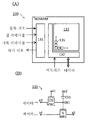
도 1은 마이크로 컨트롤러 유닛(MCU)의 구성예를 나타낸 블록도이다.
도 2의 (A)는 NOSRAM의 구성예를 나타낸 블록도이고, 도 2의 (B)는 메모리 셀의 구성예를 나타낸 회로도이다.
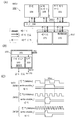
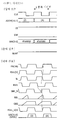
도 3은 MCU의 동작예를 나타낸 타이밍 차트이다.
도 4는 MCU의 동작예를 나타낸 타이밍 차트이다.
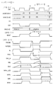
도 5의 (A)는 MCU의 구성예를 나타낸 블록도이고, 도 5의 (B)는 클록 신호 생성 회로의 구성예를 나타낸 블록도이고, 도 5의 (C)는 대기 신호의 구조예를 나타낸 타이밍 차트이다.
도 6의 (A)는 NOSRAM의 구성예를 나타낸 블록도이고, 도 6의 (B)는 메모리 셀의 구성예를 나타낸 회로도이다.
도 7은 MCU의 동작예를 나타낸 타이밍 차트이다.
도 8은 MCU의 동작예를 나타낸 타이밍 차트이다.
도 9의 (A)는 NOSRAM의 구성예를 나타낸 블록도이고, 도 9의 (B)는 메모리 셀의 구성예를 나타낸 회로도이다.
도 10의 (A) 내지 도 10의 (E)는 각각 메모리 셀의 구성예를 도시한 회로도이다.
도 11은 열 드라이버의 구성예를 나타낸 회로도이다.
도 12는 NOSRAM의 판독 동작예를 나타낸 타이밍 차트이다.
도 13은 NOSRAM의 기록 동작예를 나타낸 타이밍 차트이다.
도 14의 (A) 및 도 14의 (B)는 NOSRAM에서의 블록의 구성예를 나타낸 블록도이다.
도 15의 (A)는 전자 부품의 제조 방법예를 나타낸 흐름도이고, 도 15의 (B)는 반도체 웨이퍼의 상면도이고, 도 15의 (C)는 반도체 웨이퍼를 부분적으로 확대한 도면이고, 도 15의 (D)는 칩의 확대도이고, 도 15의 (E)는 전자 부품의 구조예를 도시한 사시 개략도이다.
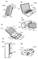
도 16의 (A) 내지 도 16의 (F)는 전자 기기의 구조예를 도시한 것이다.
도 17의 (A)는 OS 트랜지스터의 구조예를 도시한 평면도이고, 도 17의 (B) 및 도 17의 (C)는 도 17의 (A)에서의 OS 트랜지스터의 단면도이다.
도 18의 (A)는 OS 트랜지스터의 구조예를 도시한 평면도이고, 도 18의 (B) 및 도 18의 (C)는 도 18의 (A)에서의 OS 트랜지스터의 단면도이다.
도 19의 (A)는 OS 트랜지스터의 구조예를 도시한 평면도이고, 도 19의 (B) 및 도 19의 (C)는 도 19의 (A)에서의 OS 트랜지스터의 단면도이다.
도 20의 (A)는 OS 트랜지스터의 구조예를 도시한 평면도이고, 도 20의 (B) 및 도 20의 (C)는 도 20의 (A)에서의 OS 트랜지스터의 단면도이다.
도 21의 (A)는 OS 트랜지스터의 구조예를 도시한 평면도이고, 도 21의 (B) 및 도 21의 (C)는 도 21의 (A)에서의 OS 트랜지스터의 단면도이다.
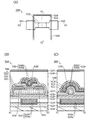
도 22의 (A)는 OS 트랜지스터의 구조예를 도시한 평면도이고, 도 22의 (B) 및 도 22의 (C)는 도 22의 (A)에서의 OS 트랜지스터의 단면도이다.
도 23의 (A)는 OS 트랜지스터의 구조예를 도시한 평면도이고, 도 23의 (B) 및 도 23의 (C)는 도 23의 (A)에서의 OS 트랜지스터의 단면도이다.
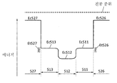
도 24는 OS 트랜지스터의 에너지 밴드도이다.
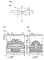
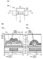
도 25는 MCU의 구조예를 도시한 단면도이다.
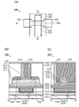
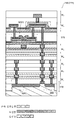
도 26은 MCU의 구조예를 도시한 단면도이다.1 is a block diagram showing a configuration example of a microcontroller unit (MCU).
FIG. 2A is a block diagram showing a configuration example of a NOSRAM, and FIG. 2B is a circuit diagram showing a configuration example of a memory cell.
3 is a timing chart showing an example of the operation of the MCU.
4 is a timing chart showing an example of the operation of the MCU.
5A is a block diagram showing a configuration example of an MCU, FIG. 5B is a block diagram showing a configuration example of a clock signal generation circuit, FIG. 5C shows an example of a structure of a standby signal, Fig.
FIG. 6A is a block diagram showing a configuration example of a NOSRAM, and FIG. 6B is a circuit diagram showing a configuration example of a memory cell.
7 is a timing chart showing an example of the operation of the MCU.
8 is a timing chart showing an example of the operation of the MCU.
FIG. 9A is a block diagram showing a configuration example of a NOSRAM, and FIG. 9B is a circuit diagram showing a configuration example of a memory cell.
10 (A) to 10 (E) are circuit diagrams each showing a configuration example of a memory cell.
11 is a circuit diagram showing a configuration example of a column driver.
12 is a timing chart showing an example of a read operation of the NOSRAM.
13 is a timing chart showing an example of the write operation of the NOSRAM.
14A and 14B are block diagrams showing examples of the configuration of blocks in the NOSRAM.
FIG. 15A is a flow chart showing an example of a manufacturing method of an electronic part, FIG. 15B is a top view of the semiconductor wafer, FIG. 15C is a partially enlarged view of the semiconductor wafer, 15D is an enlarged view of the chip, and FIG. 15E is a perspective view showing an example of the structure of the electronic component.
Figs. 16A to 16F show an example of the structure of an electronic apparatus. Fig.
17A is a plan view showing an example of the structure of an OS transistor, and FIGS. 17B and 17C are cross-sectional views of an OS transistor in FIG. 17A.
18A is a plan view showing an example of the structure of an OS transistor, and FIGS. 18B and 18C are cross-sectional views of an OS transistor in FIG. 18A. FIG.
FIG. 19A is a plan view showing an example of the structure of an OS transistor, and FIGS. 19B and 19C are cross-sectional views of the OS transistor in FIG. 19A.
20A is a plan view showing an example of the structure of an OS transistor, and FIGS. 20B and 20C are cross-sectional views of the OS transistor in FIG. 20A.
21A is a plan view showing an example of the structure of an OS transistor, and FIGS. 21B and 21C are cross-sectional views of the OS transistor in FIG. 21A.
FIG. 22A is a plan view showing an example of the structure of an OS transistor, and FIGS. 22B and 22C are cross-sectional views of the OS transistor in FIG.
23A is a plan view showing an example of the structure of the OS transistor, and FIG. 23B and FIG. 23C are cross-sectional views of the OS transistor in FIG. 23A.
24 is an energy band diagram of the OS transistor.
25 is a cross-sectional view showing an example of the structure of the MCU.
26 is a cross-sectional view showing an example of the structure of the MCU.
이하에서, 본 발명의 실시형태에 대하여 설명하겠다. 또한, 본 명세서에서 설명하는 실시형태들 중 어느 것을 적절히 조합할 수 있다. 또한, 하나의 실시형태에 복수의 구조예(동작예, 사용예, 및 제조 방법예를 포함함)가 제시되는 경우에는, 이들 구조예 중 어느 것을 적절히 조합할 수 있다. 또한, 본 발명은 다양한 상이한 형태로 실시할 수 있고, 본 발명의 취지 및 범위에서 벗어남이 없이, 본 발명의 형태 및 자세한 사항을 다양하게 변경할 수 있다는 것은 통상의 기술자에 의하여 쉽게 이해된다. 따라서, 본 발명은 이하의 실시형태의 기재에 한정하여 해석되지 말아야 한다.Hereinafter, embodiments of the present invention will be described. In addition, any of the embodiments described in this specification can be suitably combined. Further, when a plurality of structural examples (including an operation example, a use example, and a manufacturing method example) are presented in one embodiment, any of these structural examples can be appropriately combined. It will be apparent to those skilled in the art that the present invention may be embodied in many different forms and that the forms and details of the present invention may be modified in various ways without departing from the spirit and scope of the present invention. Therefore, the present invention should not be construed as being limited to description of the following embodiments.
도면에서, 사이즈, 층 두께, 또는 영역 등은 명료화를 위하여 과장되어 있는 경우가 있다. 그러므로, 사이즈, 층 두께, 또는 영역 등은 도시된 스케일에 한정되지 않는다. 도면들이 이상적인 예들의 개략도들이고, 본 발명의 실시형태들이 도면들에 도시된 형상 또는 값에 한정되지 않는다. 예를 들어, 노이즈 또는 타이밍의 어긋남에 의한 신호, 전압, 또는 전류의 변동이 포함될 수 있다.In the drawings, a size, a layer thickness, an area, or the like may be exaggerated for clarity. Therefore, the size, layer thickness, or area, etc. are not limited to the scale shown. The drawings are schematic diagrams of ideal examples, and embodiments of the present invention are not limited to the shapes or values shown in the drawings. For example, fluctuations in signal, voltage, or current due to noise or timing discrepancy may be included.
본 명세서에서, "위", "위쪽", "아래", 및 "아래 쪽" 등의 배치를 설명하는 용어는 도면을 참조하여 구성 요소들 사이의 위치 관계를 설명하기 위하여 편의상 사용되는 경우가 있다. 또한, 구성 요소들의 위치 관계는 각 구성 요소를 기재하는 방향에 따라 적절히 변화된다. 따라서, 본 명세서에서 사용되는 용어에 제한은 없고, 상황에 따라 적절히 설명할 수 있다.In this specification, terms describing the arrangement such as " upper, " " upper, " " lower, " and " lower " and the like are occasionally used to describe a positional relationship among components with reference to the drawings . Further, the positional relationship of the components is appropriately changed according to the direction in which each component is described. Therefore, the term used in the present specification is not limited, and can be suitably explained according to the situation.
블록도에 도시된 회로 블록의 위치 관계는 설명을 위하여 특정되어 있다; 그러므로, 본 발명의 일 형태에 따른 회로 블록의 위치는 이에 한정되지 않는다. 블록도에서 상이한 회로 블록에 의하여 상이한 기능이 실현되도록 도면에 도시되더라도, 실제로는 하나의 회로 블록이 상이한 기능을 실현하여도 좋다. 도면에서의 회로 블록들의 기능은, 설명을 위하여 특정되어 있으며, 특정한 처리를 수행하는 하나의 회로 블록을 도면에 나타내더라도, 복수의 회로 블록이 처리를 수행하기 위하여 실제로 제공될 수 있다.The positional relationship of the circuit blocks shown in the block diagram is specified for illustrative purposes; Therefore, the position of the circuit block according to an aspect of the present invention is not limited thereto. Although shown in the drawings so that different functions are realized by different circuit blocks in the block diagram, one circuit block may actually realize different functions. Although the functions of the circuit blocks in the drawings are specified for the sake of explanation and one circuit block for performing a specific process is shown in the drawings, a plurality of circuit blocks may actually be provided for performing the process.
(실시형태 1)(Embodiment 1)
본 실시형태에서는, OS 메모리가 제공되는 반도체 장치에 대하여 설명한다.In this embodiment, a semiconductor device provided with an OS memory will be described.
<<MCU>><< MCU >>
도 1은 마이크로 컨트롤러 유닛(MCU)의 구성예를 나타낸 것이다. 도 1에 나타낸 MCU(100)는 버스(110), 프로세서 코어(111)(이하에서는, 코어(111)라고 함), 메모리부(112), 클록 생성 회로(115), 및 주변 회로(116)를 포함한다. MCU(100)는 하나의 칩으로 집적된 반도체 장치이다.1 shows a configuration example of a microcontroller unit (MCU). 1 includes a bus 110, a processor core 111 (hereinafter, referred to as a core 111), a
클록 생성 회로(115)는 MCU(100)에서 사용되는 클록 신호를 생성하는 기능을 갖는다. 주변 회로(116)의 기능에 특별한 제한은 없다. 주변 회로(116)에는, MCU(100)의 용도에 따라 다양한 기능 회로가 제공된다. 기능 회로의 예에는, 전원 회로, 전원 관리 유닛, 타이머 장치, 인터럽트 컨트롤러, 입출력 포트, 아날로그-디지털 컨버터(ADC), 콤퍼레이터, 및 연산 증폭기가 포함된다.The
메모리부(112)는 NOSRAM(120) 및 메모리(121)를 포함한다. "NOSRAM"(등록 상표)은 OS 메모리의 일종이다. NOSRAM에 대해서는 나중에 설명하겠다. 메모리(121)는 재기록할 수 있기만 하면 어느 메모리이어도 좋고, 예를 들어, SRAM, 플래시 메모리, 강유전 RAM(FeRAM), 자기 저항 RAM(MRAM), 저항 RAM(ReRAM), 또는 상변화 RAM(PRAM)이다.The
메모리부(112)에 메모리(121)를 반드시 제공할 필요는 없다. 또는, 복수의 메모리(121)를 메모리부(112)에 제공하여도 좋다. 예를 들어, SRAM 및 플래시 메모리를 메모리부(112)에 제공하여도 좋다. 판독 전용 메모리(ROM)를 메모리부(112)에 제공하여도 좋다.It is not always necessary to provide the
코어(111)는 버스(110)를 통하여 메모리부(112) 및 주변 회로(116)와 데이터를 교환한다. 코어(111)로부터의 제어 신호는 버스(110)에 입력된다. 버스(110)는 제어되는 회로 블록로 제어 신호를 송신한다. 제어 신호는 이네이블 신호 및 어드레스 신호를 포함한다.The
NOSRAM(120), 메모리(121), 및 주변 회로(116)는 각각 대기 신호를 발행하는 기능을 갖는다. 대기 신호는 액세스의 지연을 코어(111)에 요구하는 신호이다. 버스(110)에 입력되는 대기 신호는 코어(111)에 전송된다.The
<NOSRAM><NOSRAM>
도 2의 (A)는 NOSRAM(120)의 구성예를 나타낸 블록도이다. 도 2의 (A)에 나타낸 NOSRAM(120)은 제어부(131), 드라이버부(132), 및 셀 어레이(133)를 포함한다.FIG. 2A is a block diagram showing an example of the configuration of the
제어부(131)는 NOSRAM(120)의 동작 전체를 제어하는 기능을 갖는 논리 회로이다. 제어부(131)는 칩 이네이블 신호 및 기록 이네이블 신호에 대한 논리 연산을 수행하고, 코어(111)의 액세스가 기록 액세스인지 판독 액세스인지를 결정한다. 제어부(131)는 논리 연산을 바탕으로 드라이버부(132)의 제어 신호를 생성한다. 액세스가 기록 액세스라면, 제어부(131)는 대기 신호를 발행하고, 버스(110)로 대기 신호를 송신한다. 코어(111)가 대기 신호를 수신하면, 다음 액세스의 실행을 지연시킨다.The
기록 이네이블 신호는 코어(111)에 의하여 생성된다. 칩 이네이블 신호는 버스(110)에 의하여 생성된다. 버스(110)는 코어(111)로부터 출력되는 어드레스 신호 및 기록 이네이블 신호를 바탕으로 칩 이네이블 신호를 생성한다.The write enable signal is generated by the
드라이버부(132)는 셀 어레이(133)에 데이터를 기록하고 셀 어레이(133)로부터 데이터를 판독하는 회로이다. 예를 들어, 드라이버부(132)는 어드레스 신호를 디코딩하기 위한 디코더, 워드선 드라이버, 판독 회로, 및 기록 회로 등을 포함한다.The
메모리 셀(135)은 셀 어레이(133)에 매트릭스로 배치된다. 도 2의 (B)는 메모리 셀(135)의 구성예를 도시한 것이다. 여기서, 메모리 셀(135)은 2T형 게인 셀이다. 메모리 셀(135)은 트랜지스터(MW1), 트랜지스터(MR1), 용량 소자(CS1), 노드(SN1), 및 노드(a1) 내지 노드(a5)를 포함한다. 트랜지스터(MW1)는 기록 트랜지스터로서 기능하는 OS 트랜지스터이다. 트랜지스터(MR1)는 판독 트랜지스터이고, 도 2의 (B)의 예에서는 n-채널 Si 트랜지스터이다. 노드(SN1)는 데이터 유지 노드이고, 용량 소자(CS1)는 노드(SN1)의 전하를 유지하기 위한 저장 용량 소자이다.The
OS 트랜지스터는 오프 상태 전류가 매우 낮기 때문에, 메모리 셀의 트랜지스터로서 사용되는 것이 바람직하다. 여기서, 오프 상태 전류란 오프 상태에서 트랜지스터의 소스와 드레인 사이를 흐르는 전류를 말한다. n-채널 트랜지스터의 경우, 예를 들어, 트랜지스터의 문턱 전압이 0V 내지 2V 정도라면, 게이트와 소스 사이의 전압이 음일 때의 소스와 드레인 사이를 흐르는 전류를 오프 상태 전류라고 할 수 있다. 매우 낮은 오프 상태 전류는 예를 들어, 채널 폭 1μm당 오프 상태 전류가 100zA(z는 젭토를 나타내고, 10-21의 인수(factor)를 나타냄) 이하인 것을 의미한다. 오프 상태 전류는 가능한 한 낮은 것이 바람직하기 때문에, 정규화된 오프 상태 전류가 10zA/μm 이하 또는 1zA/μm) 이하인 것이 바람직하고, 10yA/μm(y는 욕토를 나타내고, 10-24의 인수를 나타냄) 이하인 것이 더 바람직하다.The OS transistor is preferably used as a transistor of the memory cell because the off-state current is very low. Here, the off-state current refers to a current flowing between the source and the drain of the transistor in the off-state. In the case of an n-channel transistor, for example, if the threshold voltage of the transistor is about 0 V to 2 V, a current flowing between the source and the drain when the voltage between the gate and the source is negative can be called an off-state current. The very low off-state current means, for example, that the off-state current per 1 μm channel width is less than or equal to 100 zA (where z represents a factor and represents a factor of 10 -21 ). Off-state current is a low because it is desirable, and it is normalized off-state current is 10zA / μm or less, or 1zA / μm) or less preferably, 10yA / μm (y denotes a possible yokto, represents a factor of 10 -24) Or less.
산화물 반도체는 3.0eV 이상의 밴드 갭을 갖는다; 따라서, OS 트랜지스터는 열 여기로 인한 누설 전류가 낮고, 상술한 바와 같이 매우 낮은 오프 상태 전류를 갖는다. OS 트랜지스터의 채널 형성 영역으로서 사용되는 산화물 반도체는 인듐(In) 및 아연(Zn) 중 적어도 한쪽을 함유하는 산화물 반도체인 것이 바람직하다. 이러한 산화물 반도체의 대표적인 예에는 In-M-Zn 산화물(원소 M은 예를 들어, Al, Ga, Y, 또는 Sn임)이 포함된다. 전자 공여체로서 기능하는 수분 또는 수소 등의 불순물을 저감하고, 산소 결손도 저감함으로써, i형(진성) 또는 실질적으로 i형의 산화물 반도체를 얻을 수 있다. 여기서는, 이러한 산화물 반도체를 고순도화된 산화물 반도체라고 할 수 있다. 고순도화된 산화물 반도체를 사용함으로써, 채널 폭으로 정규화된 OS 트랜지스터의 오프 상태 전류를 수yA/μm 내지 수zA/μm로 낮게 할 수 있다. OS 트랜지스터 및 산화물 반도체에 대해서는 실시형태 5 및 실시형태 6에서 설명하겠다.The oxide semiconductor has a band gap of 3.0 eV or more; Thus, the OS transistor has a low leakage current due to thermal excitation and has a very low off-state current as described above. The oxide semiconductor used as the channel forming region of the OS transistor is preferably an oxide semiconductor containing at least one of indium (In) and zinc (Zn). Representative examples of such oxide semiconductors include In- M- Zn oxide (element M is, for example, Al, Ga, Y, or Sn). An i-type (intrinsic) or substantially i-type oxide semiconductor can be obtained by reducing impurities such as moisture or hydrogen which function as an electron donor and reducing oxygen deficiency. Here, such an oxide semiconductor can be regarded as an oxide semiconductor of high purity. By using a high-purity oxide semiconductor, the off-state current of the OS transistor normalized to the channel width can be reduced to several yA / μm to several zA / μm. The OS transistor and the oxide semiconductor will be described in the fifth embodiment and the sixth embodiment.
메모리 셀(135)에 데이터를 기록하기 위해서는, 노드(a3)에 데이터를 입력한다. 노드(a1)를 "H"로 설정하여 트랜지스터(MW1)를 온으로 한다; 그 결과, 노드(a3)의 데이터가 노드(SN1)에 기록된다. 트랜지스터(MW1)를 오프로 하고 노드(SN1)를 플로팅 상태로 함으로써, 데이터 기록이 완료된다.To write data in the
노드(a4)의 전압을 데이터로서 판독한다. 데이터는 예를 들어, 이하와 같이 판독된다. 노드(a5)의 전위를 고정한다. 노드(a4)를 프리차지하고 나서, 플로팅 상태로 한다. 노드(SN1)의 전압에 따른 드레인 전류가 트랜지스터(MR1)에 흐른다. 그러므로, 노드(a4)의 전압이 노드(SN1)의 전압에 따라 변화된다.And reads the voltage of the node a4 as data. The data is read, for example, as follows. And fixes the potential of the node a5. After the node a4 is precharged, it is brought into a floating state. A drain current corresponding to the voltage of the node SN1 flows in the transistor MR1. Therefore, the voltage of the node a4 is changed in accordance with the voltage of the node SN1.
오프 상태 전류가 매우 낮다는, OS 트랜지스터의 특징에 의하여, 노드(SN1)의 전압의 저하를 방지할 수 있고, 데이터를 유지하기 위하여 전력을 거의 소비하지 않는다; 그러므로, 메모리 셀(135)은 오랫동안 데이터를 유지할 수 있다, 즉, 비휘발성이다. 본 명세서 등에서, 게인 셀로 구성되는 셀 어레이를 갖는 OS 메모리는 NOSRAM(nonvolatile oxide semiconductor RAM)이라고 불린다. NOSRAM은 장기간의 데이터 유지에 더하여 다음과 같은 특징을 갖는다.By virtue of the characteristics of the OS transistor that the off-state current is very low, it is possible to prevent the voltage of the node SN1 from dropping and to consume little power to hold data; Therefore, the
용량 소자의 충방전에 의하여 데이터를 재기록하기 때문에, 이론상, NOSRAM의 재기록 동작 횟수에 제한은 없고, 낮은 에너지로 데이터를 NOSRAM에 기록하거나, NOSRAM으로부터 판독할 수 있다. 메모리 셀의 간단한 회로 구성에 의하여, NOSRAM의 용량을 용이하게 증가시킬 수 있다. 그러므로, NOSRAM을 탑재함으로써, 고용량 메모리부를 포함하는, 전력이 낮은 MCU를 제공할 수 있다. 따라서, NOSRAM은 재기록 내성이 높기 때문에, 고용량 메모리로서 적합하게 사용된다. 그러나, NOSRAM의 메모리 셀은 간단한 회로 구성을 갖기 때문에, 메모리 모듈로서의 NOSRAM의 성능은 OS 트랜지스터의 전기 특성에 크게 영향을 받는다.The data is rewritten by charge / discharge of the capacitive element. Therefore, theoretically, the number of rewriting operations of the NOSRAM is not limited, and data can be written into or read from the NOSRAM with low energy. The capacity of the NOSRAM can be easily increased by a simple circuit configuration of the memory cell. Therefore, by mounting the NOSRAM, it is possible to provide a low power MCU including a high capacity memory portion. Therefore, NOSRAM is suitably used as a high capacity memory because of its high rewrite resistance. However, since the memory cell of the NOSRAM has a simple circuit configuration, the performance of the NOSRAM as the memory module is greatly influenced by the electrical characteristics of the OS transistor.
OS 트랜지스터는 Si 트랜지스터보다 온 상태 전류가 낮다. 데이터를 OS 트랜지스터의 스위칭 동작에 의하여 메모리 셀에 기록하기 때문에, NOSRAM의 메모리 셀의 기록 속도는 NOSRAM의 메모리 셀의 판독 속도보다 느리다. 그러므로, NOSRAM을 포함하는 MCU의 클록 주파수는 NOSRAM의 기록 속도에 의하여 제한된다. 바꿔 말하면, 동작 주파수가 높은 MCU에 NOSRAM을 탑재하는 것은 매우 어렵다. 본 실시형태는 이러한 문제가 없는 MCU를 제공할 수 있다.OS transistors have lower on-state current than Si transistors. Since the data is written to the memory cell by the switching operation of the OS transistor, the writing speed of the memory cell of the NOSRAM is slower than the reading speed of the memory cell of the NOSRAM. Therefore, the clock frequency of the MCU including the NOSRAM is limited by the recording speed of the NOSRAM. In other words, it is very difficult to mount a NOSRAM in an MCU having a high operating frequency. The present embodiment can provide an MCU without such a problem.
구체적으로, 도 1에 나타낸 MCU(100)에서는, 코어(111)가 NOSRAM(120)으로부터의 대기 신호를 수신하면, 코어(111)는 메모리부(112)의 기록 사이클에 (n+1)클록 사이클(n은 1 이상의 정수임)을 할당한다. MCU(100)의 동작예에 대해서는 도 3 및 도 4를 참조하여 이하에서 설명한다.More specifically, in the
<<MCU의 동작예>><< Operation example of MCU >>
도 3 및 도 4는 각각 메모리부(112)에 대한 코어(111)의 액세스를 나타낸 타이밍 차트이다. 도 3 및 도 4에서, CY0 및 CY1 등은 클록 사이클을 나타낸다. 또한, "_o"는 버스(110)로의 출력 신호를 나타내고, "_i"는 버스(110)로부터의 입력 신호를 나타낸다. 예를 들어, "Address_o"는 코어(111)가 버스(110)에 출력하는 어드레스 신호를 나타내고, "Address_i"는 버스(110)로부터 NOSRAM(120)에 입력되는 어드레스 신호를 나타낸다. NOSRAM(120)으로부터 판독되는 데이터는 코어(111)에 입력된다. 코어(111)가 출력한 데이터는 NOSRAM(120)에 기록된다.3 and 4 are timing charts showing the access of the core 111 to the
도 3 및 도 4는 어드레스(A) 및 어드레스(B)에 대한 액세스를 상세히 나타낸 것이다. 도 3 및 도 4에서 다른 동작에 관한 어드레스, 및 데이터는 "X"라고 약기된다. 어드레스(A) 및 어드레스(B)는 NOSRAM(120)의 어드레스이고, 어드레스(C) 및 어드레스(D)는 메모리(121)의 어드레스이다. 코어(111)는 어드레스(A)로부터 데이터(A)를 판독하고, 어드레스(B)에 데이터(B)를 기록한다.Figs. 3 and 4 show details of the access to the address A and the address B. Fig. The addresses and data relating to other operations in Figs. 3 and 4 are abbreviated as " X ". The addresses A and B are the addresses of the
(참조예)(Reference example)
우선, NOSRAM(120)이 대기 신호를 생성하는 기능을 갖지 않는 경우의 MCU(100)의 동작예를 참조예로서 설명한다. 도 4는 코어(111)의 NOSRAM(120)에 대한 액세스를 나타낸 타이밍 차트이다.First, an operation example of the
클록 사이클(CY1)에서, 코어(111)는 버스(110)에 어드레스(A) 및 "L"의 기록 이네이블 신호를 출력한다. 다음에, 클록 사이클(CY2)에서, 어드레스(A), "L"의 기록 이네이블 신호, 및 "H"의 칩 이네이블 신호를 NOSRAM(120)에 입력한다. 기록 이네이블 신호가 "L"이기 때문에, NOSRAM(120)은 어드레스(A)에 저장된 데이터(A)를 판독한다. 데이터(A)는 버스(110)를 통하여 코어(111)에 입력된다.In the clock cycle CY1, the
또한, 코어(111)가 어드레스(A)를 발행한 후, 코어(111)는 클록 사이클(CY2)에서 버스(110)에 어드레스(B) 및 "H"의 기록 이네이블 신호를 출력하고, 클록 사이클(CY3)에서 버스(110)에 데이터(B)를 출력한다. 클록 사이클(CY3)에서, 어드레스(B), 데이터(B), "H"의 기록 이네이블 신호, 및 "H"의 칩 이네이블 신호를 NOSRAM(120)에 입력한다. 클록 사이클(CY3)에서, NOSRAM(120)은 데이터(B)를 어드레스(B)에 기록한다.After the core 111 issues the address A, the
클록 사이클(CY3)에서, 코어(111)는 버스(110)에 어드레스(C)를 출력한다. 어드레스(C)는 메모리(121)의 어드레스이기 때문에, 버스(110)는 클록 사이클(CY4)에서 NOSRAM(120)에 "L"의 칩 이네이블 신호를 출력한다.In the clock cycle CY3, the
도 4의 예에서는, NOSRAM(120)의 기록 사이클 및 판독 사이클 각각에는 1클록 사이클이 할당된다. 그러므로, 1클록 사이클 시간을 NOSRAM(120)의 기록 사이클 시간보다 짧게 할 수 없다. 예를 들어, NOSRAM(120)의 데이터 기록 사이클 시간이 20ns인 경우, MCU(100)의 동작 주파수를 50MHz(1클록 사이클 시간=20ns)보다 높게 할 수 없다.In the example of FIG. 4, one clock cycle is allocated to each of the write cycle and the read cycle of the
본 실시형태는 동작 주파수가 NOSRAM의 기록 사이클 시간에 의하여 제한되지 않는 MCU를 제공할 수 있고, 이에 대하여 도 3의 타이밍 차트를 참조하여 설명한다. 도 3은 NOSRAM(120)에 대한 코어(111)의 액세스를 나타낸 타이밍 차트이다.The present embodiment can provide an MCU whose operating frequency is not limited by the write cycle time of the NOSRAM, and this will be described with reference to the timing chart of Fig. 3 is a timing chart showing the access of the core 111 to the
도 3에서, "L"의 대기 신호는 액티브이고, "H"의 대기 신호는 비액티브이다.In Fig. 3, the standby signal of " L " is active and the standby signal of " H " is inactive.
판독 액세스의 동작은 도 4에서의 참조예의 동작과 비슷하다. 코어(111)는 클록 사이클(CY1)에서 어드레스(A)를 발행하고, NOSRAM(120)은 클록 사이클(CY2)에서 데이터(A)를 판독한다. NOSRAM(120)의 판독 동작을 고속으로 수행할 수 있다; 그러므로, 코어(111)가 어드레스를 발행하는 클록 사이클에서 NOSRAM(120)이 판독한 데이터가 코어(111)에 전달된다.The operation of the read access is similar to that of the reference example in Fig.
기록 액세스의 동작은 도 4에서의 참조예의 동작과 상이하다. 클록 사이클(CY2)에서, 코어(111)는 어드레스(B) 및 "H"의 기록 이네이블 신호를 버스(110)에 출력한다. 클록 사이클(CY3)에서, 어드레스(B), "H"의 기록 이네이블 신호, 및 "H"의 칩 이네이블 신호를 NOSRAM(120)에 입력한다. 클록 신호의 상승 시에서의 기록 이네이블 신호는 "H"이기 때문에, NOSRAM(120)은 "L"의 대기 신호를 출력한다.The operation of the write access differs from the operation of the reference example in Fig. In the clock cycle CY2, the
클록 사이클(CY4)에서, 클록 신호의 상승 시에서의 대기 신호의 논리는 "L"이다; 그러므로, 코어(111)는 메모리부(112)에 대한 액세스의 요구를 지연시키고, 클록 사이클(CY3)과 동일한 처리를 실행한다. 따라서, NOSRAM(120)에서는, 어드레스(B)로의 데이터(B)의 기록을 2클록 사이클(CY3 및 CY4)에서 수행할 수 있다.In the clock cycle CY4, the logic of the wait signal at the rise of the clock signal is " L "; Therefore, the core 111 delays the access request to the
클록 사이클(CY5)에서, 클록 신호의 상승 시에서의 대기 신호의 논리는 "H"이다; 그러므로, 코어(111)는 지연된 액세스 요구를 실행한다. 도 3의 예에서, 코어(111)는 어드레스(D)를 발행한다.In the clock cycle CY5, the logic of the wait signal at the rise of the clock signal is " H "; Therefore, the
도 3의 예에서는 NOSRAM(120)의 기록 사이클에 2클록 사이클을 할당하지만, 기록 사이클에 할당되는 클록 사이클의 수는 2개에 한정되지 않는다. (n+1)클록 사이클(n은 1 이상의 정수임)을 NOSRAM(120)의 기록 사이클에 할당할 수 있다. 이 경우, 대기 신호가 "L"인 기간은 n클록 사이클 시간에 상당한다.In the example of FIG. 3, two clock cycles are allocated to the write cycle of the
NOSRAM(120)의 기록 사이클 시간이 20ns인 경우를 상정한다. 클록 신호의 주파수가 100MHz(클록 사이클 시간=10ns)인 경우, 1클록 사이클 동안 액티브 대기 신호가 발행되고, 기록 사이클에 2클록 사이클이 할당된다. 클록 신호의 주파수가 200MHz(클록 사이클 시간=5ns)인 경우, 3클록 사이클 동안 액티브 대기 신호가 발행되고, 기록 사이클에 4클록 사이클이 할당된다.It is assumed that the write cycle time of the
또한, "H"의 대기 신호는 NOSRAM(120)이 코어(111)의 액세스를 수신할 수 있는 것을 가리키고, "L"의 대기 신호는 NOSRAM(120)이 코어(111)의 액세스를 수신할 수 없는 것을 가리킨다; 그러므로, 대기 신호를 준비 신호로 간주할 수 있다.A wait signal of " H " indicates that
프로세서 코어의 동작 주파수는 NOSRAM의 기록 사이클 시간에 의하여 제한되지 않는다. 즉, NOSRAM의 성능에 따른 동작이 가능하다; 그러므로, MCU의 시스템 전체의 성능을 유지하면서, MCU는 전력이 낮은 NOSRAM을 포함할 수 있다. MCU는 NOSRAM을 내장할 수 있기 때문에, MCU를 고용량 메모리부를 갖는, 성능이 높고 전력이 낮은 MCU로 할 수 있다.The operating frequency of the processor core is not limited by the write cycle time of the NOSRAM. That is, the operation according to the performance of the NOSRAM is possible; Therefore, while maintaining the overall system performance of the MCU, the MCU may include a low power NOSRAM. Since the MCU can incorporate the NOSRAM, the MCU can be a high-performance, low-power MCU with a high capacity memory.
본 실시형태에서는, MCU를 예로서 사용하여 발명의 일 형태에 대하여 설명하였다. 그러나, 본 실시형태의 적용은 MCU에 한정되지 않고, 본 실시형태는 프로세서 코어 및 메모리부를 갖는 다양한 프로세서에 적용할 수 있다.In the present embodiment, an embodiment of the invention has been described using the MCU as an example. However, the application of the present embodiment is not limited to the MCU, and the present embodiment can be applied to various processors having a processor core and a memory section.
(실시형태 2)(Embodiment 2)
본 실시형태에서는, OS 메모리가 제공된 반도체 장치의 예로서 MCU에 대하여 설명한다. 본 실시형태의 MCU에서는, NOSRAM의 기록 사이클 시간을 MCU에 사용된 클록 신호의 주파수에 따라 변경할 수 있다.In the present embodiment, an MCU is described as an example of a semiconductor device provided with an OS memory. In the MCU of the present embodiment, the write cycle time of the NOSRAM can be changed in accordance with the frequency of the clock signal used in the MCU.
<<MCU>><< MCU >>
도 5의 (A)는 MCU의 구성예를 나타낸 것이다. 도 5의 (A)에 나타낸 MCU(102)는 버스(150), 프로세서 코어(151)(이하에서는, 코어(151)라고 함), 메모리부(152), 클록 생성 회로(155), 및 주변 회로(156)를 포함한다. MCU(102)는 하나의 칩으로 집적된 반도체 장치이다.5 (A) shows an example of the configuration of the MCU. The
코어(151)는 버스(150)를 통하여 메모리부(152) 및 주변 회로(156)와 데이터를 교환한다. 코어(151)로부터의 제어 신호는 버스(150)에 입력된다. 버스(150)는 제어되는 회로 블록으로 제어 신호를 송신한다. 제어 신호는 이네이블 신호 및 어드레스 신호를 포함한다.The
주변 회로(156)의 기능에 특별한 제한은 없다. 주변 회로(156)에는, MCU(102)의 용도에 따라 다양한 기능 회로가 제공된다. 기능 회로의 예에는, 전원 회로, 전원 관리 유닛, 타이머 장치, 인터럽트 컨트롤러, 입출력 포트, 아날로그-디지털 컨버터(ADC), 콤퍼레이터, 및 연산 증폭기가 포함된다.The function of the
메모리부(152)는 NOSRAM(170) 및 메모리(171)를 포함한다. 메모리(171)는 재기록 할 수 있기만 하면 어느 메모리이어도 좋고, 예를 들어, SRAM, 플래시 메모리, 강유전 RAM(FeRAM), 자기 저항 RAM(MRAM), 저항 RAM(ReRAM), 또는 상변화 RAM(PRAM)이다.The
메모리부(152)에 메모리(171)를 반드시 제공할 필요는 없다. 또는, 복수의 메모리(171)를 메모리부(152)에 제공하여도 좋다. 예를 들어, SRAM 및 플래시 메모리를 메모리부(152)에 제공하여도 좋다. 판독 전용 메모리(ROM)를 메모리부(152)에 제공하여도 좋다.It is not always necessary to provide the
NOSRAM(170), 메모리(171), 및 주변 회로(156)는 각각 대기 신호를 발행하는 기능을 갖는다. 대기 신호는 액세스의 지연을 코어(151)에 요구하는 신호이다. 버스(150)에 입력되는 대기 신호는 코어(151)에 전송된다.The
클록 생성 회로(155)는 MCU(102)에서 사용되는 클록 신호를 생성하는 기능을 갖는다. 클록 생성 회로(155)는 클록 생성 회로(155)에 저장되는, 주파수를 설정하기 위한 데이터를 바탕으로 클록 주파수를 변경하는 기능을 갖는다. 주파수를 설정하기 위한 데이터의 재기록은 코어(151)에 의하여 수행된다. 도 5의 (B)는 클록 생성 회로(155)의 구성예를 나타낸 것이다.The
<클록 생성 회로><Clock Generation Circuit>
클록 생성 회로(155)는 설정 레지스터(161), 클록 생성기(162), 및 논리부(163)를 포함한다. 설정 레지스터(161)는 클록 주파수를 설정하기 위한 데이터(FQ)(이하에서는, 데이터(FQ)라고 함)를 저장하는 기능을 갖는다. 설정 레지스터(161)의 데이터(FQ)는 코어(151)에 의하여 제어됨으로써 재기록될 수 있다. 설정 레지스터(161)는 데이터(FQ)를 클록 생성기(162) 및 논리부(163)에 출력한다.The
클록 생성기(162)는 데이터(FQ)에 따른 주파수를 갖는 클록 신호를 생성한다. 클록 생성기(162)에 의하여 생성되는 클록 신호는 MCU(102)에서 사용된다.The
논리부(163)는 데이터(FQ)를 바탕으로 신호(WCY)를 생성하는 기능을 갖는다. 신호(WCY)는 버스(150)를 통하지 않고 NOSRAM(170)에 입력된다. 신호(WCY)는 NOSRAM(170)의 기록 사이클에 할당되는 클록 사이클의 수를 설정하는 기능을 갖는다.The
클록 신호의 주파수를 클록 생성 회로(155)에 의하여 변경할 수 있기 때문에, MCU(102)에서의 고성능화 및 저소비전력화를 달성할 수 있다. 더 빠른 처리가 필요할 때에 클록 주파수를 증가시킨다. 전력을 저감하기 위해서는(예를 들어, 배터리에 의한 구동 시에는), 클록 주파수를 저감할 수 있다.The frequency of the clock signal can be changed by the
<NOSRAM><NOSRAM>
도 6의 (A)는 NOSRAM(170)의 구성예를 나타낸 블록도이다. 도 6의 (A)에 나타낸 NOSRAM(170)은 제어부(181), 드라이버부(182), 및 셀 어레이(183)를 포함한다.6 (A) is a block diagram showing a configuration example of the
제어부(181)는 NOSRAM(170)의 동작 전체를 제어하는 기능을 갖는 논리 회로이다. 제어부(181)는 칩 이네이블 신호 및 기록 이네이블 신호에 대한 논리 연산을 수행하고, 코어(151)의 액세스가 기록 액세스인지 판독 액세스인지를 결정하는 기능, 칩 이네이블 신호, 기록 이네이블 신호, 및 신호(WCY)에 대한 논리 연산을 수행하고, 드라이버부(182)의 제어 신호를 생성하는 기능, 및 기록 이네이블 신호 및 신호(WCY)를 바탕으로 대기 신호를 발행하는 기능을 갖는다.The
코어(151)로부터의 기록 액세스에 의하여, 제어부(181)는 대기 신호를 발행하고, 버스(150)로 대기 신호를 송신한다. 코어(151)가 대기 신호를 수신하면, 코어(151)는 다음의 액세스의 실행을 지연시킨다.By the write access from the
기록 이네이블 신호는 코어(151)에 의하여 생성된다. 칩 이네이블 신호는 버스(150)에 의하여 생성된다. 버스(150)는 코어(151)로부터 출력되는 어드레스 신호 및 기록 이네이블 신호를 바탕으로 칩 이네이블 신호를 생성한다.The write enable signal is generated by the
드라이버부(182)는 셀 어레이(183)에 데이터를 기록하고 셀 어레이(183)로부터 데이터를 판독하는 회로이다. 예를 들어, 드라이버부(182)는 어드레스 신호를 디코딩하기 위한 디코더, 워드선 드라이버, 판독 회로, 및 기록 회로 등을 포함한다.The
메모리 셀(185)은 셀 어레이(183)에 매트릭스로 배치된다. 도 6의 (B)는 메모리 셀(185)의 구성예를 도시한 것이다. 메모리 셀(185)의 회로 구성은 도 2의 (B)에서의 메모리 셀(135)의 회로 구성과 동일하다.The
실시형태 1에서 설명한 바와 같이, OS 트랜지스터는 Si 트랜지스터보다 온 상태 전류가 낮기 때문에, NOSRAM을 내장하는 MCU의 클록 주파수는 NOSRAM의 기록 속도에 의하여 제한된다. 본 실시형태는 이러한 문제를 해결하여 동작 주파수가 NOSRAM의 기록 속도에 의하여 제한되지 않는 MCU를 제공할 수 있다.As described in
구체적으로는, 설정 레지스터(161)의 데이터(FQ)를 코어(151)에 의하여 재기록함으로써, 클록 주파수 및 NOSRAM(170)의 기록 사이클 시간을 최적화할 수 있다. 표 1은 데이터(FQ)에 따라 설정되는 클록 주파수 및 기록 사이클 시간의 예를 나타낸 것이다. 여기서, 클록 주파수를 10MHz, 50MHz, 100MHz, 및 200MHz 중 어느 것으로 설정한다.Concretely, the clock frequency and the write cycle time of the
[표 1][Table 1]
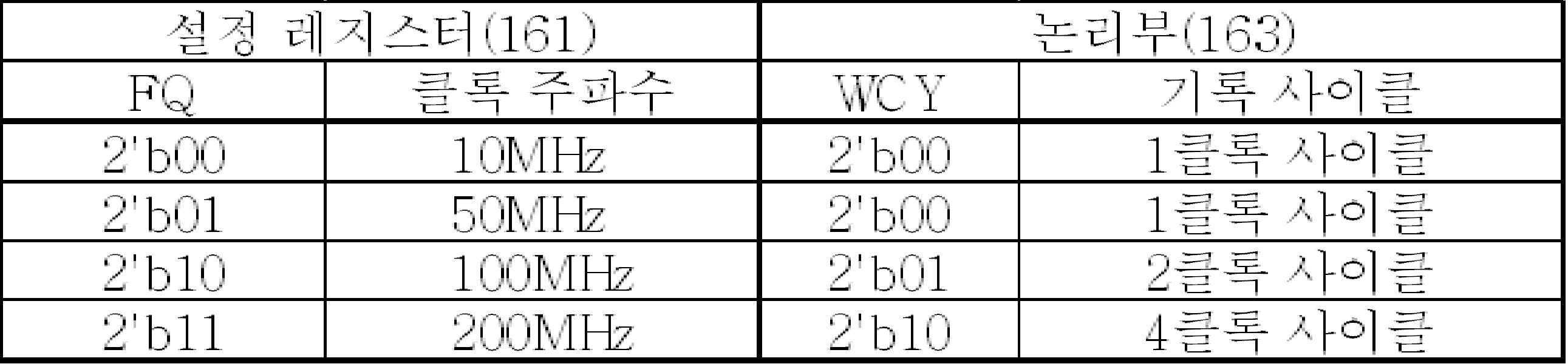
데이터(FQ)는 2비트 데이터이다. 코어(151)가 설정 레지스터(161)에 2'b00를 기록하면, 클록 생성기(162)는 10MHz의 클록 신호를 생성하는 한편, 코어(151)가 설정 레지스터(161)에 2'b11을 기록하면, 클록 생성기(162)는 200MHz의 클록 신호를 생성한다.The data FQ is 2-bit data. When the core 151 records 2'b00 in the
표 1은 논리부(163)의 진리표에 대응한다. 여기서는, NOSRAM(170)의 기록 사이클 시간이 20ns로 최적화되는 것을 상정한다. 또한, 20ns는 클록 주파수가 50MHz인 경우의 1클록 사이클 시간에 상당한다. 클록 주파수가 50MHz보다 높은 경우, NOSRAM(170)의 기록 사이클에 2개 이상의 클록 사이클을 할당할 필요가 있다. 따라서, MCU(102)에서, NOSRAM(170)의 기록 사이클에 필요한 클록 사이클의 수는 신호(WCY)에 의하여 제어된다.Table 1 corresponds to the truth table of
2'b01이 설정 레지스터(161)에 기록되면, 논리부(163)는 NOSRAM(170)에 2'b00의 신호(WCY)를 출력하는 한편, 2'b10이 설정 레지스터(161)에 기록되면, 논리부(163)는 NOSRAM(170)에 2'b01의 신호(WCY)를 출력한다. NOSRAM(170)이 기록 이네이블 신호를 수신하면, NOSRAM(170)은 신호(WCY)의 데이터를 바탕으로 대기 신호를 생성한다. 여기서, 신호(WCY)의 값은 NOSRAM(170)이 대기 신호를 발행하는 클록 사이클 시간을 나타낸다.When the 2'b01 is written in the
표 1의 예에서 데이터(FQ) 및 신호(WCY)의 비트 폭은 각각 2비트이지만, 본 발명의 일 형태는 이에 한정되지 않는다. 데이터(FQ)의 비트 폭을 클록 주파수의 사용 수에 따라 결정할 수 있다. 신호(WCY)의 비트 폭을 클록 주파수 및 NOSRAM(170)의 기록 특성에 따라 결정할 수 있다.In the example of Table 1, the bit widths of the data (FQ) and the signal (WCY) are each 2 bits, but one form of the present invention is not limited thereto. The bit width of the data FQ can be determined according to the number of clock frequencies used. The bit width of the signal WCY can be determined according to the clock frequency and the recording characteristic of the
<<MCU의 동작예>><< Operation example of MCU >>
MCU(102)의 동작예에 대하여 도 7 및 도 8을 참조하여 이하에서 설명한다. 도 7 및 도 8은 각각 메모리부(152)에 대한 코어(151)의 액세스를 나타낸 타이밍 차트이다. 도 7의 예에서 클록 주파수는 50MHz이고, 도 8의 예에서는 100MHz이다.An operation example of the
도 7 및 도 8에서, CY0 및 CY1 등은 클록 사이클을 나타낸다. 또한, "_o"는 버스(150)로의 출력 신호를 나타내고, "_i"는 버스(150)로부터의 입력 신호를 나타낸다. 예를 들어, "Address_o"는 코어(151)가 버스(110)에 출력하는 어드레스 신호를 나타내고, "Address_i"는 버스(150)로부터 NOSRAM(170)에 입력되는 어드레스 신호를 나타낸다. NOSRAM(170)으로부터 판독되는 데이터는 코어(151)에 입력된다. 코어(151)가 출력하는 데이터는 NOSRAM(170)에 기록된다.In Figs. 7 and 8, CY0 and CY1 and the like represent clock cycles. "_O" represents an output signal to the bus 150, and "_i" represents an input signal from the bus 150. For example, "Address_o" indicates an address signal that the
도 7 및 도 8은 어드레스(A) 및 어드레스(B)에 대한 액세스를 상세히 나타낸 것이다. 도 7 및 도 8에서 다른 동작에 관한 어드레스, 및 데이터는 "X"라고 약기된다. 어드레스(A) 및 어드레스(B)는 NOSRAM(170)의 어드레스이고, 어드레스(C) 및 어드레스(D)는 메모리(171)의 어드레스이다. 코어(151)는 어드레스(A)로부터 데이터(A)를 판독하고, 어드레스(B)에 데이터(B)를 기록한다.Figs. 7 and 8 show details of the access to the address A and the address B. Fig. Addresses and data relating to other operations in Figs. 7 and 8 are abbreviated as " X ". The addresses A and B are the addresses of the
여기서, "L"의 대기 신호는 액티브이고, "H"의 대기 신호는 비액티브이다.Here, the standby signal of "L" is active and the standby signal of "H" is inactive.
(동작예 1)(Operation Example 1)
도 7을 참조하여, NOSRAM(170)의 기록 사이클 시간이 1클록 사이클 시간에 상당하는 경우의 MCU(102)의 동작예에 대하여 설명한다.An operation example of the
클록 사이클(CY1)에서, 코어(151)는 버스(150)에 어드레스(A) 및 "L"의 기록 이네이블 신호를 출력한다. 다음에, 클록 사이클(CY2)에서, 어드레스(A), "L"의 기록 이네이블 신호, 및 "H"의 칩 이네이블 신호를 NOSRAM(170)에 입력한다. 기록 이네이블 신호가 "L"이기 때문에, NOSRAM(170)은 어드레스(A)에 저장된 데이터(A)를 판독한다. 데이터(A)는 버스(150)를 통하여 코어(151)에 입력된다.In the clock cycle CY1, the
또한, 코어(151)가 어드레스(A)를 발행한 후, 코어(151)는 클록 사이클(CY2)에서 버스(150)에 어드레스(B) 및 "H"의 기록 이네이블 신호를 출력하고, 클록 사이클(CY3)에서 버스(150)에 데이터(B)를 출력한다. 클록 사이클(CY3)에서, 어드레스(B), 데이터(B), "H"의 기록 이네이블 신호, 및 "H"의 칩 이네이블 신호를 NOSRAM(170)에 입력한다. 클록 사이클(CY3)에서, NOSRAM(170)은 데이터(B)를 어드레스(B)에 기록한다.Further, after the core 151 issues the address A, the
클록 사이클(CY3)에서, 코어(151)는 버스(150)에 어드레스(C)를 출력한다. 어드레스(C)는 메모리(171)의 어드레스이기 때문에, 버스(150)는 클록 사이클(CY4)에서 NOSRAM(170)에 "L"의 칩 이네이블 신호를 출력한다.In the clock cycle CY3, the
(동작예 2)(Operation Example 2)
도 8을 참조하여, NOSRAM(170)의 기록 사이클 시간이 2클록 사이클 시간에 상당하는 경우의 MCU(102)의 동작예에 대하여 설명한다.An operation example of the
판독 액세스는 도 7과 비슷한 식으로 실행된다. 코어(151)는 클록 사이클(CY1)에서 어드레스(A)를 발행하고, NOSRAM(170)은 클록 사이클(CY2)에서 데이터(A)를 판독한다. NOSRAM(170)의 판독 동작을 고속으로 수행할 수 있다; 그러므로, 코어(151)가 어드레스를 발행하는 클록 사이클에서 NOSRAM(170)이 판독한 데이터가 코어(151)에 전달된다.The read access is performed in a manner similar to FIG. The core 151 issues the address A in the clock cycle CY1 and the
기록 액세스는 도 7의 동작과 상이하다: NOSRAM(170)의 기록 사이클은 2클록 사이클에서 실행된다.The write access differs from the operation of FIG. 7: the write cycle of the
클록 사이클(CY2)에서, 코어(151)는 버스(150)에 어드레스(B) 및 "H"의 기록 이네이블 신호를 출력한다. 클록 사이클(CY3)에서, 어드레스(B), "H"의 기록 이네이블 신호, 및 "H"의 칩 이네이블 신호를 NOSRAM(170)에 입력한다. 클록 신호의 상승 시에서의 기록 이네이블 신호는 "H"이기 때문에, NOSRAM(170)은 "L"의 대기 신호를 출력한다. 클록 사이클(CY4)에서, NOSRAM(170)은 대기 신호를 비액티브로 한다.In the clock cycle CY2, the
클록 사이클(CY4)에서, 클록 신호의 상승 시에서의 대기 신호의 논리는 "L"이다; 그러므로, 코어(151)는 메모리부(152)에 대한 액세스의 요구를 지연시키고, 클록 사이클(CY3)과 동일한 처리를 실행한다. 클록 사이클(CY5)에서, 클록 신호의 상승 시에서의 대기 신호의 논리는 "H"이다; 그러므로, 코어(151)는 지연된 액세스 요구를 실행한다. 도 8의 예에서, 코어(151)는 어드레스(D)를 발행한다.In the clock cycle CY4, the logic of the wait signal at the rise of the clock signal is " L "; Therefore, the core 151 delays the access request to the
신호(WCY)에 따라, (m+1)클록 사이클은 NOSRAM(170)의 기록 사이클에 할당된다. 또한, m은 0 이상의 정수이다. 여기서, 신호(WCY)의 데이터는 대기 신호가 액티브인 클록 사이클 시간을 나타낸다(도 5의 (C) 참조). 바꿔 말하면, 신호(WCY)의 데이터는 코어(151)가 메모리부(152)에 대한 액세스를 지연시키는 만큼의 클록 사이클 수를 나타낸다.Depending on the signal WCY, an ( m + 1) clock cycle is assigned to the write cycle of the
신호(WCY)가 2'b00라면, 기록 이네이블 신호가 입력되더라도, NOSRAM(170)은 "H"의 대기 신호를 출력한다. 즉, NOSRAM(170)은 대기 신호를 발행하지 않는다. NOSRAM(170)은 신호(WCY)가 2'b01이라면 1클록 사이클 동안 액티브 대기 신호를 발행하고, 신호(WCY)가 2'b10라면 3클록 사이클 동안 액티브 대기 신호를 발행한다.If the signal WCY is 2'b00, the
또한, "H"의 대기 신호는 NOSRAM(170)이 코어(151)의 액세스를 수신할 수 있는 것을 가리키고, "L"의 대기 신호는 NOSRAM(170)이 코어(151)의 액세스를 수신할 수 없는 것을 가리킨다; 그러므로, 대기 신호를 준비 신호로 간주할 수 있다.A wait signal of " H " indicates that
본 실시형태의 MCU에서는, NOSRAM의 기록 사이클 시간에 의하여 제한되지 않고, 동작 주파수를 변경할 수 있다. MCU 등의 처리의 종류에 따라 MCU의 동작 주파수를 설정할 수 있기 때문에, MCU 전체의 소비전력이 저감된다.In the MCU of the present embodiment, the operation frequency can be changed without being limited by the write cycle time of the NOSRAM. Since the operating frequency of the MCU can be set according to the type of processing such as the MCU, the power consumption of the entire MCU is reduced.
본 실시형태에서는, NOSRAM의 성능에 따른 제어가 가능하다; 그러므로, MCU의 시스템 전체의 성능을 유지하면서, MCU는 전력이 낮은 NOSRAM을 포함할 수 있다. MCU는 NOSRAM을 내장할 수 있기 때문에, MCU를 고용량 메모리부를 갖는, 성능이 높고 전력이 낮은 MCU로 할 수 있다.In this embodiment, control according to the performance of the NOSRAM is possible; Therefore, while maintaining the overall system performance of the MCU, the MCU may include a low power NOSRAM. Since the MCU can incorporate the NOSRAM, the MCU can be a high-performance, low-power MCU with a high capacity memory.
본 실시형태에서는, MCU를 예로서 사용하여 발명의 일 형태에 대하여 설명하였다. 그러나, 본 실시형태의 적용은 MCU에 한정되지 않고, 본 실시형태는 프로세서 코어 및 메모리부를 갖는 다양한 프로세서에 적용할 수 있다.In the present embodiment, an embodiment of the invention has been described using the MCU as an example. However, the application of the present embodiment is not limited to the MCU, and the present embodiment can be applied to various processors having a processor core and a memory section.
(실시형태 3)(Embodiment 3)
NOSRAM의 더 구체적인 구성예에 대하여 본 실시형태에서 설명한다. 실시형태 2에서 설명한 MCU에 탑재할 수 있는 NOSRAM에 대하여 본 실시형태에서 설명한다.A more specific configuration example of the NOSRAM will be described in the present embodiment. The NOSRAM that can be mounted on the MCU described in the second embodiment will be described in the present embodiment.
<NOSRAM의 구성예><Configuration example of NOSRAM>
도 9의 (A)는 NOSRAM의 구성예를 나타낸 블록도이다. 도 9의 (A)에 나타낸 NOSRAM(300)은 제어부(311), 드라이버부(312), 셀 어레이(313), 및 출력 회로(314)를 포함한다.FIG. 9A is a block diagram showing a configuration example of the NOSRAM. The
NOSRAM(300)에는 신호(CLK), 신호(CE), 신호(GW), 신호(BW[3:0]), 신호(WCY[1:0]), 및 신호(ADDR[10:2])가 공급되고, NOSRAM(300)은 신호(WAIT)를 출력한다. 신호(CLK)는 클록 신호이고, 신호(CE)는 칩 이네이블 신호이고, 신호(GW)는 기록 이네이블 신호이고, 신호(BW[3:0])는 바이트 기록 이네이블 신호이고, 신호(ADDR[10:2])는 어드레스 신호이다. 신호(WAIT)는 대기 신호이다. 데이터(WDA[31:0])는 기록 데이터이고, 데이터(RDA[31:0])는 판독 데이터이다.The signal CLK, the signal CE, the signal GW, the signal BW [3: 0], the signal WCY [1: 0] and the signal ADDR [10: 2] And the
NOSRAM(300)에서, 신호(GW)는 상술한 기록 이네이블 신호에 대응한다. NOSRAM(300)은 신호(GW) 및 신호(WCY)를 바탕으로 신호(WAIT)를 발행한다. 여기서, 신호(WCY)와 기록 사이클의 관계는 표 1에 따른다.In the
전압(Vdd), 전압(Vss), 전압(Vrf), 및 전압(Vbg)은 NOSRAM(300)에 입력된다. 전압(Vdd)은 고전원 전압이고, 전압(Vss)은 저전원 전압이다. 전압(Vbg)은 셀 어레이(313)에 입력되고, 전압(Vrf)은 드라이버부(312)에 입력된다.The voltage Vdd, the voltage Vss, the voltage Vrf, and the voltage Vbg are input to the
셀 어레이(313)는 복수의 메모리 셀(30), 복수의 배선(WWL), 복수의 배선(RWL), 복수의 배선(WBL), 복수의 배선(RBL), 복수의 배선(SL), 및 복수의 배선(BGL)을 포함한다. 메모리 셀(30)은 매트릭스로 배치된다. 배선(WWL) 등은 메모리 셀(30)의 배열에 따라 제공된다. 배선(WWL)은 기록 워드선이고, 배선(RWL)은 판독 워드선이다. 배선(WBL)은 기록 비트선이고, 배선(RBL)은 판독 비트선이고, 배선(SL)은 소스선이다. 배선(BGL)은 전압(Vbg)을 공급하기 위한 배선이다.The
도 9의 (A)에서의 NOSRAM(300)은 2KB의 용량을 갖는다. 셀 어레이(313)의 메모리 셀(30)은 128행 및 128열의 매트릭스로 배치된다. 여기서, 32개의 배선(GWBL)(글로벌 기록 비트선)은 128개의 배선(WBL)에 제공되고, 32개의 배선(GRBL)(글로벌 판독 비트선)은 128개의 배선(RBL)에 제공된다.The
NOSRAM(300)에서 각 회로, 각 신호, 및 각 전압이 사용되는지 여부를, 필요에 따라 적절히 결정할 수 있다. 다른 회로 또는 다른 신호를 더 사용하여도 좋다. NOSRAM(300)에 신호를 입력하는 구조 및 NOSRAM(300)으로부터 신호를 출력하는 구조(예를 들어, 비트 길이)는 MCU의 아키텍처, NOSRAM(300)의 동작 모드, 및 셀 어레이(313)의 구성 등을 바탕으로 설정된다.In the
(셀 어레이)(Cell array)
도 9의 (B)는 셀 어레이(313)의 구성예를 나타낸 것이다. 1행 및 1열에서의 셀 어레이(313)의 대표적인 구성 요소를 도 9의 (B)에 나타내었다. 예를 들어, 메모리 셀(30)은 2트랜지스터 게인 셀이다. 메모리 셀(30)은 트랜지스터(MW2), 트랜지스터(MR2), 용량 소자(CS2), 및 노드(SN2)를 포함한다.FIG. 9B shows a configuration example of the
노드(SN2)는 유지 노드이다. 용량 소자(CS2)는 노드(SN2)의 전압을 유지하기 위한 용량 소자이다. 용량 소자(CS2)의 제 1 단자 및 제 2 단자는 각각 노드(SN2) 및 배선(RWL)과 전기적으로 접속된다. 트랜지스터(MR2)는 p-채널 Si 트랜지스터이다. 트랜지스터(MW2)는 백 게이트를 갖는 OS 트랜지스터이다. 백 게이트는 배선(BGL)과 전기적으로 접속된다. 트랜지스터(MW2)와 용량 소자(CS2)를 트랜지스터(MR2) 위에 적층시킬 수 있다; 그러므로, 셀 어레이(313)의 집적도를 향상시킬 수 있다. 트랜지스터(MW2)를 백 게이트를 갖지 않는 OS 트랜지스터로 할 수 있다.The node SN2 is a holding node. The capacitor element CS2 is a capacitor element for holding the voltage of the node SN2. The first terminal and the second terminal of the capacitor element CS2 are electrically connected to the node SN2 and the wiring RWL, respectively. Transistor MR2 is a p-channel Si transistor. The transistor MW2 is an OS transistor having a back gate. The back gate is electrically connected to the wiring BGL. The transistor MW2 and the capacitor element CS2 can be stacked on the transistor MR2; Therefore, the degree of integration of the
전압(Vbg)은 배선(BGL)에 입력된다. 전압(Vbg)은 전압(Vss)보다 낮은 전압, 예를 들어, 음의 전압이다. 백 게이트의 전압을 음의 전압으로 할 수 있기 때문에, 트랜지스터(MW2)의 문턱 전압을 양의 전압 측으로 시프트시킬 수 있다.The voltage Vbg is input to the wiring BGL. The voltage Vbg is a voltage lower than the voltage Vss, for example, a negative voltage. The voltage of the back gate can be a negative voltage, so that the threshold voltage of the transistor MW2 can be shifted to the positive voltage side.
도 10의 (A) 내지 도 10의 (E)는 셀 어레이의 다른 구성예를 나타낸 것이다. 각 도면은 1행 및 1열에서의 구성을 나타낸 것이다.10 (A) to 10 (E) show other structural examples of the cell array. Each drawing shows a configuration in a first row and a first column.
도 10의 (A)는 3트랜지스터 게인 셀을 갖는 셀 어레이의 구성예를 나타낸 것이다. 배선(RCL)은 도 10의 (A)에서의 메모리 셀 어레이의 각 행에 제공된다. 메모리 셀(31)은 배선(WWL), 배선(RWL), 배선(WBL), 배선(RBL), 배선(SL), 배선(RCL), 및 배선(BGL)과 전기적으로 접속된다. 메모리 셀(31)은 트랜지스터(MW3), 트랜지스터(MR3), 트랜지스터(MR4), 용량 소자(CS3), 및 노드(SN3)를 포함한다. 트랜지스터(MW2)는 백 게이트를 갖는 OS 트랜지스터이다. 백 게이트는 배선(BGL)과 전기적으로 접속된다. 트랜지스터(MR4) 및 트랜지스터(MR3)는 p-채널 Si 트랜지스터이다.FIG. 10A shows a configuration example of a cell array having three transistor gain cells. The wiring RCL is provided in each row of the memory cell array in Fig. 10 (A). The
도 10의 (B)에 나타낸 셀 어레이는 도 9의 (B)의 변형예이고, 도 10의 (C)에 나타낸 셀 어레이는 도 10의 (A)의 변형예이다. 이들 셀 어레이에서는, 배선(WBL) 및 배선(RBL) 대신에 기록 및 판독을 위한 비트선(배선(BL))이 제공된다.The cell array shown in FIG. 10 (B) is a modification of FIG. 9 (B), and the cell array shown in FIG. 10 (C) is a modification of FIG. 10 (A). In these cell arrays, bit lines (wirings BL) for writing and reading are provided instead of wirings WBL and wirings RBL.
도 10의 (D)에 나타낸 셀 어레이는 도 9의 (B)의 변형예이다. 도 10의 (D)에서는, 트랜지스터(MR2) 대신에 n-채널 Si 트랜지스터가 사용된다. 도 10의 (D)에 나타낸 메모리 셀(32)은 배선(WWL), 배선(RWL), 배선(WBL), 배선(RBL), 배선(SL), 및 배선(BGL)과 전기적으로 접속된다. 메모리 셀(32)은 트랜지스터(MW5), 트랜지스터(MR5), 용량 소자(CS5), 및 노드(SN5)를 포함한다. 트랜지스터(MW5)는 백 게이트를 갖는 OS 트랜지스터이다. 트랜지스터(MR5)는 n-채널 Si 트랜지스터이다. 도 10의 (D)에서의 셀 어레이에서도, 도 10의 (B)와 비슷한 식으로, 배선(WBL) 및 배선(RBL) 대신에 배선(BL)을 제공하여도 좋다.The cell array shown in FIG. 10D is a modification of FIG. 9B. In Fig. 10D, an n-channel Si transistor is used instead of the transistor MR2. The
도 10의 (E)에 나타낸 셀 어레이는 도 10의 (A)의 변형예이고, 트랜지스터(MR3) 및 트랜지스터(MR4) 대신에 n-채널 Si 트랜지스터가 사용된다. 도 10의 (E)에 나타낸 메모리 셀(33)은 배선(WWL), 배선(RWL), 배선(WBL), 배선(RBL), 배선(BGL), 및 전위(GND)가 입력되는 배선과 전기적으로 접속된다. 메모리 셀(33)은 트랜지스터(MW6), 트랜지스터(MR6), 트랜지스터(MR7), 용량 소자(CS6), 및 노드(SN6)를 포함한다. 트랜지스터(MW6)는 백 게이트를 갖는 OS 트랜지스터이다. 트랜지스터(MR6) 및 트랜지스터(MR7)는 n-채널 Si 트랜지스터이다. 도 10의 (E)에서의 셀 어레이에서도, 도 10의 (C)와 비슷한 식으로, 배선(WBL) 및 배선(RBL) 대신에 배선(BL)을 제공하여도 좋다.The cell array shown in FIG. 10E is a modification of FIG. 10A, and an n-channel Si transistor is used instead of the transistor MR3 and the transistor MR4. The
(제어부(311))(Control section 311)
제어부(311)는 NOSRAM(300)의 동작 전체를 제어하는 기능을 갖는 논리 회로이다. 제어부(311)는 신호(GW) 및 신호(WCY)를 바탕으로 신호(WAIT)를 생성하는 기능을 갖는다. 또한, 제어부(311)는 신호(CE), 신호(GW), 및 신호(BW)에 대한 논리 연산을 수행하고 동작 모드를 결정하는 기능, 및 결정한 동작 모드가 실행되도록 드라이버부(312)의 제어 신호를 생성하는 기능을 갖는다.The
(드라이버부(312) 및 출력 회로(314))(
드라이버부(312)는 셀 어레이(313)의 배선(WWL), 배선(RWL), 배선(WBL), 배선(RBL), 및 배선(SL)을 구동한다. 드라이버부(312)에 의하여 셀 어레이(313)에 데이터가 기록되고 셀 어레이(313)로부터 데이터가 판독된다.The
데이터(WDA[31:0])가 배선(GWBL)을 통하여 드라이버부(312)에 입력된다. 드라이버부(312)에 의하여 판독되는 데이터(DO[31:0])는 배선(GRBL)을 통하여 출력 회로(314)에 출력된다. 출력 회로(314)는 데이터(DO[31:0])를 유지하는 기능을 갖는다. 출력 회로(314)는 NOSRAM(300)의 외부에 유지된 데이터를 출력한다. 출력 데이터는 데이터(RDA[31:0])이다.Data WDA [31: 0] is input to the
드라이버부(312)는 행 디코더(321), 판독 워드선 드라이버(322), 기록 워드선 드라이버(323), 열 디코더(325), 및 열 드라이버(330)를 포함한다.The
행 디코더(321)는 어드레스 신호를 디코딩하는 기능, 및 판독 워드선 드라이버(322) 및 기록 워드선 드라이버(323)의 제어 신호를 생성하는 기능을 갖는다. 열 디코더(325)는 어드레스 신호를 디코딩하는 기능 및 열 드라이버(330)의 제어 신호를 생성하는 기능을 갖는다.The row decoder 321 has a function of decoding an address signal and a function of generating control signals of the read word line driver 322 and the write word line driver 323. The
열 드라이버(330)는 셀 어레이(313)에 데이터를 기록하는 기능, 셀 어레이(313)로부터 데이터를 판독하는 기능, 판독한 데이터를 증폭하는 기능, 및 판독한 데이터를 유지하는 기능 등을 갖는다. 더 구체적으로, 열 드라이버(330)는 예를 들어, 배선(WBL), 배선(RBL), 및 배선(SL)의 전압을 제어하는 기능을 갖는다. 도 9의 (A)에 나타낸 열 드라이버(330)는 프리차지 회로(331), 감지 증폭기(332), 출력 MUX(multiplexer)(333), 기록 드라이버(334), 및 소스선 드라이버(335)를 포함한다.The
판독 워드선 드라이버(322)는 행 디코더(321)에 의하여 지정되는 행의 메모리 셀(30)을 선택 상태로 한다. 열 드라이버(330)에 의하여, 선택된 메모리 셀(30)로부터 데이터가 판독된다. 기록 워드선 드라이버(323)는 행 디코더(321)에 의하여 지정되는 행의 메모리 셀(30)을 선택 상태로 한다. 열 드라이버(330)에 의하여, 선택된 메모리 셀(30)에 데이터가 기록된다.The read word line driver 322 sets the
<열 드라이버의 구성예><Configuration example of thermal driver>
열 드라이버(330)의 구성예에 대하여 도 11을 참조하여 설명한다. 도 11에 나타낸 회로(340)는 열 드라이버(330)의 기본 요소로서 기능하는 회로 블록이다.A configuration example of the
신호(PRCHG), 신호(SNS_P), 신호(SNS_N), 신호(RSEL[3:0]), 신호(RSEL_G[3:0]), 신호(WSEL), 및 신호(WSEL_G[15:0])는 열 드라이버(330)의 제어 신호이고 NOSRAM(300) 내에서 생성된다.The signal (PRCHG), the signal SNS_P, the signal SNS_N, the signal RSEL [3: 0], the signal RSEL_G [3: 0], the signal WSEL and the signal WSEL_G [15: 0] Is the control signal of the
열 드라이버(330)에서는 각 열에 회로(340)가 제공된다. 회로(340)는 트랜지스터(T60) 내지 트랜지스터(T62), 트랜지스터(T65) 내지 트랜지스터(T69), 감지 증폭기(SA)(60), 트랜스퍼 게이트(TG)(61) 및 트랜스퍼 게이트(TG)(62), 그리고 AND 회로(65)를 포함한다. 또한, 소스선 드라이버(335)에 포함되는 소자는 도 11에 나타낸 회로(340)에 도시되지 않았다.In the
(프리차지 회로(331))(Pre-charge circuit 331)
트랜지스터(T60)는 프리차지 회로(331)에 제공된다. 신호(PRCHG)는 버퍼(341)를 통하여 트랜지스터(T60)의 게이트에 입력된다. 트랜지스터(T60)를 온으로 함으로써, 배선(RBL)은 전압(Vss)("L")으로 프리차지된다.The transistor T60 is provided in the precharge circuit 331. [ The signal PRCHG is input to the gate of the transistor T60 via the
(감지 증폭기(332))(Sense amplifier 332)
SA(60)는 감지 증폭기(332)에 제공된다. SA(60)는 래치 회로(75), 트랜지스터(T65) 및 트랜지스터(T66), 그리고 노드(Q2) 및 노드(QB2)를 포함한다. 래치 회로(75)는 2개의 인버터 회로를 포함한다.The
신호(SNS_P)는 버퍼(344)를 통하여 트랜지스터(T65)의 게이트에 입력된다. 신호(SNS_N)는 버퍼(345)를 통하여 트랜지스터(T66)의 게이트에 입력된다. 트랜지스터(T65) 및 트랜지스터(T66)는 슬리프 트랜지스터로서 기능한다. 래치 회로(75)와 Vdd선(전압(Vdd)을 공급하기 위한 배선) 사이의 접속을 트랜지스터(T65)에 의하여 제어하고, 래치 회로(75)와 Vss선(전압(Vss)을 공급하기 위한 배선) 사이의 접속을 트랜지스터(T66)에 의하여 제어한다. 신호(SNS_P)의 논리 및 신호(SNS_N)의 논리는 상보적으로 변화한다. 그러므로, 트랜지스터(T66)가 온이라면, 트랜지스터(T65)도 온이다.The signal SNS_P is input through the
(출력 MUX(333))(Output MUX 333)
출력 MUX(333)는 데이터를 판독하는 배선(RBL)을 설택하는 기능, 및 배선(RBL)의 데이터를 배선(GRBL)에 출력하는 기능을 갖는다. NOSRAM(300)에서, 하나의 배선(GRBL)은 4개의 배선(RBL)에 제공된다.The
출력 MUX(333)에는 TG(61) 및 TG(62), 그리고 트랜지스터(T61) 및 트랜지스터(T62)가 제공된다. 신호(RSEL[3:0]) 및 신호(RSEL_G[3:0])는 출력 MUX(333)의 제어 신호이다. 신호(RSEL[3:0])는 데이터를 판독하는 배선(RBL)을 선택하기 위한 선택 신호이다. 신호(RSEL_G[3:0])는 배선(GRBL)으로의 데이터 출력을 제어하기 위한 신호이다.The
TG(61)는 노드(QB2)와 배선(RBL) 사이의 접속을 제어한다. TG(62)는 노드(Q2)와 Vrf선(전압(Vrf)을 공급하기 위한 배선) 사이의 접속을 제어한다. 신호(RSEL[3:0]) 중 어느 1비트가 버퍼(343)를 통하여 TG(61)의 n-채널 트랜지스터의 게이트에 입력되고, 버퍼(343) 및 인버터(349)를 통하여 TG(61)의 p-채널 트랜지스터의 게이트에 입력된다. TG(62)에 대해서도 마찬가지이다.The TG 61 controls the connection between the node QB2 and the wiring RBL. The
직렬로 접속되는 트랜지스터(T61) 및 트랜지스터(T62)는 스위치(78)를 형성한다. 신호(RSEL_G[3:0]) 중 어느 1비트가 버퍼(348)를 통하여 트랜지스터(T61)의 게이트에 입력된다. 트랜지스터(T62)의 게이트는 노드(QB2)와 전기적으로 접속된다.The transistor T61 and the transistor T62 which are connected in series form a
도 11의 예에서, 4개의 스위치(78)는 하나의 배선(GRBL)과 병렬로 전기적으로 접속된다. 4개의 스위치(78)는 4입력 1출력 MUX를 형성한다. 4입력 1출력 MUX는 신호(RSEL_G[3:0])에 따라 4열로부터 1열을 선택하고, 선택된 열의 SA(60)에서 유지된 데이터를 배선(GRBL)에 출력하는 기능을 갖는다.In the example of Fig. 11, the four
<기록 드라이버>≪ Recording driver &
AND 회로(65) 및 트랜지스터(T67) 내지 트랜지스터(T69)는 기록 드라이버(334)에 제공된다. 신호(WSEL) 및 신호(WSEL_G[15:0])는 기록 드라이버(334)의 제어 신호이다. 기록 드라이버(334)는 데이터를 기록하는 배선(WBL)을 선택하는 기능, 및 열 드라이버(330)로의 기록 데이터의 입력을 제어하는 기능 등을 갖는다. 하나의 배선(GWBL)은 4개의 배선(WBL)에 제공된다.The AND
신호(WSEL)는 버퍼(342)를 통하여 AND 회로(65)에 입력된다. AND 회로(65)는 노드(Q2)와 배선(WBL) 사이의 접속을 제어한다. 신호(WSEL_G[15:0])는 데이터를 기록하는 배선(WBL)을 선택하기 위한 선택 신호이다.The signal WSEL is input to the AND
트랜지스터(T67) 내지 트랜지스터(T69)는 회로(77)를 형성한다. 회로(77)는 SA(60)에 배선(GWBL)의 데이터를 기록하는 기능을 갖는다. 신호(WSEL_G[15:0]) 중 어느 1비트는 버퍼(347)를 통하여 트랜지스터(T67) 및 트랜지스터(T68)의 게이트에 입력된다. 또한, 데이터(WDA[31:0]) 중 어느 1비트는 버퍼(346)를 통하여 배선(GWBL)에 입력된다. 트랜지스터(T69)의 게이트는 배선(GWBL)과 전기적으로 접속된다. "H"가 배선(GWBL)에 기록되면, 트랜지스터(T68) 및 트랜지스터(T67)가 온이 되어, "H"의 데이터가 노드(Q2)에 기록되고, "L"의 데이터가 노드(QB2)에 기록된다.Transistors T67 to T69 form a
제어부(311)는 신호(CE), 신호(GW), 및 신호(BW[3:0])에 대한 논리 연산을 수행하여 NOSRAM(300)의 동작 모드를 결정한다. 표 2는 NOSRAM(300)의 동작 모드를 설정하기 위한 진리값의 표이다. NOSRAM(300)은 스탠바이 모드, 판독 모드, 3가지 기록 모드(바이트 기록 모드, 하프-워드 기록 모드, 및 워드 기록 모드), 및 리프레시 모드를 갖는다. 신호(RSEL[3:0]), 신호(RSEL_G[3:0]), 및 신호(WSEL_G[15:0])의 논리는 신호(ADDR[10:2]) 및 신호(BW[3:0])에 의하여 결정된다.The
[표 2][Table 2]

여기서, 1워드의 비트 폭은 32비트이다. 신호(BW[3]), 신호(BW[2]), 신호(BW[1]), 및 신호(BW[0])의 논리는 각각 데이터(WDA[31:24]), 데이터(WDA[23:16]), 데이터(WDA[15:8]), 및 데이터(WDA[7:0])의 기록을 결정한다.Here, the bit width of one word is 32 bits. The logic of the signal BW [3], the signal BW [2], the signal BW [1] and the signal BW [0] 23:16], data WDA [15: 8], and data WDA [7: 0].
도 11에 나타낸 회로(340)로 열 드라이버(330)를 구성함으로써, NOSRAM(300)은 계층 워드선 구조를 채용하지 않고 셀 어레이(313)의 라인 사이즈보다 작은 단위에 의하여 데이터의 기록을 실행할 수 있다. 이는 워드선 분할기(AND 회로)로 인한 면적의 증대를 일으키지 않는다; 그러므로, NOSRAM(300)은 용량을 증가시키는 데 매우 유리하다. 또한, NOSRAM(300)은 워드선 분할기를 포함하지 않기 때문에, 용량의 증가로 인한 NOSRAM(300)의 소비전력의 증대를 방지할 수 있다.By configuring the
여기서, 셀 어레이(313)의 라인 사이즈는 128비트이다. NOSRAM(300)에서는, 워드(예를 들어, 32비트) 단위로의 기록, 하프-워드(예를 들어, 16비트) 단위로의 기록, 및 바이트(예를 들어, 8비트) 단위로의 기록이 가능하다.Here, the line size of the
또한, NOSRAM(300)의 동작 모드는 표 2에 한정되지 않는다. 예를 들어, 버스트 모드를 선택하기 위한 제어 신호를 외부로부터 입력하여, 버스트 기록 및 버스트 판독을 수행하여도 좋다. NOSRAM(300)의 동작예에 대하여, 도 12 및 도 13에 나타낸 타이밍 차트를 참조하여 설명한다.The operation mode of the
도 12는 NOSRAM(300)의 판독 사이클의 동작예를 나타낸 타이밍 차트이고, 도 13은 NOSRAM(300)의 기록 사이클의 동작예를 나타낸 타이밍 차트이다. 타이밍 차트에서, 신호(RSEL[h])의 h는 0 내지 3의 정수이고, 신호(RSEL_G[k])의 k는 0 내지 3의 정수이고, 신호(WSEL_G[i])의 i는 0 내지 15의 정수이다. NOSRAM(300)의 동작의 이해를 용이하게 하기 위하여, 타이밍 차트에 화살표를 기입하였다.FIG. 12 is a timing chart showing an example of the operation of the read cycle of the
여기서, 신호(WCY)의 데이터는 2'b01이고, 2클록은 기록 사이클에 할당된다.Here, the data of the signal WCY is 2'b01, and two clocks are allocated to the write cycle.
<판독 사이클><Read cycle>
도 12에서는, 어드레스(Z) 또는 어드레스(A)가 입력되고, 어드레스에 의하여 지정되는 메모리 셀(30)로부터 데이터(Z) 또는 데이터(A)가 판독된다. 여기서, 어드레스(A)에 주목하여, 판독 사이클에 대하여 설명한다. NOSRAM(300)의 동작의 이해를 용이하게 하기 위하여, 도 12에 화살표를 기입하였다.In Fig. 12, the address Z or the address A is input, and the data Z or the data A is read from the
판독 사이클에서, 신호(CE)는 1'b1이고, 신호(GW)는 1'b0이고, 신호(BW[3:0])는 4'b0000이다(표 2). 그러므로, NOSRAM(300)은 "H"의 신호(WAIT)를 출력한다.In the read cycle, signal CE is 1'b1, signal GW is 1'b0, and signal BW [3: 0] is 4'b0000 (Table 2). Therefore, the
데이터(A)를 판독하기 위해서는, 우선, 배선(RBL)을 프리차지한다. 신호(SNS_N)가 "L"이기 때문에, 모든 열의 SA(60)로의 Vdd 및 Vss의 공급이 정지된다. 신호(PRCHG)가 "H"이기 때문에, 각 행의 배선(RBL)은 트랜지스터(T60)에 의하여 "L"로 프리차지된다. 모든 행의 배선(RWL)이 "H"이기 때문에, 모든 메모리 셀(30)은 선택되지 않는다.In order to read the data A, the wiring RBL is precharged first. Since the signal SNS_N is " L ", the supply of Vdd and Vss to the
어드레스(A)가 입력됨으로써, 신호(RSEL[3:0])는 액티브가 된다. 신호(SNS_N)는 "L"로 유지된다. 32개의 판독 타깃 열 각각에서는, TG(61)에 의하여 노드(QB2)가 배선(RBL)과 접속되고, TG(62)에 의하여 노드(Q2)가 Vrf선과 접속된다. 판독 타깃 열 각각에서, 노드(QB2)는 "L"로 설정되고, 노드(Q2)에는 전압(Vrf)이 공급된다.By inputting the address A, the signal RSEL [3: 0] becomes active. The signal SNS_N is held at " L ". In each of the 32 read target rows, the node QB2 is connected to the wiring RBL by the TG 61, and the node Q2 is connected to the Vrf line by the
다음에, 신호(PRCHG)를 "L"로 설정하여, 프리차지를 종료시킨다. 프리차지의 종료와 연동하여, 판독 타깃 행의 메모리 셀(30)을 선택한다. 우선, 모든 열의 배선(SL)을 "H"로 설정한다. 다음에, 타깃 행의 배선(RWL)을 "L"로 설정한다. 배선(RWL)의 전위의 저하에 따라, 노드(SN2)의 전압이 저하된다. 노드(SN2)가 "H"의 데이터를 유지하면, 트랜지스터(MR2)는 오프 상태로 유지되고, 배선(RBL)은 "L"로 유지된다. 노드(SN2)가 "L"의 데이터를 유지하는 경우, 트랜지스터(MR2)는 온이 되어, 배선(RBL)의 전압은 증가된다. 판독 타깃 열 각각에서, 노드(QB2)의 전압은 배선(RBL)의 전압에 따라 변화된다. 즉, 노드(SN2)의 논리가 반전된 데이터가 노드(QB2)에 출력된다.Next, the signal PRCHG is set to " L " to terminate the precharge. In conjunction with the end of precharge, the
다음에, 신호(SNS_N)를 "H"로 설정함으로써, SA(60)가 액티브가 된다. 신호(RSEL[3:0])를 "L"로 설정하여 노드(QB2)를 배선(RBL)으로부터 전기적으로 분리한다. SA(60)는 노드(QB2)에 기록된 데이터를 증폭하고 증폭된 데이터를 유지한다. SA(60)의 노드(Q2)는 논리가 노드(SN2)와 동일한 데이터를 유지한다.Next, by setting the signal SNS_N to " H ", the
그리고, 신호(RSEL_G[3:0])를 액티브로 한다. 32개의 판독 타깃 열 각각에서, 트랜지스터(T61)는 온이 된다. 노드(QB2)가 "H"라면, 배선(GRBL)은 "L"이 되는 한편, 노드(QB2)가 "L"이라면, 배선(GRBL)은 "H"가 된다. 즉, 논리가 노드(SN2)로부터 판독되는 데이터의 논리와 동일한 데이터가 배선(GRBL)에 기록된다. 따라서, 데이터(A)가 판독된다. 신호(RSEL_G[3:0])는 일정 기간 액티브를 유지한다. 그 후, 신호(RSEL_G[3:0])를 비액티브로 하여 판독 사이클이 종료된다.Then, the signal RSEL_G [3: 0] is made active. In each of the 32 read target rows, the transistor T61 is turned on. When the node QB2 is "H", the wiring GRBL becomes "L" while when the node QB2 is "L", the wiring GRBL becomes "H". That is, the same data as the logic of the data read from the node SN2 is written in the wiring GRBL. Therefore, the data A is read. The signal (RSEL_G [3: 0]) remains active for a certain period of time. Then, the signal (RSEL_G [3: 0]) is made inactive to terminate the read cycle.
또한, 메모리 셀(30)로부터의 데이터 판독이 종류되자 곧 배선(RBL)의 프리차지를 개시할 수 있다. 도 11에 나타낸 예에서는, 신호(RSEL[3:0])를 "L"로 설정하여 배선(RBL)으로부터 SA(60)를 전기적으로 분리한 후, 신호(PRCHG)를 "H"로 설정하여 배선(RBL)의 프리차지를 개시한다. 또한, 프리차지의 개시와 연동하여, 타깃 행의 메모리 셀(30)을 비선택 상태로 설정한다. 신호(PRCHG)를 "H"로 설정하는 것과 연동하여 배선(SL)을 "L"로 설정하고 나서, 배선(RWL)을 H"로 설정한다.Further, when data is read from the
NOSRAM(300)의 판독 사이클은 1클록 사이클에서 종료된다; 따라서, NOSRAM(300)은 어드레스(A)를 수신한 클록 사이클에서 데이터(A)를 출력할 수 있다.The read cycle of the
<기록 사이클><Recording Cycle>
도 13에서는, 어드레스(Z) 또는 어드레스(A)가 입력되고, 어드레스에 의하여 지정되는 메모리 셀(30)에 데이터가 기록된다. 어드레스(A)에 주목하여, 기록 사이클에 대하여 설명한다. 데이터는 셀 어레이(313)의 라인 사이즈보다 작은 단위에 의하여 기록된다; 따라서, 기록 사이클에서는, 우선, 판독 동작이 실행되고 나서, 기록 동작이 실행된다.In Fig. 13, address Z or address A is input, and data is written in the
신호(CE)는 1'b1이고, 신호(GW)는 1'b1이고, 신호(BW[3:0])는 4'b1111이다. 신호(WCY)는 2'b01이다. 그러므로, 어드레스(A)가 입력되면, NOSRAM(300)은 1클록 사이클 시간에 "L"의 신호(WAIT)를 출력한다.The signal CE is 1'b1, the signal GW is 1'b1, and the signal BW [3: 0] is 4'b1111. The signal WCY is 2'b01. Therefore, when the address A is inputted, the
우선, 기록 타깃 행에서의 모든 메모리 셀(30)의 데이터는 노드(QB2)에 판독된다. 이 동작은 도 12에 나타낸 판독 모드에서의 동작과 비슷하다. 신호(SNS_N)를 "H"로 설정함으로써, SA(60)에서, 메모리 셀(30)로부터 판독된 데이터가 증폭되고 유지된다.First, the data of all the
신호(SNS_N)를 "H"로 설정한 후, 신호(PRCHG)를 "H"로 설정하여 배선(RBL)의 프리차지를 개시한다. 프리차지의 개시와 연동하여 배선(SL)을 "L"로 설정한다.After setting the signal SNS_N to "H", the signal PRCHG is set to "H" to start precharging the wiring RBL. The wiring SL is set to " L " in conjunction with the start of precharge.
신호(SNS_N)를 "H"로 설정한 후, 신호(WSEL_G[15:0])를 액티브로 한다. 32개의 타깃 열 각각에서, 배선(GWBL)의 데이터(WDA[31:0] 중 어느 하나)는 회로(77)에 의하여 SA(60)의 노드(Q2)에 기록된다. 다른 열의 SA(60)는 미리 판독된 데이터를 유지한다.After setting the signal SNS_N to " H ", the signal WSEL_G [15: 0] is activated. In each of the 32 target rows, the data (any one of WDA [31: 0]) of the wiring GWBL is written to the node Q2 of the
또한, 하프-워드 기록 모드에서는, WDA[15:0] 중 어느 1비트가 각각 16개의 타깃 열의 노드(Q2)에 기록된다. 바이트 기록 모드에서는, WDA[7:0] 중 어느 1비트가 각각 8개의 타깃 열의 노드(Q2)에 기록된다.Further, in the half-word recording mode, any one of the WDA [15: 0] bits is recorded in the node Q2 of each of the 16 target rows. In the byte recording mode, any one of the WDA [7: 0] bits is recorded in the node Q2 of each of the eight target columns.
다음에, 신호(WSEL)를 "H"로 설정한다. 각 열에서, 논리가 노드(Q2)의 논리와 동일한 데이터를 AND 회로(65)에 의하여 배선(WBL)에 기록한다. 또한, 신호(WSEL)가 "L"인 기간, 배선(WBL)은 AND 회로(65)에 의하여 "L"로 유지된다. 다음에, 타깃 행의 배선(WWL)을 "H"로 설정하고, 배선(WBL)의 데이터를 메모리 셀(30)에 기록한다. 데이터(A)는 32개의 타깃 열의 메모리 셀(30)에 기록되고, 유지된 데이터는 다른 열의 메모리 셀(30)에 다시 기록된다.Next, the signal WSEL is set to " H ". In each column, the same data as the logic of the node Q2 is written into the wiring WBL by the AND
배선(WWL)을 "L"로 설정하여 기록 타깃 행의 메모리 셀(30)을 비선택 상태로 설정한다. 신호(WSEL_G[15:0])를 비액티브로 설정하여, 배선(GWBL) 및 SA(60)를 서로 전기적으로 분리한다. 그리고, 신호(WSEL) 및 신호(SNS_N)를 "L"로 설정하고, 배선(RWL)을 "H"로 설정한다. 이와 같이 하여, 기록 사이클이 종료된다.The line WWL is set to " L " to set the
상술한 바와 같이, NOSRAM(300)은 데이터를 워드 단위, 하프-워드 단위, 및 바이트 단위로 기록할 수 있지만, 데이터의 기록 단위는 이들에 한정되지 않는다. 드라이버부(312)의 회로 구성, 어드레스 신호, 및 제어 신호 등을 적절히 설정함으로써, NOSRAM(300)은 셀 어레이(313)의 라인 사이즈보다 작은 적절한 단위로, 예를 들어, N-바이트 단위(N은 1 이상 8 이하의 정수임)로 데이터를 기록할 수 있다.As described above, the
여기서, NOSRAM(300)의 용량은 2KB이지만, 본 발명의 일 형태는 이에 한정되지 않는다. NOSRAM(300)에 워드선 분할기는 불필요하기 때문에, 워드선 분할기로 인한 칩 면적 및 소비전력의 증대가 일어나지 않는다; 따라서, NOSRAM(300)은 용량을 증가시키는 데 매우 효과적인 회로 구성을 갖는다.Here, the capacity of the
예를 들어, 셀 어레이(313) 및 드라이버부(312)를 포함하는 각 단위 블록을 제공하여, NOSRAM(300)의 용량을 증가시킬 수 있다.For example, it is possible to increase the capacity of the
예를 들어, 도 14의 (A)에 나타낸 블록(351)은 8KB의 용량을 갖는다. 블록(351)은 4개의 셀 어레이(313[00]) 내지 셀 어레이(313[11]), 4개의 행 드라이버(320), 하나의 프리디코더(predecoder)(324), 2개의 행 디코더(325), 및 2개의 열 드라이버(330)를 포함한다. 각 행 드라이버(320)는 행 디코더(321), 판독 워드선 드라이버(322), 및 기록 워드선 드라이버(323)를 포함한다. 2개의 열 드라이버 중 한쪽은 셀 어레이(313[00]) 및 셀 어레이(313[10])로 공유되고, 다른 쪽은 셀 어레이(313[01]) 및 셀 어레이(313[11])로 공유된다. 프리디코더(324)는 ADDR[12:11]를 디코딩하고, 4개의 셀 어레이(313[00]) 내지 셀 어레이(313[11])로부터 액세스가 요구되는 셀 어레이를 확인한다. 또한, 각 셀 어레이(313)에 부여되는 [00] 등은 어드레스(ADDR[12:11])의 값이다.For example, the
도 14의 (B)에 나타낸 블록(352)은 16개(4개의 행 및 4개의 열의 매트릭스로 배치됨)의 블록(351)을 포함한다. 블록(352)의 용량은 128KB이다. 신호(ADDR[16:2])는 어드레스 신호로서 사용된다. 신호(ADDR[16:13])는 블록(351)을 선택하기 위하여 사용된다.
(실시형태 4)(Fourth Embodiment)
본 실시형태에서는, 반도체 장치의 예로서, IC칩, 전자 부품, 및 전자 기기 등에 대하여 설명한다.In this embodiment, an IC chip, an electronic component, an electronic device, and the like are described as an example of a semiconductor device.
<전자 부품의 제조 방법예><Example of Manufacturing Method of Electronic Component>
도 15의 (A)는 전자 부품의 제조 방법예를 나타낸 흐름도이다. 전자 부품은 반도체 패키지 또는 IC 패키지라고도 한다. 이 전자 부품은 단자의 추출 방향 및 단자의 형상에 따라 복수의 규격 및 이름을 갖는다. 따라서, 본 실시형태에서는 전자 부품의 예에 대하여 설명한다.15 (A) is a flowchart showing an example of a method of manufacturing an electronic part. Electronic components are also referred to as semiconductor packages or IC packages. The electronic component has a plurality of specifications and names depending on the extraction direction of the terminals and the shape of the terminals. Therefore, in the present embodiment, examples of electronic parts will be described.
트랜지스터를 포함하는 반도체 장치는, 조립 공정(후공정)을 거쳐, 탈착 가능한 부품을 프린트 기판과 통합시킴으로써 완성된다. 후공정은 도 15의 (A)에 나타낸 단계를 거쳐 완성될 수 있다. 구체적으로는, 전공정에서 얻어지는 소자 기판이 완성된 후(단계(ST71)), 기판의 이면을 연삭한다. 이 단계에서 기판을 박막화하여, 전공정에서의 기판의 휨 등을 저감하고, 부품의 사이즈를 줄인다. 그리고, 기판을 복수의 칩으로 분할하는 다이싱 단계를 수행한다(단계(ST72)).A semiconductor device including a transistor is completed by integrating a removable component with a printed circuit board through an assembling process (post-process). The post-process can be completed through the steps shown in Fig. 15 (A). Specifically, after the element substrate obtained in the previous step is completed (step ST71), the back surface of the substrate is ground. At this stage, the substrate is thinned to reduce warpage of the substrate in the previous step, and the size of the part is reduced. Then, a dicing step of dividing the substrate into a plurality of chips is performed (step ST72).
도 15의 (B)는 다이싱 공정이 아직 수행되지 않는 반도체 웨이퍼(7100)의 상면도이다. 도 15의 (C)는 도 15의 (B)를 부분적으로 확대한 도면이다. 복수의 회로 영역(7102)은 반도체 웨이퍼(7100)에 제공된다. 본 발명의 일 형태에 따른 반도체 장치(예를 들어, MCU 또는 기억 장치)는 각 회로 영역(7102)에 제공된다.15B is a top view of the
회로 영역(7102)은 분리 영역(7104)에 의하여 각각 둘러싸인다. 분리선("다이싱 라인"이라고도 함)(7106)은 분리 영역(7104)과 중첩되는 위치로 설정된다. 다이싱 단계(ST72)에서, 반도체 웨이퍼(7100)를 분리선(7106)을 따라 절단함으로써, 회로 영역(7102)을 포함하는 칩(7110)을 반도체 웨이퍼(7100)로부터 절단한다. 도 15의 (D)는 칩(7110)의 확대도이다.The
도전층 또는 반도체층을 분리 영역(7104)에 제공하여도 좋다. 분리 영역(7104)에 도전층 또는 반도체층을 제공함으로써, 다이싱 단계에서 생길 수 있는 ESD를 완화하여, 다이싱 단계로 인한 수율의 저하를 방지한다. 일반적으로, 다이싱 단계는 예를 들어, 기판의 냉각, 절삭 먼지의 제거, 및 대전 방지를 위하여, 탄사 가스 등을 용해시킴으로써 비저항이 저하된 순수(純水)를 절단 부분에 공급하면서 수행한다. 도전층 또는 반도체층을 분리 영역(7104)에 제공함으로써, 순수의 사용을 저감할 수 있다. 그러므로, 반도체 장치의 제조 비용을 저감할 수 있다. 따라서, 생산성이 향상된 반도체 장치를 제조할 수 있다.A conductive layer or a semiconductor layer may be provided in the
단계(ST72) 후, 다이 본딩 단계에서, 분할된 칩을 개별적으로 픽업하여 리드 프레임에 배치하고 이들을 접합한다(단계(ST73)). 이 다이 본딩 단계에서, 칩을 제품에 따라 적절한 방법, 예를 들어, 수지 또는 테이프에 의하여 리드 프레임에 접합하여도 좋다. 접합 방법으로서, 제품에 적합한 방법을 선택하여도 좋다; 예를 들어, 칩과 리드 프레임을 수지 또는 테이프에 의하여 접합하여도 좋다. 다이 본딩 단계에서, 칩을 인터포저(interposer)에 탑재하고 이와 접합하여도 좋다. 와이어 본딩 단계에서, 리드 프레임의 리드와, 칩의 전극을 금속 와이어로 서로 전기적으로 접속시킨다(단계(ST74)). 금속 와이어로서는 은선 또는 금선을 사용할 수 있다. 와이어 본딩은 볼 봉딩 및 웨지 본딩 중 어느 한쪽이어도 좋다.After the step ST72, in the die bonding step, the divided chips are individually picked up, placed in the lead frame, and joined together (step ST73). In this die bonding step, the chip may be bonded to the lead frame by a suitable method such as resin or tape depending on the product. As the bonding method, a method suitable for the product may be selected; For example, the chip and the lead frame may be bonded by resin or tape. In the die bonding step, the chip may be mounted on an interposer and joined thereto. In the wire bonding step, the lead of the lead frame and the electrode of the chip are electrically connected to each other by a metal wire (step ST74). Silver wire or gold wire can be used as the metal wire. Wire bonding may be either ball-wedging or wedge-bonding.
와이어 본딩된 칩에, 에폭시 수지 등으로 칩을 밀봉하는 몰딩 단계를 수행한다(단계(ST75)). 몰딩 단계에 의하여, 전자 부품의 내측이 수지로 충전됨으로써, 수분 또는 먼지로 인한 특성의 열화를 저감할 뿐만 아니라, 외부의 기계적인 힘으로 인하여 일어나는, 내장되는 회로부 및 와이어가 받는 대미지를 저감한다. 리드 프레임의 리드를 도금한다. 그 후, 리드를 절단하고 가공한다(단계(ST76)). 이 도금 처리에 의하여 리드의 녹을 방지하고, 나중의 공정에서 프린트 기판에 칩을 탑재할 때의 납땜을 용이하게 한다. 다음에, 패키지의 표면에 인쇄 공정(마킹)을 수행한다(단계(ST77)). 검사 공정(단계(ST78)) 후, 전자 부품이 완성된다(단계(ST79)). 상기 실시형태에서 설명한 반도체 장치를 포함하는 전자 부품은 저소비전력화 및 소형화를 달성할 수 있다.A molding step of sealing the chip with an epoxy resin or the like is performed on the wire-bonded chip (step ST75). By filling the inside of the electronic component with the resin by the molding step, not only the deterioration of the characteristics due to moisture or dust is reduced, but also the damage to the built-in circuit part and the wire caused by the external mechanical force is reduced. Plating lead of lead frame. Thereafter, the leads are cut and processed (step ST76). This plating treatment prevents rusting of the leads and facilitates soldering when a chip is mounted on a printed circuit board in a later step. Next, a printing process (marking) is performed on the surface of the package (step ST77). After the inspection process (step ST78), the electronic parts are completed (step ST79). Electronic parts including the semiconductor device described in the above embodiments can achieve lower power consumption and downsizing.
도 15의 (E)는 완성된 전자 부품의 사시 개략도이다. 도 15의 (E)는 전자 부품의 예로서 QFP(quad flat package)의 사시 개략도를 나타낸 것이다. 도 15의 (E)에 도시된 바와 같이, 전자 부품(7000)은 리드(7001) 및 칩(7110)을 포함한다.15 (E) is a perspective view schematically showing a completed electronic component. 15 (E) shows a schematic perspective view of a QFP (quad flat package) as an example of an electronic component. As shown in Fig. 15E, the
전자 부품(7000)은 예를 들어, 프린트 기판(7002)에 탑재된다. 조합되고 프린트 기판(7002) 위에서 서로 전기적으로 접속되는 복수의 전자 부품(7000)을 전자 기기에 탑재할 수 있다. 완성된 회로 기판(7004)은 전자 기기 등에 제공된다. 전자 기기가 전자 부품(7000)을 포함하면, 전자 기기의 소비전력을 저감할 수 있다. 또는, 전자 기기를 용이하게 소형화할 수 있다.The
전자 부품(7000)은 디지털 신호 처리, 소프트웨어 정의 무선 시스템, 항공 전자 공학 시스템(통신 시스템, 항법 시스템, 자동 유도 시스템, 및 비행 관리 시스템 등, 항공기에 사용되는 전자 기기), ASIC 프로토타이핑, 의료 화상 처리, 음성 인식, 암호화, 바이오 정보 과학, 기계 시스템의 에뮬레이터, 및 전파 천문학의 전파 망원경 등, 폭넓은 분야에서의 전자 기기의 전자 부품(IC칩)으로서 사용될 수 있다. 이러한 전자 기기의 예에는 카메라(예를 들어, 비디오 카메라 및 디지털 스틸 카메라), 표시 장치, 퍼스널 컴퓨터(PC), 휴대 전화, 휴대형 게임기를 포함하는 게임기, 휴대 정보 단말(예를 들어, 스마트폰 및 태블릿 정보 단말), 전자 서적 리더, 웨어러블 정보 단말(예를 들어, 시계형 정보 단말, 헤드 마운티드 정보 단말, 고글형 정보 단말, 안경형 정보 단말, 암 밴드형 정보 단말, 팔찌형 정보 단말, 및 목걸이형 정보 단말), 내비게이션 시스템, 음향 재생 장치(예를 들어, 카 오디오 플레이어 및 디지털 오디오 플레이어), 복사기, 팩시밀리, 프린터, 다기능 프린터, ATM(automated teller machine), 자동 판매기, 및 가전제품이 포함된다.The
전자 기기의 구조예에 대하여, 도 16의 (A) 내지 도 16의 (F)를 참조하여 설명한다. 터치 센서를 포함하는 터치 패널 장치를 도 16의 (A) 등에 나타낸 전자 기기의 표시부에 사용하는 것이 바람직하다. 터치 패널 장치에 의하여, 표시부를 전자 기기의 입력부로서 기능시킬 수도 있다.An example of the structure of the electronic apparatus will be described with reference to Figs. 16A to 16F. Fig. It is preferable to use the touch panel device including the touch sensor in the display portion of the electronic device shown in Fig. 16A or the like. The display panel may function as an input unit of the electronic device by the touch panel device.
도 16의 (A)에 도시된 정보 단말(2010)은 하우징(2011)에 제공된 표시부(2012), 조작 버튼(2013), 외부 접속 포트(2014), 스피커(2015), 및 마이크로폰(2016)을 포함한다. 여기서, 표시부(2012)의 표시 영역은 휘어져 있다. 정보 단말(2010)은 배터리로 구동되는 휴대 정보 단말이고, 태블릿 정보 단말 또는 스마트폰으로서 사용될 수 있다. 정보 단말(2010)은 이동 전화, 이메일, 수첩, 인터넷 통신, 및 음악 재생 등의 기능을 갖는다. 손가락 등으로 표시부(2012)를 터치함으로써, 정보를 입력할 수 있다. 전화를 걸거나 문자를 입력하거나 표시부(2012)의 스크린 화상을 전환하는 등의 다양한 종류의 조작을 손가락 등으로 표시부(2012)를 터치함으로써 수행할 수 있다. 마이크로폰(2016)으로부터 음성을 입력함으로써 정보 단말(2010)을 조작할 수 있다. 또한, 조작 버튼(2013)을 누름으로써 전원의 온/오프 동작, 및 표시부(2012)의 스크린 전환 등 다양한 조작을 수행할 수 있다.The
도 16의 (B)의 노트북형 퍼스널 컴퓨터(PC)(2050)는 하우징(2051), 표시부(2052), 키보드(2053), 및 포인팅 디바이스(2054)를 포함한다. 노트북형 PC(2050)는 표시부(2052)의 터치 조작에 의하여 조작될 수 있다.The notebook type personal computer (PC) 2050 shown in FIG. 16B includes a
도 16의 (C)의 비디오 카메라(2070)는 하우징(2071), 표시부(2072), 하우징(2073), 조작 키(2074), 렌즈(2075), 및 연결부(2076)를 포함한다. 표시부(2072)는 하우징(2071)에 제공된다. 조작 키(2074) 및 렌즈(2075)는 하우징(2073)에 제공된다. 하우징(2071)과 하우징(2073)은 연결부(2076)로 서로 접속되고, 하우징(2071)과 하우징(2073) 사이의 각도를 연결부(2076)에 의하여 변경할 수 있다. 표시부(2072)의 화상을 연결부(2076)에서의 하우징(2071)과 하우징(2073) 사이의 각도에 따라 전환하여도 좋다. 표시부(2072)의 터치 조작에 의하여, 녹화의 개시 및 정지, 줌 조정, 및 촬영 범위의 변경 등 다양한 조작을 실행할 수 있다.The
도 16의 (D)의 휴대형 게임기(2110)는 하우징(2111), 표시부(2112), 스피커(2113), LED 램프(2114), 조작 키 버튼(2115), 접속 단자(2116), 카메라(2117), 마이크로폰(2118), 및 기록 매체 판독부(2119)를 포함한다.The
도 16의 (E)의 전기 냉동 냉장고(2150)는 하우징(2151), 냉장실 도어(2152), 및 냉동실 도어(2153) 등을 포함한다.The electric freezer /
도 16의 (F)의 자동차(2170)는 차체(2171), 차륜(2172), 대시보드(2173), 및 라이트(2174) 등을 포함한다. 실시형태 3에서 설명한 프로세서는 자동차(2170)의 각 프로세서로서 사용된다.A
(실시형태 5)(Embodiment 5)
본 실시형태에서는, 산화물 반도체 트랜지스터 등에 대하여 설명한다.In the present embodiment, an oxide semiconductor transistor or the like is described.
<<OS 트랜지스터의 구조예 1>><< OS transistor structure example 1 >>
도 17의 (A)는 OS 트랜지스터의 구조예를 도시한 상면도이다. 도 17의 (B)는 도 17의 (A)에서의 선(X1-X2)을 따라 자른 단면도이다. 도 17의 (C)는 도 17의 (A)에서의 선(Y1-Y2)을 따라 자른 단면도이다. 선(X1-X2)의 방향을 채널 길이 방향이라고 하고, 선(Y1-Y2)의 방향을 채널 폭 방향이라고 하는 경우가 있다. 따라서, 도 17의 (B)는 채널 길이 방향에서의 OS 트랜지스터의 단면 구조를 도시한 것이고, 도 17의 (C)는 채널 폭 방향에서의 OS 트랜지스터의 단면 구조를 도시한 것이다. 또한, 디바이스 구조를 명확화하기 위하여, 도 17의 (A)에는 일부의 구성 요소를 도시하지 않았다.17A is a top view showing an example of the structure of an OS transistor. Fig. 17B is a cross-sectional view taken along the line X1-X2 in Fig. 17A. Fig. 17C is a cross-sectional view taken along the line Y1-Y2 in Fig. 17A. The direction of the lines X1 to X2 may be referred to as the channel length direction and the direction of the lines Y1 to Y2 may be referred to as the channel width direction. Therefore, FIG. 17B shows the cross-sectional structure of the OS transistor in the channel length direction, and FIG. 17C shows the cross-sectional structure of the OS transistor in the channel width direction. Also, in order to clarify the device structure, some of the components are not shown in (A) of Fig.
OS 트랜지스터(501)는 절연 표면 위, 여기서는 절연층(521) 위에 형성된다. OS 트랜지스터(501)는 절연층(528) 및 절연층(529)으로 덮여 있다. OS 트랜지스터(501)는 절연층(522) 내지 절연층(527), 금속 산화물층(511) 내지 금속 산화물층(513), 및 도전층(550) 내지 도전층(553)을 포함한다.The
또한, 도면의 절연층, 금속 산화물층, 및 도전층 등은 단층 구조 또는 적층 구조를 가져도 좋다. 스퍼터링법, MBE(molecular beam epitaxy)법, PLD(pulsed laser deposition)법, CVD법, 및 ALD(atomic layer deposition)법 등 다양한 퇴적법 중 어느 것에 의하여, 이들 층을 형성할 수 있다. CVD법의 예에는 플라스마 CVD법, 열 CVD법, 및 유기 금속 CVD법이 포함된다.In addition, the insulating layer, the metal oxide layer, the conductive layer and the like in the drawing may have a single layer structure or a laminated structure. These layers can be formed by any of various deposition methods such as sputtering, molecular beam epitaxy (MBE), pulsed laser deposition (PLD), CVD, and atomic layer deposition (ALD). Examples of the CVD method include a plasma CVD method, a thermal CVD method, and an organic metal CVD method.
금속 산화물층(511) 내지 금속 산화물층(513)을 통틀어 산화물층(510)이라고 한다. 도 17의 (B) 및 도 17의 (C)에 도시된 바와 같이, 산화물층(510)은 금속 산화물층(511), 금속 산화물층(512), 및 금속 산화물층(513)이 이 순서대로 적층되는 부분을 포함한다. OS 트랜지스터(501)가 온이라면, 채널은 산화물층(510)의 금속 산화물층(512)에 주로 형성된다.The
OS 트랜지스터(501)의 게이트 전극은 도전층(550)을 사용하여 형성된다. OS 트랜지스터(501)의 소스 전극 및 드레인 전극으로서 기능하는 한 쌍의 전극은 도전층(551) 및 도전층(552)을 사용하여 형성된다. OS 트랜지스터(501)의 백 게이트 전극은 도전층(553)을 사용하여 형성된다. 도전층(553)은 도전층(553a) 및 도전층(553b)을 포함한다. 또한, OS 트랜지스터(501)는 반드시 백 게이트 전극을 포함할 필요는 없다. 후술하는 OS 트랜지스터(502) 내지 OS 트랜지스터(507)에 대해서도 마찬가지이다.The gate electrode of the
게이트(프런트 게이트) 측의 게이트 절연층은 절연층(527)을 사용하여 형성된다. 백 게이트 측의 게이트 절연층은 절연층(524) 내지 절연층(526)의 적층을 사용하여 형성된다. 절연층(528)은 층간 절연층이다. 절연층(529)은 배리어층이다.The gate insulating layer on the gate (front gate) side is formed using the insulating
금속 산화물층(513)은 금속 산화물층(511), 금속 산화물층(512), 도전층(551), 및 도전층(552)의 적층을 덮는다. 절연층(527)은 금속 산화물층(513)을 덮는다. 도전층(551) 및 도전층(552)은 각각 금속 산화물층(513) 및 절연층(527)을 개재(介在)하여 도전층(550)과 중첩되는 영역을 포함한다.The
도전층(551) 및 도전층(552)은 금속 산화물층(511)과 금속 산화물층(512)의 적층을 형성하기 위하여 사용되는 하드 마스크를 사용하여 형성된다. 예를 들어, 금속 산화물층(511), 금속 산화물층(512), 도전층(551), 및 도전층(552)은 다음 단계를 거쳐 형성될 수 있다. 2층의 금속 산화물막이 형성된다. 도전막은 금속 산화물막 위에 형성된다. 이 도전막을 에칭하여 하드 마스크를 형성한다. 이 하드 마스크를 사용함으로써, 2층의 금속 산화물막을 에칭하여, 금속 산화물층(511)과 금속 산화물층(512)의 적층을 형성한다. 그리고, 하드 마스크를 에칭하여 도전층(551) 및 도전층(552)을 형성한다. 도전층(551) 및 도전층(552)은 이들 단계를 거쳐 형성되기 때문에, 도전층(551) 및 도전층(552)은 금속 산화물층(511) 및 금속 산화물층(512)의 측면과 접촉되는 영역을 포함하지 않는다.The
(도전층)(Conductive layer)
도전층(550) 내지 도전층(553)에 사용되는 도전 재료의 예에는, 인 등의 불순물 원소를 도핑한 다결정 실리콘으로 대표되는 반도체; 니켈 실리사이드 등의 실리사이드; 몰리브데넘, 타이타늄, 탄탈럼, 텅스텐, 알루미늄, 구리, 크로뮴, 네오디뮴, 또는 스칸듐 등의 금속; 및 상기 금속 중 어느 것을 주성분으로서 함유하는 금속 질화물(질화 탄탈럼, 질화 타이타늄, 질화 몰리브데넘, 또는 질화 텅스텐)이 포함된다. 인듐 주석 산화물, 산화 텅스텐을 함유하는 인듐 산화물, 산화 텅스텐을 함유하는 인듐 아연 산화물, 산화 타이타늄을 함유하는 인듐 산화물, 산화 타이타늄을 함유하는 인듐 주석 산화물, 인듐 아연 산화물, 또는 산화 실리콘이 첨가된 인듐 주석 산화물을 사용할 수 있다.Examples of the conductive material used for the
도전층(550)에 일함수가 높은 도전 재료를 사용함으로써, OS 트랜지스터(501)의 Vt를 증가시키고 컷오프 전류를 저감할 수 있다. 도전층(550)에는, 일함수가 바람직하게는 4.8eV 이상, 더 바람직하게는 5.0eV 이상, 더 바람직하게는 5.2eV 이상, 더 바람직하게는 5.4eV 이상, 더 바람직하게는 5.6eV 이상인 도전 재료를 사용할 수 있다. 일함수가 높은 도전 재료의 예에는 몰리브데넘, 산화 몰리브데넘, Pt, Pt 실리사이드, Ni 실리사이드, 인듐 주석 산화물, 및 질소가 첨가된 In-Ga-Zn 산화물이 포함된다.By using a conductive material having a high work function in the
또한, 컷오프 전류란 게이트-소스 전압=0V에서의 드레인 전류를 말한다.The cut-off current refers to the drain current at the gate-source voltage = 0V.
예를 들어, 도전층(550)은 질화 탄탈럼 또는 텅스텐의 단층이다. 또는, 도전층(550)이 2층 구조 또는 3층 구조를 갖는 경우, 다음과 같은 조합을 사용할 수 있다: 알루미늄과 타이타늄; 질화 타이타늄과 타이타늄; 질화 타이타늄과 텅스텐; 질화 탄탈럼과 텅스텐; 질화 텅스텐과 텅스텐; 타이타늄, 알루미늄, 및 타이타늄; 질화 타이타늄, 알루미늄, 및 타이타늄; 및 질화 타이타늄, 알루미늄, 및 질화 타이타늄이다. 상술한 도전체는 절연층(527) 측의 층에 사용된다.For example, the
도전층(551) 및 도전층(552)은 동일한 층 구조를 갖는다. 예를 들어, 도전층(551)이 단층인 경우, 알루미늄, 타이타늄, 크로뮴, 니켈, 구리, 이트륨, 지르코늄, 몰리브데넘, 은, 탄탈럼, 및 텅스텐 등의 금속 중 어느 것, 또는 이들 금속 중 어느 것을 주성분으로서 함유하는 합금을 사용하여도 좋다. 또는, 도전층(551)이 2층 구조 또는 3층 구조층을 갖는 경우, 다음과 같은 조합을 사용할 수 있다: 타이타늄과 알루미늄; 텅스텐과 알루미늄; 텅스텐과 구리; 구리-마그네슘-알루미늄 합금과 구리; 타이타늄과 구리; 타이타늄 또는 질화 타이타늄, 알루미늄 또는 구리, 및 타이타늄 또는 질화 타이타늄; 몰리브데넘 또는 질화 몰리브데넘, 알루미늄 또는 구리, 및 몰리브데넘 또는 질화 몰리브데넘이다. 상술한 도전체는 절연층(527) 측의 층에 사용된다.The
예를 들어, 도전층(553a)을 수소 배리어성을 갖는 도전층(예를 들어, 질화 탄탈럼층)으로 하고, 도전층(553b)을 도전층(553a)보다 도전율이 높은 도전층(예를 들어, 텅스텐층)으로 하는 것이 바람직하다. 이러한 구조로 함으로써, 도전층(553)은 배선으로서 기능하고, 산화물층(510)으로의 수소의 확산을 방지하는 기능을 갖는다.For example, the
(절연체)(Insulator)
절연층(521) 내지 절연층(529)에 사용되는 절연 재료의 예에는, 질화 알루미늄, 산화 알루미늄, 질화산화 알루미늄, 산화질화 알루미늄, 산화 마그네슘, 질화 실리콘, 산화 실리콘, 질화산화 실리콘, 산화질화 실리콘, 산화 갈륨, 산화 저마늄, 산화 이트륨, 산화 지르코늄, 산화 란타넘, 산화 네오디뮴, 산화 하프늄, 산화 탄탈럼, 및 알루미늄 실리케이트가 포함된다. 절연층(521) 내지 절연층(529)은 이들 절연 재료의 단층 구조 또는 적층 구조를 사용하여 형성된다. 절연층(521) 내지 절연층(529)에 사용되는 층은 복수의 절연 재료를 포함하여도 좋다.Examples of the insulating material used for the insulating
또한, 본 명세서 등에서, 산화질화물이란 질소보다 많은 산소를 함유하는 화합물을 말하고, 질화산화물이란 산소보다 많은 질소를 함유하는 화합물을 말한다.In this specification and the like, the term "oxynitride" means a compound containing more oxygen than nitrogen, and the term "nitriding oxide" means a compound containing more nitrogen than oxygen.
산화물층(510)에서의 산소 결손의 증가를 억제하기 위해서는, 절연층(526) 내지 절연층(528)이 산소를 포함하는 것이 바람직하다. 절연층(526) 내지 절연층(528) 중 적어도 하나가 가열에 의하여 산소가 방출되는 절연막(이하에서는, 이러한 절연막을 과잉 산소를 함유하는 절연막이라고 함)을 사용하여 형성되는 것이 더 바람직하다. 과잉 산소를 함유하는 절연막으로부터 산화물층(510)에 산소를 공급하면, 산화물층(510)의 산소 결손을 보상할 수 있다. 따라서, OS 트랜지스터(501)의 신뢰성 및 전기 특성을 향상시킬 수 있다.In order to suppress an increase in oxygen deficiency in the
과잉 산소를 함유하는 절연막이란, 막의 표면 온도가 100℃ 이상 700℃ 이하, 또는 100℃ 이상 500℃ 이하일 때, TDS(thermal desorption spectroscopy)에서 1.0×10¹⁸분자/cm3 이상의 산소 분자가 방출되는 막이다. 방출되는 산소 분자의 양은 3.0×10²⁰분자/cm3 이상인 것이 바람직하다.The insulating film containing excess oxygen is a film in which oxygen molecules of 1.0 x 10 18 molecules / cm 3 or more are emitted by TDS (thermal desorption spectroscopy) when the surface temperature of the film is 100 ° C. to 700 ° C. or 100 ° C. to 500 ° C. to be. The amount of oxygen molecules to be released is preferably 3.0 x 10 20 molecules / cm 3 or more.
절연막에 산소를 첨가하는 처리를 수행함으로써 과잉 산소를 함유하는 절연막을 형성할 수 있다. 산소 분위기에서의 가열 처리, 이온 주입법, 이온 도핑법, 플라스마 잠입 이온 주입법, 또는 플라스마 처리 등에 의하여 산소를 첨가하는 처리를 수행할 수 있다. 산소를 첨가하기 위한 가스로서는, 16O2 또는 18O2 등의 산소 가스, 아산화 질소 가스, 또는 오존 가스 등을 사용할 수 있다.By performing the process of adding oxygen to the insulating film, an insulating film containing excess oxygen can be formed. A treatment of adding oxygen by heat treatment in an oxygen atmosphere, an ion implantation method, an ion doping method, a plasma intrusion ion implantation method, a plasma treatment, or the like can be performed. As the gas for adding oxygen, an oxygen gas such as 16 O 2 or 18 O 2 , a nitrous oxide gas, or an ozone gas may be used.
산화물층(510)의 수소 농도의 증가를 방지하기 위해서는, 절연층(521) 내지 절연층(529)의 수소 농도가 낮은 것이 바람직하다. 특히, 절연층(523) 내지 절연층(528)의 수소 농도는 낮은 것이 바람직하다. 구체적으로, 수소 농도는 2×10²⁰atoms/cm3 이하이고, 5×10¹⁹atoms/cm3 이하인 것이 바람직하고, 1×10¹⁹atoms/cm3 이하인 것이 더 바람직하고, 5×10¹⁸atoms/cm3 이하인 것이 더욱 바람직하다.In order to prevent an increase in the hydrogen concentration of the
산화물층(510)의 질소 농도의 증가를 방지하기 위해서는, 절연층(523) 내지 절연층(528)의 질소 농도가 낮은 것이 바람직하다. 구체적으로, 질소 농도는 5×10¹⁹atoms/cm3 미만이고, 5×10¹⁸atoms/cm3 이하인 것이 바람직하고, 1×10¹⁸atoms/cm3 이하인 것이 더 바람직하고, 5×10¹⁷atoms/cm3 이하인 것이 더욱 바람직하다.In order to prevent an increase in the nitrogen concentration of the
수소 농도 및 질소 농도는 SIMS(secondary ion mass spectrometry)에 의하여 측정된다.The hydrogen concentration and the nitrogen concentration are measured by SIMS (secondary ion mass spectrometry).
OS 트랜지스터(501)에서는, 산소 배리어성 및 수소 배리어성을 갖는 절연층(이하에서는, 이러한 절연층을 배리어층이라고 함)에 의하여 산화물층(510)이 둘러싸이는 것이 바람직하다. 이러한 구조로 함으로써, 산화물층(510)으로부터의 산소의 방출, 및 산화물층(510)으로의 수소의 침입을 억제할 수 있다; 따라서, OS 트랜지스터(501)의 신뢰성 및 전기 특성을 향상시킬 수 있다.In the
예를 들어, 절연층(529)은 배리어층으로서 기능하고, 절연층(521), 절연층(522), 및 절연층(524) 중 적어도 하나는 배리어층으로서 기능한다. 산화 알루미늄, 산화질화 알루미늄, 산화 갈륨, 산화질화 갈륨, 산화 이트륨, 산화질화 이트륨, 산화 하프늄, 산화질화 하프늄, 또는 질화 실리콘 등의 금속을 사용하여 배리어층을 형성할 수 있다.For example, the insulating
또한, 배리어층을 산화물층(510)과 도전층(550) 사이에 제공하여도 좋다. 또는, 산소 배리어성 및 수소 배리어성을 갖는 금속 산화물층을 금속 산화물층(513)으로서 제공하여도 좋다.Further, a barrier layer may be provided between the
절연층(524), 절연층(525), 및 절연층(526)의 막 두께를 저감함으로써, OS 트랜지스터의 문턱 전압을 도전층(550)의 전압으로 용이하게 제어할 수 있기 때문에 바람직하다. 예를 들어, 절연층(524) 내지 절연층(526)의 막 두께는 각각 50nm 이하이다. 절연층(524) 내지 절연층(526)의 막 두께는 각각 30nm 이하인 것이 바람직하고, 10nm 이하인 것이 더 바람직하고, 5nm 이하인 것이 더욱 바람직하다.The threshold voltage of the OS transistor can be easily controlled to the voltage of the
절연층(521) 내지 절연층(529)의 구조예에 대하여 설명한다. 이 예에서, 절연층(521), 절연층(522), 절연층(525), 및 절연층(529)은 각각 배리어층으로서 기능한다. 절연층(526) 내지 절연층(528)은 과잉 산소를 함유하는 산화물층이다. 절연층(521)은 질화 실리콘을 사용하여 형성된다. 절연층(522)은 산화 알루미늄을 사용하여 형성된다. 절연층(523)은 산화질화 실리콘을 사용하여 형성된다. 백 게이트 측의 게이트 절연층(524) 내지 게이트 절연층(526)은 산화 실리콘, 산화 알루미늄, 및 산화 실리콘의 적층을 사용하여 형성된다. 프런트 게이트 측의 게이트 절연층(527)은 산화질화 실리콘을 사용하여 형성된다. 층간 절연층(528)은 산화 실리콘을 사용하여 형성된다. 절연층(529)은 산화 알루미늄을 사용하여 형성된다.Structural examples of the insulating
(금속 산화물층)(Metal oxide layer)
금속 산화물층(511) 내지 금속 산화물층(513) 각각의 두께는 3nm 이상 500nm 이하이고, 3nm 이상 100nm 이하인 것이 바람직하고, 3nm 이상 60nm 이하인 것이 더 바람직하다.The thickness of each of the
OS 트랜지스터(501)의 오프 상태 전류를 저감하기 위하여, 예를 들어, 금속 산화물층(512)의 에너지 갭은 큰 것이 바람직하다. 금속 산화물층(512)의 에너지 갭은 2.5eV 이상 4.2eV 이하이고, 2.8eV 이상 3.8eV 이하인 것이 바람직하고, 3eV 이상 3.5eV 이하인 것이 더 바람직하다.In order to reduce the off-state current of the
산화물층(510)은 결정성 금속 산화물층인 것이 바람직하고, 적어도 금속 산화물층(512)은 결정성 금속 산화물층인 것이 바람직하다. OS 트랜지스터(501)는 높은 신뢰성 및 양호한 전기 특성을 가질 수 있다.The
금속 산화물층(512)의 산화물로서는, 대표적으로 In-Ga 산화물, In-Zn 산화물, 또는 In-M-Zn 산화물(M은 Al, Ga, Y, 또는 Sn임)을 사용할 수 있다. 금속 산화물층(512)은 인듐을 함유하는 산화물층에 한정되지 않는다. 금속 산화물층(512)은 예를 들어, Zn-Sn 산화물, Ga-Sn 산화물, 또는 Zn-Mg 산화물을 사용하여 형성될 수 있다. 금속 산화물층(511) 및 금속 산화물층(513)은 금속 산화물층(512)의 산화물과 비슷한 산화물을 사용하여 형성될 수 있다. 금속 산화물층(511) 및 금속 산화물층(513)은 Ga 산화물을 사용하여 형성될 수 있다. 이 경우, 금속 산화물층(512)은 Ga을 함유하는 금속 산화물층인 것이 바람직하다.As the oxide of the
금속 산화물층(512)과 금속 산화물층(511)의 계면에 계면 준위가 형성되면, 이 계면에 가까운 영역에 채널 영역도 형성된다; 따라서, OS 트랜지스터(501)의 문턱 전압이 변화된다. 금속 산화물층(511)은 금속 산화물층(512)에 함유되는 금속 원소 중 적어도 하나를 함유하는 것이 바람직하다. 따라서, 금속 산화물층(512)과 금속 산화물층(511)의 계면에 계면 준위가 형성되기 어려워지고, 문턱 전압 등 OS 트랜지스터(501)의 전기 특성의 편차를 저감할 수 있다.When an interface level is formed at the interface between the
금속 산화물층(512)과 금속 산화물층(513)의 계면에서 계면 산란이 일어나기 어렵고, 캐리어 이동이 저해되지 않기 때문에, 금속 산화물층(513)은 금속 산화물층(512)에 함유되는 금속 원소 중 적어도 하나를 함유하는 것이 바람직하다. 따라서, OS 트랜지스터(501)의 전계 효과 이동도를 높일 수 있다.The interface scattering between the
금속 산화물층(511) 내지 금속 산화물층(513) 중에서 금속 산화물층(512)의 캐리어 이동도가 가장 높은 것이 바람직하다. 따라서, 절연층(526) 및 절연층(527)으로부터 떨어져 있는 금속 산화물층(512)에 채널을 형성할 수 있다.It is preferable that the carrier mobility of the
예를 들어, In-M-Zn 산화물 등 In을 함유하는 금속 산화물에서는, In 함유량의 증가에 의하여 캐리어 이동도를 높일 수 있다. In-M-Zn 산화물에서는, 주로 중금속의 s 궤도가 캐리어 이동에 기여하고, 인듐 함유량이 증가되면, In 원자의 s 궤도의 중첩이 증가된다; 그러므로, 인듐의 함유량이 높은 산화물은 인듐의 함유량이 낮은 산화물보다 이동도가 높다. 그러므로, 인듐의 함유량이 높은 산화물을 산화물 반도체막으로서 사용하여, 캐리어 이동도를 높일 수 있다.For example, in a metal oxide containing In, such as an In- M- Zn oxide, the carrier mobility can be increased by increasing the In content. In the In- M- Zn oxide, mainly the s orbit of the heavy metal contributes to carrier movement, and when the indium content is increased, the superposition of the s orbits of the In atom is increased; Therefore, oxides having a high content of indium are higher in mobility than oxides having a low content of indium. Therefore, by using an oxide having a high indium content as the oxide semiconductor film, the carrier mobility can be increased.
예를 들어, 금속 산화물층(512)은 In-Ga-Zn 산화물을 사용하여 형성되고, 금속 산화물층(511) 및 금속 산화물층(513)은 Ga 산화물을 사용하여 형성된다. 예를 들어, 금속 산화물층(511) 내지 금속 산화물층(513)이 In-M-Zn 산화물을 사용하여 형성되는 경우, 금속 산화물층(511)은 금속 산화물층(511) 내지 금속 산화물층(513) 중에서 In 함유량이 가장 높아지도록 형성된다. In-M-Zn 산화물이 스퍼터링에 의하여 형성되는 경우, 타깃의 금속 원소의 원자수비를 변경함으로써, In 함유량을 변화시킬 수 있다.For example, the
예를 들어, 금속 산화물층(512)의 퇴적에 사용되는 타깃의 금속 원소의 원자수비는 In:M:Zn=1:1:1, 3:1:2, 또는 4:2:4.1인 것이 바람직하다. 예를 들어, 금속 산화물층(511) 및 금속 산화물층(513)의 퇴적에 사용되는 타깃의 금속 원소의 원자수비는 In:M:Zn=1:3:2 또는 1:3:4인 것이 바람직하다. In:M:Zn=4:2:4.1의 타깃을 사용하여 퇴적되는 In-M-Zn 산화물의 원자수비는 약 In:M:Zn=4:2:3이다.For example, the atomic ratio of the target metal element used for depositing the
OS 트랜지스터(501)가 안정적인 전기 특성을 갖기 위해서는, 산화물층(510)의 불순물 농도를 저감하는 것이 바람직하다. 금속 산화물에서, 수소, 질소, 탄소, 실리콘, 및 주성분 이외의 금속 원소는 불순물이다. 예를 들어, 수소 및 질소는 도너 준위를 형성하여 캐리어 밀도를 증대시키고, 산화물 반도체 내에서 실리콘 및 탄소는 불순물 준위를 형성한다. 이 불순물 준위는 트랩으로서 기능하고 트랜지스터의 전기 특성의 열화를 일으킬 수 있다.In order for the
예를 들어, 산화물층(510)은 실리콘 농도가 2×10¹⁸atoms/cm3 이하, 바람직하게는 2×10¹⁷atoms/cm3 이하인 영역을 포함한다. 산화물층(510)의 탄소 농도에 대해서도 마찬가지이다.For example, the
산화물층(510)은 알칼리 금속 농도가 1×10¹⁸atoms/cm3 이하, 바람직하게는 2×10¹⁶atoms/cm3 이하인 영역을 포함한다. 알칼리 토금속 농도에 대해서도 마찬가지이다.The
산화물층(510)은 질소 농도가 5×10¹⁹atoms/cm3 미만, 바람직하게는 5×10¹⁸atoms/cm3 이하, 더 바람직하게는 1×10¹⁸atoms/cm3 이하, 더욱 바람직하게는 5×10¹⁷atoms/cm3 이하인 영역을 포함한다.The
산화물층(510)은 수소 농도가 1×10²⁰atoms/cm3 미만, 바람직하게는 1×10¹⁹atoms/cm3 미만, 더 바람직하게는 5×10¹⁸atoms/cm3 미만, 더욱 바람직하게는 1×10¹⁸atoms/cm3 미만인 영역을 포함한다.The
상술한 산화물층(510)의 불순물 농도는 SIMS에 의하여 측정된다.The impurity concentration of the
금속 산화물층(512)이 산소 결손을 함유하는 경우, 산소 결손의 사이트에 수소가 침입함으로써 도너 준위가 형성되는 경우가 있다. 그 결과, OS 트랜지스터(501)의 온 상태 전류가 저감된다. 산소 결손의 사이트는 수소가 침입하는 것보다 산소가 침입하는 것에 의하여 안정화된다. 따라서, 금속 산화물층(512)의 산소 결손을 저감함으로써, OS 트랜지스터(501)의 온 상태 전류를 높일 수 있는 경우가 있다. 그 결과, 산소 결손의 사이트로의 수소의 침입을 금속 산화물층(512)에서의 수소의 저감에 의하여 방지하는 것은 온 상태 전류 특성을 향상시키는 데 효과적이다.In the case where the
금속 산화물에 함유되는 수소는 금속 원자와 결합되는 산소와 반응하여 물이 되기 때문에, 산소 결손을 발생시키는 경우가 있다. 산소 결손로의 수소의 침입으로 인하여, 캐리어로서 기능하는 전자가 생성되는 경우가 있다. 또한, 수소의 일부가 금속 원자와 결합되는 산소와 결합됨으로써, 캐리어로서 기능하는 전자의 생성을 일으키는 경우가 있다. 따라서, 금속 산화물층(512)이 채널 형성 영역을 포함하기 때문에, 금속 산화물층(512)이 수소를 함유하면, OS 트랜지스터(501)는 노멀리 온이 되기 쉽다. 따라서, 금속 산화물층(512)의 수소를 가능한 한 저감하는 것이 바람직하다.Hydrogen contained in the metal oxide reacts with oxygen bonded to the metal atom to form water, which may cause oxygen deficiency. Electrons functioning as carriers may be generated due to the intrusion of hydrogen into the oxygen deficiency. In addition, a part of hydrogen bonds with oxygen bonded to a metal atom, thereby generating electrons which function as a carrier. Therefore, when the
도 17의 (A) 내지 도 17의 (C)는 산화물층(510)이 3층 구조를 갖는 예를 도시한 것이다; 그러나, 본 발명의 일 형태는 이에 한정되지 않는다. 예를 들어, 산화물층(510)은 금속 산화물층(511) 또는 금속 산화물층(513)이 없는 2층 구조를 가져도 좋다. 또는, 산화물층(510)은 금속 산화물층(511) 아래 또는 위, 또는 금속 산화물층(513) 아래 또는 위에 금속 산화물층(511) 내지 금속 산화물층(513)으로서 설명한 산화물 반도체층들 중 어느 하나가 제공된 4층 구조를 가져도 좋다. 또는, 산화물층(510)은 다음 위치의 2군데 이상에 금속 산화물층(511) 내지 금속 산화물층(513)과 비슷한 금속 산화물층을 1개 이상 포함하여도 좋다: 산화물층(510)의 소정의 층들 사이, 산화물층(510) 위, 및 산화물층(510) 아래이다.FIGS. 17A to 17C show an example in which the
(에너지 밴드 구조)(Energy band structure)
금속 산화물층(511) 내지 금속 산화물층(513)의 적층의 효과에 대하여 도 24를 참조하여 설명한다. 도 24는 OS 트랜지스터(501)의 채널 형성 영역의 에너지 밴드 구조를 나타낸 모식도이다. 여기서는 OS 트랜지스터(501)를 예로서 설명하지만, 후술하는 OS 트랜지스터(502) 및 OS 트랜지스터(503)에서의 금속 산화물층(511) 내지 금속 산화물층(513)의 적층의 효과는 OS 트랜지스터(501)에서의 효과와 비슷하다.The effect of stacking the
여기서, Ec526, Ec511, Ec512, Ec513, 및 Ec527은 각각 절연층(526), 금속 산화물층(511), 금속 산화물층(512), 금속 산화물층(513), 및 절연층(527)의 전도대 하단의 에너지를 가리킨다.Here, Ec526, Ec511, Ec512, Ec513, and Ec527 are the conduction band bottoms of the insulating
여기서, 진공 준위와 전도대 하단 사이의 에너지 차이(이 차이를 전자 친화력이라고도 함)는 진공 준위와 가전자대 상단 사이의 에너지 차이(이 차이를 이온화 전위라고도 함)로부터 에너지 갭을 뺌으로써 얻어진 값에 상당한다. 에너지 갭은 분광 엘립소미터(HORIBA JOBIN YVON S.A.S.제조, UT-300)를 사용하여 측정할 수 있다. 진공 준위와 가전자대 상단 사이의 에너지 차이는 UPS(ultraviolet photoelectron spectroscopy) 장치(ULVAC-PHI, Inc.제조, VersaProbe)를 사용하여 측정할 수 있다.Here, the energy difference between the vacuum level and the bottom of the conduction band (this difference is also referred to as the electron affinity) corresponds to the value obtained by subtracting the energy gap from the energy difference between the vacuum level and the top of the valence band do. The energy gap can be measured using a spectroscopic ellipsometer (manufactured by HORIBA JOBIN YVON S.A.S., UT-300). The energy difference between the vacuum level and the top of the valence band can be measured using an ultraviolet photoelectron spectroscopy (ULVAC-PHI, Inc., VersaProbe).
절연층(526) 및 절연층(527)은 절연체이기 때문에, Ec526 및 Ec527은 Ec511, Ec512, 및 Ec513보다 진공 준위에 가깝다(즉, 절연층(526) 및 절연층(527)은 금속 산화물층(511) 내지 금속 산화물층(513)보다 전자 친화력이 낮다).Since the insulating
금속 산화물층(512)은 금속 산화물층(511) 및 금속 산화물층(513)보다 높은 전자 친화력을 갖는다. 예를 들어, 금속 산화물층(511)과 금속 산화물층(512) 사이의 전자 친화력의 차이, 및 금속 산화물층(512)과 금속 산화물층(513) 사이의 전자 친화력의 차이는 각각 0.07eV 이상 1.3eV 이하이다. 금속 산화물층(511)과 금속 산화물층(512) 사이의 전자 친화력의 차이, 및 금속 산화물층(512)과 금속 산화물층(513) 사이의 전자 친화력의 차이는 각각 0.1eV 이상 0.7eV 이하인 것이 바람직하고, 0.15eV 이상 0.4eV 이하인 것이 더 바람직하다. 또한, 전자 친화력이란 진공 준위와 전도대 하단 사이의 에너지 차이이다.The
OS 트랜지스터(501)의 게이트 전극(도전층(550))에 전압을 인가하면, 금속 산화물층(511) 내지 금속 산화물층(513) 중에서 전자 친화력이 가장 높은 금속 산화물층(512)에 주로 채널이 형성된다.When a voltage is applied to the gate electrode (conductive layer 550) of the
인듐 갈륨 산화물은 전자 친화력이 낮고 산소 블록성이 높다. 그러므로, 금속 산화물층(513)은 인듐 갈륨 산화물을 포함하는 것이 바람직하다. 갈륨 원자 비율[Ga/(In+Ga)]은 예를 들어, 70% 이상이고, 80% 이상인 것이 바람직하고, 90% 이상인 것이 더 바람직하다.Indium Gallium Oxide has low electron affinity and high oxygen blocking property. Therefore, it is preferable that the
금속 산화물층(511)과 금속 산화물층(512) 사이에는 금속 산화물층(511)과 금속 산화물층(512)의 혼합 영역이 있는 경우가 있다. 또한, 금속 산화물층(512)과 금속 산화물층(513) 사이에는 금속 산화물층(512)과 금속 산화물층(513)의 혼합 영역이 있는 경우가 있다. 혼합 영역은 계면 준위 밀도가 낮기 때문에, 금속 산화물층(511) 내지 금속 산화물층(513)의 적층은, 각 계면 그리고 계면 근방에서 에너지가 연속적으로 변화되는(연속 접합) 밴드 구조를 갖는다.A mixed region of the
이러한 에너지 밴드 구조를 갖는 산화물층(510)에서, 전자는 주로 금속 산화물층(512)을 통하여 이동한다. 그러므로, 금속 산화물층(511)과 절연층(526)의 계면 또는 금속 산화물층(513)과 절연층(527)의 계면에 계면 준위가 존재하더라도, 산화물층(510) 내의 전자 이동이 저해되기 어렵고, OS 트랜지스터(501)의 온 상태 전류를 높일 수 있다.In the
도 24에 도시된 바와 같이, 금속 산화물층(511)과 절연층(526)의 계면 근방, 및 금속 산화물층(513)과 절연층(527)의 계면 근방에는 불순물 또는 결함으로 인한 트랩 준위 Et526 및 Et527이 형성될 수 있지만, 금속 산화물층(511) 및 금속 산화물층(513)이 존재하기 때문에, 금속 산화물층(512)을 상기 트랩 준위 Et526 및 Et527로부터 분리할 수 있다.The trap
또한, Ec511과 Ec512의 차이가 작으면, 금속 산화물층(512)의 전자는 이 에너지 차이를 넘어 트랩 준위 Et526에 도달될 수 있다. 전자가 트랩 준위 Et526에 포획되기 때문에, 절연막과의 계면에 음의 고정 전하가 생성되어, 트랜지스터의 문턱 전압이 양의 방향으로 시프트된다. Ec512와 Ec513의 차이가 작은 경우에 대해서도 마찬가지이다.Further, if the difference between Ec511 and Ec512 is small, the electrons of the
OS 트랜지스터(501)의 문턱 전압의 변화를 저감할 수 있고, OS 트랜지스터(501)가 양호한 전기 특성을 가질 수 있게 하기 위해서는, Ec511과 Ec512의 차이 및 Ec512와 Ec513의 차이가 각각 0.1eV 이상인 것이 바람직하고, 0.15eV 이상인 것이 더 바람직하다.It is preferable that the difference between Ec511 and Ec512 and the difference between Ec512 and Ec513 are 0.1 eV or more, respectively, in order to allow the
<<OS 트랜지스터의 구조예 2>><< OS transistor structure example 2 >>
도 18의 (A) 내지 도 18의 (C)에서의 OS 트랜지스터(502)는 OS 트랜지스터(501)의 변형예이다. OS 트랜지스터(502)의 도전층(550)은 도전층(550a), 도전층(550b), 및 도전층(550c)을 포함한다.The
도전층(550a)은 열 CVD법, MOCVD법, 또는 ALD법에 의하여 형성되는 것이 바람직하다. 특히, 도전층(550a)은 ALD법에 의하여 형성되는 것이 바람직하다. 도전층(550a)이 ALD법 등에 의하여 형성되면, 절연층(527)에 대한 플라스마 대미지를 저감할 수 있다. 또한, 피복성을 향상시킬 수 있기 때문에, 도전층(550a)은 ALD 등에 의하여 형성되는 것이 바람직하다. 그러므로, 신뢰성이 높은 OS 트랜지스터(502)를 제공할 수 있다.The
도전층(550b)은 탄탈럼, 텅스텐, 구리, 또는 알루미늄 등의, 도전성이 높은 재료를 사용하여 형성된다. 도전층(550b) 위에 형성되는 도전층(550c)은 산화되기 어려운 도전체를 사용하여 형성되는 것이 바람직하다. 절연층(528)에 산소가 방출되는 산화물 재료를 사용하는 경우, 도전층(550)은 방출된 산소에 의하여 산화되는 것이 방지될 수 있다. 따라서, 도전층(550)의 산화를 억제하고, 절연층(528)으로부터 방출된 산소를 산화물층(510)에 효율적으로 공급할 수 있다.The
과잉 산소 영역을 포함하는 절연층(528)과 접촉되는 면적이 큰 도전층(550c)에 산화되기 어려운 도전체를 사용하면, 도전층(550)에 의한 절연층(528)의 과잉 산소의 흡수를 억제할 수 있다. 또한, 도전성이 높은 도전체를 도전층(550b)에 사용하면, 소비전력이 낮은 OS 트랜지스터(502)를 제공할 수 있다.The use of a conductor which is difficult to oxidize in the
<<OS 트랜지스터의 구조예 3>><< OS transistor structure example 3 >>
도 19의 (A) 내지 도 19의 (C)에서의 OS 트랜지스터(503)는 OS 트랜지스터(501)의 변형예이다. OS 트랜지스터(503)에서, 도전층(550)을 에칭 마스크로서 사용하여 금속 산화물층(513) 및 절연층(527)을 에칭한다.The
<<OS 트랜지스터의 구조예 4>><< OS transistor structure example 4 >>
도 20의 (A) 내지 도 20의 (C)에서의 OS 트랜지스터(504)는 OS 트랜지스터(501)의 변형예이다.The
도전층(550)은 도전층(550a)과 도전층(550b)의 2층 구조를 갖는다. 도전층(550)은 절연층(530)으로 덮여 있다.The
예를 들어, 절연층(530)은 산소 배리어성을 갖는다. 따라서, 절연층(528) 등으로부터 방출된 산소에 의하여 도전층(550)의 산화를 억제할 수 있다. 이 경우, 산화 알루미늄 등의 금속 산화물을 절연층(530)에 사용할 수 있다. 절연층(530)의 두께는 도전층(550)의 산화를 방지할 수 있기만 하면 일정한 두께에 한정되지 않는다. 예를 들어, 절연층(530)의 두께는 1nm 이상 10nm 이하이고, 3nm 이상 7nm 이하인 것이 바람직하다.For example, the insulating
또한, OS 트랜지스터(503)의 경우와 같이, OS 트랜지스터(504)의 금속 산화물층(513) 및 절연층(527)을 부분적으로 제거하여 도전층(551) 및 도전층(552)의 상면을 부분적으로 노출시켜도 좋다. 또는, 절연층(527)만을 부분적으로 제거하여도 좋다.The
<<OS 트랜지스터의 구조예 5>><< OS transistor structure example 5 >>
도 21의 (A) 내지 도 21의 (C)에서의 OS 트랜지스터(505)는 OS 트랜지스터(501)의 변형예이다.The
도전층(551)은 도전층(551a)과 도전층(551b)의 2층 구조를 갖고, 도전층(552)은 도전층(552a)과 도전층(552b)의 2층 구조를 갖는다.The
도전층(551) 및 도전층(552)에서, 도전층(551a) 및 도전층(552a)은 금속 산화물층(512)과의 밀착성이 높은 도전막을 사용하여 형성되는 것이 바람직하다. 이 도전막을 ALD법에 의하여 형성하면 피복성을 향상시킬 수 있기 때문에 바람직하다. 도전층(551b) 및 도전층(552b)은 도전층(551a) 및 도전층(552a)보다 도전율이 높은 도전체를 사용하여 형성되는 것이 바람직하다. 도전층(551a) 및 도전층(552a)을 사용함으로써, 도전층(551b) 및 도전층(552b)에 사용할 수 있는 도전 재료의 제한이 적어진다. 도전층(551a) 및 도전층(552a)에, 탄탈럼, 텅스텐, 구리, 또는 알루미늄 등의 도전성이 높은 재료를 사용하면, OS 트랜지스터(505)를 포함하는 회로의 소비전력을 저감할 수 있다.In the
<<OS 트랜지스터의 구조예 6>><< Example structure of
도 22의 (A) 내지 도 22의 (C)에서의 OS 트랜지스터(506)는 OS 트랜지스터(501)의 변형예이다. OS 트랜지스터(506)는 OS 트랜지스터(501)와 주로 게이트 전극의 구조가 상이하다.The
금속 산화물층(513), 절연층(527), 및 도전층(550)은 절연층(528)에 형성된 개구부에 제공된다. 바꿔 말하면, 절연층(528)의 개구부를 사용함으로써, 게이트 전극을 자기 정합적으로 형성할 수 있다. 따라서, OS 트랜지스터(506)에서, 게이트 전극(550)은 게이트 절연층(527)을 개재하여 소스 전극(551) 또는 드레인 전극(552)과 중첩되는 영역을 포함하지 않는다. 따라서, 게이트-소스 기생 용량 및 게이트-드레인 기생 용량을 저감할 수 있고, 주파수 특성을 향상시킬 수 있다. 또한, 절연층(528)의 개구부에 의하여 게이트 전극 폭을 제어할 수 있다; 따라서, 채널 길이가 짧은 OS 트랜지스터의 제작이 용이해진다.The
<<OS 트랜지스터의 구조예 7>><< Example structure of OS transistor 7 >>
도 23의 (A) 내지 도 23의 (C)에서의 OS 트랜지스터(507)는 OS 트랜지스터(506)의 변형예이다.The
산화물층(510)은 금속 산화물층(514)을 더 포함한다. 금속 산화물층(514)은 금속 산화물층(511), 금속 산화물층(512), 도전층(551), 및 도전층(552)을 덮는다.The
금속 산화물층(512)은 금속 산화물층(514)에 의하여 절연층(528)으로부터 분리된다. 산화물층(510)에서, 채널은 주로 금속 산화물층(512)에 형성된다; 따라서, 금속 산화물층(512)이 절연층(528)과 접촉되는 영역이 없으면, 채널 근방에서의 얕은 준위의 생성을 억제할 수 있다. 따라서, OS 트랜지스터(507)의 신뢰성을 향상시킬 수 있다.The
<<반도체 장치의 구조예 3>><< Structural Example 3 of Semiconductor Device >>
OS 트랜지스터 및 Si 트랜지스터를 포함하는 반도체 장치의 구조예에 대하여, 도 25 및 도 26을 참조하여 설명한다.An example of a structure of a semiconductor device including an OS transistor and a Si transistor will be described with reference to FIGS. 25 and 26. FIG.
도 25 및 도 26은 각각 MCU(100)(도 1)의 적층 구조를 설명하기 위한 단면도이다. 도 25는 MCU(100)에 탑재된 NOSRAM(120)의 주요 부분을 나타낸 것이다.25 and 26 are sectional views for explaining the lamination structure of the MCU 100 (Fig. 1), respectively. FIG. 25 shows a main part of the
MCU(100)는 CMOS층(570), 배선층(W1) 내지 배선층(W5), OS FET층(571), 그리고 배선층(W6) 및 배선층(W7)을 적층하는 구조로 형성된다.The
MCU(100)에 포함되는 Si 트랜지스터는 CMOS층(570)에 제공된다. Si 트랜지스터의 활성층은 단결정 실리콘 웨이퍼(560)를 사용하여 형성된다.The Si transistor included in the
MCU(100)의 OS 트랜지스터는 OS FET층(571)에 제공된다. NOSRAM(120)의 메모리 셀(135)의 OS 트랜지스터는 OS FET층(571)에 제공된다. 메모리 셀(135)을 도 25에 나타내었다. 또한, 도 25에서, 트랜지스터(MW1)는 백 게이트를 갖는 OS 트랜지스터이고, OS 트랜지스터(503)(도 19의 (A) 내지 도 19의 (C))의 구조와 비슷한 구조를 갖는다. 트랜지스터의 백 게이트는 배선층(W5)에 형성된다. 용량 소자(CS1)는 배선층(W6)에 제공된다.The OS transistor of the
도 26은 OS 트랜지스터(504)(도 20의 (A) 내지 도 20의 (C))의 구조와 비슷한 구조를 갖는 트랜지스터가 OS FET층(571)에 제공되는 예를 나타낸 것이다. 도 26은 도 25와 비슷한 식으로 MCU(100)의 주요 부분을 나타낸 것이다.Fig. 26 shows an example in which a transistor having a structure similar to the structure of the OS transistor 504 (Fig. 20 (A) to Fig. 20 (C)) is provided in the
(실시형태 6)(Embodiment 6)
본 실시형태에서는, 산화물 반도체에 대하여 설명한다. 산화물 반도체는 단결정 산화물 반도체와 비단결정 산화물 반도체로 분류된다. 비단결정 산화물 반도체의 예에는 CAAC-OS(c-axis aligned crystalline oxide semiconductor), 다결정 산화물 반도체, nc-OS(nanocrystalline oxide semiconductor), a-like OS(amorphous-like oxide semiconductor), 및 비정질 산화물 반도체가 포함된다.In this embodiment mode, an oxide semiconductor will be described. The oxide semiconductor is classified into a single crystal oxide semiconductor and a non-single crystal oxide semiconductor. Examples of the non-single crystal oxide semiconductor include c-axis aligned crystalline oxide semiconductor (CAAC-OS), polycrystalline oxide semiconductor, nanocrystalline oxide semiconductor (nc-OS), amorphous-like oxide semiconductor .
다른 관점에서, 산화물 반도체는 비정질 산화물 반도체와 결정성 산화물 반도체로 분류된다. 결정성 산화물 반도체의 예에는 단결정 산화물 반도체, CAAC-OS, 다결정 산화물 반도체, 및 nc-OS가 포함된다.In another aspect, the oxide semiconductor is classified into an amorphous oxide semiconductor and a crystalline oxide semiconductor. Examples of crystalline oxide semiconductors include monocrystalline oxide semiconductors, CAAC-OS, polycrystalline oxide semiconductors, and nc-OS.
예를 들어, 비정질 구조는 일반적으로, 등방적이고 불균질 구조를 갖지 않거나, 준안정 상태에 있고 원자의 배치가 고정되어 있지 않거나, 결합 각도가 유연하거나, 단거리 질서를 가지면서 장거리 질서를 갖지 않는 등으로 생각되고 있다.For example, an amorphous structure generally has an isotropic and non-homogeneous structure, is in a metastable state, has no fixed atomic arrangement, is flexible in bonding angle, has a short-range order and does not have long-range order .
이것은 안정적인 산화물 반도체를 완전한 비정질(completely amorphous) 산화물 반도체로 간주할 수는 없는 것을 의미한다. 또한, 등방적이지 않은 산화물 반도체(예를 들어, 미소한 영역에서 주기 구조를 갖는 산화물 반도체)를 완전한 비정질 산화물 반도체로 간주할 수는 없다. 한편, 등방적이지 않은 a-like OS는 공동(void)을 포함하는 불안정한 구조를 갖는다. 불안정하다는 점에서, a-like OS는 물성적으로 비정질 산화물 반도체에 가깝다.This means that stable oxide semiconductors can not be regarded as completely amorphous oxide semiconductors. Further, an oxide semiconductor which is not isotropic (for example, an oxide semiconductor having a periodic structure in a minute region) can not be regarded as a complete amorphous oxide semiconductor. On the other hand, an isotropic a-like OS has an unstable structure including a void. In terms of instability, the a-like OS is closer to amorphous oxide semiconductors in terms of physical properties.
(CAAC-OS)(CAAC-OS)
CAAC-OS는 복수의 c축 배향된 결정부(펠릿이라고도 함)를 갖는 산화물 반도체이다.The CAAC-OS is an oxide semiconductor having a plurality of c-axis oriented crystal portions (also referred to as pellets).
CAAC-OS는 c축 배향을 갖고, 그 결정부(나노 결정)는 a-b면 방향에서 연결되어 있고, 결정 구조는 변형을 갖는다. 결정부의 사이즈는 1nm 이상, 또는 3nm 이상이다. 이러한 이유로, CAAC-OS의 결정부를 나노 결정이라고 할 수 있고, CAAC-OS를 CAA(c-axis-aligned a-b-plane-anchored) 결정을 포함하는 산화물 반도체라고 할 수도 있다.CAAC-OS has a c-axis orientation, and its crystal (nanocrystals) are connected in the a-b plane direction, and the crystal structure has a deformation. The size of the crystal portion is 1 nm or more, or 3 nm or more. For this reason, the crystal part of the CAAC-OS can be referred to as a nanocrystal, and the CAAC-OS can be referred to as an oxide semiconductor including a c-axis-aligned a-b-plane-anchored (CAA) crystal.
CAAC-OS는 결정성이 높은 산화물 반도체이다. 불순물의 침입 또는 결함의 형성 등은 산화물 반도체의 결정성을 저하시킬 수 있다. 이것은 CAAC-OS가 불순물 및 결함(예를 들어, 산소 결손)의 양이 적다는 것을 의미한다.CAAC-OS is a highly crystalline oxide semiconductor. The penetration of impurities or the formation of defects may deteriorate the crystallinity of the oxide semiconductor. This means that the CAAC-OS has a small amount of impurities and defects (e.g., oxygen deficiency).
불순물이란, 수소, 탄소, 실리콘, 또는 전이 금속(transition metal) 원소 등, 산화물 반도체의 주성분 이외의 원소를 의미한다. 예를 들어, 산화물 반도체에 포함되는 금속 원소보다 산소에 대한 결합력이 높은 원소(구체적으로는 실리콘 등)는 산화물 반도체로부터 산소를 추출하고, 이에 따라 산화물 반도체의 원자 배열이 흐트러지거나 결정성이 저하된다. 철 또는 니켈 등의 중금속, 아르곤, 또는 이산화 탄소 등은, 원자 반경(또는 분자 반경)이 크기 때문에, 산화물 반도체의 원자 배열을 흐트러지게 하고 결정성을 저하시킨다.The impurity means an element other than the main component of the oxide semiconductor, such as hydrogen, carbon, silicon, or a transition metal element. For example, an element (specifically, silicon or the like) having a higher binding force with respect to oxygen than a metal element contained in the oxide semiconductor extracts oxygen from the oxide semiconductor, thereby disrupting the atomic arrangement of the oxide semiconductor or decreasing crystallinity . Heavy metals such as iron or nickel, argon, or carbon dioxide, etc., have a large atomic radius (or molecular radius), so that the atomic arrangement of the oxide semiconductor is disturbed and the crystallinity is deteriorated.
불순물 또는 결함을 갖는 산화물 반도체의 특성은 광 또는 열 등에 의하여 변화될 수 있다. 예를 들어, 산화물 반도체에 함유되는 불순물은 캐리어 트랩 또는 캐리어 발생원으로서 기능될 수 있다. 예를 들어, 산화물 반도체의 산소 결손은 캐리어 트랩으로서 기능하거나 또는 수소를 포획한 경우에 캐리어 발생원으로서 기능한다.The characteristics of the oxide semiconductor having impurities or defects can be changed by light or heat or the like. For example, impurities contained in the oxide semiconductor can function as a carrier trap or a carrier generation source. For example, the oxygen deficiency of the oxide semiconductor functions as a carrier trap, or functions as a carrier generation source when hydrogen is captured.
(nc-OS)(nc-OS)
nc-OS에서, 미소한 영역(예를 들어, 사이즈 1nm 이상 10nm 이하의 영역, 특히 사이즈 1nm 이상 3nm 이하의 영역)은 주기적인 원자 배열을 갖는다. nc-OS에서 상이한 결정부들 사이에 결정 배향의 규칙성은 없다. 따라서, 막 전체의 배향성이 관찰되지 않는다. 결정부들(나노 결정들) 사이에 결정 배향의 규칙성이 없기 때문에, nc-OS를 RANC(random aligned nanocrystals)를 포함하는 산화물 반도체 또는 NANC(non-aligned nanocrystals)를 포함하는 산화물 반도체라고 할 수도 있다.In the nc-OS, a minute region (for example, a region having a size of 1 nm or more and 10 nm or less, particularly a region having a size of 1 nm or more and 3 nm or less) has a periodic atomic arrangement. There is no regularity of crystal orientation between different crystallization parts in nc-OS. Therefore, the orientation of the film as a whole is not observed. Nc-OS may be referred to as an oxide semiconductor including random aligned nanocrystals (RANC) or an oxide semiconductor including NANC (non-aligned nanocrystals) because there is no regularity of crystal orientation between crystal units (nanocrystals) .
nc-OS의 결정은 배향을 갖지 않기 때문에, nc-OS는 분석 방법에 따라서는 a-like OS 또는 비정질 산화물 반도체와 구별될 수 없는 경우가 있다.Since the determination of nc-OS has no orientation, nc-OS may not be distinguishable from an a-like OS or an amorphous oxide semiconductor depending on the analysis method.
a-like OS는 nc-OS 및 CAAC-OS보다 밀도가 낮다. 구체적으로, a-like OS의 밀도는 동일한 조성을 갖는 단결정 산화물 반도체의 밀도의 78.6% 이상 92.3% 미만이다. nc-OS 및 CAAC-OS 각각의 밀도는 동일한 조성을 갖는 단결정 산화물 반도체의 밀도의 92.3% 이상 100% 미만이다. 밀도가 단결정 산화물 반도체의 밀도의 78% 미만인 산화물 반도체는 퇴적하기 어렵다.The a-like OS is less dense than nc-OS and CAAC-OS. Specifically, the density of the a-like OS is 78.6% or more but less than 92.3% of the density of the single crystal semiconductor having the same composition. The densities of nc-OS and CAAC-OS are 92.3% and less than 100% of the density of the single crystal oxide semiconductor having the same composition. An oxide semiconductor whose density is less than 78% of the density of the single crystal semiconductor is difficult to deposit.
예를 들어, 원자수비가 In:Ga:Zn=1:1:1인 산화물 반도체의 경우, 능면체정 구조를 갖는 단결정 InGaZnO4의 밀도는 6.357g/cm3이다. 따라서, 예를 들어, 원자수비가 In:Ga:Zn=1:1:1인 산화물 반도체의 경우, a-like OS의 밀도는 5.0g/cm3 이상 5.9g/cm3 미만이다. 또한, 예를 들어, 원자수비가 In:Ga:Zn=1:1:1인 산화물 반도체의 경우, nc-OS 또는 CAAC-OS의 밀도는 5.9g/cm3 이상 6.3g/cm3 미만이다.For example, in the case of an oxide semiconductor having an atomic ratio of In: Ga: Zn = 1: 1: 1, the density of single crystal InGaZnO 4 having a rhombohedral structure is 6.357 g / cm 3 . Thus, for example, the atomic ratio In: Ga: Zn = 1: 1: In the case of an oxide semiconductor is 1, the density of a-like OS is greater than or equal to 3 5.0g / cm 5.9g / cm 3 less than. Also, for example, the atomic ratio In: Ga: Zn = 1: 1: 1 In the case of an oxide semiconductor, the density of nc-OS or OS-CAAC is 5.9g / cm 3 at least 6.3g / cm 3 less than.
또한, 동일한 조성을 갖는 단결정이 존재하지 않는 경우에는 상이한 조성을 갖는 단결정들을 임의의 비율로 조합함으로써 원하는 조성을 갖는 단결정의 밀도에 상당하는 밀도를 추산할 수 있다. 원하는 조성을 갖는 단결정의 밀도는 상이한 조성을 갖는 단결정들의 조합 비율에 대하여 가중 평균을 사용하여 추산하여도 좋다. 또한, 밀도의 추산에는 가능한 한 적은 종류의 단결정들을 조합하는 것이 바람직하다.In the case where a single crystal having the same composition is not present, it is possible to estimate the density corresponding to the density of a single crystal having a desired composition by combining monocrystals having different compositions at an arbitrary ratio. The density of a single crystal having a desired composition may be estimated using a weighted average for a combination ratio of single crystals having different compositions. It is also desirable to combine as few single crystals as possible in order to estimate the density.
상술한 바와 같이, 산화물 반도체는 다양한 구조 및 다양한 특성을 갖는다. 산화물 반도체는 예를 들어, 비정질 산화물 반도체, a-like OS, nc-OS, 및 CAAC-OS 중 2개 이상을 포함하는 적층막이어도 좋다. XRD(X-ray diffraction), 나노 빔 전자 회절, 또는 TEM(transmission electron microscope)에 의한 관찰 등에 의하여 산화물 반도체의 구조를 확인할 수 있다.As described above, oxide semiconductors have various structures and various characteristics. The oxide semiconductor may be, for example, a laminated film including at least two amorphous oxide semiconductors, a-like OS, nc-OS, and CAAC-OS. The structure of the oxide semiconductor can be confirmed by X-ray diffraction (XRD), nano-beam electron diffraction, or observation with a transmission electron microscope (TEM).
<산화물 반도체의 캐리어 밀도><Carrier Density of Oxide Semiconductor>
다음에, 산화물 반도체의 캐리어 밀도에 대하여 설명한다. 산화물 반도체의 캐리어 밀도에 영향을 미치는 인자의 예에는 산화물 반도체 내의 산소 결손(VO) 및 불순물이 포함된다.Next, the carrier density of the oxide semiconductor will be described. Examples of the factors affecting the carrier density of the oxide semiconductor include oxygen vacancies (V 2 O 5 ) and impurities in the oxide semiconductor.
산화물 반도체 내의 산소 결손의 양이 많을수록, 수소가 이 산소 결손과 결합될 때(이 상태를 VOH라고도 함) 결함 준위의 밀도가 증가된다. 산화물 반도체 내의 불순물의 양이 증가되면, 결함 준위의 밀도도 증가된다. 따라서, 산화물 반도체 내의 결함 준위의 밀도를 제어함으로써, 산화물 반도체의 캐리어 밀도를 제어할 수 있다.The greater the amount of oxygen deficiency in the oxide semiconductor, the greater the density of the defect level when hydrogen is combined with this oxygen deficiency (also referred to as V O H). When the amount of the impurity in the oxide semiconductor is increased, the density of the defect level is also increased. Therefore, by controlling the density of the defect level in the oxide semiconductor, the carrier density of the oxide semiconductor can be controlled.
OS 트랜지스터의 Vt의 음 방향으로의 시프트를 억제하거나 OS 트랜지스터의 오프 상태 전류를 저감하기 위해서는, 산화물 반도체의 캐리어 밀도를 저감하는 것이 바람직하다. 산화물 반도체의 캐리어 밀도를 저감하기 위해서는, 산화물 반도체 내의 불순물 농도를 저감하여 결함 준위의 밀도를 저감할 수 있다. 본 명세서 등에서, 불순물 농도가 낮고 결함 준위의 밀도가 낮은 상태를 고순도 진성 또는 실질적으로 고순도 진성 상태라고 한다.It is preferable to reduce the carrier density of the oxide semiconductor in order to suppress the shift of the Vt of the OS transistor in the negative direction or to reduce the off-state current of the OS transistor. In order to reduce the carrier density of the oxide semiconductor, the density of the defect level can be reduced by reducing the impurity concentration in the oxide semiconductor. In this specification and the like, a state in which the impurity concentration is low and the density of the defect level is low is referred to as high purity intrinsic or substantially high purity intrinsic state.
OS 트랜지스터의 온 상태 전류 또는 전계 효과 이동도를 높이기 위해서는, 산화물 반도체의 캐리어 밀도를 높이는 것이 바람직한 경우가 있다. 산화물 반도체의 불순물 농도 또는 결함 준위의 밀도를 약간 높임으로써, 산화물 반도체의 캐리어 밀도를 높일 수 있다. 예를 들어, OS 트랜지스터의 온 상태 전류와 오프 상태 전류 사이에서 양호한 비율(즉, Ion/Ioff비)이 얻어지는 범위에서 불순물 농도가 약간 높거나 결함 준위의 밀도가 약간 높은 산화물 반도체를 실질적으로 진성으로 간주할 수 있다.In order to increase the ON-state current or the field effect mobility of the OS transistor, it is preferable to increase the carrier density of the oxide semiconductor. By slightly increasing the density of the impurity concentration or the defect level of the oxide semiconductor, the carrier density of the oxide semiconductor can be increased. For example, oxide semiconductors having a slightly higher impurity concentration or a slightly higher density of the defect level can be made substantially intrinsic in a range in which a good ratio (i.e., Ion / Ioff ratio) between the on-state current and the off- Can be considered.
또한, 전자 친화력이 높기 때문에, 밴드 갭이 좁아져 열적으로 여기된 전자(캐리어)의 밀도가 증가된 산화물 반도체를 실질적으로 진성으로 간주할 수 있다. 또한, 전자 친화력이 더 높은 산화물 반도체를 사용한 OS 트랜지스터는 Vt가 더 낮아진다.Further, since the electron affinity is high, an oxide semiconductor in which the band gap is narrowed and the density of the electron (carrier) thermally excited is increased can be regarded as substantially intrinsic. Further, the OS transistor using an oxide semiconductor having a higher electron affinity has a lower Vt.
캐리어 밀도가 증가된 산화물 반도체는 어느 정도 n형 도전형을 갖는다; 따라서, 이것을 "slightly-n" 산화물 반도체라고 할 수 있다.An oxide semiconductor having an increased carrier density has a certain n-type conductivity type; Therefore, this can be referred to as a "slightly-n" oxide semiconductor.
고순도 진성의 산화물 반도체의 캐리어 밀도는, 예를 들어, 8×1015cm-3 미만, 바람직하게는 1×1011cm-3 미만, 더 바람직하게는 1×1010cm-3 미만이고 1×10⁻⁹cm-3 이상이다.The carrier density of the high purity intrinsic oxide semiconductor is, for example, less than 8 × 10 15 cm -3 , preferably less than 1 × 10 11 cm -3 , more preferably less than 1 × 10 10 cm -3 , 10 -9 cm -3 or more.
실질적으로 고순도 진성의 산화물 반도체의 캐리어 밀도는, 예를 들어, 1×105cm-3 이상 1×1018cm-3 미만, 바람직하게는 1×107cm-3 이상 1×1017cm-3 이하, 더 바람직하게는 1×109cm-3 이상 5×1016cm-3 이하, 더 바람직하게는 1×1010cm-3 이상 1×1016cm-3 이하, 더 바람직하게는 1×1011cm-3 이상 1×1015cm-3 이하이다.Substantially in the carrier density of the oxide semiconductor of the intrinsic high purity, for example, 1 × 10 5 cm -3 or more is less than 1 × 10 18 cm -3, preferably 1 × 10 7 cm -3 at least 1 × 10 17 cm - 3 or less, more preferably 1 × 10 9 cm -3 or more and 5 × 10 16 cm -3 or less, further preferably 1 × 10 10 cm -3 or more and 1 × 10 16 cm -3 or less, still more preferably 1 × 10 11 cm -3 or more and 1 × 10 15 cm -3 or less.
30, 31, 32, 및 33: 메모리 셀, 60: 감지 증폭기(SA), 61 및 62: 트랜스퍼 게이트(TG), 65: AND 회로, 75: 래치 회로, 77: 회로, 78: 스위치, 100 및 102:MCU(마이크로 컨트롤러 유닛), 110 및 150: 버스, 111 및 151: 프로세서 코어, 112 및 152: 메모리부, 115 및 155: 클록 생성 회로, 116 및 156: 주변 회로, 120 및 170: NOSRAM, 121 및 171: 메모리, 131 및 181: 제어부, 132 및 182: 드라이버부, 133 및 183: 셀 어레이, 135 및 185: 메모리 셀, 161: 설정 레지스터, 162: 클록 생성기, 163: 논리부, 300: NOSRAM, 311: 제어부, 312: 드라이버부, 313: 셀 어레이, 314: 출력 회로, 320: 행 드라이버, 321: 행 디코더, 322: 판독 워드선 드라이버, 323: 기록 워드선 드라이버, 324: 프리디코더, 325: 열 디코더, 330: 열 드라이버, 331: 프리차지 회로, 332: 감지 증폭기, 333: 출력 MUX(multiplexer), 334: 기록 드라이버, 335: 소스선 드라이버, 340: 회로, 341, 342, 343, 344, 345, 346, 347, 및 348: 버퍼, 349: 인버터, 351 및 352: 블록, 501, 502, 503, 504, 505, 506, 및 507: OS 트랜지스터, 510: 산화물층, 511, 512, 513, 및 514: 금속 산화물층, 521, 522, 523, 524, 525, 526, 527, 528, 529, 및 530: 절연층, 550, 550a, 550b, 550c, 551, 551a, 551b, 552, 552a, 552b, 553, 553a, 및 553b: 도전층, 560: 단결정 실리콘 웨이퍼, 570: CMOS층, 571: OS FET층, 2010: 정보 단말, 2011: 하우징, 2012: 표시부, 2013:조작 버튼, 2014: 외부 접속 포트, 2015: 스피커, 2016: 마이크로폰, 2050: 노트북형 퍼스널 컴퓨터(PC), 2051: 하우징, 2052: 표시부, 2053: 키보드, 2054: 포인팅 디바이스, 2070: 비디오 카메라, 2071: 하우징, 2072: 표시부, 2073: 하우징, 2074: 조작 키, 2075: 렌즈, 2076: 연결부, 2110: 휴대형 게임기, 2111: 하우징, 2112: 표시부, 2113: 스피커, 2114: LED 램프, 2115: 조작 키 버튼, 2116: 접속 단자, 2117: 카메라, 2118: 마이크로폰, 2119: 기록 매체 판독부, 2150: 전기 냉동 냉장고, 2151: 하우징, 2152: 냉장실 도어, 2153: 냉동실 도어, 2170: 자동차, 2171: 차체, 2172: 차륜, 2173: 대시보드, 2174:라이트, 7000: 전자 부품, 7001: 리드, 7002: 프린트 기판, 7004: 회로 기판, 7100: 반도체 웨이퍼, 7102: 회로 영역, 7104: 분리 영역, 7106: 분리선, 7110: 칩, a1, a2, a3, a4, a5, Q2, QB2, SN1, SN2, SN3, SN5, 및 SN6: 노드, CS1, CS2, CS3, CS5, 및 CS6: 용량 소자, MR1, MR2, MR3, MR4, MR5, MR6, MR7, MW1, MW2, MW3, MW5, MW6, T60, T61, T62, T65, T66, T67, T68, 및 T69: 트랜지스터, BL, BGL, GRBL, GWBL, RBL, RWL, RCL, SL, WBL, 및 WWL: 배선.
본 출원은 2016년 1월 29일에 일본 특허청에 출원된 일련 번호 2016-016658의 일본 특허 출원, 2016년 1월 29일에 일본 특허청에 출원된 일련 번호 2016-016660의 일본 특허 출원에 기초하고, 본 명세서에 그 전문이 참조로 통합된다.A memory cell, 60, a sense amplifier (SA), 61 and 62, a transfer gate (TG), 65 an AND circuit, 75 a latch circuit, 77 a circuit, 78 a switch, 100, A microcontroller unit (MCU) 110 and 150 a
The present application is based on Japanese patent application serial no. 2016-016658 filed on January 29, 2016, Japanese patent application serial no. 2016-016660 filed on January 29, 2016, Which is incorporated herein by reference in its entirety.
Claims (14)
프로세서 코어;
메모리 셀을 포함하는 제 1 메모리를 포함하는 메모리부; 및
버스를 포함하고,
상기 메모리 셀은 제 1 트랜지스터, 제 2 트랜지스터, 및 용량 소자를 포함하고,
상기 제 1 트랜지스터의 제 1 단자는 상기 제 2 트랜지스터의 게이트와 전기적으로 접속되고,
상기 제 2 트랜지스터의 상기 게이트는 상기 용량 소자의 제 1 단자와 전기적으로 접속되고,
상기 프로세서 코어는 기록 이네이블 신호를 생성하고,
상기 버스는 상기 메모리부에 상기 기록 이네이블 신호를 출력하고,
상기 제 1 메모리는 상기 기록 이네이블 신호를 바탕으로 대기 신호를 생성하고,
상기 버스는 상기 프로세서 코어에 상기 대기 신호를 출력하고,
상기 프로세서 코어는 상기 대기 신호를 바탕으로 상기 메모리부에 대한 액세스를 n클록 사이클 시간만큼 지연시키고,
n은 1 이상의 정수(整數)인, 반도체 장치.A semiconductor device comprising:
A processor core;
A memory unit including a first memory including a memory cell; And
Bus,
Wherein the memory cell includes a first transistor, a second transistor, and a capacitive element,
A first terminal of the first transistor is electrically connected to a gate of the second transistor,
The gate of the second transistor is electrically connected to the first terminal of the capacitor,
The processor core generates a write enable signal,
The bus outputs the write enable signal to the memory unit,
Wherein the first memory generates a wait signal based on the write enable signal,
The bus outputs the wait signal to the processor core,
Wherein the processor core delays access to the memory unit by an n clock cycle time based on the wait signal,
and n is an integer equal to or greater than one.
제 3 트랜지스터를 더 포함하고,
상기 제 2 트랜지스터의 제 1 단자와 상기 제 3 트랜지스터의 제 1 단자는 서로 전기적으로 접속되는, 반도체 장치.The method according to claim 1,
Further comprising a third transistor,
And the first terminal of the second transistor and the first terminal of the third transistor are electrically connected to each other.
상기 제 1 트랜지스터의 채널 형성 영역은 산화물 반도체를 포함하는, 반도체 장치.The method according to claim 1,
Wherein the channel forming region of the first transistor comprises an oxide semiconductor.
상기 메모리부는 SRAM, 플래시 메모리, 강유전 RAM, 자기 저항 RAM, 저항 RAM, 및 상변화 RAM 중 적어도 하나를 포함하는, 반도체 장치.The method according to claim 1,
Wherein the memory unit comprises at least one of an SRAM, a flash memory, a ferroelectric RAM, a magnetoresistive RAM, a resistance RAM, and a phase change RAM.
칩; 및
리드를 포함하고,
상기 리드는 상기 칩과 전기적으로 접속되고,
제 1 항에 따른 반도체 장치는 상기 칩에 제공되는, 전자 부품.As electronic components,
chip; And
Lead,
The lead is electrically connected to the chip,
The semiconductor device according to claim 1 is provided in the chip.
제 5 항에 따른 전자 부품; 및
표시부, 터치 센서, 마이크로폰, 스피커, 조작 키, 및 하우징 중 적어도 하나를 포함하는, 전자 기기.As electronic devices,
An electronic component according to claim 5; And
A display unit, a touch sensor, a microphone, a speaker, an operation key, and a housing.
복수의 제 1 영역; 및
다이싱을 위한 영역을 포함하고,
제 1 항에 따른 반도체 장치는 상기 제 1 영역 각각에 제공되는, 반도체 웨이퍼.As a semiconductor wafer,
A plurality of first regions; And
Includes an area for dicing,
A semiconductor wafer according to claim 1, wherein the semiconductor device is provided in each of the first regions.
프로세서 코어;
메모리 셀을 포함하는 제 1 메모리를 포함하는 메모리부;
버스;
레지스터;
클록 생성기; 및
논리부를 포함하고,
상기 메모리 셀은 제 1 트랜지스터, 제 2 트랜지스터, 및 용량 소자를 포함하고,
상기 제 1 트랜지스터의 제 1 단자는 상기 제 2 트랜지스터의 게이트와 전기적으로 접속되고,
상기 제 2 트랜지스터의 상기 게이트는 상기 용량 소자의 제 1 단자에 전기적으로 접속되고,
상기 프로세서 코어는 상기 레지스터에 제 1 데이터를 기록하고,
상기 레지스터는 상기 클록 생성기에 상기 제 1 데이터를 출력하고, 상기 논리부에 상기 제 1 데이터를 출력하고,
상기 클록 생성기는 상기 제 1 데이터에 따른 주파수를 갖는 클록 신호를 생성하고,
상기 논리부는 상기 제 1 데이터를 바탕으로 제 1 신호를 생성하고 상기 제 1 메모리에 상기 제 1 신호를 출력하고,
상기 프로세서 코어는 기록 이네이블 신호를 생성하고,
상기 버스는 상기 메모리부에 상기 기록 이네이블 신호를 출력하고,
상기 제 1 메모리는 상기 기록 이네이블 신호 및 상기 제 1 신호를 바탕으로 대기 신호를 생성하고,
상기 버스는 상기 프로세서 코어에 상기 대기 신호를 출력하고,
상기 프로세서 코어는 상기 대기 신호를 바탕으로 상기 메모리부에 대한 액세스를 m클록 사이클 시간만큼 지연시키고,
m은 0 이상의 정수인, 반도체 장치.A semiconductor device comprising:
A processor core;
A memory unit including a first memory including a memory cell;
Bus;
register;
A clock generator; And
Comprising a logic portion,
Wherein the memory cell includes a first transistor, a second transistor, and a capacitive element,
A first terminal of the first transistor is electrically connected to a gate of the second transistor,
The gate of the second transistor is electrically connected to the first terminal of the capacitor element,
Wherein the processor core writes the first data in the register,
The register outputs the first data to the clock generator, outputs the first data to the logic unit,
Wherein the clock generator generates a clock signal having a frequency according to the first data,
Wherein the logic unit generates a first signal based on the first data and outputs the first signal to the first memory,
The processor core generates a write enable signal,
The bus outputs the write enable signal to the memory unit,
Wherein the first memory generates a wait signal based on the write enable signal and the first signal,
The bus outputs the wait signal to the processor core,
Wherein the processor core delays the access to the memory unit by m clock cycle time based on the wait signal,
and m is an integer equal to or greater than zero.
제 3 트랜지스터를 더 포함하고,
상기 제 2 트랜지스터의 제 1 단자와 상기 제 3 트랜지스터의 제 1 단자는 서로 전기적으로 접속되는, 반도체 장치.9. The method of claim 8,
Further comprising a third transistor,
And the first terminal of the second transistor and the first terminal of the third transistor are electrically connected to each other.
상기 제 1 트랜지스터의 채널 형성 영역은 산화물 반도체를 포함하는, 반도체 장치.9. The method of claim 8,
Wherein the channel forming region of the first transistor comprises an oxide semiconductor.
상기 메모리부는 SRAM, 플래시 메모리, 강유전 RAM, 자기 저항 RAM, 저항 RAM, 및 상변화 RAM 중 적어도 하나를 포함하는, 반도체 장치.9. The method of claim 8,
Wherein the memory unit comprises at least one of an SRAM, a flash memory, a ferroelectric RAM, a magnetoresistive RAM, a resistance RAM, and a phase change RAM.
칩; 및
리드를 포함하고,
상기 리드는 상기 칩과 전기적으로 접속되고,
제 8 항에 따른 반도체 장치는 상기 칩에 제공되는, 전자 부품.As electronic components,
chip; And
Lead,
The lead is electrically connected to the chip,
The semiconductor device according to claim 8 is provided in the chip.
제 12 항에 따른 전자 부품; 및
표시부, 터치 센서, 마이크로폰, 스피커, 조작 키, 및 하우징 중 적어도 하나를 포함하는, 전자 기기.As electronic devices,
An electronic component according to claim 12; And
A display unit, a touch sensor, a microphone, a speaker, an operation key, and a housing.
복수의 제 1 영역; 및
다이싱을 위한 영역을 포함하고,
제 8 항에 따른 반도체 장치는 상기 제 1 영역 각각에 제공되는, 반도체 웨이퍼.As a semiconductor wafer,
A plurality of first regions; And
Includes an area for dicing,
A semiconductor wafer according to claim 8, wherein the semiconductor device is provided in each of the first regions.
Applications Claiming Priority (5)
| Application Number | Priority Date | Filing Date | Title |
|---|---|---|---|
| JP2016016658 | 2016-01-29 | ||
| JPJP-P-2016-016660 | 2016-01-29 | ||
| JPJP-P-2016-016658 | 2016-01-29 | ||
| JP2016016660 | 2016-01-29 | ||
| PCT/IB2017/050272 WO2017130082A1 (en) | 2016-01-29 | 2017-01-19 | Semiconductor device, electronic component, and electronic device |
Publications (1)
| Publication Number | Publication Date |
|---|---|
| KR20180109902A true KR20180109902A (en) | 2018-10-08 |
Family
ID=59385652
Family Applications (1)
| Application Number | Title | Priority Date | Filing Date |
|---|---|---|---|
| KR1020187021980A KR20180109902A (en) | 2016-01-29 | 2017-01-19 | Semiconductor devices, electronic parts, and electronic devices |
Country Status (5)
| Country | Link |
|---|---|
| US (3) | US10068640B2 (en) |
| JP (2) | JP2017138979A (en) |
| KR (1) | KR20180109902A (en) |
| TW (1) | TWI718241B (en) |
| WO (1) | WO2017130082A1 (en) |
Families Citing this family (6)
| Publication number | Priority date | Publication date | Assignee | Title |
|---|---|---|---|---|
| WO2017130082A1 (en) * | 2016-01-29 | 2017-08-03 | Semiconductor Energy Laboratory Co., Ltd. | Semiconductor device, electronic component, and electronic device |
| CN108701474B (en) * | 2016-03-18 | 2022-12-30 | 株式会社半导体能源研究所 | Semiconductor device and system using the same |
| JP7034423B2 (en) * | 2016-04-28 | 2022-03-14 | オムニヴィジョン ティーディーディーアイ オンタリオ リミテッド パートナーシップ | Drive control devices and electronic devices |
| TWI640927B (en) * | 2017-12-29 | 2018-11-11 | 國科美國研究實驗室 | Power management method for data storage device |
| JP7246376B2 (en) * | 2018-03-29 | 2023-03-27 | 株式会社半導体エネルギー研究所 | storage devices and electronics |
| CN116775542B (en) * | 2023-08-22 | 2023-11-03 | 成都芯脉微电子有限责任公司 | AI chip, system and data processing method |
Family Cites Families (34)
| Publication number | Priority date | Publication date | Assignee | Title |
|---|---|---|---|---|
| JPS62195863U (en) * | 1986-05-30 | 1987-12-12 | ||
| JP3118534B2 (en) | 1990-07-24 | 2000-12-18 | 有限会社松田紙店 | Manufacturing method of oxygen absorber packaging material |
| JPH0482735U (en) * | 1990-11-28 | 1992-07-17 | ||
| JPH1116349A (en) | 1997-06-26 | 1999-01-22 | Mitsubishi Electric Corp | Synchronous semiconductor memory device |
| JP2001093988A (en) | 1999-07-22 | 2001-04-06 | Sony Corp | Semiconductor storage |
| TW535161B (en) | 1999-12-03 | 2003-06-01 | Nec Electronics Corp | Semiconductor memory device and its testing method |
| GB2382889A (en) * | 2001-12-05 | 2003-06-11 | Cambridge Consultants | microprocessor design system |
| JP3638271B2 (en) | 2002-07-23 | 2005-04-13 | 沖電気工業株式会社 | Information processing device |
| JP4927321B2 (en) | 2004-06-22 | 2012-05-09 | ルネサスエレクトロニクス株式会社 | Semiconductor memory device |
| WO2006011216A1 (en) * | 2004-07-29 | 2006-02-02 | Spansion Llc | Method for setting information in non-volatile storage device, non-volatile storage device, and system using the same |
| JP4695373B2 (en) * | 2004-10-05 | 2011-06-08 | ルネサスエレクトロニクス株式会社 | Memory test circuit and memory test method |
| KR100670665B1 (en) * | 2005-06-30 | 2007-01-17 | 주식회사 하이닉스반도체 | Latency control circuit of semiconductor memory device |
| KR100660546B1 (en) * | 2005-11-10 | 2006-12-22 | 삼성전자주식회사 | Solid state disk controller apparatus |
| CN101454840B (en) * | 2006-05-25 | 2012-02-22 | 株式会社半导体能源研究所 | Semiconductor device |
| JP4407972B2 (en) * | 2006-06-28 | 2010-02-03 | インターナショナル・ビジネス・マシーンズ・コーポレーション | Asynchronous semiconductor memory device |
| WO2011052488A1 (en) | 2009-10-30 | 2011-05-05 | Semiconductor Energy Laboratory Co., Ltd. | Semiconductor device |
| WO2011129233A1 (en) | 2010-04-16 | 2011-10-20 | Semiconductor Energy Laboratory Co., Ltd. | Semiconductor device |
| US9343480B2 (en) | 2010-08-16 | 2016-05-17 | Semiconductor Energy Laboratory Co., Ltd. | Semiconductor device |
| US9001564B2 (en) | 2011-06-29 | 2015-04-07 | Semiconductor Energy Laboratory Co., Ltd. | Semiconductor device and a method for driving the same |
| US9064550B2 (en) * | 2011-10-24 | 2015-06-23 | Taiwan Semiconductor Manufacturing Company, Ltd. | Method and apparatus for word line suppression |
| JP6108960B2 (en) | 2012-06-01 | 2017-04-05 | 株式会社半導体エネルギー研究所 | Semiconductor devices and processing equipment |
| WO2014142043A1 (en) | 2013-03-14 | 2014-09-18 | Semiconductor Energy Laboratory Co., Ltd. | Method for driving semiconductor device and semiconductor device |
| KR102367921B1 (en) | 2014-03-14 | 2022-02-25 | 가부시키가이샤 한도오따이 에네루기 켄큐쇼 | Circuit system |
| KR102330412B1 (en) | 2014-04-25 | 2021-11-25 | 가부시키가이샤 한도오따이 에네루기 켄큐쇼 | Semiconductor device, electronic component, and electronic device |
| JP6653129B2 (en) | 2014-05-29 | 2020-02-26 | 株式会社半導体エネルギー研究所 | Storage device |
| JP6833315B2 (en) | 2014-12-10 | 2021-02-24 | 株式会社半導体エネルギー研究所 | Semiconductor devices and electronic devices |
| WO2016092416A1 (en) | 2014-12-11 | 2016-06-16 | Semiconductor Energy Laboratory Co., Ltd. | Semiconductor device, memory device, and electronic device |
| US10522693B2 (en) | 2015-01-16 | 2019-12-31 | Semiconductor Energy Laboratory Co., Ltd. | Memory device and electronic device |
| US9633710B2 (en) | 2015-01-23 | 2017-04-25 | Semiconductor Energy Laboratory Co., Ltd. | Method for operating semiconductor device |
| US9589611B2 (en) | 2015-04-01 | 2017-03-07 | Semiconductor Energy Laboratory Co., Ltd. | Memory device, semiconductor device, and electronic device |
| KR20170090357A (en) | 2016-01-28 | 2017-08-07 | 가부시키가이샤 한도오따이 에네루기 켄큐쇼 | Method for operating the semiconductor device |
| WO2017130082A1 (en) * | 2016-01-29 | 2017-08-03 | Semiconductor Energy Laboratory Co., Ltd. | Semiconductor device, electronic component, and electronic device |
| US20170221899A1 (en) | 2016-01-29 | 2017-08-03 | Semiconductor Energy Laboratory Co., Ltd. | Microcontroller System |
| TWI734781B (en) | 2016-05-20 | 2021-08-01 | 日商半導體能源研究所股份有限公司 | Semiconductor device, electronic component, and electronic device |
-
2017
- 2017-01-19 WO PCT/IB2017/050272 patent/WO2017130082A1/en active Application Filing
- 2017-01-19 KR KR1020187021980A patent/KR20180109902A/en unknown
- 2017-01-25 US US15/415,456 patent/US10068640B2/en not_active Expired - Fee Related
- 2017-01-26 TW TW106103281A patent/TWI718241B/en not_active IP Right Cessation
- 2017-01-27 JP JP2017012854A patent/JP2017138979A/en not_active Withdrawn
-
2018
- 2018-08-23 US US16/109,851 patent/US10490266B2/en not_active Expired - Fee Related
-
2019
- 2019-09-17 US US16/572,784 patent/US10950297B2/en active Active
-
2021
- 2021-10-04 JP JP2021163240A patent/JP7153116B2/en active Active
Also Published As
| Publication number | Publication date |
|---|---|
| JP7153116B2 (en) | 2022-10-13 |
| TWI718241B (en) | 2021-02-11 |
| WO2017130082A1 (en) | 2017-08-03 |
| US20170221553A1 (en) | 2017-08-03 |
| US10490266B2 (en) | 2019-11-26 |
| US20180366185A1 (en) | 2018-12-20 |
| US10068640B2 (en) | 2018-09-04 |
| JP2022003572A (en) | 2022-01-11 |
| US10950297B2 (en) | 2021-03-16 |
| US20200013453A1 (en) | 2020-01-09 |
| TW201737088A (en) | 2017-10-16 |
| JP2017138979A (en) | 2017-08-10 |
Similar Documents
| Publication | Publication Date | Title |
|---|---|---|
| US10693448B2 (en) | Semiconductor device, electronic component, and electronic device | |
| JP7153116B2 (en) | semiconductor equipment | |
| US9947794B2 (en) | Semiconductor device and method for manufacturing the same | |
| TWI794834B (en) | Comparison circuit, semiconductor device, electronic component, and electronic device | |
| US10037294B2 (en) | Semiconductor device, electronic component, and electronic device | |
| JP2021166303A (en) | Semiconductor device | |
| US9443564B2 (en) | Semiconductor device, electronic component, and electronic device | |
| JP2019200834A (en) | Semiconductor device | |
| US10177142B2 (en) | Circuit, logic circuit, processor, electronic component, and electronic device | |
| US10032492B2 (en) | Semiconductor device, driver IC, computer and electronic device | |
| JP7083607B2 (en) | Storage device | |
| JP6785543B2 (en) | Semiconductor device | |
| WO2018220471A1 (en) | Storage device and method for operating same | |
| JP2018098308A (en) | Semiconductor device and semiconductor device manufacturing method |