KR20180098997A - 스핀식 헹굼 건조 장치 - Google Patents
스핀식 헹굼 건조 장치 Download PDFInfo
- Publication number
- KR20180098997A KR20180098997A KR1020170025894A KR20170025894A KR20180098997A KR 20180098997 A KR20180098997 A KR 20180098997A KR 1020170025894 A KR1020170025894 A KR 1020170025894A KR 20170025894 A KR20170025894 A KR 20170025894A KR 20180098997 A KR20180098997 A KR 20180098997A
- Authority
- KR
- South Korea
- Prior art keywords
- guard ring
- substrate
- spin
- cover
- fluid
- Prior art date
- Legal status (The legal status is an assumption and is not a legal conclusion. Google has not performed a legal analysis and makes no representation as to the accuracy of the status listed.)
- Granted
Links
Images


Classifications
-
- H—ELECTRICITY
- H10—SEMICONDUCTOR DEVICES; ELECTRIC SOLID-STATE DEVICES NOT OTHERWISE PROVIDED FOR
- H10P—GENERIC PROCESSES OR APPARATUS FOR THE MANUFACTURE OR TREATMENT OF DEVICES COVERED BY CLASS H10
- H10P70/00—Cleaning of wafers, substrates or parts of devices
- H10P70/10—Cleaning before device manufacture, i.e. Begin-Of-Line process
- H10P70/15—Cleaning before device manufacture, i.e. Begin-Of-Line process by wet cleaning only
-
- H01L21/02052—
-
- H01L21/304—
-
- H01L21/30625—
-
- H01L21/6704—
-
- H01L21/67259—
-
- H01L21/68721—
-
- H01L21/68764—
-
- H—ELECTRICITY
- H10—SEMICONDUCTOR DEVICES; ELECTRIC SOLID-STATE DEVICES NOT OTHERWISE PROVIDED FOR
- H10P—GENERIC PROCESSES OR APPARATUS FOR THE MANUFACTURE OR TREATMENT OF DEVICES COVERED BY CLASS H10
- H10P52/00—Grinding, lapping or polishing of wafers, substrates or parts of devices
-
- H—ELECTRICITY
- H10—SEMICONDUCTOR DEVICES; ELECTRIC SOLID-STATE DEVICES NOT OTHERWISE PROVIDED FOR
- H10P—GENERIC PROCESSES OR APPARATUS FOR THE MANUFACTURE OR TREATMENT OF DEVICES COVERED BY CLASS H10
- H10P52/00—Grinding, lapping or polishing of wafers, substrates or parts of devices
- H10P52/40—Chemomechanical polishing [CMP]
- H10P52/402—Chemomechanical polishing [CMP] of semiconductor materials
-
- H—ELECTRICITY
- H10—SEMICONDUCTOR DEVICES; ELECTRIC SOLID-STATE DEVICES NOT OTHERWISE PROVIDED FOR
- H10P—GENERIC PROCESSES OR APPARATUS FOR THE MANUFACTURE OR TREATMENT OF DEVICES COVERED BY CLASS H10
- H10P72/00—Handling or holding of wafers, substrates or devices during manufacture or treatment thereof
- H10P72/04—Apparatus for manufacture or treatment
- H10P72/0402—Apparatus for fluid treatment
- H10P72/0406—Apparatus for fluid treatment for cleaning followed by drying, rinsing, stripping, blasting or the like
- H10P72/0411—Apparatus for fluid treatment for cleaning followed by drying, rinsing, stripping, blasting or the like for wet cleaning or washing
-
- H—ELECTRICITY
- H10—SEMICONDUCTOR DEVICES; ELECTRIC SOLID-STATE DEVICES NOT OTHERWISE PROVIDED FOR
- H10P—GENERIC PROCESSES OR APPARATUS FOR THE MANUFACTURE OR TREATMENT OF DEVICES COVERED BY CLASS H10
- H10P72/00—Handling or holding of wafers, substrates or devices during manufacture or treatment thereof
- H10P72/06—Apparatus for monitoring, sorting, marking, testing or measuring
- H10P72/0606—Position monitoring, e.g. misposition detection or presence detection
-
- H—ELECTRICITY
- H10—SEMICONDUCTOR DEVICES; ELECTRIC SOLID-STATE DEVICES NOT OTHERWISE PROVIDED FOR
- H10P—GENERIC PROCESSES OR APPARATUS FOR THE MANUFACTURE OR TREATMENT OF DEVICES COVERED BY CLASS H10
- H10P72/00—Handling or holding of wafers, substrates or devices during manufacture or treatment thereof
- H10P72/70—Handling or holding of wafers, substrates or devices during manufacture or treatment thereof for supporting or gripping
- H10P72/76—Handling or holding of wafers, substrates or devices during manufacture or treatment thereof for supporting or gripping using mechanical means, e.g. clamps or pinches
- H10P72/7604—Handling or holding of wafers, substrates or devices during manufacture or treatment thereof for supporting or gripping using mechanical means, e.g. clamps or pinches the wafers being placed on a susceptor, stage or support
- H10P72/7606—Handling or holding of wafers, substrates or devices during manufacture or treatment thereof for supporting or gripping using mechanical means, e.g. clamps or pinches the wafers being placed on a susceptor, stage or support characterised by edge clamping, e.g. clamping ring
-
- H—ELECTRICITY
- H10—SEMICONDUCTOR DEVICES; ELECTRIC SOLID-STATE DEVICES NOT OTHERWISE PROVIDED FOR
- H10P—GENERIC PROCESSES OR APPARATUS FOR THE MANUFACTURE OR TREATMENT OF DEVICES COVERED BY CLASS H10
- H10P72/00—Handling or holding of wafers, substrates or devices during manufacture or treatment thereof
- H10P72/70—Handling or holding of wafers, substrates or devices during manufacture or treatment thereof for supporting or gripping
- H10P72/76—Handling or holding of wafers, substrates or devices during manufacture or treatment thereof for supporting or gripping using mechanical means, e.g. clamps or pinches
- H10P72/7604—Handling or holding of wafers, substrates or devices during manufacture or treatment thereof for supporting or gripping using mechanical means, e.g. clamps or pinches the wafers being placed on a susceptor, stage or support
- H10P72/7618—Handling or holding of wafers, substrates or devices during manufacture or treatment thereof for supporting or gripping using mechanical means, e.g. clamps or pinches the wafers being placed on a susceptor, stage or support characterised by a movable susceptor, stage or support, others than those only rotating on their own vertical axis, e.g. susceptors on a rotating carrousel
Landscapes
- Cleaning Or Drying Semiconductors (AREA)
Abstract
Description
도 2는 종래의 스핀식 헹굼 건조 장치에서, 웨이퍼 거치부의 회전에 의해 발생하는 기류를 도시한 도면,
도 3은 종래의 스핀식 헹굼 건조 장치에서, 웨이퍼 거치부의 회전에 의한 압력 변화를 도시한 도면,
도 4 내지 도 6은 본 발명에 따른 스핀식 헹굼 건조 장치를 설명하기 위한 도면,
도 7은 도 4의 스핀커버를 설명하기 위한 도면,
도 8은 본 발명에 따른 스핀식 헹굼 건조 장치를 설명하기 위한 단면도,
도 9는 본 발명에 따른 스핀식 헹굼 건조 장치로서 기체의 배기 흐름을 설명하기 위한 도면,
도 10은 도 9의 'A'부분의 확대 단면도,
도 11은 도 9의 'B'부분의 확대 단면도,
도 12는 본 발명에 따른 스핀식 헹굼 건조 장치로서, 가드링에 형성되는 경사안내부를 설명하기 위한 도면,
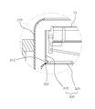
도 13은 본 발명에 따른 스핀식 헹굼 건조 장치로서, 기판감지부 및 세정부를 설명하기 위한 도면,
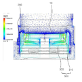
도 14는 본 발명에 따른 스핀식 헹굼 건조 장치에서, 기판거치부의 회전시의 기류 변화를 도시한 도면,
도 15는 본 발명에 따른 스핀식 헹굼 건조 장치에서, 기판거치부의 회전시의 압력 변화를 도시한 도면이다.
120 : 기판거치부 122 : 스핀 플레이트
124 : 가장자리 거치부 126 : 거치핀
200 : 가드링 210 : 상부 가드링
220 : 하부 가드링 230 : 유체배출유로
300 : 스핀커버 310 : 측면커버부
320 : 하부커버부 312 : 배출홀
400 : 기판감지부 400' : 세정부
Claims (27)
- 스핀식 헹굼 건조 장치로서,
상부에 기판이 안착되며, 회전 가능하게 마련되는 기판거치부와;
상기 기판거치부의 측면 둘레에 배치되는 가드링과;
상기 기판거치부의 주변을 감싸도록 형성되며, 상기 가드링의 내부에 배치되는 스핀커버를;
포함하는 것을 특징으로 하는 스핀식 헹굼 건조 장치.
- 제1항에 있어서,
상기 스핀커버는 상기 기판거치부가 회전함에 따라 발생되는 회전 기류를 감싸도록 마련된 것을 특징으로 하는 스핀식 헹굼 건조 장치.
- 제1항에 있어서,
상기 스핀커버는,
상기 기판거치부의 측면 둘레에 배치되는 측면커버부와;
상기 측면커버부의 하단에 연결되며 상기 기판거치부의 하부에 배치되는 하부커버부를;
포함하는 것을 특징으로 하는 스핀식 헹굼 건조 장치.
- 제3항에 있어서,
상기 스핀커버는 선택적으로 승강 가능하게 마련된 것을 특징으로 하는 스핀식 헹굼 건조 장치.
- 제3항에 있어서,
상기 스핀커버에는 상기 스핀커버의 내부에 유입된 유체를 상기 스핀커버의 외부로 배출하기 위한 배출홀이 형성된 것을 특징으로 하는 스핀식 헹굼 건조 장치.
- 제5항에 있어서,
상기 스핀커버는 회전 가능하게 마련된 것을 특징으로 하는 스핀식 헹굼 건조 장치.
- 제5항에 있어서,
상기 배출홀은 상기 하부커버부의 상면에 인접한 상기 측면커버부의 최하단에 형성된 것을 특징으로 하는 스핀식 헹굼 건조 장치.
- 제5항에 있어서,
상기 배출홀은 상기 스핀커버의 원주 방향을 따라 이격되게 복수개가 형성된 것을 특징으로 하는 스핀식 헹굼 건조 장치.
- 제5항에 있어서,
상기 배출홀은 원형홀 형태로 형성된 것을 특징으로 하는 스핀식 헹굼 건조 장치.
- 제5항에 있어서,
상기 배출홀은 폭보다 긴 길이를 갖는 장공홀 형태로 형성된 것을 특징으로 하는 스핀식 헹굼 건조 장치.
- 제3항에 있어서,
상기 하부커버부에는 상기 스핀커버의 내부에 유입된 유체를 상기 하부커버부의 중심에서 상기 하부커버부의 외측 방향으로 안내하는 경사안내부가 형성된 것을 특징으로 하는 스핀식 헹굼 건조 장치.
- 제11항에 있어서,
상기 경사안내부는 상기 하부커버부의 가장자리를 따라 형성된 것을 특징으로 하는 스핀식 헹굼 건조 장치.
- 제1항 내지 제12항 중 어느 한 항에 있어서,
상기 기판거치부의 하부에서 기체를 배기시키는 배기포트를 포함하는 것을 특징으로 하는 스핀식 헹굼 건조 장치.
- 제13항에 있어서,
상기 배기포트는 상기 스핀커버의 외면과 상기 가드링의 내면 사이의 공간과 연통되게 형성된 것을 특징으로 하는 스핀식 헹굼 건조 장치.
- 제14항에 있어서,
상기 가드링에는 상기 가드링의 내부에 유입된 유체를 상기 가드링의 외측으로 배출하는 유체배출유로가 형성된 것을 특징으로 하는 스핀식 헹굼 건조 장치.
- 제15항에 있어서,
상기 가드링은,
상기 스핀커버의 측면 둘레에 이격되게 배치되는 상부 가드링과;
상기 상부 가드링의 하부에 배치되는 하부 가드링을;
포함하는 것을 특징으로 하는 스핀식 헹굼 건조 장치.
- 제16항에 있어서,
상기 유체배출유로는 상기 상부 가드링과 상기 하부 가드링의 사이에 형성된 것을 특징으로 하는 스핀식 헹굼 건조 장치.
- 제17항에 있어서,
상기 하부 가드링은 상기 상부 가드링의 내경보다 작은 외경을 갖도록 형성되어 상기 상부 가드링의 하단에 중첩되게 배치되고,
상기 유체배출유로는 상기 상부 가드링의 내면과 상기 하부 가드링의 내면 사이에 마련되는 공간에 형성되는 것을 특징으로 하는 스핀식 헹굼 건조 장치.
- 제18항에 있어서,
상기 유체배출유로는 상기 가드링의 원주 방향을 따라 링 형태로 형성된 것을 특징으로 하는 스핀식 헹굼 건조 장치.
- 제17항에 있어서,
상기 상부 가드링은 회전 가능하게 마련된 것을 특징으로 하는 스핀식 헹굼 건조 장치.
- 제20항에 있어서,
상기 상부 가드링은 상기 기판과 동일한 방향으로 회전하는 것을 특징으로 하는 스핀식 헹굼 건조 장치.
- 제16항에 있어서,
상기 상부 가드링은 절곡된 단면 형태를 갖도록 형성된 것을 특징으로 하는 스핀식 헹굼 건조 장치.
- 제15항에 있어서,
상기 가드링의 외측에 배치되며 상기 유체를 드레인하는 드레인포트를 포함하는 것을 특징으로 하는 스핀식 헹굼 건조 장치.
- 제23항에 있어서,
상기 기판거치부의 회전시 상기 배기포트의 입구에는 음압이 형성되고, 상기 드레인포트의 입구에는 양압이 형성되는 것을 특징으로 하는 스핀식 헹굼 건조 장치.
- 제1항 내지 제12항 중 어느 한 항에 있어서,
상기 스핀커버에 장착되며 상기 기판을 감지하는 기판감지부를 더 포함하는 것을 특징으로 하는 스핀식 헹굼 건조 장치.
- 제1항 내지 제12항 중 어느 한 항에 있어서,
상기 스핀커버에 장착되며 상기 기판의 저면을 세정하는 세정부를 더 포함하는 것을 특징으로 하는 스핀식 헹굼 건조 장치.
- 제1항 내지 제12항 중 어느 한 항에 있어서,
상기 기판거치부는,
상기 가드링의 내부에 회전 가능하게 배치되는 스핀 플레이트와;
상기 스핀 플레이트의 상면에 구비되며 상기 기판을 지지하는 기판지지부와;
상기 스핀 플레이트의 가장자리 외측으로 돌출되게 배치되며, 상기 기판지지부와 상기 스핀 플레이트의 회전축을 연결하는 연결부를; 포함하고,
상기 스핀커버는 상기 연결부의 측면 둘레와 하부를 막도록 배치된 것을 특징으로 하는 스핀식 헹굼 건조 장치.
Priority Applications (2)
| Application Number | Priority Date | Filing Date | Title |
|---|---|---|---|
| KR1020170025894A KR101923382B1 (ko) | 2017-02-28 | 2017-02-28 | 스핀식 헹굼 건조 장치 |
| CN201721858170.9U CN207602532U (zh) | 2017-02-28 | 2017-12-27 | 旋转式漂洗干燥装置 |
Applications Claiming Priority (1)
| Application Number | Priority Date | Filing Date | Title |
|---|---|---|---|
| KR1020170025894A KR101923382B1 (ko) | 2017-02-28 | 2017-02-28 | 스핀식 헹굼 건조 장치 |
Publications (2)
| Publication Number | Publication Date |
|---|---|
| KR20180098997A true KR20180098997A (ko) | 2018-09-05 |
| KR101923382B1 KR101923382B1 (ko) | 2018-11-29 |
Family
ID=62769159
Family Applications (1)
| Application Number | Title | Priority Date | Filing Date |
|---|---|---|---|
| KR1020170025894A Active KR101923382B1 (ko) | 2017-02-28 | 2017-02-28 | 스핀식 헹굼 건조 장치 |
Country Status (2)
| Country | Link |
|---|---|
| KR (1) | KR101923382B1 (ko) |
| CN (1) | CN207602532U (ko) |
Families Citing this family (2)
| Publication number | Priority date | Publication date | Assignee | Title |
|---|---|---|---|---|
| CN115831821B (zh) * | 2022-12-12 | 2023-06-06 | 上海世禹精密设备股份有限公司 | 一种基板清洗干燥装置 |
| CN116078747A (zh) * | 2022-12-23 | 2023-05-09 | 苏州智安电子科技有限公司 | Ozec在线零污水排放超声波清洗一体机 |
Family Cites Families (3)
| Publication number | Priority date | Publication date | Assignee | Title |
|---|---|---|---|---|
| US5997653A (en) * | 1996-10-07 | 1999-12-07 | Tokyo Electron Limited | Method for washing and drying substrates |
| KR101087791B1 (ko) * | 2009-07-30 | 2011-11-30 | 주식회사 하이닉스반도체 | 스핀 척 및 이를 이용한 스핀 척 장치 |
| JP6220312B2 (ja) * | 2014-04-30 | 2017-10-25 | 東京エレクトロン株式会社 | 基板処理装置、基板処理装置の基板検知方法および記憶媒体 |
-
2017
- 2017-02-28 KR KR1020170025894A patent/KR101923382B1/ko active Active
- 2017-12-27 CN CN201721858170.9U patent/CN207602532U/zh active Active
Also Published As
| Publication number | Publication date |
|---|---|
| KR101923382B1 (ko) | 2018-11-29 |
| CN207602532U (zh) | 2018-07-10 |
Similar Documents
| Publication | Publication Date | Title |
|---|---|---|
| JP6051919B2 (ja) | 液処理装置 | |
| TWI529776B (zh) | 基板處理裝置 | |
| JP6022430B2 (ja) | 基板処理装置 | |
| JP4816747B2 (ja) | 液処理装置及び液処理方法 | |
| JP4538754B2 (ja) | 基板処理装置および基板処理方法 | |
| TWI538044B (zh) | 用來清洗基板處理裝置的清洗治具及清洗方法、與基板處理系統 | |
| JP7253029B2 (ja) | 基板処理装置 | |
| KR101042666B1 (ko) | 액 처리 장치 및 액 처리 방법 | |
| JP5387636B2 (ja) | 液処理装置 | |
| KR101923382B1 (ko) | 스핀식 헹굼 건조 장치 | |
| JP2008021983A (ja) | 液処理装置および液処理方法 | |
| JP4621038B2 (ja) | 半導体ウエハの洗浄方法及び半導体ウエハの洗浄装置 | |
| KR101677037B1 (ko) | 스핀식 헹굼 건조 장치 | |
| KR102493017B1 (ko) | 스핀식 헹굼 건조 장치 | |
| KR102781587B1 (ko) | 스핀식 헹굼 건조 장치 | |
| KR20180096917A (ko) | 스핀식 헹굼 건조 장치 | |
| JP4912020B2 (ja) | 液処理装置 | |
| KR102724389B1 (ko) | 기판 처리용 바울 및 이를 포함하는 기판처리장치 | |
| KR102924231B1 (ko) | 기판 세정 장치 | |
| KR102764058B1 (ko) | 기판 처리 장치 | |
| KR101318493B1 (ko) | 스핀 린스 드라이 장치 | |
| KR20170079268A (ko) | 스핀식 헹굼 건조 장치 | |
| KR100983759B1 (ko) | 기판의 매엽식 세정장치 | |
| CN120826766A (zh) | 基板处理装置 | |
| KR20190137217A (ko) | 기판 처리 장치 |
Legal Events
| Date | Code | Title | Description |
|---|---|---|---|
| A201 | Request for examination | ||
| PA0109 | Patent application |
St.27 status event code: A-0-1-A10-A12-nap-PA0109 |
|
| PA0201 | Request for examination |
St.27 status event code: A-1-2-D10-D11-exm-PA0201 |
|
| R18-X000 | Changes to party contact information recorded |
St.27 status event code: A-3-3-R10-R18-oth-X000 |
|
| PN2301 | Change of applicant |
St.27 status event code: A-3-3-R10-R13-asn-PN2301 St.27 status event code: A-3-3-R10-R11-asn-PN2301 |
|
| N231 | Notification of change of applicant | ||
| PN2301 | Change of applicant |
St.27 status event code: A-3-3-R10-R13-asn-PN2301 St.27 status event code: A-3-3-R10-R11-asn-PN2301 |
|
| D13-X000 | Search requested |
St.27 status event code: A-1-2-D10-D13-srh-X000 |
|
| D14-X000 | Search report completed |
St.27 status event code: A-1-2-D10-D14-srh-X000 |
|
| E902 | Notification of reason for refusal | ||
| PE0902 | Notice of grounds for rejection |
St.27 status event code: A-1-2-D10-D21-exm-PE0902 |
|
| E13-X000 | Pre-grant limitation requested |
St.27 status event code: A-2-3-E10-E13-lim-X000 |
|
| P11-X000 | Amendment of application requested |
St.27 status event code: A-2-2-P10-P11-nap-X000 |
|
| P13-X000 | Application amended |
St.27 status event code: A-2-2-P10-P13-nap-X000 |
|
| PG1501 | Laying open of application |
St.27 status event code: A-1-1-Q10-Q12-nap-PG1501 |
|
| E701 | Decision to grant or registration of patent right | ||
| PE0701 | Decision of registration |
St.27 status event code: A-1-2-D10-D22-exm-PE0701 |
|
| PR0701 | Registration of establishment |
St.27 status event code: A-2-4-F10-F11-exm-PR0701 |
|
| PR1002 | Payment of registration fee |
St.27 status event code: A-2-2-U10-U11-oth-PR1002 Fee payment year number: 1 |
|
| PG1601 | Publication of registration |
St.27 status event code: A-4-4-Q10-Q13-nap-PG1601 |
|
| PR1001 | Payment of annual fee |
St.27 status event code: A-4-4-U10-U11-oth-PR1001 Fee payment year number: 4 |
|
| R18-X000 | Changes to party contact information recorded |
St.27 status event code: A-5-5-R10-R18-oth-X000 |
|
| PR1001 | Payment of annual fee |
St.27 status event code: A-4-4-U10-U11-oth-PR1001 Fee payment year number: 5 |
|
| R18-X000 | Changes to party contact information recorded |
St.27 status event code: A-5-5-R10-R18-oth-X000 |
|
| PR1001 | Payment of annual fee |
St.27 status event code: A-4-4-U10-U11-oth-PR1001 Fee payment year number: 6 |
|
| PR1001 | Payment of annual fee |
St.27 status event code: A-4-4-U10-U11-oth-PR1001 Fee payment year number: 7 |
|
| PR1001 | Payment of annual fee |
St.27 status event code: A-4-4-U10-U11-oth-PR1001 Fee payment year number: 8 |
|
| U11 | Full renewal or maintenance fee paid |
Free format text: ST27 STATUS EVENT CODE: A-4-4-U10-U11-OTH-PR1001 (AS PROVIDED BY THE NATIONAL OFFICE) Year of fee payment: 8 |
|
| P22-X000 | Classification modified |
St.27 status event code: A-4-4-P10-P22-nap-X000 |