KR20180098492A - Solar cell and process of preparing the same - Google Patents
Solar cell and process of preparing the same Download PDFInfo
- Publication number
- KR20180098492A KR20180098492A KR1020180097398A KR20180097398A KR20180098492A KR 20180098492 A KR20180098492 A KR 20180098492A KR 1020180097398 A KR1020180097398 A KR 1020180097398A KR 20180097398 A KR20180097398 A KR 20180097398A KR 20180098492 A KR20180098492 A KR 20180098492A
- Authority
- KR
- South Korea
- Prior art keywords
- electrode layer
- region
- transparent
- layer
- light
- Prior art date
- Legal status (The legal status is an assumption and is not a legal conclusion. Google has not performed a legal analysis and makes no representation as to the accuracy of the status listed.)
- Ceased
Links
- 238000000034 method Methods 0.000 title claims description 25
- 230000008569 process Effects 0.000 title description 12
- 238000004519 manufacturing process Methods 0.000 claims abstract description 21
- 239000002131 composite material Substances 0.000 claims abstract description 3
- 239000000758 substrate Substances 0.000 claims description 29
- 230000000873 masking effect Effects 0.000 claims description 4
- OKTJSMMVPCPJKN-UHFFFAOYSA-N Carbon Chemical compound [C] OKTJSMMVPCPJKN-UHFFFAOYSA-N 0.000 claims description 2
- 229910052804 chromium Inorganic materials 0.000 claims description 2
- 238000001704 evaporation Methods 0.000 claims description 2
- 229910021389 graphene Inorganic materials 0.000 claims description 2
- 229910052748 manganese Inorganic materials 0.000 claims description 2
- 229910052750 molybdenum Inorganic materials 0.000 claims description 2
- 229910052758 niobium Inorganic materials 0.000 claims description 2
- 238000004544 sputter deposition Methods 0.000 claims description 2
- 229910052715 tantalum Inorganic materials 0.000 claims description 2
- 229910052719 titanium Inorganic materials 0.000 claims description 2
- 229910052721 tungsten Inorganic materials 0.000 claims description 2
- 229910052720 vanadium Inorganic materials 0.000 claims description 2
- 238000002834 transmittance Methods 0.000 abstract description 14
- 239000010409 thin film Substances 0.000 abstract description 10
- 230000005540 biological transmission Effects 0.000 abstract description 9
- 230000009467 reduction Effects 0.000 abstract description 4
- 239000010408 film Substances 0.000 abstract description 2
- 230000000052 comparative effect Effects 0.000 description 8
- 239000011521 glass Substances 0.000 description 8
- 238000010248 power generation Methods 0.000 description 6
- 238000005516 engineering process Methods 0.000 description 4
- 230000005611 electricity Effects 0.000 description 3
- 230000031700 light absorption Effects 0.000 description 3
- 230000035699 permeability Effects 0.000 description 3
- 229910021417 amorphous silicon Inorganic materials 0.000 description 2
- 238000000151 deposition Methods 0.000 description 2
- 239000000463 material Substances 0.000 description 2
- 230000000149 penetrating effect Effects 0.000 description 2
- 229910004613 CdTe Inorganic materials 0.000 description 1
- GYHNNYVSQQEPJS-UHFFFAOYSA-N Gallium Chemical compound [Ga] GYHNNYVSQQEPJS-UHFFFAOYSA-N 0.000 description 1
- 230000010748 Photoabsorption Effects 0.000 description 1
- PKLGPLDEALFDSB-UHFFFAOYSA-N [SeH-]=[Se].[In+3].[Cu+2].[SeH-]=[Se].[SeH-]=[Se].[SeH-]=[Se].[SeH-]=[Se] Chemical compound [SeH-]=[Se].[In+3].[Cu+2].[SeH-]=[Se].[SeH-]=[Se].[SeH-]=[Se].[SeH-]=[Se] PKLGPLDEALFDSB-UHFFFAOYSA-N 0.000 description 1
- IQTMWNQRJYAGDL-UHFFFAOYSA-N [SeH2]=[Se] Chemical compound [SeH2]=[Se] IQTMWNQRJYAGDL-UHFFFAOYSA-N 0.000 description 1
- 238000010521 absorption reaction Methods 0.000 description 1
- 230000015556 catabolic process Effects 0.000 description 1
- 230000008859 change Effects 0.000 description 1
- 150000001875 compounds Chemical class 0.000 description 1
- HVMJUDPAXRRVQO-UHFFFAOYSA-N copper indium Chemical compound [Cu].[In] HVMJUDPAXRRVQO-UHFFFAOYSA-N 0.000 description 1
- 229910021419 crystalline silicon Inorganic materials 0.000 description 1
- 238000006731 degradation reaction Methods 0.000 description 1
- 230000008021 deposition Effects 0.000 description 1
- 238000010586 diagram Methods 0.000 description 1
- 229910003460 diamond Inorganic materials 0.000 description 1
- 239000010432 diamond Substances 0.000 description 1
- 230000000694 effects Effects 0.000 description 1
- 229910052733 gallium Inorganic materials 0.000 description 1
- 229910010272 inorganic material Inorganic materials 0.000 description 1
- 239000011147 inorganic material Substances 0.000 description 1
- 238000009434 installation Methods 0.000 description 1
- 230000007774 longterm Effects 0.000 description 1
- 229910052751 metal Inorganic materials 0.000 description 1
- 239000002184 metal Substances 0.000 description 1
- 238000012986 modification Methods 0.000 description 1
- 230000004048 modification Effects 0.000 description 1
- 239000011368 organic material Substances 0.000 description 1
- 238000000059 patterning Methods 0.000 description 1
- 238000013082 photovoltaic technology Methods 0.000 description 1
- 238000002360 preparation method Methods 0.000 description 1
- 239000004065 semiconductor Substances 0.000 description 1
- 239000005361 soda-lime glass Substances 0.000 description 1
- 238000013083 solar photovoltaic technology Methods 0.000 description 1
- 238000010792 warming Methods 0.000 description 1
Images


Classifications
-
- H—ELECTRICITY
- H10—SEMICONDUCTOR DEVICES; ELECTRIC SOLID-STATE DEVICES NOT OTHERWISE PROVIDED FOR
- H10F—INORGANIC SEMICONDUCTOR DEVICES SENSITIVE TO INFRARED RADIATION, LIGHT, ELECTROMAGNETIC RADIATION OF SHORTER WAVELENGTH OR CORPUSCULAR RADIATION
- H10F71/00—Manufacture or treatment of devices covered by this subclass
- H10F71/138—Manufacture of transparent electrodes, e.g. transparent conductive oxides [TCO] or indium tin oxide [ITO] electrodes
-
- H01L31/1884—
-
- H01L31/022425—
-
- H01L31/022466—
-
- H01L31/02366—
-
- H01L31/03923—
-
- H01L31/042—
-
- H01L31/0445—
-
- H—ELECTRICITY
- H10—SEMICONDUCTOR DEVICES; ELECTRIC SOLID-STATE DEVICES NOT OTHERWISE PROVIDED FOR
- H10F—INORGANIC SEMICONDUCTOR DEVICES SENSITIVE TO INFRARED RADIATION, LIGHT, ELECTROMAGNETIC RADIATION OF SHORTER WAVELENGTH OR CORPUSCULAR RADIATION
- H10F19/00—Integrated devices, or assemblies of multiple devices, comprising at least one photovoltaic cell covered by group H10F10/00, e.g. photovoltaic modules
- H10F19/30—Integrated devices, or assemblies of multiple devices, comprising at least one photovoltaic cell covered by group H10F10/00, e.g. photovoltaic modules comprising thin-film photovoltaic cells
-
- H—ELECTRICITY
- H10—SEMICONDUCTOR DEVICES; ELECTRIC SOLID-STATE DEVICES NOT OTHERWISE PROVIDED FOR
- H10F—INORGANIC SEMICONDUCTOR DEVICES SENSITIVE TO INFRARED RADIATION, LIGHT, ELECTROMAGNETIC RADIATION OF SHORTER WAVELENGTH OR CORPUSCULAR RADIATION
- H10F77/00—Constructional details of devices covered by this subclass
- H10F77/10—Semiconductor bodies
- H10F77/16—Material structures, e.g. crystalline structures, film structures or crystal plane orientations
- H10F77/169—Thin semiconductor films on metallic or insulating substrates
- H10F77/1694—Thin semiconductor films on metallic or insulating substrates the films including Group I-III-VI materials, e.g. CIS or CIGS
-
- H—ELECTRICITY
- H10—SEMICONDUCTOR DEVICES; ELECTRIC SOLID-STATE DEVICES NOT OTHERWISE PROVIDED FOR
- H10F—INORGANIC SEMICONDUCTOR DEVICES SENSITIVE TO INFRARED RADIATION, LIGHT, ELECTROMAGNETIC RADIATION OF SHORTER WAVELENGTH OR CORPUSCULAR RADIATION
- H10F77/00—Constructional details of devices covered by this subclass
- H10F77/20—Electrodes
- H10F77/206—Electrodes for devices having potential barriers
- H10F77/211—Electrodes for devices having potential barriers for photovoltaic cells
-
- H—ELECTRICITY
- H10—SEMICONDUCTOR DEVICES; ELECTRIC SOLID-STATE DEVICES NOT OTHERWISE PROVIDED FOR
- H10F—INORGANIC SEMICONDUCTOR DEVICES SENSITIVE TO INFRARED RADIATION, LIGHT, ELECTROMAGNETIC RADIATION OF SHORTER WAVELENGTH OR CORPUSCULAR RADIATION
- H10F77/00—Constructional details of devices covered by this subclass
- H10F77/20—Electrodes
- H10F77/244—Electrodes made of transparent conductive layers, e.g. transparent conductive oxide [TCO] layers
-
- H—ELECTRICITY
- H10—SEMICONDUCTOR DEVICES; ELECTRIC SOLID-STATE DEVICES NOT OTHERWISE PROVIDED FOR
- H10F—INORGANIC SEMICONDUCTOR DEVICES SENSITIVE TO INFRARED RADIATION, LIGHT, ELECTROMAGNETIC RADIATION OF SHORTER WAVELENGTH OR CORPUSCULAR RADIATION
- H10F77/00—Constructional details of devices covered by this subclass
- H10F77/70—Surface textures, e.g. pyramid structures
- H10F77/707—Surface textures, e.g. pyramid structures of the substrates or of layers on substrates, e.g. textured ITO layer on a glass substrate
-
- Y—GENERAL TAGGING OF NEW TECHNOLOGICAL DEVELOPMENTS; GENERAL TAGGING OF CROSS-SECTIONAL TECHNOLOGIES SPANNING OVER SEVERAL SECTIONS OF THE IPC; TECHNICAL SUBJECTS COVERED BY FORMER USPC CROSS-REFERENCE ART COLLECTIONS [XRACs] AND DIGESTS
- Y02—TECHNOLOGIES OR APPLICATIONS FOR MITIGATION OR ADAPTATION AGAINST CLIMATE CHANGE
- Y02E—REDUCTION OF GREENHOUSE GAS [GHG] EMISSIONS, RELATED TO ENERGY GENERATION, TRANSMISSION OR DISTRIBUTION
- Y02E10/00—Energy generation through renewable energy sources
- Y02E10/50—Photovoltaic [PV] energy
- Y02E10/541—CuInSe2 material PV cells
-
- Y—GENERAL TAGGING OF NEW TECHNOLOGICAL DEVELOPMENTS; GENERAL TAGGING OF CROSS-SECTIONAL TECHNOLOGIES SPANNING OVER SEVERAL SECTIONS OF THE IPC; TECHNICAL SUBJECTS COVERED BY FORMER USPC CROSS-REFERENCE ART COLLECTIONS [XRACs] AND DIGESTS
- Y02—TECHNOLOGIES OR APPLICATIONS FOR MITIGATION OR ADAPTATION AGAINST CLIMATE CHANGE
- Y02P—CLIMATE CHANGE MITIGATION TECHNOLOGIES IN THE PRODUCTION OR PROCESSING OF GOODS
- Y02P70/00—Climate change mitigation technologies in the production process for final industrial or consumer products
- Y02P70/50—Manufacturing or production processes characterised by the final manufactured product
Landscapes
- Life Sciences & Earth Sciences (AREA)
- Engineering & Computer Science (AREA)
- Sustainable Development (AREA)
- Sustainable Energy (AREA)
- Photovoltaic Devices (AREA)
Abstract
본 발명은 태양전지 및 그 제조방법에 관한 것이다. 본 발명의 여러 구현예에 따르면, 투명전도성 전극 상에 제조된 CIGS 박막 태양전지 내에서 태양광 모듈 제작 중에 필수적으로 형성되는 스크라이빙 영역(면적 중 일부가 광 투과 가능한 PV)을 통해 광투과성을 확보할 수 있다. 또한, 모듈의 디자인(P1, P2, P3, 스크라이빙의 폭과 간격 등)에 따라 광투과성의 정도는 조절 가능하고, 스크라이빙으로 인한 10% 정도의 빈 공간을 통해 충분한 광 투과가 가능하다. 또한, 투명전도성 전극 상에 고전도성 불투명 전극을 마스크를 사용하여 증착시켜 복합 후면전도층막을 제조함으로써 투명전도성 후면전극만을 이용할 경우 야기되는 태양전지 효율 감소를 최소화할 수 있다. The present invention relates to a solar cell and a manufacturing method thereof. According to various embodiments of the present invention, the light transmission through the scribing region (a part of which is optically transparent) formed in a CIGS thin film solar cell fabricated on a transparent conductive electrode, . In addition, the degree of light transmittance can be adjusted according to the design of the module (P1, P2, P3, the width and spacing of the scribing, etc.), and sufficient light transmission is possible through 10% empty space due to scribing . In addition, a high conductivity non-transparent electrode is deposited on the transparent conductive electrode using a mask to produce a composite rear conductive layer film, thereby minimizing the reduction in the efficiency of the solar cell caused by using only the transparent conductive rear electrode.
Description
본 발명은 태양전지(PV) 및 그 제조방법에 관한 것이다. 더욱 구체적으로 CIGS 박막 태양전지 내에서 태양광 모듈 제작 중에 필수적으로 형성되는 스크라이빙 영역(면적 중 일부가 광 투과 가능한 PV)을 통해 효율 감소는 최소화하면서 광투과성을 확보할 수 있는 태양전지 및 그 제조방법에 관한 것이다. The present invention relates to a solar cell (PV) and a manufacturing method thereof. More specifically, in a CIGS thin film solar cell, a photovoltaic cell capable of securing light transmission while minimizing the efficiency reduction through a scribing region (a part of which is optically transparent PV) And a manufacturing method thereof.
기후 변화, 특히 지구 온난화에 대한 우려 증가로 인하여 태양 에너지를 전기로 변환하는 기술은 최근에 점점 더 주목을 받고 있다. 태양광 시스템은 땅, 옥상 및 심지어 빌딩의 벽에도 설치되어 대규모 방식에 의하여 전기를 생산할 수 있다. 태양광 기술의 발달은 2015년에 전세계 용량을 기준으로 227 GW 이상을 생산할 수 있는 글로벌 태양광 시스템의 설치를 가속화하고 있고, 매년 약 25% 정도의 빠른 성장을 보이고 있다. Due to increased concern about climate change, especially global warming, the technology to convert solar energy into electricity has received increasing attention in recent years. Photovoltaic systems can also be installed on land, rooftops, and even walls of buildings to produce electricity on a large scale. The development of photovoltaic technology is accelerating the installation of global photovoltaic systems, which can produce more than 227 GW of capacity worldwide by 2015, and is growing by about 25% annually.
게다가 최근 태양광 시설을 통한 대규모 전기 생산에 대한 세계적 관심사가 각 나라의 급격한 도시화와 연계된 에너지 자원 활용, 즉 고분산화된 현장 전기 에너지 생산 시스템 개발 및 적용으로 변화하고 있다. 이러한 마이크로그리드라고도 불리는 지역적으로 분산된 전기 생산 시스템은 메인 그리드가 작동하지 않는 동안에 작동될 수 있으며 그로 인해 지역적인 전기 생산 시스템은 그리드 회복력을 강화할 수 있고, 그리드의 장애를 완화할 수 있다. 게다가, 지역의 필요에 부응하기 위한 지역 자원의 사용은 전송 및 공급에서의 에너지 손실을 줄이는데 도움이 되며, 이로 인해 전기전달 시스템의 효율을 더욱 증가시킨다. In addition, recent global interest in large-scale electricity production through photovoltaic facilities is changing to the utilization of energy resources associated with the rapid urbanization of each country, namely the development and application of high-volume oxidized field electric energy production systems. A locally distributed electrical production system, also referred to as a microgrid, can be operated while the main grid is not operating, which allows the local electrical production system to enhance grid resilience and mitigate grid failures. In addition, the use of local resources to meet local needs helps to reduce energy losses in transmission and supply, thereby further increasing the efficiency of the electrical delivery system.
마이크로그리드 전기 생산 시스템의 대표적인 예로 전력 생산을 동반하는, 건물 외피에서 태양전지를 작동하는 건물 일체형 태양광 발전(Building integrated photovoltaic, BIPV)을 들 수 있다. 현재 결정질 실리콘 태양전지 기술이 지배적인 건물 태양광 기술로 적용되고 있으나 이외에도 무정형 실리콘(a-Si), 구리 인듐 다이-셀레나이드(CIS), 구리 인듐 갈륨 다이-셀레나이드(CIGS), 카드뮴 텔레나이트(CdTe)과 같은 무기물 필름 형태의 태양광 물질과 몇몇 유기물질들(예를 들어, OPV) 또한 건물 일체형 태양광 발전에 일부 활용되고 있다. A typical example of a microgrid electric production system is building integrated photovoltaic (BIPV), which operates a solar cell in a building envelope, accompanied by power generation. Crystalline silicon solar cell technology is currently being applied as the dominant solar photovoltaic technology. However, amorphous silicon (a-Si), copper indium di-selenide (CIS), copper indium gallium di-selenide (CIGS) (CdTe), and some organic materials (eg, OPV) are also being utilized in building integrated photovoltaics.
하지만 많은 형태의 BIPV 태양전지 중에서, 동력 발전 창으로 사용될 수 있는 태양전지는 매우 제한적이며, 가장 큰 원인으로는 창호용 태양전지가 만족해야 하는 서로 상반되는 기능, 즉 고전력 생산을 위한 빛 흡수 기능과 투광성 확보를 위한 가시역광선에 대한 투과 기능을 동시에 만족해야 하기 때문이라고 할 수 있다. 또 다른 중요 요구 조건은 심미적인 부분, 즉 태양전지 창의 멋진 외관(예를 들어, 색상)의 필요성을 들 수 있다. However, among the many types of BIPV solar cells, solar cells that can be used as power generation windows are very limited, and the biggest cause is the opposite function, that is, the light absorbing function for high power production And the transmission function for the visible backlight for securing the light transmittance must be satisfied at the same time. Another important requirement is the aesthetic part: the need for a beautiful appearance (eg, color) of the solar cell window.
현재까지 개발된 다양한 태양전지 중 염료감응형 태양전지는 창호형 태양전지가 갖추어야 하는 몇 가지 핵심 조건 (예를 들어, 반투명성, 다채로움, 낮은 비용 등)을 만족하여 그동안 창호용 태양전지의 유망한 후보로 고려되어 왔으나 아직까지는 저내구성 및 불안정성과 같은 심각한 단점을 아직까지 극복하지 못해 실제 적용을 하지 못하고 있는 실정이다. 그러므로, 현재까지는 창호용 태양전지로 응용할 수 있는 태양전지 대안이 부재한 상태이며 따라서 어느 정도의 광투과성을 확보할 수 있으며 고효율, 고내구성을 갖고 있어 동력 발전 창 어플리케이션에 대한 좋은 대안이 될 수 있는 태양전지의 개발이 필요하다. Among the various solar cells developed to date, the dye-sensitized solar cell satisfies some core conditions (for example, translucency, versatility, low cost, etc.) required for a window-type solar cell, However, it has not yet been able to overcome serious shortcomings such as low durability and instability. Therefore, until now, there is no solar cell alternative that can be applied to window solar cells, and thus it is possible to secure a certain degree of light transmittance, and has high efficiency and high durability, which is a good alternative to power generation window application The development of solar cells is necessary.
무기물 소재 기반의 박막 태양전지는 충분한 내구성 및 고효율이 이미 입증되어 왔다. 특히, 광흡수층으로 CIGS 필름을 포함하는 화합물 박막 태양전지는 높은 광에너지 효율, 장기 안정성 등과 같은 다양한 이점을 가지기 때문에 가장 유망한 박막 태양전지로 고려되어 왔다. 더욱 중요하게는, 이들은 투명전도성 유리 기판 상에 제작이 가능하기 때문에 창호용 태양전지의 중요 요소인 광투과성 확보가 가능하여 차세대 동력 발전 창으로 응용될 수 있다. Thin film solar cells based on inorganic materials have been proven to have sufficient durability and high efficiency. In particular, a compound thin film solar cell including a CIGS film as a light absorbing layer has been considered as the most promising thin film solar cell because it has various advantages such as high light energy efficiency and long term stability. More importantly, since they can be formed on a transparent conductive glass substrate, it is possible to secure light transmittance, which is an important factor of a solar cell for a window, and can be applied as a next generation power generation window.
CIGS 박막 태양전지의 광투과능을 부여하기 위해 두 가지 방법이 사용된다. 전 면적에 걸쳐 반투명한 전지를 사용하거나 또는 면적 중 일부가 광 투과 가능한 전지를 사용하는 것이 그것이다. 그러나, 상술한 바와 같이, 광투과성 및 태양전지 성능은 상반되는 기능이어서 반투과 박막 태양전지는 높은 태양전지 효율은 기대하기 어렵다. 따라서 CIGS 태양전지의 모듈 제작 시 수반되는 스크라이빙 영역을 조절함으로써 투광성을 확보하는 접근이 더 효과적이라고 할 수 있다. 또한 투명전도성 유리 기판 사용으로 인해 야기되는 효율 저하 문제를 해결할 수 있는 기술 개발이 필요하다. Two methods are used to impart the light transmittance of CIGS thin film solar cells. A semi-transparent cell is used over the entire area, or a cell that is partially light-transmissive is used. However, as described above, since the light transmittance and solar cell performance are opposite to each other, it is difficult to expect a high solar cell efficiency in a semi-transmissive thin film solar cell. Therefore, it is more effective to secure transparency by controlling the scribing area involved in the fabrication of CIGS solar cell modules. Also, it is necessary to develop a technology that can solve the problem of efficiency decrease caused by using transparent conductive glass substrate.
본 발명에서는 CIGS 박막 태양전지 내에서 태양광 모듈 제작 중에 필수적으로 형성되는 스크라이빙 영역(면적 중 일부가 광 투과 가능한 PV)을 통한 광투과성을 확보할 수 있는 발명을 제공하고자 한다. 모듈의 디자인(P1, P2, P3, 스크라이빙의 폭과 간격 등)에 따라, 광투과성의 정도는 조절 가능하고, 스크라이빙으로 인한 10% 정도의 빈 공간을 통해 충분한 광 투과가 가능할 뿐만 아니라 창밖을 볼 수 있도록 하며 동시에 불투명한 유리 기판 전극 (예: Mo-glass)를 사용할 때 비해 투명한 유리 기판 전극 (예: ITO-glass)를 사용할 때 생기는 효율 저하를 최소화 할 수 있는 발명을 제공하고자 한다. The present invention provides an invention capable of securing light transmittance through a scribing region (a part of the area is light-transmittable PV) which is essentially formed in a CIGS thin film solar cell during the manufacture of a solar module. Depending on the design of the module (P1, P2, P3, the width and spacing of the scribing, etc.), the degree of light transmission is adjustable and not only is sufficient light transmission possible through a 10% empty space due to scribing And to provide an invention that can minimize the efficiency degradation when using transparent glass substrate electrodes (e.g., ITO-glass) compared to opaque glass substrate electrodes (e.g., Mo-glass) .
본 발명의 대표적인 일 측면은 이러한 과제 달성을 위한 태양전지 제조방법 및 그렇게 제조된 태양전지에 관한 것이다. A representative aspect of the present invention relates to a method of manufacturing a solar cell and a solar cell so constructed.
본 발명의 여러 구현예에 따르면, CIGS 박막 태양전지 내에서 태양광 모듈 제작 중에 필수적으로 형성되는 스크라이빙 영역(면적 중 일부가 광 투과 가능한 PV)을 통해 광투과성을 확보할 수 있다. 또한, 모듈의 디자인(P1, P2, P3, 스크라이빙의 폭과 간격 등)에 따라 광투과성의 정도는 조절 가능하고, 스크라이빙으로 인한 10% 정도의 빈 공간을 통해 충분한 광 투과가 가능하다. 또한, 마스크를 이용 P3 스크라이빙 영역을 제외한 부분에 Mo와 같은 전도성이 높은 금속을 증착, CIGS 광흡수층과 후면전극 사이의 Ohmic 접합을 가능하게 하여 투명한 유리 기판 전극을 사용할 때 생기는 효율 저하를 최소화 할 수 있다. According to various embodiments of the present invention, light transmittance can be ensured through a scribing region (a part of which is optically transparent) formed in a CIGS thin film solar cell, which is indispensably formed during the production of a solar module. In addition, the degree of light transmittance can be adjusted according to the design of the module (P1, P2, P3, the width and spacing of the scribing, etc.), and sufficient light transmission is possible through 10% empty space due to scribing . In addition, by using a mask, a highly conductive metal such as Mo is deposited on the portion excluding the P3 scribing region, and Ohmic bonding is performed between the CIGS light absorption layer and the rear electrode, thereby minimizing a reduction in efficiency caused by using a transparent glass substrate electrode can do.
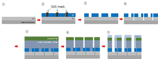
도 1은 본 발명의 실시예에 따른 ITO와 Mo를 동시 이용한 투광형 CIGS 단일형(monolithic) 모듈의 제조 순서 및 각 층별 물질 과 구조를 나타낸 도면이다.
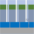
도 2는 일반적인 CIGS 단일형(monolithic) 모듈의 제조 완료된 단면 구조와 스크라이빙 영역을 나타낸 도면이다.
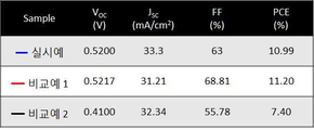
도 3은 본 발명의 실시예 (ITO와 Mo를 동시 이용) 와 기존의 비교예 1 (Mo 이용), 2 (ITO 이용) 의 기판별 효율 비교를 나타내기 위한 싱글 셀의 대한 효율 그래프(3a) 와 표(3b) 이다.
도 4는 본 발명의 실시예 (ITO와 Mo를 동시 이용) 와 기존의 비교예 1(Mo 이용), 2 (ITO 이용) 모듈의 제조 완료된 투과도 비교를 나타낸 사진이다.FIG. 1 is a view showing a manufacturing procedure of a light-emitting type CIGS monolithic module using both ITO and Mo according to an embodiment of the present invention, and materials and structures of respective layers.
FIG. 2 is a diagram showing a manufactured cross-sectional structure and a scribing area of a general CIGS monolithic module. FIG.
FIG. 3 is a graph showing the efficiency versus efficiency (3a) for a single cell to show the efficiency comparison between the embodiments of the present invention (using ITO and Mo simultaneously) and the conventional comparative examples 1 (using Mo) and 2 (using ITO) And Table (3b).
FIG. 4 is a photograph showing comparison of manufactured transmittance of the embodiment of the present invention (using ITO and Mo at the same time) and the conventional comparative examples 1 (using Mo) and 2 (using ITO).
이하에서, 본 발명의 여러 측면 및 다양한 구현예에 대해 더욱 구체적으로 살펴보도록 한다. Hereinafter, various aspects and various embodiments of the present invention will be described in more detail.
본 발명의 일 측면에 따르면, (A) 투명성 절연 기판 위에 투명성 하부 전극층을 형성하는 단계, (B) 상기 투명성 하부 전극층이 형성되어 있는 전체 영역인 셀 영역 중 일부인 투광 영역을 제외한 나머지 영역인 비투광 영역에 고전도성 하부 전극층(비투명전극층)을 형성시켜 복합 하부 전극층을 수득하는 단계, (C) 상기 비투광 영역 중에서 그 일부 영역인 단락 영역에 대해서만 그 수직 하방향으로 존재하는 비투명성 하부 전극층 및 투명성 하부 전극층을 제거하고 (P1 스크라이빙), 그 나머지 영역인 비단락 영역은 그대로 둠으로써, 서로 단락된 복수 개의 복합 하부 전극층을 수득하는 단계, (D) 상기 (C) 단계를 거친 후 그 상부에 광흡수층, 버퍼층, 윈도우층을 형성시키는 단계, (E) 상기 비투광성 영역 중 일부 영역인 도전성 영역의 수직 상하방향에 존재하는 상기 광흡수층, 상기 버퍼층, 상기 윈도우층을 제거하는 단계 (P2 스크라이빙), (F) 상기 (E) 단계를 거친 후 그 상부에 상부 전극층을 형성하는 단계, (G) 상기 투광성 영역에 대해서 그 수직 상하방향에 존재하는 상기 광흡수층, 상기 버퍼층, 상기 윈도우층, 및 상기 상부 전극층을 제거하는 단계 (P3 스크라이빙)를 포함하는 태양전지 제조방법에 관한 것이다. According to an aspect of the present invention, there is provided a method of manufacturing a semiconductor device, comprising: (A) forming a transparent lower electrode layer on a transparent insulating substrate; (B) (C) a non-transparent lower electrode layer existing in a vertically downward direction only with respect to a short-circuit region which is a partial region of the non-transparent region, and (D) a step of removing the transparent lower electrode layer (P1 scribing) and leaving the remaining short-circuiting area as it is, thereby obtaining a plurality of composite lower electrode layers short-circuited to each other; Forming a light absorption layer, a buffer layer, and a window layer on the upper portion of the non-light-transmitting region, (E) (E), forming an upper electrode layer on the light absorbing layer, the buffer layer, and the window layer (P2 scribing); (G) And removing the light absorbing layer, the buffer layer, the window layer, and the upper electrode layer existing in the vertical vertical direction (P3 scribing).
위 (B) 단계를 거쳐, 투명성 하부 전극층의 최초 전체 영역인 셀 영역은 비투명성 하부 전극층이 그 위에 형성되어 있는 영역인 비투광 영역과 그 나머지 영역인 투광 영역으로 나눌 수 있다. Through the above step (B), the cell region, which is the first entire region of the transparent lower electrode layer, can be divided into a non-transparent region, which is a region where the non-transparent lower electrode layer is formed, and a transparent region, which is the remaining region.
또한 위 (C) 단계에 의해, 최초 비투광 영역은 현재 단계에서 비투명성 하부 전극층과 투명성 하부 전극층이 모두 제거된 영역은 단락 영역과 그 나머지 영역은 비단락 영역으로 나눌 수 있다. In the step (C), the region where the non-transparent lower electrode layer and the transparent lower electrode layer are both removed at the current stage may be divided into the short-circuited region and the remaining region as the non-short-circuited region.
또한, 위 (D) 단계를 통해서, 단락 영역에는 투명성 절연 기판 위에, 투광 영역에는 투명성 하부 전극층 위에, 비투광성 영역에는 비투명성 하부 전극층 위에 광흡수층, 버퍼층, 윈도우층이 형성되게 된다. 즉, 투명성 절연 기판에서 복합 하부 전극층이 제거되어 투명성 절연 기판이 드러난 영역에는 투명성 절연 기판 위에 위 3개 층을 형성되고, 또한 복합 하부 전극층 위에 위 3개 층을 형성시키는 경우에도 비투명성 하부 전극층이 형성된 영역에는 비투명성 하부 전극층 위에 위 3개 층을 형성시키고, 비투명성 하부 전극층이 형성되지 않은 영역에는 투명성 하부 전극층 위에 위 3개 층을 형성시킨다는 의미이다. Through the step (D), a light absorbing layer, a buffer layer, and a window layer are formed on the transparent insulating substrate in the short-circuit region, on the transparent lower electrode layer in the light transmitting region, and on the non-transparent lower electrode layer in the non-transmissive region. That is, even when the upper three layers are formed on the transparent insulating substrate and the upper three layers are formed on the complex lower electrode layer in the region where the transparent lower insulating layer is removed from the transparent insulating substrate, the non-transparent lower electrode layer It means that the upper three layers are formed on the non-transparent lower electrode layer and the upper three layers are formed on the transparent lower electrode layer in the region where the non-transparent lower electrode layer is not formed.
위 (E) 단계는 하기 본 발명의 일 구현예에 따른 공정도 중 ⑥번 공정에 해당되는 단계이다. Step (E) corresponds to step (6) of the process according to an embodiment of the present invention.
또한, 위 (F) 단계를 통해서, 도전성 영역에는 비투광성 하부 전극층 위에, 그 나머지 셀 영역에는 윈도우층 위에 상부 전극층이 형성되게 된다. 즉, 상기 비투명성 하부 전극층의 수직 상방향으로 존재하는 광흡수층, 버퍼층, 윈도우층이 제거된 영역은 제거되면서 드러난 비투명성 하부 전극층 위에 상부 전극층이 형성되며, 제거되지 않은 영역은 맨 위의 윈도우층 위에 상부 전극층이 형성된다. Further, through the above step (F), the upper electrode layer is formed on the non-conductive lower electrode layer in the conductive region and on the window layer in the remaining cell region. That is, the upper electrode layer is formed on the non-transparent lower electrode layer exposed by removing the light absorbing layer, the buffer layer, and the window layer removed in the vertical direction of the non-transparent lower electrode layer, and the non- An upper electrode layer is formed.
위 (G) 단계에서, 투광성 영역에는 (B) 단계를 통하여 비투광성 하부 전극층은 존재하지 않으므로 그 수직 상하방향으로 존재하는 광흡수층, 버퍼층, 윈도우층의 3개 층과 상부 전극층을 제거하면 된다. In step (G), since the non-transparent lower electrode layer does not exist through the step (B) in the light transmitting region, the three layers of the light absorbing layer, the buffer layer and the window layer and the upper electrode layer existing in the vertical vertical direction can be removed.
이와 같은 본 발명의 일 구현예에 있어서, 상기 (B) 단계는 상기 투광 영역에 대해 마스킹한 후 상기 고전도성 비투명 하부 전극층을 형성하고 상기 마스킹을 제거함으로써 수행된다. In one embodiment of the present invention, the step (B) is performed by masking the light-transmitting region and then forming the highly conductive non-transparent lower electrode layer and removing the masking.
다른 구현예에 있어서, 상기 고전도성 비투과 전극층은 E-빔 증발법 또는 스퍼터링법에 의해 형성된다. In another embodiment, the highly conductive non-penetrating electrode layer is formed by an E-beam evaporation method or a sputtering method.
또 다른 구현예에 있어서, 상기 투과성 전극층은 ITO, FTO, AZO, graphene 중에서 선택된 1종 이상이다. In another embodiment, the transmissive electrode layer is at least one selected from the group consisting of ITO, FTO, AZO, and graphene.
또 다른 구현예에 있어서, 상기 고전도성 비투과 전극층은 Mo, W, Cr, Ta, Nb, V, Ti, Mn 중에서 선택된 1종 이상이다. In another embodiment, the highly conductive non-penetrating electrode layer is at least one selected from the group consisting of Mo, W, Cr, Ta, Nb, V, Ti and Mn.
또 다른 구현예에 있어서, 상기 (C) 단계는 레이저 스크라이빙법에 의해 수행된다. In another embodiment, the step (C) is performed by a laser scribing method.
또 다른 구현예에 있어서, 상기 (E) 단계는 메커니컬 스크라이빙법에 의해 수행된다. In another embodiment, the step (E) is performed by a mechanical scribing method.
또 다른 구현예에 있어서, 상기 (G) 단계는 메커니컬 스크라이빙법에 의해 수행된다. In another embodiment, step (G) is performed by a mechanical scribing method.
본 발명의 다른 측면은 본 발명의 여러 구현예에 따라 제조된 태양전지에 관한 것이다.
Another aspect of the present invention relates to a solar cell manufactured according to various embodiments of the present invention.
이하에서 실시예 등을 통해 본 발명을 더욱 상세히 설명하고자 하며, 다만 이하에 실시예 등에 의해 본 발명의 범위와 내용이 축소되거나 제한되어 해석될 수 없다. 또한, 이하의 실시예를 포함한 본 발명의 개시 내용에 기초한다면, 구체적으로 실험 결과가 제시되지 않은 본 발명을 통상의 기술자가 용이하게 실시할 수 있음은 명백한 것이며, 이러한 변형 및 수정이 첨부된 특허청구범위에 속하는 것도 당연하다. Hereinafter, the present invention will be described in more detail with reference to Examples and the like, but the scope and content of the present invention can not be construed to be limited or limited by the following Examples. It will be apparent to those skilled in the art that various modifications and variations can be made in the present invention without departing from the spirit and scope of the present invention as set forth in the following claims. It is natural that it belongs to the claims.
또한 이하에서 제시되는 실험 결과는 상기 실시예 및 비교예의 대표적인 실험 결과만을 기재한 것이며, 아래에서 명시적으로 제시하지 않은 본 발명의 여러 구현예의 각각의 효과는 해당 부분에서 구체적으로 기재하도록 한다. In addition, the experimental results presented below only show representative experimental results of the embodiments and the comparative examples, and the respective effects of various embodiments of the present invention which are not explicitly described below will be specifically described in the corresponding part.
실시예 Example
실시예: ITO와 Mo를 동시 이용한 투광형 CIGS 단일형(monolithic) 모듈의 제조Example: Fabrication of light-emitting type CIGS monolithic module using ITO and Mo simultaneously
투광형 CIGS 단일형(monolithic) 모듈을 제작함에 있어 ITO 기판의 단일 사용은 ITO 기판의 상대적으로 높은 면 저항으로 인하여 비투광형(Mo 기판 이용)과 비교했을 때 효율이 낮다(도 3의 비교예 2). 때문에 ITO 기판의 투과성(도 4의 비교예 2)과 Mo 기판의 낮은 면 저항에 따른 높은 효율(도 3의 비교예 1)을 동시에 충족하기 위해 스테인레스 스틸(SS) 마스크를 사용하여 CIGS 단일형(monolithic) 모듈을 구현하였다. The single use of an ITO substrate in fabricating a light-emitting CIGS monolithic module is less efficient compared to a non-transmissive (Mo substrate) due to the relatively high surface resistance of the ITO substrate (Comparative Example 2 ). Therefore, in order to satisfy both the permeability of the ITO substrate (Comparative Example 2 in Fig. 4) and the high efficiency due to the low surface resistance of the Mo substrate (Comparative Example 1 in Fig. 3), a CIGS monolithic ) Module.
우선, ITO 기판에 SS 마스크를 모듈디자인에 맞게 제작하여 올린 후(도 1의 ①), Mo를 E-빔 증발기(E-beam evaporator) 또는 스퍼터를 사용하여 증착하였다(②, ③). 부분적으로 전도성이 없는 소다 라임 유리만 남겨두어 하부전극을 셀 단위로 단절(isolation)시키기 위해 532 레이저 장비를 이용하여 Mo와 ITO 기판의 해당 부분을 제거하였다(④, P1 공정). First, an SS mask was fabricated on the ITO substrate in accordance with the module design and then deposited (① in FIG. 1). Then, Mo was deposited using an E-beam evaporator or a sputterer (②, ③). In order to isolate the lower electrode cell by leaving only partly unconducting soda lime glass, the corresponding part of Mo and ITO substrate was removed by using 532 laser equipment (④, P1 process).
P1 공정 처리된 기판에 CIGS 광흡수층과 CdS 버퍼층 및 IZO 윈도우층을 증착하였다(⑤). 이후 P1에서 단절된 단위 셀들을 상부전극이 되는 AZO물질이 하부전극에 닿아 단위 셀들을 직렬로 연결하게 된다. 이를 위해 우선 IZO 층 증착 후 AZO를 증착하기 전 P2 공정을 폭 50 μm의 다이아몬드 니들을 사용하여 메커니컬 스크라이빙으로 진행하였다(⑥, P2 공정). 이러한 P2 공정을 통해서 위에 언급한 하부전극인 Mo 상단의 광 흡수층, 버퍼층, 윈도우층을 제거하였다. A CIGS photoabsorption layer, a CdS buffer layer, and an IZO window layer were deposited on the P1-processed substrate (⑤). Then, the unit cells disconnected at P1 are connected to the lower electrode by the AZO material, which is the upper electrode, to connect the unit cells in series. For this purpose, the P2 process was performed by mechanical scribing using diamond needles with a width of 50 μm (⑥, P2 process) before depositing AZO after IZO layer deposition. Through the P2 process, the upper absorption layer, the buffer layer, and the window layer on the lower electrode, Mo, were removed.
P2 공정 이후 상부전극인 AZO를 증착 및 메카니컬 스크라이빙을 통해 ②번 단계의 도면에서 마스킹되어 비투광형 하부전극인 Mo이 증착되지 않은 부분에 ITO 위 부분의 층들을 제거하였으며(⑦, P3 공정), 이를 통해 단위 셀끼리 직렬로 연결시켰다. P3 공정이 수행된 부분의 투과도와 부분적으로 증착된 낮은 저항의 하부전극 Mo를 이용한 투광형 CIGSSe 단일형(monolithic) 모듈이 얻어졌다.
After the P2 process, the upper electrode AZO was deposited and mechanically scribed to remove layers on the ITO upper portion of the non-transparent lower electrode, which was masked in the drawing of
도 4의 실시예의 결과를 보면 하부전극 ITO 기판을 통해 투광형을 가지는 것을 알 수 있고, 동시에 도 3의 그래프를 보면 ITO와 Mo 기판 모두를 이용한 단위 셀의 경우 Mo 기판만을 이용한 단위 셀과 비교해서도 비슷한 효율을 보임을 알 수 있다. The result of the embodiment of FIG. 4 shows that the lower electrode ITO substrate has a light transmission type. In the graph of FIG. 3, the unit cell using both ITO and Mo substrate is compared with the unit cell using only the Mo substrate Which is similar to that shown in Fig.
비교예 1: Mo를 이용한 CIGS 단일형(monolithic) 모듈의 제조Comparative Example 1: Preparation of CIGS monolithic module using Mo
CIGS 단일형(monolithic) 모듈을 제작하기 위해 하부전극으로 Mo 기판만을 사용하였다. 일반적으로 Mo 기판은 2 내지 5 Ω/cm2의 면저항을 가진다. 단일형(monolithic) 모듈 제작을 위해 532 레이저를 이용하여 도 2의 1 구조 형성을 위해 P1 공정을 진행하였다. P1 공정이 진행된 부분은 Mo이 제거되기 때문에 전도성이 없는 유리만 남아 셀 단위로 단락된다. 이후 위의 위 실시예와 동일하게 P3까지 공정을 진행하여 투과도는 가지지 않지만 일반적인 효율을 보여주는 Mo 기판의 CIGS 단일형(monolithic) 모듈을 제조하였다.To fabricate the CIGS monolithic module, only the Mo substrate was used as the lower electrode. In general, the Mo substrate has a sheet resistance of 2 to 5 Ω / cm 2 . For the fabrication of the monolithic module, the P1 process was performed to form the structure of FIG. 2 using the 532 laser. Since the Mo part is removed at the portion where the P1 process is performed, only the glass having no conductivity is left and the cell is short-circuited. Thereafter, the CIGS monolithic module of the Mo substrate was fabricated to show the general efficiency even though the process up to P3 was not carried out as in the above embodiment.
비교예 2: ITO를 이용한 투광형 CIGS 단일형(monolithic) 모듈의 제조Comparative Example 2: Fabrication of light emitting type CIGS monolithic module using ITO
CIGS 단일형(monolithic) 모듈에서의 도 2에서 3에 해당하는 스크라이빙 영역을 통한 투광성 향상을 이용하기 위하여 하부 전극으로 ITO 기판을 사용하였다. ITO 기판은 일반적으로 Mo 기판보다는 높은 8 내지 10 Ω/cm2 정도의 면저항을 갖는다. 위 실시예와 마찬가지로 패터닝 공정까지 동일하게 진행하였다. 완성된 단일형(monolithic) 모듈은 ITO의 투광성으로 인해 P3 부분은 투과도가 없는 Mo와는 다르게 상대적으로 높은 투과도를 가지며 목적에 따라 원하는 투과도를 위해 P3 폭을 늘려서 활용할 수 있다. 제조된 하부전극이 ITO 기판인 CIGS 단일형(monolithic) 모듈은 Mo 기판보다는 다소 높은 면저항으로 인해 투과도는 가지지만 효율은 상대적으로 낮음을 확인할 수 있다.An ITO substrate was used as the lower electrode to utilize the translucency enhancement through the scribing area corresponding to FIGS. 2 to 3 in the CIGS monolithic module. The ITO substrate generally has a sheet resistance of about 8 to 10 OMEGA / cm < 2 > higher than that of the Mo substrate. As in the case of the above embodiment, the patterning process was the same. The completed monolithic module has a higher transmittance than the Mo having no transmittance due to the light transmittance of the ITO, and can be utilized by increasing the P3 width for the desired transmittance according to the purpose. The CIGS monolithic module, which is a bottom electrode made of ITO, has permeability due to somewhat higher sheet resistance than that of Mo substrate, but the efficiency is relatively low.
본 발명에서는 광투과성을 확보할 수 있으나 효율 감소를 최소화 할 수 있으며 비용 효율적인 동력 발전 창을 제작하기 위하여, 투명전도성 전극 상에 고전도성 불투명 전극을 마스크를 사용하여 일부 증착한 후 용액공정으로 제조된 CIGS 광흡수층 박막을 이용하여 전력을 생산할 수 있는 기술을 적용하였다. In the present invention, in order to manufacture a power-generating window which can secure light permeability but minimize a reduction in efficiency, and to produce a cost-effective power generation window, a highly conductive opaque electrode is partially deposited on a transparent conductive electrode using a mask, CIGS light absorption layer thin film was used to apply power generation technology.
Claims (8)
(B) 상기 투명성 하부 전극층이 형성되어 있는 전체 영역인 셀 영역 중 일부인 투광 영역을 제외한 나머지 영역인 비투광 영역에 고전도성 비투명 하부 전극층을 형성시켜 복합 하부 전극층을 수득하는 단계,
(C) 상기 비투광 영역 중에서 그 일부 영역인 단락 영역에 대해서만 그 수직 하방향으로 존재하는 비투명성 하부 전극층 및 투명성 하부 전극층을 제거하고, 그 나머지 영역인 비단락 영역은 그대로 둠으로써, 서로 단락된 복수 개의 복합 하부 전극층을 수득하는 단계,
(D) 상기 (C) 단계를 거친 후 그 상부에 광흡수층, 버퍼층, 윈도우층을 형성시키는 단계,
(E) 상기 비투광성 영역 중 일부 영역인 도전성 영역의 수직 상하방향에 존재하는 상기 광흡수층, 상기 버퍼층, 상기 윈도우층을 제거하는 단계,
(F) 상기 (E) 단계를 거친 후 그 상부에 상부 전극층을 형성하는 단계,
(G) 상기 투광성 영역에 대해서 그 수직 상하방향에 존재하는 상기 광흡수층, 상기 버퍼층, 상기 윈도우층, 및 상기 상부 전극층을 제거하는 단계를 포함하는 태양전지 제조방법.(A) forming a transparent lower electrode layer on a transparent insulating substrate,
(B) forming a highly conductive non-transparent lower electrode layer in a non-light-transmitting region which is a remaining region except for a light-transmitting region which is a part of a cell region which is the entire region where the transparent lower electrode layer is formed,
(C) By removing the non-transparent lower electrode layer and the transparent lower electrode layer existing in the vertically downward direction only for the short-circuit region which is a partial region of the non-light-projected region and leaving the remaining short- Obtaining a plurality of composite lower electrode layers,
(D) forming a light absorbing layer, a buffer layer, and a window layer on the substrate after the step (C)
(E) removing the light absorbing layer, the buffer layer, and the window layer existing in a vertical direction of the conductive region which is a part of the non-light-transmitting region,
(F) forming an upper electrode layer on top of the step (E)
(G) removing the light absorbing layer, the buffer layer, the window layer, and the upper electrode layer existing in the vertical upper and lower directions with respect to the light transmitting region.
상기 고전도성 비투명 전극층은 Mo, W, Cr, Ta, Nb, V, Ti, Mn 중에서 선택된 1종 이상인 것을 특징으로 하는 태양전지 제조방법.[2] The method according to claim 1, wherein the transparent electrode layer is at least one selected from the group consisting of ITO, FTO, AZO, and graphene,
Wherein the highly conductive non-transparent electrode layer is at least one selected from the group consisting of Mo, W, Cr, Ta, Nb, V, Ti and Mn.
Priority Applications (1)
| Application Number | Priority Date | Filing Date | Title |
|---|---|---|---|
| KR1020180097398A KR20180098492A (en) | 2018-08-21 | 2018-08-21 | Solar cell and process of preparing the same |
Applications Claiming Priority (1)
| Application Number | Priority Date | Filing Date | Title |
|---|---|---|---|
| KR1020180097398A KR20180098492A (en) | 2018-08-21 | 2018-08-21 | Solar cell and process of preparing the same |
Related Parent Applications (1)
| Application Number | Title | Priority Date | Filing Date |
|---|---|---|---|
| KR1020170176981A Division KR20180055753A (en) | 2017-12-21 | 2017-12-21 | Solar cell and process of preparing the same |
Related Child Applications (1)
| Application Number | Title | Priority Date | Filing Date |
|---|---|---|---|
| KR1020190041967A Division KR102174537B1 (en) | 2019-04-10 | 2019-04-10 | Solar cell and process of preparing the same |
Publications (1)
| Publication Number | Publication Date |
|---|---|
| KR20180098492A true KR20180098492A (en) | 2018-09-04 |
Family
ID=63598225
Family Applications (1)
| Application Number | Title | Priority Date | Filing Date |
|---|---|---|---|
| KR1020180097398A Ceased KR20180098492A (en) | 2018-08-21 | 2018-08-21 | Solar cell and process of preparing the same |
Country Status (1)
| Country | Link |
|---|---|
| KR (1) | KR20180098492A (en) |
Cited By (3)
| Publication number | Priority date | Publication date | Assignee | Title |
|---|---|---|---|---|
| KR20210052147A (en) * | 2019-10-31 | 2021-05-10 | 한국과학기술연구원 | Manufacturing method of the see-through type thin film solar cell |
| KR20220075838A (en) * | 2020-11-30 | 2022-06-08 | 한국과학기술연구원 | See-through type thin film solar cell module and manufacturing method thereof |
| US11495708B2 (en) | 2019-10-31 | 2022-11-08 | Korea Institute Of Science And Technology | Method of fabricating see-through thin film solar cell |
Citations (2)
| Publication number | Priority date | Publication date | Assignee | Title |
|---|---|---|---|---|
| US20080178925A1 (en) | 2006-12-29 | 2008-07-31 | Industrial Technology Research Institute | Thin film solar cell module of see-through type and method for fabricating the same |
| KR20150056833A (en) | 2012-10-19 | 2015-05-27 | 가부시키가이샤 고베 세이코쇼 | Weaving control device of multi-joint robot |
-
2018
- 2018-08-21 KR KR1020180097398A patent/KR20180098492A/en not_active Ceased
Patent Citations (2)
| Publication number | Priority date | Publication date | Assignee | Title |
|---|---|---|---|---|
| US20080178925A1 (en) | 2006-12-29 | 2008-07-31 | Industrial Technology Research Institute | Thin film solar cell module of see-through type and method for fabricating the same |
| KR20150056833A (en) | 2012-10-19 | 2015-05-27 | 가부시키가이샤 고베 세이코쇼 | Weaving control device of multi-joint robot |
Non-Patent Citations (3)
| Title |
|---|
| 1. 논문게제 DOI: 10.1007/s11814-015-0200-1 |
| 2. 논문게제 DOI: 10.1002/pip.589 |
| 3. 논문게제 DOI:10.1016/j.apsusc.2011.08.016 |
Cited By (3)
| Publication number | Priority date | Publication date | Assignee | Title |
|---|---|---|---|---|
| KR20210052147A (en) * | 2019-10-31 | 2021-05-10 | 한국과학기술연구원 | Manufacturing method of the see-through type thin film solar cell |
| US11495708B2 (en) | 2019-10-31 | 2022-11-08 | Korea Institute Of Science And Technology | Method of fabricating see-through thin film solar cell |
| KR20220075838A (en) * | 2020-11-30 | 2022-06-08 | 한국과학기술연구원 | See-through type thin film solar cell module and manufacturing method thereof |
Similar Documents
| Publication | Publication Date | Title |
|---|---|---|
| CN102668120A (en) | Solar photovoltaic device and a production method for the same | |
| CN109888034A (en) | Perovskite/back contact crystal silicon tandem solar cell | |
| CN102856425A (en) | Method for manufacturing soft silicon-based thin film solar cell integrated component | |
| CN101789458A (en) | Variable band gap double-side transparent electrode thin film solar battery | |
| KR20180098492A (en) | Solar cell and process of preparing the same | |
| KR102174537B1 (en) | Solar cell and process of preparing the same | |
| CN104425651B (en) | A low-temperature process for preparing heterojunction solar cells with no grid on the front | |
| KR101166456B1 (en) | Solar cell and method for fabricating the same | |
| CN104810420A (en) | Light transmitting crystalline silicon solar cell assembly | |
| CN102237442B (en) | Method for manufacturing thin film solar cell ID (identification) by using laser edge deletion device | |
| KR101218503B1 (en) | Method of fabricating solar cell module by using Al thin film. | |
| CN101719520A (en) | Transparent conducting electrode film solar cell | |
| CN101807612B (en) | Thin film solar cell and method for manufacturing same | |
| KR20180055753A (en) | Solar cell and process of preparing the same | |
| CN202259339U (en) | A thin-film solar cell with high light transmission and double-sided power generation function | |
| CN102856421A (en) | Novel three-junction thin-film solar cell and production method thereof | |
| CN102544134A (en) | Thin film solar cell stack manufacturing method and thin film solar cell thereof | |
| CN103594552B (en) | A kind of manufacture method of photovoltaic cell | |
| CN208062062U (en) | A kind of thin-film solar cells | |
| CN102376825A (en) | Method for manufacturing solar thin film light transmitting component | |
| JP2010027662A (en) | Power generation body and method of manufacturing power generation body | |
| CN105489760A (en) | Perovskite solar cell transparent conductive substrate, preparation method and solar cell | |
| CN205231119U (en) | Transparent conducting substrate of perovskite solar battery and perovskite solar battery thereof | |
| CN113782622A (en) | Thin-film solar cell panel and manufacturing method thereof | |
| CN104269447B (en) | A kind of polysilicon solar cell plate |
Legal Events
| Date | Code | Title | Description |
|---|---|---|---|
| A107 | Divisional application of patent | ||
| A201 | Request for examination | ||
| PA0107 | Divisional application |
Comment text: Divisional Application of Patent Patent event date: 20180821 Patent event code: PA01071R01D Filing date: 20171221 Application number text: 1020170176981 |
|
| PA0201 | Request for examination | ||
| PG1501 | Laying open of application | ||
| E902 | Notification of reason for refusal | ||
| PE0902 | Notice of grounds for rejection |
Comment text: Notification of reason for refusal Patent event date: 20180910 Patent event code: PE09021S01D |
|
| A107 | Divisional application of patent | ||
| PA0107 | Divisional application |
Comment text: Divisional Application of Patent Patent event date: 20190410 Patent event code: PA01071R01D Filing date: 20171221 Application number text: 1020170176981 |
|
| E601 | Decision to refuse application | ||
| PE0601 | Decision on rejection of patent |
Patent event date: 20190418 Comment text: Decision to Refuse Application Patent event code: PE06012S01D Patent event date: 20180910 Comment text: Notification of reason for refusal Patent event code: PE06011S01I |