KR20180098492A - 태양전지 및 그 제조방법 - Google Patents
태양전지 및 그 제조방법 Download PDFInfo
- Publication number
- KR20180098492A KR20180098492A KR1020180097398A KR20180097398A KR20180098492A KR 20180098492 A KR20180098492 A KR 20180098492A KR 1020180097398 A KR1020180097398 A KR 1020180097398A KR 20180097398 A KR20180097398 A KR 20180097398A KR 20180098492 A KR20180098492 A KR 20180098492A
- Authority
- KR
- South Korea
- Prior art keywords
- electrode layer
- region
- transparent
- layer
- light
- Prior art date
- Legal status (The legal status is an assumption and is not a legal conclusion. Google has not performed a legal analysis and makes no representation as to the accuracy of the status listed.)
- Ceased
Links
- 238000000034 method Methods 0.000 title claims description 25
- 230000008569 process Effects 0.000 title description 12
- 238000004519 manufacturing process Methods 0.000 claims abstract description 21
- 239000002131 composite material Substances 0.000 claims abstract description 3
- 239000000758 substrate Substances 0.000 claims description 29
- 230000000873 masking effect Effects 0.000 claims description 4
- OKTJSMMVPCPJKN-UHFFFAOYSA-N Carbon Chemical compound [C] OKTJSMMVPCPJKN-UHFFFAOYSA-N 0.000 claims description 2
- 229910052804 chromium Inorganic materials 0.000 claims description 2
- 238000001704 evaporation Methods 0.000 claims description 2
- 229910021389 graphene Inorganic materials 0.000 claims description 2
- 229910052748 manganese Inorganic materials 0.000 claims description 2
- 229910052750 molybdenum Inorganic materials 0.000 claims description 2
- 229910052758 niobium Inorganic materials 0.000 claims description 2
- 238000004544 sputter deposition Methods 0.000 claims description 2
- 229910052715 tantalum Inorganic materials 0.000 claims description 2
- 229910052719 titanium Inorganic materials 0.000 claims description 2
- 229910052721 tungsten Inorganic materials 0.000 claims description 2
- 229910052720 vanadium Inorganic materials 0.000 claims description 2
- 238000002834 transmittance Methods 0.000 abstract description 14
- 239000010409 thin film Substances 0.000 abstract description 10
- 230000005540 biological transmission Effects 0.000 abstract description 9
- 230000009467 reduction Effects 0.000 abstract description 4
- 239000010408 film Substances 0.000 abstract description 2
- 230000000052 comparative effect Effects 0.000 description 8
- 239000011521 glass Substances 0.000 description 8
- 238000010248 power generation Methods 0.000 description 6
- 238000005516 engineering process Methods 0.000 description 4
- 230000005611 electricity Effects 0.000 description 3
- 230000031700 light absorption Effects 0.000 description 3
- 230000035699 permeability Effects 0.000 description 3
- 229910021417 amorphous silicon Inorganic materials 0.000 description 2
- 238000000151 deposition Methods 0.000 description 2
- 239000000463 material Substances 0.000 description 2
- 230000000149 penetrating effect Effects 0.000 description 2
- 229910004613 CdTe Inorganic materials 0.000 description 1
- GYHNNYVSQQEPJS-UHFFFAOYSA-N Gallium Chemical compound [Ga] GYHNNYVSQQEPJS-UHFFFAOYSA-N 0.000 description 1
- 230000010748 Photoabsorption Effects 0.000 description 1
- PKLGPLDEALFDSB-UHFFFAOYSA-N [SeH-]=[Se].[In+3].[Cu+2].[SeH-]=[Se].[SeH-]=[Se].[SeH-]=[Se].[SeH-]=[Se] Chemical compound [SeH-]=[Se].[In+3].[Cu+2].[SeH-]=[Se].[SeH-]=[Se].[SeH-]=[Se].[SeH-]=[Se] PKLGPLDEALFDSB-UHFFFAOYSA-N 0.000 description 1
- IQTMWNQRJYAGDL-UHFFFAOYSA-N [SeH2]=[Se] Chemical compound [SeH2]=[Se] IQTMWNQRJYAGDL-UHFFFAOYSA-N 0.000 description 1
- 238000010521 absorption reaction Methods 0.000 description 1
- 230000015556 catabolic process Effects 0.000 description 1
- 230000008859 change Effects 0.000 description 1
- 150000001875 compounds Chemical class 0.000 description 1
- HVMJUDPAXRRVQO-UHFFFAOYSA-N copper indium Chemical compound [Cu].[In] HVMJUDPAXRRVQO-UHFFFAOYSA-N 0.000 description 1
- 229910021419 crystalline silicon Inorganic materials 0.000 description 1
- 238000006731 degradation reaction Methods 0.000 description 1
- 230000008021 deposition Effects 0.000 description 1
- 238000010586 diagram Methods 0.000 description 1
- 229910003460 diamond Inorganic materials 0.000 description 1
- 239000010432 diamond Substances 0.000 description 1
- 230000000694 effects Effects 0.000 description 1
- 229910052733 gallium Inorganic materials 0.000 description 1
- 229910010272 inorganic material Inorganic materials 0.000 description 1
- 239000011147 inorganic material Substances 0.000 description 1
- 238000009434 installation Methods 0.000 description 1
- 230000007774 longterm Effects 0.000 description 1
- 229910052751 metal Inorganic materials 0.000 description 1
- 239000002184 metal Substances 0.000 description 1
- 238000012986 modification Methods 0.000 description 1
- 230000004048 modification Effects 0.000 description 1
- 239000011368 organic material Substances 0.000 description 1
- 238000000059 patterning Methods 0.000 description 1
- 238000013082 photovoltaic technology Methods 0.000 description 1
- 238000002360 preparation method Methods 0.000 description 1
- 239000004065 semiconductor Substances 0.000 description 1
- 239000005361 soda-lime glass Substances 0.000 description 1
- 238000013083 solar photovoltaic technology Methods 0.000 description 1
- 238000010792 warming Methods 0.000 description 1
Images


Classifications
-
- H—ELECTRICITY
- H10—SEMICONDUCTOR DEVICES; ELECTRIC SOLID-STATE DEVICES NOT OTHERWISE PROVIDED FOR
- H10F—INORGANIC SEMICONDUCTOR DEVICES SENSITIVE TO INFRARED RADIATION, LIGHT, ELECTROMAGNETIC RADIATION OF SHORTER WAVELENGTH OR CORPUSCULAR RADIATION
- H10F71/00—Manufacture or treatment of devices covered by this subclass
- H10F71/138—Manufacture of transparent electrodes, e.g. transparent conductive oxides [TCO] or indium tin oxide [ITO] electrodes
-
- H01L31/1884—
-
- H01L31/022425—
-
- H01L31/022466—
-
- H01L31/02366—
-
- H01L31/03923—
-
- H01L31/042—
-
- H01L31/0445—
-
- H—ELECTRICITY
- H10—SEMICONDUCTOR DEVICES; ELECTRIC SOLID-STATE DEVICES NOT OTHERWISE PROVIDED FOR
- H10F—INORGANIC SEMICONDUCTOR DEVICES SENSITIVE TO INFRARED RADIATION, LIGHT, ELECTROMAGNETIC RADIATION OF SHORTER WAVELENGTH OR CORPUSCULAR RADIATION
- H10F19/00—Integrated devices, or assemblies of multiple devices, comprising at least one photovoltaic cell covered by group H10F10/00, e.g. photovoltaic modules
- H10F19/30—Integrated devices, or assemblies of multiple devices, comprising at least one photovoltaic cell covered by group H10F10/00, e.g. photovoltaic modules comprising thin-film photovoltaic cells
-
- H—ELECTRICITY
- H10—SEMICONDUCTOR DEVICES; ELECTRIC SOLID-STATE DEVICES NOT OTHERWISE PROVIDED FOR
- H10F—INORGANIC SEMICONDUCTOR DEVICES SENSITIVE TO INFRARED RADIATION, LIGHT, ELECTROMAGNETIC RADIATION OF SHORTER WAVELENGTH OR CORPUSCULAR RADIATION
- H10F77/00—Constructional details of devices covered by this subclass
- H10F77/10—Semiconductor bodies
- H10F77/16—Material structures, e.g. crystalline structures, film structures or crystal plane orientations
- H10F77/169—Thin semiconductor films on metallic or insulating substrates
- H10F77/1694—Thin semiconductor films on metallic or insulating substrates the films including Group I-III-VI materials, e.g. CIS or CIGS
-
- H—ELECTRICITY
- H10—SEMICONDUCTOR DEVICES; ELECTRIC SOLID-STATE DEVICES NOT OTHERWISE PROVIDED FOR
- H10F—INORGANIC SEMICONDUCTOR DEVICES SENSITIVE TO INFRARED RADIATION, LIGHT, ELECTROMAGNETIC RADIATION OF SHORTER WAVELENGTH OR CORPUSCULAR RADIATION
- H10F77/00—Constructional details of devices covered by this subclass
- H10F77/20—Electrodes
- H10F77/206—Electrodes for devices having potential barriers
- H10F77/211—Electrodes for devices having potential barriers for photovoltaic cells
-
- H—ELECTRICITY
- H10—SEMICONDUCTOR DEVICES; ELECTRIC SOLID-STATE DEVICES NOT OTHERWISE PROVIDED FOR
- H10F—INORGANIC SEMICONDUCTOR DEVICES SENSITIVE TO INFRARED RADIATION, LIGHT, ELECTROMAGNETIC RADIATION OF SHORTER WAVELENGTH OR CORPUSCULAR RADIATION
- H10F77/00—Constructional details of devices covered by this subclass
- H10F77/20—Electrodes
- H10F77/244—Electrodes made of transparent conductive layers, e.g. transparent conductive oxide [TCO] layers
-
- H—ELECTRICITY
- H10—SEMICONDUCTOR DEVICES; ELECTRIC SOLID-STATE DEVICES NOT OTHERWISE PROVIDED FOR
- H10F—INORGANIC SEMICONDUCTOR DEVICES SENSITIVE TO INFRARED RADIATION, LIGHT, ELECTROMAGNETIC RADIATION OF SHORTER WAVELENGTH OR CORPUSCULAR RADIATION
- H10F77/00—Constructional details of devices covered by this subclass
- H10F77/70—Surface textures, e.g. pyramid structures
- H10F77/707—Surface textures, e.g. pyramid structures of the substrates or of layers on substrates, e.g. textured ITO layer on a glass substrate
-
- Y—GENERAL TAGGING OF NEW TECHNOLOGICAL DEVELOPMENTS; GENERAL TAGGING OF CROSS-SECTIONAL TECHNOLOGIES SPANNING OVER SEVERAL SECTIONS OF THE IPC; TECHNICAL SUBJECTS COVERED BY FORMER USPC CROSS-REFERENCE ART COLLECTIONS [XRACs] AND DIGESTS
- Y02—TECHNOLOGIES OR APPLICATIONS FOR MITIGATION OR ADAPTATION AGAINST CLIMATE CHANGE
- Y02E—REDUCTION OF GREENHOUSE GAS [GHG] EMISSIONS, RELATED TO ENERGY GENERATION, TRANSMISSION OR DISTRIBUTION
- Y02E10/00—Energy generation through renewable energy sources
- Y02E10/50—Photovoltaic [PV] energy
- Y02E10/541—CuInSe2 material PV cells
-
- Y—GENERAL TAGGING OF NEW TECHNOLOGICAL DEVELOPMENTS; GENERAL TAGGING OF CROSS-SECTIONAL TECHNOLOGIES SPANNING OVER SEVERAL SECTIONS OF THE IPC; TECHNICAL SUBJECTS COVERED BY FORMER USPC CROSS-REFERENCE ART COLLECTIONS [XRACs] AND DIGESTS
- Y02—TECHNOLOGIES OR APPLICATIONS FOR MITIGATION OR ADAPTATION AGAINST CLIMATE CHANGE
- Y02P—CLIMATE CHANGE MITIGATION TECHNOLOGIES IN THE PRODUCTION OR PROCESSING OF GOODS
- Y02P70/00—Climate change mitigation technologies in the production process for final industrial or consumer products
- Y02P70/50—Manufacturing or production processes characterised by the final manufactured product
Landscapes
- Life Sciences & Earth Sciences (AREA)
- Engineering & Computer Science (AREA)
- Sustainable Development (AREA)
- Sustainable Energy (AREA)
- Photovoltaic Devices (AREA)
Abstract
Description
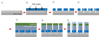
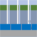
도 2는 일반적인 CIGS 단일형(monolithic) 모듈의 제조 완료된 단면 구조와 스크라이빙 영역을 나타낸 도면이다.
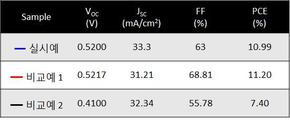
도 3은 본 발명의 실시예 (ITO와 Mo를 동시 이용) 와 기존의 비교예 1 (Mo 이용), 2 (ITO 이용) 의 기판별 효율 비교를 나타내기 위한 싱글 셀의 대한 효율 그래프(3a) 와 표(3b) 이다.
도 4는 본 발명의 실시예 (ITO와 Mo를 동시 이용) 와 기존의 비교예 1(Mo 이용), 2 (ITO 이용) 모듈의 제조 완료된 투과도 비교를 나타낸 사진이다.
Claims (8)
- (A) 투명성 절연 기판 위에 투명성 하부 전극층을 형성하는 단계,
(B) 상기 투명성 하부 전극층이 형성되어 있는 전체 영역인 셀 영역 중 일부인 투광 영역을 제외한 나머지 영역인 비투광 영역에 고전도성 비투명 하부 전극층을 형성시켜 복합 하부 전극층을 수득하는 단계,
(C) 상기 비투광 영역 중에서 그 일부 영역인 단락 영역에 대해서만 그 수직 하방향으로 존재하는 비투명성 하부 전극층 및 투명성 하부 전극층을 제거하고, 그 나머지 영역인 비단락 영역은 그대로 둠으로써, 서로 단락된 복수 개의 복합 하부 전극층을 수득하는 단계,
(D) 상기 (C) 단계를 거친 후 그 상부에 광흡수층, 버퍼층, 윈도우층을 형성시키는 단계,
(E) 상기 비투광성 영역 중 일부 영역인 도전성 영역의 수직 상하방향에 존재하는 상기 광흡수층, 상기 버퍼층, 상기 윈도우층을 제거하는 단계,
(F) 상기 (E) 단계를 거친 후 그 상부에 상부 전극층을 형성하는 단계,
(G) 상기 투광성 영역에 대해서 그 수직 상하방향에 존재하는 상기 광흡수층, 상기 버퍼층, 상기 윈도우층, 및 상기 상부 전극층을 제거하는 단계를 포함하는 태양전지 제조방법. - 제1항에 있어서, 상기 (B) 단계는 상기 투광 영역에 대해 마스킹한 후 상기 고전도성 비투명 하부 전극층을 형성하고 상기 마스킹을 제거함으로써 수행되는 것을 특징으로 하는 태양전지 제조방법.
- 제1항에 있어서, 상기 고전도성 비투명 전극층은 E-빔 증발법 또는 스퍼터링법에 의해 형성되는 것을 특징으로 하는 태양전지 제조방법.
- 제1항에 있어서, 상기 투과성 전극층은 ITO, FTO, AZO, graphene, 중에서 선택된 1종 이상이고,
상기 고전도성 비투명 전극층은 Mo, W, Cr, Ta, Nb, V, Ti, Mn 중에서 선택된 1종 이상인 것을 특징으로 하는 태양전지 제조방법. - 제1항에 있어서, 상기 (C) 단계는 레이저 스크라이빙법에 의해 수행되는 것을 특징으로 하는 태양전지 제조방법.
- 제1항에 있어서, 상기 (E) 단계는 메커니컬 스크라이빙법에 의해 수행되는 것을 특징으로 하는 태양전지 제조방법.
- 제1항에 있어서, 상기 (G) 단계는 메커니컬 스크라이빙법에 의해 수행되는 것을 특징으로 하는 태양전지 제조방법.
- 제1항 내지 제8항 중 어느 한 항에 따라 제조된 태양전지.
Priority Applications (1)
| Application Number | Priority Date | Filing Date | Title |
|---|---|---|---|
| KR1020180097398A KR20180098492A (ko) | 2018-08-21 | 2018-08-21 | 태양전지 및 그 제조방법 |
Applications Claiming Priority (1)
| Application Number | Priority Date | Filing Date | Title |
|---|---|---|---|
| KR1020180097398A KR20180098492A (ko) | 2018-08-21 | 2018-08-21 | 태양전지 및 그 제조방법 |
Related Parent Applications (1)
| Application Number | Title | Priority Date | Filing Date |
|---|---|---|---|
| KR1020170176981A Division KR20180055753A (ko) | 2017-12-21 | 2017-12-21 | 태양전지 및 그 제조방법 |
Related Child Applications (1)
| Application Number | Title | Priority Date | Filing Date |
|---|---|---|---|
| KR1020190041967A Division KR102174537B1 (ko) | 2019-04-10 | 2019-04-10 | 태양전지 및 그 제조방법 |
Publications (1)
| Publication Number | Publication Date |
|---|---|
| KR20180098492A true KR20180098492A (ko) | 2018-09-04 |
Family
ID=63598225
Family Applications (1)
| Application Number | Title | Priority Date | Filing Date |
|---|---|---|---|
| KR1020180097398A Ceased KR20180098492A (ko) | 2018-08-21 | 2018-08-21 | 태양전지 및 그 제조방법 |
Country Status (1)
| Country | Link |
|---|---|
| KR (1) | KR20180098492A (ko) |
Cited By (3)
| Publication number | Priority date | Publication date | Assignee | Title |
|---|---|---|---|---|
| KR20210052147A (ko) * | 2019-10-31 | 2021-05-10 | 한국과학기술연구원 | 씨스루형 박막 태양전지의 제조방법 |
| KR20220075838A (ko) * | 2020-11-30 | 2022-06-08 | 한국과학기술연구원 | 씨스루형 박막 태양전지 모듈 및 그의 제조방법 |
| US11495708B2 (en) | 2019-10-31 | 2022-11-08 | Korea Institute Of Science And Technology | Method of fabricating see-through thin film solar cell |
Citations (2)
| Publication number | Priority date | Publication date | Assignee | Title |
|---|---|---|---|---|
| US20080178925A1 (en) | 2006-12-29 | 2008-07-31 | Industrial Technology Research Institute | Thin film solar cell module of see-through type and method for fabricating the same |
| KR20150056833A (ko) | 2012-10-19 | 2015-05-27 | 가부시키가이샤 고베 세이코쇼 | 다관절 로봇의 위빙 제어 장치 |
-
2018
- 2018-08-21 KR KR1020180097398A patent/KR20180098492A/ko not_active Ceased
Patent Citations (2)
| Publication number | Priority date | Publication date | Assignee | Title |
|---|---|---|---|---|
| US20080178925A1 (en) | 2006-12-29 | 2008-07-31 | Industrial Technology Research Institute | Thin film solar cell module of see-through type and method for fabricating the same |
| KR20150056833A (ko) | 2012-10-19 | 2015-05-27 | 가부시키가이샤 고베 세이코쇼 | 다관절 로봇의 위빙 제어 장치 |
Non-Patent Citations (3)
| Title |
|---|
| 1. 논문게제 DOI: 10.1007/s11814-015-0200-1 |
| 2. 논문게제 DOI: 10.1002/pip.589 |
| 3. 논문게제 DOI:10.1016/j.apsusc.2011.08.016 |
Cited By (3)
| Publication number | Priority date | Publication date | Assignee | Title |
|---|---|---|---|---|
| KR20210052147A (ko) * | 2019-10-31 | 2021-05-10 | 한국과학기술연구원 | 씨스루형 박막 태양전지의 제조방법 |
| US11495708B2 (en) | 2019-10-31 | 2022-11-08 | Korea Institute Of Science And Technology | Method of fabricating see-through thin film solar cell |
| KR20220075838A (ko) * | 2020-11-30 | 2022-06-08 | 한국과학기술연구원 | 씨스루형 박막 태양전지 모듈 및 그의 제조방법 |
Similar Documents
| Publication | Publication Date | Title |
|---|---|---|
| CN102668120A (zh) | 太阳能电池设备及其制造方法 | |
| CN109888034A (zh) | 一种钙钛矿/背接触晶硅叠层太阳能电池 | |
| CN102856425A (zh) | 柔性硅基薄膜太阳电池集成组件的制备方法 | |
| CN101789458A (zh) | 变带隙双面透明电极薄膜太阳能电池 | |
| KR20180098492A (ko) | 태양전지 및 그 제조방법 | |
| KR102174537B1 (ko) | 태양전지 및 그 제조방법 | |
| CN104425651B (zh) | 一种低温制备正面无栅极的异质结太阳电池的工艺 | |
| KR101166456B1 (ko) | 태양전지 및 그 제조방법 | |
| CN104810420A (zh) | 透光型晶硅太阳电池组件 | |
| CN102237442B (zh) | 应用激光扫边机制作薄膜太阳能电池id的方法 | |
| KR101218503B1 (ko) | 얇은 알루미늄 박막을 이용한 태양전지 모듈 제조방법 | |
| CN101719520A (zh) | 透明导电极薄膜太阳能电池 | |
| CN101807612B (zh) | 薄膜太阳能电池及其制造方法 | |
| KR20180055753A (ko) | 태양전지 및 그 제조방법 | |
| CN202259339U (zh) | 一种具有高透光和正反双面发电功能的薄膜太阳能电池 | |
| CN102856421A (zh) | 一种新型三结薄膜太阳能电池及其生产方法 | |
| CN102544134A (zh) | 薄膜太阳能电池堆叠制造方法及其薄膜太阳能电池 | |
| CN103594552B (zh) | 一种光伏电池的制造方法 | |
| CN208062062U (zh) | 一种薄膜太阳能电池 | |
| CN102376825A (zh) | 一种制备薄膜太阳能透光组件的方法 | |
| JP2010027662A (ja) | 発電体及び発電体の製造方法 | |
| CN105489760A (zh) | 钙钛矿太阳电池透明导电衬底、制备方法及太阳电池 | |
| CN205231119U (zh) | 钙钛矿太阳电池透明导电衬底及其钙钛矿太阳电池 | |
| CN113782622A (zh) | 一种薄膜太阳能电池板及其制造方法 | |
| CN104269447B (zh) | 一种多晶硅太阳能电池板 |
Legal Events
| Date | Code | Title | Description |
|---|---|---|---|
| A107 | Divisional application of patent | ||
| A201 | Request for examination | ||
| PA0107 | Divisional application |
Comment text: Divisional Application of Patent Patent event date: 20180821 Patent event code: PA01071R01D Filing date: 20171221 Application number text: 1020170176981 |
|
| PA0201 | Request for examination | ||
| PG1501 | Laying open of application | ||
| E902 | Notification of reason for refusal | ||
| PE0902 | Notice of grounds for rejection |
Comment text: Notification of reason for refusal Patent event date: 20180910 Patent event code: PE09021S01D |
|
| A107 | Divisional application of patent | ||
| PA0107 | Divisional application |
Comment text: Divisional Application of Patent Patent event date: 20190410 Patent event code: PA01071R01D Filing date: 20171221 Application number text: 1020170176981 |
|
| E601 | Decision to refuse application | ||
| PE0601 | Decision on rejection of patent |
Patent event date: 20190418 Comment text: Decision to Refuse Application Patent event code: PE06012S01D Patent event date: 20180910 Comment text: Notification of reason for refusal Patent event code: PE06011S01I |